CN116247050A - Current Distribution Pin Structure and Forming Method - Google Patents
Current Distribution Pin Structure and Forming MethodDownload PDFInfo
- Publication number
- CN116247050A CN116247050ACN202210113341.4ACN202210113341ACN116247050ACN 116247050 ACN116247050 ACN 116247050ACN 202210113341 ACN202210113341 ACN 202210113341ACN 116247050 ACN116247050 ACN 116247050A
- Authority
- CN
- China
- Prior art keywords
- conductive structure
- conductive
- gate structures
- active region
- layer
- Prior art date
- Legal status (The legal status is an assumption and is not a legal conclusion. Google has not performed a legal analysis and makes no representation as to the accuracy of the status listed.)
- Pending
Links
Images


Classifications
- G—PHYSICS
- G06—COMPUTING OR CALCULATING; COUNTING
- G06F—ELECTRIC DIGITAL DATA PROCESSING
- G06F30/00—Computer-aided design [CAD]
- G06F30/30—Circuit design
- G06F30/39—Circuit design at the physical level
- G06F30/392—Floor-planning or layout, e.g. partitioning or placement
- G—PHYSICS
- G06—COMPUTING OR CALCULATING; COUNTING
- G06F—ELECTRIC DIGITAL DATA PROCESSING
- G06F30/00—Computer-aided design [CAD]
- G06F30/30—Circuit design
- G06F30/39—Circuit design at the physical level
- G06F30/394—Routing
- G—PHYSICS
- G06—COMPUTING OR CALCULATING; COUNTING
- G06F—ELECTRIC DIGITAL DATA PROCESSING
- G06F30/00—Computer-aided design [CAD]
- G06F30/30—Circuit design
- G06F30/39—Circuit design at the physical level
- G06F30/398—Design verification or optimisation, e.g. using design rule check [DRC], layout versus schematics [LVS] or finite element methods [FEM]
- H—ELECTRICITY
- H01—ELECTRIC ELEMENTS
- H01L—SEMICONDUCTOR DEVICES NOT COVERED BY CLASS H10
- H01L21/00—Processes or apparatus adapted for the manufacture or treatment of semiconductor or solid state devices or of parts thereof
- H01L21/70—Manufacture or treatment of devices consisting of a plurality of solid state components formed in or on a common substrate or of parts thereof; Manufacture of integrated circuit devices or of parts thereof
- H01L21/71—Manufacture of specific parts of devices defined in group H01L21/70
- H01L21/768—Applying interconnections to be used for carrying current between separate components within a device comprising conductors and dielectrics
- H—ELECTRICITY
- H01—ELECTRIC ELEMENTS
- H01L—SEMICONDUCTOR DEVICES NOT COVERED BY CLASS H10
- H01L23/00—Details of semiconductor or other solid state devices
- H01L23/52—Arrangements for conducting electric current within the device in operation from one component to another, i.e. interconnections, e.g. wires, lead frames
- H01L23/522—Arrangements for conducting electric current within the device in operation from one component to another, i.e. interconnections, e.g. wires, lead frames including external interconnections consisting of a multilayer structure of conductive and insulating layers inseparably formed on the semiconductor body
- H01L23/5222—Capacitive arrangements or effects of, or between wiring layers
- H—ELECTRICITY
- H01—ELECTRIC ELEMENTS
- H01L—SEMICONDUCTOR DEVICES NOT COVERED BY CLASS H10
- H01L23/00—Details of semiconductor or other solid state devices
- H01L23/52—Arrangements for conducting electric current within the device in operation from one component to another, i.e. interconnections, e.g. wires, lead frames
- H01L23/522—Arrangements for conducting electric current within the device in operation from one component to another, i.e. interconnections, e.g. wires, lead frames including external interconnections consisting of a multilayer structure of conductive and insulating layers inseparably formed on the semiconductor body
- H01L23/5226—Via connections in a multilevel interconnection structure
- H—ELECTRICITY
- H01—ELECTRIC ELEMENTS
- H01L—SEMICONDUCTOR DEVICES NOT COVERED BY CLASS H10
- H01L23/00—Details of semiconductor or other solid state devices
- H01L23/52—Arrangements for conducting electric current within the device in operation from one component to another, i.e. interconnections, e.g. wires, lead frames
- H01L23/522—Arrangements for conducting electric current within the device in operation from one component to another, i.e. interconnections, e.g. wires, lead frames including external interconnections consisting of a multilayer structure of conductive and insulating layers inseparably formed on the semiconductor body
- H01L23/528—Layout of the interconnection structure
- H—ELECTRICITY
- H10—SEMICONDUCTOR DEVICES; ELECTRIC SOLID-STATE DEVICES NOT OTHERWISE PROVIDED FOR
- H10D—INORGANIC ELECTRIC SEMICONDUCTOR DEVICES
- H10D84/00—Integrated devices formed in or on semiconductor substrates that comprise only semiconducting layers, e.g. on Si wafers or on GaAs-on-Si wafers
- H10D84/90—Masterslice integrated circuits
- H10D84/998—Input and output buffer/driver structures
- H—ELECTRICITY
- H10—SEMICONDUCTOR DEVICES; ELECTRIC SOLID-STATE DEVICES NOT OTHERWISE PROVIDED FOR
- H10D—INORGANIC ELECTRIC SEMICONDUCTOR DEVICES
- H10D89/00—Aspects of integrated devices not covered by groups H10D84/00 - H10D88/00
- H10D89/10—Integrated device layouts
- H—ELECTRICITY
- H10—SEMICONDUCTOR DEVICES; ELECTRIC SOLID-STATE DEVICES NOT OTHERWISE PROVIDED FOR
- H10D—INORGANIC ELECTRIC SEMICONDUCTOR DEVICES
- H10D84/00—Integrated devices formed in or on semiconductor substrates that comprise only semiconducting layers, e.g. on Si wafers or on GaAs-on-Si wafers
- H10D84/90—Masterslice integrated circuits
- H10D84/903—Masterslice integrated circuits comprising field effect technology
- H10D84/907—CMOS gate arrays
- H10D84/968—Macro-architecture
- H10D84/974—Layout specifications, i.e. inner core regions
- H10D84/975—Wiring regions or routing
Landscapes
- Engineering & Computer Science (AREA)
- Physics & Mathematics (AREA)
- Computer Hardware Design (AREA)
- General Physics & Mathematics (AREA)
- Theoretical Computer Science (AREA)
- Condensed Matter Physics & Semiconductors (AREA)
- Microelectronics & Electronic Packaging (AREA)
- Power Engineering (AREA)
- Geometry (AREA)
- Evolutionary Computation (AREA)
- General Engineering & Computer Science (AREA)
- Architecture (AREA)
- Manufacturing & Machinery (AREA)
- Computer Networks & Wireless Communication (AREA)
- Semiconductor Integrated Circuits (AREA)
- Metal-Oxide And Bipolar Metal-Oxide Semiconductor Integrated Circuits (AREA)
Abstract
Translated fromChinese
Description
Translated fromChinese技术领域Technical Field
本公开涉及电流分配引脚结构及其形成方法。The present disclosure relates to a current distribution pin structure and a method for forming the same.
背景技术Background Art
在金属中,电迁移(EM)是由导体中的阳离子(即,金属离子的正离子)的运动而引起的材料转移,该导体中的阳离子的运动是由于导电电子(即,运动中的电子)和阳离子之间的动量转移而引起的。导体材料的转移有可能在导体中产生断裂,从而形成开路,并且由此阻止电流流动。还有可能将导体材料转移到相邻导体并且造成电短路。在使用高直流(DC)密度的应用(例如,微电子和相关结构)中观察到EM。随着电子产品(例如,集成电路(IC))的结构尺寸减小,EM的实际意义增大。In metals, electromigration (EM) is the transfer of material caused by the movement of cations (i.e., positive ions of metal ions) in a conductor due to momentum transfer between conductive electrons (i.e., electrons in motion) and cations. The transfer of conductive material has the potential to create breaks in the conductor, thereby forming an open circuit and thereby preventing the flow of current. It is also possible to transfer conductive material to an adjacent conductor and cause an electrical short. EM is observed in applications using high direct current (DC) densities, such as microelectronics and related structures. As the size of electronic products, such as integrated circuits (ICs), decreases, the practical significance of EM increases.
随着小型化程度的提高,在超大规模集成(VLSI)和极大规模集成(ULSI)电路中,随着电流密度的增加(例如,随着导体尺寸减小,电流密度增加),由于EM而引起的故障增加。具体地,随着集成电路(IC)变得越来越小,导线宽度以及导线横截面面积随着时间的推移而继续减小。虽然电流会随着电源电压的降低和栅极电容的不断缩小而减少,但是电流减少会受到频率增加的限制。在电容电路中,随着频率增加,电流和电流密度也随之增加。此外,在没有可比较的电流减少的情况下,横截面面积减少得越多,IC的电流密度增加得越大,并且因此EM的风险就越大。As miniaturization increases, failures due to EM increase as current density increases (e.g., as conductor size decreases, current density increases) in very large scale integrated (VLSI) and ultra large scale integrated (ULSI) circuits. Specifically, as integrated circuits (ICs) become smaller, conductor widths and conductor cross-sectional areas continue to decrease over time. While current decreases with decreasing supply voltage and shrinking gate capacitance, the current reduction is limited by increasing frequency. In capacitive circuits, as frequency increases, current and current density also increase. Furthermore, the greater the reduction in cross-sectional area, the greater the increase in current density of the IC, and therefore the greater the risk of EM, without a comparable reduction in current.
发明内容Summary of the invention
根据本公开的一个实施例,提供了一种集成电路(IC)中的电流分配结构,所述结构包括:衬底;第一有源区域和第二有源区域,所述第一有源区域和所述第二有源区域在所述衬底上在第一方向上相应地延伸,所述第二有源区域与所述第一有源区域在基本垂直于所述第一方向的第二方向上分离;第一组栅极结构和第二组栅极结构,所述第一组栅极结构和所述第二组栅极结构在所述第二方向上延伸并且与所述第一有源区域和所述第二有源区域相应地交叠;第一导电结构,在第一金属化层中,所述第一导电结构在所述第一方向上延伸、至少部分地与所述第一有源区域交叠、并且电耦合到所述第一组栅极结构;第二导电结构,在所述第一金属化层中,所述第二导电结构在所述第一方向上延伸、至少部分地与所述第二有源区域交叠、并且电耦合到所述第二组栅极结构;以及第三导电结构,在第二金属化层中,所述第三导电结构在所述第二方向上延伸、至少部分地与所述第一导电结构和所述第二导电结构交叠、并且电耦合到所述第一导电结构和所述第二导电结构。According to an embodiment of the present disclosure, a current distribution structure in an integrated circuit (IC) is provided, the structure comprising: a substrate; a first active region and a second active region, the first active region and the second active region respectively extending in a first direction on the substrate, the second active region being separated from the first active region in a second direction substantially perpendicular to the first direction; a first group of gate structures and a second group of gate structures, the first group of gate structures and the second group of gate structures extending in the second direction and correspondingly overlapping with the first active region and the second active region; a first conductive structure, in a first metallization layer, the first conductive structure extending in the first direction, at least partially overlapping with the first active region, and electrically coupled to the first group of gate structures; a second conductive structure, in the first metallization layer, the second conductive structure extending in the first direction, at least partially overlapping with the second active region, and electrically coupled to the second group of gate structures; and a third conductive structure, in a second metallization layer, the third conductive structure extending in the second direction, at least partially overlapping with the first conductive structure and the second conductive structure, and electrically coupled to the first conductive structure and the second conductive structure.
根据本公开的另一实施例,提供了一种制造集成电路(IC)的方法,所述IC与存储在非暂态计算机可读介质上的布局图相对应,所述方法包括生成所述布局图,所述生成所述布局图包括:生成在衬底形状上在第一方向上相应地延伸的第一有源区域形状和第二有源区域形状,所述第二有源区域形状与所述第一有源区域形状在基本垂直于所述第一方向的第二方向上分离;生成在所述第二方向上延伸并且与所述第一有源区域形状和所述第二有源区域形状相应地交叠的第一组栅极结构形状和第二组栅极结构形状;生成包括第一导电形状和第二导电形状的第一金属化层,所述第一导电形状在所述第一方向上延伸、至少部分地与所述第一有源区域形状交叠,并且所述第二导电形状在所述第一方向上延伸、至少部分地与所述第二有源区域形状交叠;生成包括第三导电形状的第二金属化层,所述第三导电形状在所述第二方向上延伸、至少部分地与所述第一导电形状和所述第二导电形状交叠;以及生成包括第四导电形状的第三金属化层,所述第四导电形状在所述第一方向上延伸、并且至少部分地与所述第三导电形状交叠。According to another embodiment of the present disclosure, a method for manufacturing an integrated circuit (IC) is provided, the IC corresponding to a layout diagram stored on a non-transitory computer-readable medium, the method comprising generating the layout diagram, wherein generating the layout diagram comprises: generating a first active area shape and a second active area shape extending correspondingly in a first direction on a substrate shape, the second active area shape being separated from the first active area shape in a second direction substantially perpendicular to the first direction; generating a first group of gate structure shapes and a second group of gate structure shapes extending in the second direction and correspondingly overlapping with the first active area shape and the second active area shape; generating a first metallization layer comprising a first conductive shape and a second conductive shape, the first conductive shape extending in the first direction and at least partially overlapping with the first active area shape, and the second conductive shape extending in the first direction and at least partially overlapping with the second active area shape; generating a second metallization layer comprising a third conductive shape, the third conductive shape extending in the second direction and at least partially overlapping with the first conductive shape and the second conductive shape; and generating a third metallization layer comprising a fourth conductive shape, the fourth conductive shape extending in the first direction and at least partially overlapping with the third conductive shape.
根据本公开的又一实施例,提供了一种制造集成电路(IC)的方法,所述方法包括:制造在衬底上在第一方向上相应地延伸的第一有源区域和第二有源区域,所述第二有源区域与所述第一有源区域在基本垂直于所述第一方向的第二方向上分离;制造在所述第二方向上延伸并且与所述第一有源区域和所述第二有源区域相应地交叠的第一组栅极结构和第二组栅极结构;形成包括第一导电结构和第二导电结构的第一金属化层,所述第一导电结构在所述第一方向上延伸、至少部分地与所述第一有源区域交叠,并且所述第二导电结构在所述第一方向上延伸、至少部分地与所述第二有源区域交叠;以及形成包括第三导电结构的第二金属化层,所述第三导电结构在所述第二方向上延伸、至少部分地与所述第一导电结构和所述第二导电结构交叠。According to another embodiment of the present disclosure, a method for manufacturing an integrated circuit (IC) is provided, the method comprising: manufacturing a first active region and a second active region extending respectively in a first direction on a substrate, the second active region being separated from the first active region in a second direction substantially perpendicular to the first direction; manufacturing a first group of gate structures and a second group of gate structures extending in the second direction and correspondingly overlapping with the first active region and the second active region; forming a first metallization layer comprising a first conductive structure and a second conductive structure, the first conductive structure extending in the first direction and at least partially overlapping with the first active region, and the second conductive structure extending in the first direction and at least partially overlapping with the second active region; and forming a second metallization layer comprising a third conductive structure extending in the second direction and at least partially overlapping with the first conductive structure and the second conductive structure.
附图说明BRIEF DESCRIPTION OF THE DRAWINGS
在结合附图阅读时,可以从下面的具体实施方式中最佳地理解本公开的各方面。应当注意,根据行业的标准做法,各种特征不是按比例绘制的。事实上,为了讨论的清楚起见,各种特征的尺寸可能被任意增大或减小。When read in conjunction with the accompanying drawings, various aspects of the present disclosure can be best understood from the following detailed description. It should be noted that, in accordance with standard practice in the industry, various features are not drawn to scale. In fact, the size of various features may be arbitrarily increased or reduced for clarity of discussion.
图1是根据一些实施例的包括具有多接入点输入的区域的集成电路(IC)的框图。1 is a block diagram of an integrated circuit (IC) including a region with a multi-access point input, according to some embodiments.
图2A是根据一些实施例的电流分布输入引脚结构的局部布局图。FIG. 2A is a partial layout diagram of a current distribution input pin structure according to some embodiments.
图2B是根据一些实施例的半导体器件的布局图。FIG. 2B is a layout diagram of a semiconductor device according to some embodiments.
图2C是根据一些实施例的半导体器件的偏移横截面图。FIG. 2C is an offset cross-sectional view of a semiconductor device in accordance with some embodiments.
图2D是根据一些实施例的半导体器件的布局图。FIG. 2D is a layout diagram of a semiconductor device according to some embodiments.
图2E是根据一些实施例的半导体器件的布局图。FIG. 2E is a layout diagram of a semiconductor device according to some embodiments.
图2F是根据一些实施例的半导体器件的布局图。FIG. 2F is a layout diagram of a semiconductor device according to some embodiments.
图2G是根据一些实施例的半导体器件的布局图。FIG. 2G is a layout diagram of a semiconductor device according to some embodiments.
图3A是根据一些实施例的半导体器件的布局图。FIG. 3A is a layout diagram of a semiconductor device according to some embodiments.
图3B是根据一些实施例的半导体器件的偏移横截面图。FIG. 3B is an offset cross-sectional view of a semiconductor device in accordance with some embodiments.
图3C是根据一些实施例的半导体器件的布局图。FIG. 3C is a layout diagram of a semiconductor device according to some embodiments.
图3D是根据一些实施例的半导体器件的布局图。FIG. 3D is a layout diagram of a semiconductor device according to some embodiments.
图3E是根据一些实施例的半导体器件的布局图。FIG. 3E is a layout diagram of a semiconductor device according to some embodiments.
图3F是根据一些实施例的半导体器件的布局图。FIG. 3F is a layout diagram of a semiconductor device according to some embodiments.
图3G是根据一些实施例的半导体器件的布局图。FIG. 3G is a layout diagram of a semiconductor device according to some embodiments.
图4A是根据一些实施例的电流分布输入引脚结构的局部布局图。FIG. 4A is a partial layout diagram of a current distribution input pin structure according to some embodiments.
图4B是根据一些实施例的半导体器件的布局图。FIG. 4B is a layout diagram of a semiconductor device according to some embodiments.
图4C是根据一些实施例的半导体器件的偏移横截面图。FIG. 4C is an offset cross-sectional view of a semiconductor device in accordance with some embodiments.
图5是根据一些实施例的制造半导体器件的方法的流程图。FIG. 5 is a flowchart of a method of manufacturing a semiconductor device according to some embodiments.
图6A是根据一些实施例的制造半导体器件的方法的流程图。FIG. 6A is a flowchart of a method of manufacturing a semiconductor device according to some embodiments.
图6B是根据一些实施例的生成用于半导体器件的布局图的方法的流程图。FIG. 6B is a flow chart of a method of generating a layout map for a semiconductor device according to some embodiments.
图7是根据一些实施例的电子设计自动化(EDA)系统的框图。7 is a block diagram of an electronic design automation (EDA) system according to some embodiments.
图8是根据一些实施例的IC制造系统以及与其相关联的IC制造流程的框图。8 is a block diagram of an IC manufacturing system and an IC manufacturing flow associated therewith, according to some embodiments.
具体实施方式DETAILED DESCRIPTION
不受理论的束缚,本文提供了基础物理学的解释。下面的公开内容提供了用于实现所提供的主题的不同特征的许多不同实施例或示例。下文描述了组件、值、操作、材料、布置等的具体示例以简化本公开。当然,这些仅仅是示例而不意图是限制性的。预期其他组件、值、操作、材料、布置等。例如,在下面的说明中,在第二特征上方或之上形成第一特征可以包括以直接接触的方式形成第一特征和第二特征的实施例,并且还可以包括可以在第一特征和第二特征之间形成附加特征,使得第一特征和第二特征可以不直接接触的实施例。此外,本公开可以在各种示例中重复参考标号和/或字母。该重复是为了简单和清楚的目的,并且本身并不表示所讨论的各个实施例和/或配置之间的关系。Without being bound by theory, an explanation of the underlying physics is provided herein. The following disclosure provides many different embodiments or examples for realizing the different features of the subject matter provided. Specific examples of components, values, operations, materials, arrangements, etc. are described below to simplify the disclosure. Of course, these are merely examples and are not intended to be restrictive. Other components, values, operations, materials, arrangements, etc. are contemplated. For example, in the following description, forming a first feature above or on a second feature may include an embodiment in which the first feature and the second feature are formed in direct contact, and may also include an embodiment in which additional features may be formed between the first feature and the second feature so that the first feature and the second feature may not be in direct contact. In addition, the disclosure may repeat reference numerals and/or letters in various examples. This repetition is for the purpose of simplicity and clarity, and does not itself represent the relationship between the various embodiments and/or configurations discussed.
此外,本文中可能使用了空间相关术语(例如,“下方”、“之下”、“低于”、“以上”、“上部”等),以易于描述图中所示的一个要素或特征相对于另外(一个或多个)要素或(一个或多个)特征的关系。这些空间相关术语意在涵盖器件在使用或工作中除了图中所示朝向之外的不同朝向。装置可能以其他方式定向(旋转90度或处于其他朝向),并且本文中所用的空间相关描述符同样可能被相应地解释。Additionally, spatially relative terms (e.g., "below," "beneath," "below," "above," "upper," etc.) may be used herein to facilitate describing the relationship of one element or feature illustrated in the figures relative to another element(s) or feature(s). These spatially relative terms are intended to encompass different orientations of the device in use or operation in addition to the orientation depicted in the figures. The device may be otherwise oriented (rotated 90 degrees or at other orientations) and the spatially relative descriptors used herein may likewise be interpreted accordingly.
在一些实施例中,半导体器件具有金属化层,该金属化层包括具有更多数量的接入点(即,过孔)的输入引脚(与另一种方法相比)。一些实施例的增加数量的接入点的好处在于,每个接入点输入电流的均方根(RMS)降低至少20%(与其他方法相比)。在一些实施例中,每个接入点输入电流的RMS降低超过约20%。在一些实施例中,每个接入点输入电流的RMS降低多达约50%。在一些实施例中,AC电流的RMS是将在电阻负载中产生相同功率耗散的DC电流的值。在一些实施例中,在第一金属化层中实现每个接入点电流的RMS的降低。In some embodiments, a semiconductor device has a metallization layer that includes input pins with a greater number of access points (i.e., vias) than another approach. A benefit of the increased number of access points in some embodiments is that the root mean square (RMS) of the input current per access point is reduced by at least 20% (compared to other approaches). In some embodiments, the RMS of the input current per access point is reduced by more than about 20%. In some embodiments, the RMS of the input current per access point is reduced by as much as about 50%. In some embodiments, the RMS of the AC current is the value of the DC current that would produce the same power dissipation in a resistive load. In some embodiments, the reduction in the RMS of the current per access point is achieved in the first metallization layer.
在一些实施例中,具有第一金属化层(第M_1层)的半导体器件包括在半导体器件的第一侧上的第一导电结构以及在半导体器件的第二侧上的第二导电结构。在一些实施例中,第一导电结构和第二导电结构中的每一者都电耦合到第二金属化层(第M_2层)。在一些实施例中,第M_2层形成作为输入引脚的第三导电结构。在一些实施例中,第三导电结构在第一位置(例如,接入点)处电耦合到第一导电结构,并且在第二位置(例如,接入点)处电耦合到第二导电结构。在一些实施例中,将第M_1层分离为第一导电结构和第二导电结构降低了第一接入点和第二接入点中的每一者处的电流密度。在一些实施例中,针对第一导电结构、第二导电结构和第三导电结构的将第M_1层与第M_2层电耦合的多个接入点防止了在输入引脚(第M_2层)上的一个接入点处的累积电流密度。在一些实施例中,输入引脚上的接入点处的电流密度的降低防止或显著减少了EM退化的风险。在一些实施例中,第M_2层包括两个或更多个接入点,该两个或更多个接入点分配电流,并且防止或显著减少EM。在一些实施例中,半导体器件高度不随着对第M_1层和第M_2层的修改而改变。在一些实施例中,这种结构改变是在对任何标准半导体器件进行最小修改的情况下执行的。In some embodiments, a semiconductor device having a first metallization layer (layer M_1) includes a first conductive structure on a first side of the semiconductor device and a second conductive structure on a second side of the semiconductor device. In some embodiments, each of the first conductive structure and the second conductive structure is electrically coupled to the second metallization layer (layer M_2). In some embodiments, the layer M_2 forms a third conductive structure as an input pin. In some embodiments, the third conductive structure is electrically coupled to the first conductive structure at a first position (e.g., an access point) and is electrically coupled to the second conductive structure at a second position (e.g., an access point). In some embodiments, separating the layer M_1 into the first conductive structure and the second conductive structure reduces the current density at each of the first access point and the second access point. In some embodiments, multiple access points for electrically coupling the layer M_1 to the layer M_2 for the first conductive structure, the second conductive structure, and the third conductive structure prevent the cumulative current density at one access point on the input pin (layer M_2). In some embodiments, the reduction in current density at the access point on the input pin prevents or significantly reduces the risk of EM degradation. In some embodiments, the M_2 layer includes two or more access points that distribute current and prevent or significantly reduce EM. In some embodiments, the semiconductor device height does not change with modifications to the M_1 layer and the M_2 layer. In some embodiments, this structural change is performed with minimal modification to any standard semiconductor device.
图1是根据一些实施例的包括具有多接入点输入的区域102的集成电路(IC)100的框图。1 is a block diagram of an integrated circuit (IC) 100 including a
在一些实施例中,IC 100包括区域102,该区域102包括导电分段,该导电分段具有更多数量的接入点以及通过接入点的相应更小电流以防止EM退化,即,每个接入点具有减少的电流。在一些实施例中,IC 100是单片IC(也称为芯片或微芯片),该单片IC是在半导体材料(例如,硅)的一个平坦片(例如,芯片或衬底)上的一组电子电路。在一些实施例中,IC100包括在衬底上的大量金属氧化物半导体(MOS)晶体管。In some embodiments,
在一些实施例中,IC 100包括逻辑电路和/或存储器电路等。在一些实施例中,IC100包括通过光刻而构建到单片半导体衬底上的电子网络中的小型化电子组件。In some embodiments,
在一些实施例中,IC 100包括微处理器、现场可编程门阵列(FPGA)、存储器(例如,RAM、ROM和闪存)和专用集成电路(ASIC)。在一些实施例中,IC 100包括运算放大器、线性调节器、锁相环、振荡器和有源滤波器。In some embodiments,
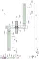
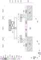
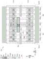
图2A和图2B是相对应的并且是根据一些实施例的布局图。图2B是根据一些实施例的具有图2A的电流分配输入引脚结构204的半导体器件的布局图。图2A是图2B的简化版本。图2A包括未在图2B中示出的电容器226A-226F;图2A中的电容器226A-226F表示寄生电容,并且被包括在图2A中以用于为RMS电流的数学表示(参见下文)提供上下文。图2C是根据一些实施例的图2B的半导体器件的偏移横截面图;相应地,图2B中的相应横截面线IIC是偏移或阶梯状的,并且包括分段246(1)、246(2)、246(3)、246(4)和246(5),它们代表图2C的相应相同编号部分。Figures 2A and 2B correspond and are layout diagrams according to some embodiments. Figure 2B is a layout diagram of a semiconductor device having the current distribution
图2A-图2B的布局图表示半导体器件中的结构。在图2A-图2B中,半导体器件中的结构由布局图中的形状(也称为图案)表示。为了讨论的简单起见,图2A-图2B(以及本文包括的其他附图)的布局图中的元素将被称为结构而不是形状本身。例如,图2B中的形状228表示图2C中的有源区域228(也称为氧化物尺寸(OD)区域);在下面的讨论中,元素228被称为有源区域228。The layout diagrams of FIGS. 2A-2B represent structures in a semiconductor device. In FIGS. 2A-2B , the structures in the semiconductor device are represented by shapes (also referred to as patterns) in the layout diagrams. For simplicity of discussion, the elements in the layout diagrams of FIGS. 2A-2B (and other figures included herein) will be referred to as structures rather than shapes themselves. For example,
在图2A-图2B的布局图中,在IC 100中在区域102中使用电流分配输入引脚结构204,该电流分配输入引脚结构204包括导电分段,该导电分段具有更多数量的接入点以及通过接入点的相应更小电流以防止EM退化。In the layout diagrams of FIGS. 2A-2B , a current distribution
在一些实施例中,IC(例如,IC 100)包括衬底(图2B-图2C中的206),该衬底包括第一有源区域和第二有源区域(图2B和图2C中的228、232),该第一有源区域和第二有源区域在衬底206上在第一方向上(沿着图2A-图2B中的X轴)相应地延伸。第二有源区域(图2B和图2C中的232)与第一有源区域(图2B和图2C中的228)在基本垂直于第一方向的第二方向上(沿着图2A-图2B中Y轴)分离。在一些实施例中,第一方向和第二方向是除了X轴和Y轴的相应方向之外的方向。IC 100还包括栅极结构244(1)、244(2)、244(3)、244(4)、244(5)、244(6)、244(7)和244(8)。栅极结构被组织成包括栅极结构244(1)-244(4)的第一组以及包括栅极结构244(5)-244(8)的第二组。相对于Y轴,切割图案(CP)与相应栅极结构的近似中线交叠。在图2B中,切割图案与栅极结构244(1)和244(8)中的每一者交叠,这表明栅极结构244(1)和244(8)中的每一者的相应上部部分与相应下部部分电隔离。在一些实施例中,第一组栅极结构和第二组栅极结构(图2B中的234、236)在第二方向上延伸并且与第一有源区域和第二有源区域(图2B中的228、232)相应地交叠。在一些实施例中,第一金属化层(第M_1层)(参见图2C中的208)中的第一导电结构210在第一方向上延伸、至少部分地与第一有源区域(图2B和图2C中的228)交叠、并且电耦合到第一组栅极结构(图2B中的234)。第一导电结构210与栅极结构244(2)-244(4)交叠。在一些实施例中,第M_1层208中的第二导电结构212在第一方向上延伸、至少部分地与第二有源区域(图2B和图2C中的232)交叠、并且电耦合到第二组栅极结构(图2B中的236)。第二导电结构212与栅极结构244(5)-244(7)交叠。在一些实施例中,第二金属化层(第M_2层)(参见图2C中的216)中的第三导电结构214在第二方向上延伸。第三导电结构214通过过孔218和219电耦合到第一导电结构210和第二导电结构212,并且至少部分地与第一导电结构210和第二导电结构212交叠。过孔218和219在第一互连层(第V_1层)中(参见图2C中的217)。在一些实施例中,根据制造这种半导体器件的相应工艺节点的编号惯例,第M_1层208是金属化层0(M0)或金属化层1(M1),并且相应地,互连的第V_1层是VIA0或VIA1。在一些实施例中,M0是晶体管层(参见图2C中的205)之上的第一金属化层。在图2C中,晶体管层205包括衬底206、有源区域228和232、栅极结构244(4)和244(5)、和到栅极的过孔(VG)结构240和241。In some embodiments, an IC (e.g., IC 100) includes a substrate (206 in FIGS. 2B-2C) including a first active region and a second active region (228, 232 in FIGS. 2B and 2C) extending in a first direction (along the X axis in FIGS. 2A-2B) on the
在一些实施例中,衬底206是用于制造IC的半导体薄片,例如晶体硅(c-Si)。在一些实施例中,衬底206用作构建在衬底206中和衬底206上的微电子器件的基底。在一些实施例中,衬底经历许多微制造工艺,例如掺杂、离子注入、蚀刻、各种材料的薄膜沉积、和光刻图案化。In some embodiments,
在一些实施例中,供体杂质原子(例如,在硅的情况下,是硼或磷)可以以精确的量被添加到本征衬底材料中以掺杂晶体,从而将其改变为n型或p型的非本征半导体。在一些实施例中,这些n型或p型半导体区域被称为有源区域,例如有源区域(图2B和图2C中的228、232)。In some embodiments, donor impurity atoms (e.g., boron or phosphorus in the case of silicon) can be added to the intrinsic substrate material in precise amounts to dope the crystal, thereby changing it to an n-type or p-type extrinsic semiconductor. In some embodiments, these n-type or p-type semiconductor regions are referred to as active regions, such as active regions (228, 232 in FIGS. 2B and 2C).
在一些实施例中,第一组栅极结构和第二组栅极结构(图2B中的234、236)由包括金属(例如,铝)或多晶硅的材料制成。在一些实施例中,在MOS晶体管中,向第一组栅极结构和第二组栅极结构(图2B中的234、236)中的任何一个栅极施加电压,进而改变有源区域(图2B和图2C中的228、232)之间的导电性。In some embodiments, the first and second gate structures (234, 236 in FIG. 2B) are made of a material including a metal (e.g., aluminum) or polysilicon. In some embodiments, in a MOS transistor, a voltage is applied to any gate of the first and second gate structures (234, 236 in FIG. 2B), thereby changing the conductivity between the active regions (228, 232 in FIG. 2B and FIG. 2C).
在一些实施例中,第M_1层208和第三金属化层(第M_3层)(参见图2C中的239)是沿着X方向延伸的导电层,并且第M_2层216是在Y方向上延伸的导电层。在一些实施例中,第M_1层208在每个到栅极的过孔(VG)结构(图2B中的VG结构240和241)之上延伸,并且第M_2层216在每个过孔218和219之上,并且由此被配置为提供VG结构240和241以及过孔218和219之间的低电阻路径。导电分段是被配置为通过包括一种或多种导电材料(例如,金属(例如,铜、铝、钨或钛)、多晶硅、或能够提供低电阻路径的其他材料)来提供低电阻路径的体积件(volume)。在一些实施例中,导电分段包括一种或多种导电材料,被配置为一个或多个阻挡层。In some embodiments, the
在一些实施例中,通过第一导电结构210的电流由箭头220A和220B表示。在一些实施例中,电流220A和220B是通过第一组(图2B中的234)中的一个或多个栅极结构传导到第一导电结构210的电流。在一些实施例中,电流220A、220B是来自第一组栅极结构(图2B中的234)所位于的电流分配输入引脚结构204的左侧222的电流。In some embodiments, currents through the first
在一些实施例中,通过第二导电结构212的电流由箭头220C和220D表示。在一些实施例中,电流220C和220D是通过第二组(图2B中的236)中的一个或多个栅极结构传导到第二导电结构212的电流。在一些实施例中,电流220C、220D是来自第二组栅极结构(图2B中的236)所位于的电流分配输入引脚结构204的右侧224的电流。In some embodiments, the currents through the second
在一些实施例中,电流220A、220B通过过孔218传导到第三导电结构214,该过孔218将第一导电结构210电耦合到第三导电结构214。在一些实施例中,电流220C、220D通过过孔219传导到第三导电结构214,该过孔219将第二导电结构212电耦合到第三导电结构214。在一些实施例中,电流220A、220B组合为电流220E,并且电流220C、220D组合为电流220F,该电流220E和电流220F传导通过过孔221,该过孔221将导电结构214与第M_3层239中的导电结构238电耦合,其中过孔221在第二互连层(第V_2层)(图2C中的237)中。In some embodiments,
相比于使用十字形引脚(cross-type pin)的其他方法(其中通过第M_1层中的单个导电结构的电流通过单个接入点(即,单个过孔)电耦合到第M_2层中的相应单个导电结构),在图2A-图2C的实施例中,来自第一导电结构210的电流220A和220B通过过孔218电耦合到导电结构214,并且来自第二导电结构212的电流220C和220D通过过孔219电耦合到导电结构214。因此,一些实施例的优点是进入导电结构214的总电流被分配通过两个过孔,即过孔218和219。在一些实施例中,与其他方法相比,RMS电流在过孔218和219处有效地减少了一半。在一些实施例中,随着第M_1层中的导电结构的数量和相应的过孔的数量增加超过两个,每个过孔的RMS电流相应地减小。在一些实施例中,每个过孔的电流为约1/N,其中N是表示过孔的数量的正整数。例如,在第三导电结构214处结合两个接入点(例如,过孔218和219),将通过每个过孔218和219的RMS电流有效地减少了一半。三个接入点(即,三个过孔)(例如,图4A、图4B和图4C所示)将通过每个接入点的RMS电流有效地降低了2/3,即,每个过孔传导的电流是根据其他方法的十字形引脚中的单个过孔的电流的1/3。Compared to other methods using cross-type pins, in which the current through a single conductive structure in the M_1 layer is electrically coupled to the corresponding single conductive structure in the M_2 layer through a single access point (i.e., a single via), in the embodiments of FIGS. 2A-2C,
在图2A中,电流(由箭头220A、220B、220C和220D表示)被示出为在第一导电结构210和第二导电结构212中。在其他方法(例如,十字形方法)中,电流220A、220B、220C和220D在单个接入点处组合。因此,在其他方法中,导电结构中的组合电流在一个接入点处累积。在一些实施例中,半导体器件具有导电结构214,其包括具有更多数量的接入点218、219(即,过孔)的输入引脚(与其他方法相比)。一些实施例的增加数量的接入点的好处在于,每个接入点输入电流的均方根(RMS)降低了至少20%(与其他方法相比)。在一些实施例中,AC电流的RMS是将在电阻负载中产生相同功率耗散的DC电流的值。In FIG. 2A , current (represented by
IRMS=0.707·IACMax=IDC=有效电流 等式(1)IRMS = 0.707·IACMax = IDC = effective current equation (1)
在图2C中,对于第M_2层208中的给定导电结构,在用于输入引脚的多个接入点(第V_1层217中的过孔218和219)之间分配电流,通过降低每个接入点(第V_1层217中的每个过孔218和219)的RMS电流并且因此降低电流密度,来防止或阻止EM退化。电流密度是每单位时间流过单位面积的选定横截面的电荷数量。电流密度矢量
在其他方法中,尤其是在汽车工业中,EM是一个问题,因为温度梯度较高并且温度随时间的变化较小。描述通过互连分段(例如,接入点,例如,过孔)的原子浓度的控制等式是质量平衡连续性等式。质量原子通量出现在流体力学的一些等式中,具体地,连续性等式是流体的质量守恒的表述。在流体力学中,质量只能从一处流向另一处。In other methods, especially in the automotive industry, EM is a problem because of high temperature gradients and small changes in temperature over time. The governing equation describing the concentration of atoms through an interconnect segment (e.g., an access point, such as a via) is the mass balance continuity equation. Mass atomic flux appears in some equations in fluid mechanics, specifically the continuity equation is a statement of the conservation of mass for a fluid. In fluid mechanics, mass can only flow from one place to another.

其中,
下面的等式3示出了对总原子通量的主要贡献。原子通量是原子的扩散。这种原子的扩散以及导电电子之间的动量转移会产生EM退化。因此,控制或降低原子通量有助于防止或控制EM退化。

总电流密度是电流


在一些实施例中,在温度较高并且随时间变化不大或变化很小的情况下,用于减轻否则增加的EM风险的技术是降低电流。因此,如图2A所示,通过降低电流RMS(例如,拆分电流220A、220B和220C、220D),降低了EM退化的可能性。In some embodiments, where the temperature is high and does not vary much or very little over time, a technique for mitigating otherwise increased EM risk is to reduce the current. Thus, as shown in FIG. 2A , by reducing the current RMS (e.g., splitting the
任何点(例如,接入点,例如图2B中的过孔218或219)处的电流在特定时间点处用欧姆定律来表示。The current at any point (eg, an access point, such as via 218 or 219 in FIG. 2B ) is expressed by Ohm's law at a particular point in time.

用文字来表述等式(4),时间(t)处的电流是时间(t)处的电压除以接入点的电阻。结合接入点的总阻抗产生:Expressing equation (4) in words, the current at time (t) is the voltage at time (t) divided by the resistance of the access point. Combining this with the total impedance of the access point yields:

其中,
求解电流,RMS为:Solving for the current, RMS is:

根据等式(6),随着电容增加(例如,由图2A中的寄生电容器226A-226F象征性地表示),RMS电流增加,并且随着温度增加,RMS电流增加。因此,当情况合适时,例如在温度升高的环境中(例如,在靠近在195°F至220°F或91℃至105℃之间运行的车辆发动机的应用中),更可能发生EM退化。According to equation (6), as capacitance increases (e.g., symbolically represented by
在其他方法中,第M_1层和第M_2层中的导电分段的布置通俗地称为十字形引脚。对于十字形引脚,第M_2层中的导电分段相对于M_1层中的导电分段垂直地延伸、跨越在第M_1层中的导电分段之上、并且电耦合至第M_1层中的导电分段,第M_1层中的导电分段水平地跨越半导体器件延伸。第M_1层和第M_2层中的导电分段组合在一起,类似于十字或字母X。在该其他方法中,所有电流都通过一个接入点(即,一个过孔),其将第M_1层中的导电分段电耦合到第M_2层中的导电分段。In other methods, the arrangement of the conductive segments in the M_1 layer and the M_2 layer is colloquially referred to as a cross pin. For the cross pin, the conductive segments in the M_2 layer extend vertically relative to the conductive segments in the M_1 layer, cross over the conductive segments in the M_1 layer, and are electrically coupled to the conductive segments in the M_1 layer, and the conductive segments in the M_1 layer extend horizontally across the semiconductor device. The conductive segments in the M_1 layer and the M_2 layer are combined together, similar to a cross or the letter X. In this other method, all currents pass through one access point (i.e., one via), which electrically couples the conductive segments in the M_1 layer to the conductive segments in the M_2 layer.
在图2A中,VG结构(图2B和图2C中的240、241)的电容由寄生电容器226A-226F象征性地表示,其中在图2A中示出了寄生电容器226A、226C、226D和226F,但是没有示出寄生电容器226B和226E(为了说明的简单起见)。此外,第M_1层上的所有接入点的电容是相加的,因为它们是并联的。因此,参考上面的等式(6),电容在半导体器件中被最大化,因为第M_1层中的给定导电结构上的每个到栅极的过孔(VG)结构的电容是累积的。在其他方法中,第M_3层中的导电结构被添加以形成额外的输入引脚,该额外的输入引脚通过额外的过孔与第M_2层中的另一导电结构耦合。然而,该其他方法限制了在电路制造期间的自动布局布线(APR)性能(例如,在电路设计中布线和放置其他元件的能力)。In FIG. 2A , the capacitance of the VG structure (240, 241 in FIG. 2B and FIG. 2C ) is symbolically represented by
在其他方法中,柱状件(pillar)(第M_3层中的导电结构)与多个输入引脚互连以减轻输入引脚处的过大电流。然而,根据其他方法的添加额外的输入引脚和/或柱状件会限制电路的布线资源,增加APR流程(因为电路的灵活性被限制),并且在添加金属层的情况下寄生电容仍然是问题。In other approaches, pillars (conductive structures in the M_3 layer) are interconnected with multiple input pins to mitigate excessive current at the input pins. However, adding additional input pins and/or pillars according to other approaches limits the wiring resources of the circuit, increases the APR process (because the flexibility of the circuit is limited), and parasitic capacitance is still a problem when adding metal layers.
在图2A中,VG结构(图2B和图2C中的240、241)的电容由电容器226A-226F象征性地表示,其中在图2A中示出了电容器226A、226C、226D和226F,但是没有示出电容器226B和226E(为了说明的简单起见)。参考等式(6),在一些实施例中,随着电容降低,RMS电流成比例地降低。在图2B中,通过第M_1层208中的相应导电结构来馈送电流的VG结构的数量与第V_1层中的过孔(例如,过孔218和219)的比率减少了一半(与根据其他方法的十字形引脚的比率相比)。相应地,在图2B中,由于VG结构的数量与第V_1层中的给定过孔的比率降低而产生的电容减小,有助于降低通过第V_1层中的给定过孔的RMS电流,并且因此有助于防止EM。在一些实施例中,随着电容增加,RMS电流也增加。In FIG. 2A , the capacitance of the VG structures ( 240 , 241 in FIGS. 2B and 2C ) is symbolically represented by
对于图2B,半导体器件230包括:衬底206;第一有源区域228和第二有源区域232,在衬底206上;第一组栅极结构234和第二组栅极结构236,与第一有源区域228和第二有源区域232相应地部分交叠;第一导电结构210,与第一有源区域228交叠;第二导电结构212,与第二有源区域232部分交叠;以及第三导电结构214,与第一导电结构210和第二导电结构212部分交叠。2B , the
在图2B中,第一组栅极结构234通过VG结构240电耦合到第一导电结构210。在一些实施例中,VG结构240电耦合到组234中的一个或多个栅极结构244(1)-244(4)的上部部分242。在一些实施例中,第二组栅极结构236通过VG结构241电耦合到第二导电结构212,VG结构241电耦合到组236中的一个或多个栅极结构244(5)-244(8)的上部部分242。2B , a first group of
再次,图2C是根据一些实施例的图2B的半导体器件的偏移横截面视图。图2C表示的横截面线在图2B中被示出为横截面线IIC。Again, Figure 2C is an offset cross-sectional view of the semiconductor device of Figure 2B according to some embodiments. The cross-sectional line represented by Figure 2C is shown as cross-sectional line IIC in Figure 2B.
在图2C中,再次图2C是偏移横截面视图,第一导电结构210通过过孔218电耦合到第三导电结构214。在一些实施例中,第二导电结构212通过过孔219电耦合到第三导电结构214。在一些实施例中,第M_2层216中的第三导电结构214电耦合到过孔221,该过孔221将导电结构214与第M_3层239中的导电结构238电耦合,其中过孔221在第二互连层(第V_2层)(图2C中的237)中。In FIG2C , again FIG2C is an offset cross-sectional view, the first
图2D、图2E、图2F和图2G是根据一些实施例的具有电流分配输入引脚结构204的半导体器件230的变体的相应布局图。2D , 2E , 2F , and 2G are respective layout diagrams of variations of a
在一些实施例中,如图2D所示,第M_1层208中的第一导电结构210和第二导电结构212通过设置在有源区域228和232之间的额外的第M_1层电耦合到一个或多个栅极结构。在一些实施例中,如图2D-图2G所示,第一导电结构210和第二导电结构212被缩短(相对于图2B中的X轴)并且在三个栅极结构(例如,图2D、图2F和图2G)或更少的栅极结构(例如,图2E)之上延伸。在每个图2D、图2F和图2G中,导电结构210与栅极结构244(3)-244(5)交叠,并且导电结构212与栅极结构244(5)-244(7)交叠。在图2E中,导电结构210与栅极结构244(4)-244(5)交叠,并且导电结构212与栅极结构244(5)-244(6)交叠。在图2D-图2G中,第一组栅极结构234和/或第二组栅极结构236通过位于有源区域228和232之间的、在第M_1层208中的额外的导电结构电耦合。在图2D-图2G中,这些额外的导电结构不耦合到第M_2层216内的导电结构214;而是替代地,这些额外的导电结构通过共同连接的栅极结构耦合到第M_1层208内的第一导电结构210和/或第二导电结构212,例如在图2E-图2G中。在一些实施例中,第M_1层208内的额外的导电结构电耦合到第M_2层216内的额外的导电结构(而不是共同电耦合的栅极),例如在图2D中。即,第M_2层216中的额外的导电结构用于电耦合第M_1层208内的额外的导电结构,该第M_1层208内的额外的导电结构还电耦合到第M_1层208内的第一导电结构210和第二导电结构212。In some embodiments, as shown in FIG2D , the first
图3A是根据一些实施例的半导体器件330的布局图。FIG. 3A is a layout diagram of a
在一些实施例中,图3A与图2B的不同之处在于,半导体330通过下列方式将RMS电流降低了约50%:沿着水平方向使用切割图案348拆分栅极结构344(1)、344(2)、344(3)、344(4)、344(5)、344(6)、344(7)、344(8)和344(9),来控制栅极结构344(2)-344(8)的哪些部分由接入点318服务并且栅极结构344(2)-344(8)的哪些部分由接入点319服务。然而,在图2B中,每个栅极结构244(2)-244(4)的整体由接入点218服务,并且每个栅极结构244(5)-244(7)的整体由接入点219服务;相比之下,在图3A中,栅极结构344(2)-344(8)的上部部分由接入点318服务,并且栅极结构344(2)-344(8)的下部部分由接入点319服务。In some embodiments, FIG. 3A differs from FIG. 2B in that
图3A的布局图类似于图2B的布局图。图3A遵循与图2B类似的编号惯例。虽然对应,但是一些组件也不同。为了帮助识别对应但仍有差异的组件,图3A使用3系列编号,而图2B使用2系列编号。为简洁起见,讨论将更多地集中在图2B和图3A之间的差异上,而不是相似之处。The layout diagram of FIG. 3A is similar to the layout diagram of FIG. 2B. FIG. 3A follows a similar numbering convention as FIG. 2B. Although corresponding, some components are also different. To help identify components that correspond but are still different, FIG. 3A uses a 3-series numbering while FIG. 2B uses a 2-series numbering. For the sake of brevity, the discussion will focus more on the differences between FIG. 2B and FIG. 3A rather than the similarities.
图3A的布局图表示半导体器件中的结构。在图3A中,半导体器件中的结构由布局图中的形状(也称为图案)表示。为了讨论的简单起见,图3A(以及本文包括的其他附图)的布局图中的元素将被称为结构而不是形状本身。例如,图3A中的形状328表示图3B中的有源区域328(也称为氧化物尺寸(OD)区域);在下面的讨论中,元素328被称为有源区域328。The layout diagram of FIG. 3A represents a structure in a semiconductor device. In FIG. 3A , the structure in the semiconductor device is represented by a shape (also referred to as a pattern) in the layout diagram. For simplicity of discussion, the elements in the layout diagram of FIG. 3A (and other figures included herein) will be referred to as structures rather than shapes themselves. For example,
在一些实施例中,半导体器件330是包括在IC 100中的一个或多个半导体器件之一。在一些实施例中,半导体器件330包括在IC 100中在区域102中使用的电流分配输入引脚结构304,并且该电流分配输入引脚结构304包括导电分段,该导电分段具有更多数量的接入点以及通过接入点的相应更小电流以防止EM退化。In some embodiments,
在一些实施例中,IC(例如,IC 100)包括:衬底306;第一有源区域328和第二有源区域332,在衬底306上在第一方向上(沿着X轴)相应地延伸,第二有源区域332与第一有源区域328在基本垂直于第一方向的第二方向上(沿着Y轴)分离。第一组栅极结构334和第二组栅极结构336在第二方向上延伸,其中第一组栅极结构334与第一有源区域328相应地交叠,并且第二组栅极结构336与第二有源区域332相应地交叠。第M_1层(图3B中的308)内的第一导电结构310在第一方向上延伸,与第一有源区域328交叠,并且与包括每个栅极结构344(2)、344(3)、344(4)、344(5)、344(6)、344(7)和344(8)的第一组栅极结构334交叠并与其电耦合。第M_1层308内的第二导电结构312在第一方向上延伸,与第二有源区域332交叠,并且与包括栅极结构344(2)、344(3)、344(4)、344(5)、344(6)、344(7)和344(8)的第二组栅极结构336交叠并与其电耦合。第M_2层316内的在第二方向上延伸的第三导电结构314通过第一互连层(第V_1层)(参见图3B中的317)内的过孔结构318和319电耦合到第一导电结构310和第二导电结构312。在一些实施例中,第M_2层316中的第三导电结构314电耦合到过孔321,该过孔321将导电结构314与第M_3层339中的导电结构338电耦合,其中过孔321在第二互连层(第V_2层)(图3B中的337)中。过孔318和319在第一互连层(第V_1层)(参见图3B中的317)中。在图3B中,晶体管层305包括衬底306、有源区域328和332、栅极结构344(4)、344(5)和344(6)、和到栅极的过孔(VG)结构340和341。In some embodiments, an IC (e.g., IC 100) includes a
图3B是根据一些实施例的半导体器件330的偏移横截面视图。FIG. 3B is an offset cross-sectional view of a
图3B表示的横截面线在图3A中被示出为偏移横截面线IIIB。图3B中的线IIIB的部分346(1)、346(2)、346(3)、346(4)和346(5)对应于图3A中的线IIIB的相同编号分段。The cross-sectional line represented in Figure 3B is shown as offset cross-sectional line IIIB in Figure 3A. Portions 346(1), 346(2), 346(3), 346(4), and 346(5) of line IIIB in Figure 3B correspond to the same numbered segments of line IIIB in Figure 3A.
在一些实施例中,M0是晶体管层305之上的第一金属化层。晶体管层305包括衬底306、有源区域328和332、栅极结构334和336、以及到栅极的过孔(VG)结构340和341。在一些实施例中,根据制造这种半导体器件的相应工艺节点的编号惯例,第M_1层308是金属化层0(M0)或金属化层1(M1),并且相应地,第V_1层是VIA0或VIA1。在一些实施例中,M0是晶体管层305之上的第一金属化层。过孔318和319在第一互连层(第V_1层)317中。在一些实施例中,第M_2层316中的第三导电结构314电耦合到过孔321,该过孔321将导电结构314与第M_3层339中的导电结构338电耦合,其中过孔321在第二互连层337中。In some embodiments, M0 is the first metallization layer above
在一些实施例中,第一组栅极结构334通过过孔结构340电耦合到第M_1层308内的第一导电结构310。在一些实施例中,第二组栅极结构336通过过孔结构341电耦合到第M_1层308内的第二导电结构312,该过孔结构341电耦合到第二组栅极结构336。在一些实施例中,栅极结构344(1)-344(8)被切割图案348交叠,该切割图案348表示将完整的原有栅极结构电分离为多个栅极结构。在图3A中,切割图案348与栅极结构344(1)-344(8)中的每一者交叠,这表明栅极结构344(1)-344(8)中的每一者的相应上部部分与相应下部部分电隔离。在一些实施例中,切割图案348表示将相应栅极结构344(1)-344(8)的上部部分和下部部分分隔开的间隙。在一些实施例中,由切割图案348表示的间隙填充有电介质材料,该电介质材料表示相应上部部分和相应下部部分之间的电不连续性。In some embodiments, the first group of
在一些实施例中,第M_1层308内的第一导电结构310通过第一互连层(第V_1层)317内的过孔结构318电耦合到第M_2层316内的第三导电结构314。在一些实施例中,第M_1层308内的第二导电结构312通过第V_1层317内的过孔结构319电耦合到第M_2层316内的第三导电结构314,该过孔结构319与第二导电结构312电耦合。In some embodiments, the first
与通过将栅极结构垂直地分离为第一组栅极结构234和第二组栅极结构236来降低半导体器件电流的半导体器件230进行比较,半导体器件330通过将栅极结构水平地分离为第一组栅极结构334和第二组栅极结构336来降低半导体器件电流。在一些实施例中,半导体器件230中的接入点218和219处的RMS电流的减少与接入点318和319处的RMS电流减少大致相同;减少了一半。Compared to
与其他方法的十字形引脚(其中通过第M_1层中的单个导电结构的电流在一个接入点处累积)进行比较,在一些实施例中,提供给第一导电结构310的电流与提供给第二导电结构312的电流通过切割图案348分隔开。在一些实施例中,RMS电流在过孔318和319处相应有效地减少了一半。Compared to the cross pins of other methods (in which the current through a single conductive structure in the M_1th layer is accumulated at one access point), in some embodiments, the current provided to the first
在图3C、图3D、图3E、图3F和图3G中,描绘了根据一些实施例的具有电流分配输入引脚结构304的半导体器件330。In FIGS. 3C , 3D, 3E, 3F, and 3G, a
在图3C中,切割图案348的一部分延伸跨越左侧322,而不具有切割图案的相应部分延伸跨越右侧324。更具体地,在图3C中,切割图案348包括与栅极结构344(1)-344(4)和344(9)共同交叠的两个部分。在一些实施例中,切割图案328的一部分延伸跨越右侧324,而不具有切割图案的相应部分延伸跨越左侧322。在图3D和图3F中,切割图案348在左侧322上的栅极结构的第一子集(即,少于全部)并且在右侧324上的栅极结构的第二子集(即,少于全部)之上延伸。更具体地,在图3D中,切割图案348包括与栅极结构344(1)-344(3)和344(7)-344(9)共同交叠的两个部分。在图3E和图3G中的每一者中,切割图案348包括与栅极结构344(1)和344(9)共同交叠的两个部分。在一些实施例中,基于在接入点318和319处要实现的减小的电流量,来选择由切割图案348产生的栅极结构中的间隙的数量。在图3E和图3G中,切割图案348与有源栅极结构不交叠,即栅极结构344(2)-344(8)。在一些实施例中,栅极结构在电耦合到第一导电结构310或第二导电结构312之间交替,例如,如图3G所示。在一些实施例中,相对于图3A上的X轴,第一导电结构310或第二导电结构312的长度缩短并且耦合到最靠近第三导电结构314的一个或多个栅极结构,例如,图3G中的第二导电结构312。In FIG3C , a portion of the
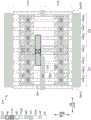
图4A和图4B是相对应的布局图。图4A是根据一些实施例的电流分配输入引脚结构404的局部布局图。图4A是图4B的简化版本。图4C是根据一些实施例的半导体器件430的偏移横截面视图。图4A的布局图类似于图2A的布局图。图4B和图4C的布局图类似于图2A、图2C和图3B的布局图。图4B遵循与图2B和图3A类似的编号惯例。虽然对应,但是一些组件也不同。为了帮助识别对应但仍有差异的组件,图4A使用4系列编号,而图2B使用2系列编号并且图3A使用3系列编号。为简洁起见,讨论将更多地集中在图2B和图4A之间的差异上,而不是相似之处。4A and 4B are corresponding layout diagrams. FIG. 4A is a partial layout diagram of a current distribution
在一些实施例中,在IC 100中在区域102中使用电流分配输入引脚结构404,该电流分配输入引脚结构404包括导电分段,该导电分段具有更多数量的接入点以及通过接入点的相应更小电流以防止EM退化。在一些实施例中,电流分配输入引脚结构404类似于电流分配输入引脚结构204,因为它们各自都用于降低位于输入引脚上的接入点处的电流、RMS电流和电流密度。In some embodiments, a current distribution
在一些实施例中,半导体器件430(图4B)包括衬底406(图4B和图4C),该衬底406包括第一有源区域和第二有源区域(图4B和图4C中的428、432),该第一有源区域和第二有源区域在衬底406上在第一方向上(沿着X轴)相应地延伸。在一些实施例中,第二有源区域(图4B和图4C中的432)与第一有源区域(图4B和图4C中的428)在基本垂直于第一方向的第二方向上(沿着Y轴)分离。半导体器件430还包括栅极结构444(1)、444(2)、444(3)、444(4)、444(5)、444(6)、444(7)、448(8)和444(9)。栅极结构被组织成包括栅极结构444(1)-444(5)的上部部分的第一组、包括栅极结构444(1)-444(5)的下部部分的第二组、以及包括栅极结构444(6)-444(9)的第三组。第一组栅极结构、第二组栅极结构和第三组栅极结构(图4B中的434、435和436)在第二方向上延伸。在一些实施例中,第一组栅极结构和第三组栅极结构(图4B中的434、436)与第一有源区域(图4B中的428)相应地交叠。在一些实施例中,第二组栅极结构和第三组栅极结构(图4B中的435、436)与第二有源区域(图4B中的432)相应地交叠。在一些实施例中,第M_1层408(图4C)内的第一导电结构410在第一方向上延伸,至少部分地与第一有源区域(图4B和图4C中的428)交叠,并且电耦合到第一组栅极结构(图4B中的434)。在一些实施例中,第M_1层408(图4C)内的第二导电结构412在第一方向上延伸,至少部分地与第二有源区域(图4B和图4C中的432)交叠,并且电耦合到第二组栅极结构(图4B中的435)。在一些实施例中,第M_1层408(图4C)内的第三导电结构411在第一有源区域和第二有源区域(图4B和图4C中的428、432)之间在第一方向上延伸,并且电耦合到第三组栅极结构(图4B中的436)。相对于Y轴,第三导电结构411位于第一有源区域和第二有源区域之间,即,与第一有源区域和第二有源区域不交叠。在一些实施例中,第M_2层416(图4C)内的第四导电结构414在第二方向上延伸。第四导电结构414通过相应过孔418、415和419电耦合到第一导电结构410、第二导电结构412和第三导电结构411,并且至少部分地与第一导电结构410、第二导电结构412和第三导电结构411交叠。过孔418、415和419在第一互连层(第V_1层)(参见图4C中的417)中。在一些实施例中,根据制造这种半导体器件的相应工艺节点的编号惯例,第M_1层408是金属化层0(M0)或金属化层1(M1),并且相应地,第V_1层是VIA0或VIA1。在一些实施例中,M0是晶体管层(参见图4C的405)之上的第一金属化层。在图4C中,晶体管层405包括衬底406、有源区域428和432、栅极结构444(5)和444(6)、和到栅极的过孔(VG)结构440和441。In some embodiments, semiconductor device 430 (FIG. 4B) includes substrate 406 (FIG. 4B and FIG. 4C), which includes a first active region and a second active region (428, 432 in FIG. 4B and FIG. 4C), which extend in a first direction (along the X axis) on
在一些实施例中,通过第一导电结构410的电流由箭头420A和420B表示。在一些实施例中,电流420A和420B是通过第一组(图4B中的434)中的一个或多个栅极结构传导到第一导电结构410的电流。在一些实施例中,电流420A、420B是来自第一组栅极结构(图4B中的434)所位于的电流分配输入引脚结构404的左上侧422的电流。In some embodiments, currents through the first
在一些实施例中,通过第二导电结构412的电流由箭头420C和420D表示。在一些实施例中,电流420C和420D是通过第二组(图4B中的435)中的一个或多个栅极结构传导到第二导电结构412的电流。在一些实施例中,电流420C、420D是来自第二组栅极结构(图4B中的435)所位于的电流分配输入引脚结构404的左下侧423的电流。In some embodiments, the current through the second
在一些实施例中,通过第三导电结构411的电流由箭头420E和420F表示。在一些实施例中,电流420E和420F是通过第三组(图4B中的436)中的一个或多个栅极结构传导到第三导电结构411的电流。在一些实施例中,电流420E、420F是来自第三组栅极结构(图4B中的436)所位于的电流分配输入引脚结构404的右侧424的电流。In some embodiments, the current through the third
在一些实施例中,电流420A、420B通过过孔418传导到第四导电结构414,该过孔418将第一导电结构410电耦合到第四导电结构414。在一些实施例中,电流420C、420D通过过孔419传导到第四导电结构414,该过孔419将第二导电结构412电耦合到第四导电结构414。在一些实施例中,电流420E、420F通过过孔415传导到第四导电结构414,该过孔415将第三导电结构411电耦合到第四导电结构414。在一些实施例中,电流420A、420B、420C、420D、420E和420F组合并且传导通过过孔421,该过孔421将第四导电结构414与第M_3层(图4C中的439)内的导电结构(图4A-图4C中的438)电耦合。In some embodiments,
与根据其他方法的十字形引脚(其中通过第M_1层中的单个导电结构的电流在一个接入点处累积)进行比较,在一些实施例中,(1)提供给第一导电结构410的电流420A和420B、(2)提供给第二导电结构412的电流420C和420D、以及(3)提供给第三导电结构411的电流420E和420F中的每一者通过相应过孔418、419和415彼此分隔开。在图4A-图4C中,针对第四导电结构414结合三个接入点(例如,过孔418、415和419),在每个接入点处将RMS电流有效地降低了2/3(与根据其他方法的十字形引脚的单个接入点相比)。Compared to a cross pin according to other approaches (in which currents through a single conductive structure in the M_1-th layer are accumulated at one access point), in some embodiments, each of (1)
在一些实施例中,VG结构(图4B和图4C中的443、440、441)的电容由电容器426A、426B(图4A中未示出)、426C、426D、426E(图4A中未示出)、426F、426G、426H(图4A中未示出)和426I象征性表示。在一些实施例中,位于第一组(图4B中的434)中的一个或多个栅极结构与第一导电结构410之间的、位于第二组(图4B中的435)中的一个或多个栅极结构与第二导电结构412之间的、以及位于第三组(图4B中的436)中的一个或多个栅极结构与第三导电结构411之间的VG结构(图4B和图4C的443、440、441)处的电容还通过在第一导电结构410、第二导电结构412和第三导电结构411之间进行分隔而被减少。通过将第M_1层408分隔为第一导电结构410、第二导电结构412和第三导电结构411,第M_1层408的电容在(1)第三导电结构411与(2)第一导电结构410和第二导电结构412之间被有效地减半。在一些实施例中,第M_1层408的电容在第一导电结构410和第二导电结构412之间再次被减半,因为它们被切割图案448分隔开。参考上面的等式(6),在一些实施例中,随着电容降低,RMS电流直接降低。这与根据其他方法的十字形引脚形成对比,在该其他方法中第M_1层中的导电结构的电容不被分隔,这产生可能引起EM退化的RMS电流水平。在一些实施例中,随着电容增加,RMS电流也增加。In some embodiments, the capacitance of the VG structure (443, 440, 441 in FIGS. 4B and 4C) is symbolically represented by
图4B是根据一些实施例的具有电流分配输入引脚结构404的半导体器件430的布局图。FIG. 4B is a layout diagram of a
在一些实施例中,半导体器件430是在IC 100中使用的许多半导体器件之一。在一些实施例中,半导体器件430包括在IC 100中在区域102中使用的电流分配输入引脚结构404。该电流分配输入引脚结构404包括导电分段,该导电分段具有更多数量的接入点以及通过每个接入点的相应更小电流,这防止了EM退化。在一些实施例中,电流分配输入引脚结构404类似于电流分配输入引脚结构204,因为它们各自都用于降低位于输入引脚上的接入点处的电流、RMS电流和电流密度。In some embodiments,
在一些实施例中,半导体器件430包括:衬底406;第一有源区域428和第二有源区域432,在衬底406上;第一组栅极结构434、第二组栅极结构435和第三组栅极结构436;第一导电结构410,在第M_1层408中;第二导电结构412,在第M_1层408中;第三导电结构411,在第M_1层408中;以及第四导电结构414,在第M_2层416中。In some embodiments, the
图4C是根据一些实施例的具有电流分配引脚结构404的半导体器件430的偏移横截面视图。FIG. 4C is an offset cross-sectional view of a
图4C表示的横截面线在图4B中被示出为偏移横截面线IVC。图4C中的部分446(1)、446(2)、446(3)、446(4)、446(5)、446(6)、446(7)、446(8)和446(9)对应于图4B中的线IVC的相同编号分段。The cross-sectional line represented in Figure 4C is shown as offset cross-sectional line IVC in Figure 4B. Portions 446(1), 446(2), 446(3), 446(4), 446(5), 446(6), 446(7), 446(8), and 446(9) in Figure 4C correspond to the same numbered segments of line IVC in Figure 4B.
在一些实施例中,第一组栅极结构434通过VG结构443电耦合到第M_1层408内的第一导电结构410。在一些实施例中,VG结构443电耦合到组434中的一个或多个栅极结构。在一些实施例中,第二组栅极结构435通过VG结构440电耦合到第二导电结构412,该VG结构440电耦合到组435中的一个或多个栅极结构。在一些实施例中,第三组栅极结构436通过VG结构441电耦合到第三导电结构411,该VG结构441电耦合到组436中的一个或多个栅极结构。In some embodiments, the first group of
在一些实施例中,第一导电结构410通过过孔结构418电耦合到第四导电结构414。在一些实施例中,第二导电结构412通过过孔结构419电耦合到第四导电结构414。在一些实施例中,第三导电结构411通过过孔415电耦合到第四导电结构414。In some embodiments, the first
在一些实施例中,第M_2层416中的第四导电结构414电耦合到过孔421,该过孔421将导电结构414与第M_3层439中的导电结构438电耦合,其中过孔421位于第二互连层(第V_2层)437中。过孔418、415和419位于第一互连层(第V_1层)417中。In some embodiments, fourth
图5是根据一些实施例的制造半导体器件的方法的流程图。FIG. 5 is a flowchart of a method of manufacturing a semiconductor device according to some embodiments.
在一些实施例中,在图5中描绘的方法500之前、期间和/或之后执行附加操作,并且一些其他过程在本文中仅简要描述。根据方法500制造的半导体器件的示例包括根据相应图2B、图3A和图4B等的布局图的半导体器件。In some embodiments, additional operations are performed before, during, and/or after the
图5包括框502、504、506、508和510。在方法500的框502处,制造在衬底上在第一方向上延伸的第一有源区域和第二有源区域。此外,第二有源区域与第一有源区域在基本垂直于第一方向的第二方向上分隔开。作为非限制性示例,在如图2B、图3A和图4B所示的实施例中,有源区域228、232、328、332、428和432制造在衬底的顶部或内部。继续该示例,第一有源区域228、328和428在第一方向上(沿着X轴)延伸。第二有源区域232、332和432也在第一方向上延伸,但是与第一有源区域228、328和428垂直地在第二方向上(沿着Y轴)分隔开。从框502,流程进行到框504。Fig. 5 includes
在方法500的框504处,制造在第二方向上延伸并且与第一有源区域和第二有源区域交叠的第一组栅极结构和第二组栅极结构。作为非限制性示例,在如图2B、图3A和图4B所示的实施例中,第一组栅极结构234、334和434在第二方向上(沿着Y轴)延伸并且与第一有源区域228、328和428交叠。继续该示例,第二组栅极结构236、336和435在第二方向上延伸并且与第二有源区域232、332和432交叠。从框504,流程进行到框506。At
在方法500的框506处,形成第一金属化层,该第一金属化层包括在第一方向上延伸并与第一有源区域交叠的第一导电结构以及在第一方向上延伸并与第二有源区域交叠的第二导电结构。作为非限制性示例,在如图2B、图3A和图4B所示的实施例中,第一金属化层208、308和408包括在第一方向上(沿着X轴)延伸并与第一有源区域228、328和428交叠的第一导电结构210、310和410。继续该示例,第一金属化层208、308和408包括在第一方向上延伸并与第二有源区域232、332和432交叠的第二导电结构212、312和412。从框506,流程进行到框508。At
在方法500的框508处,形成包括第三导电结构的第二金属化层,并且该第三导电结构在第二方向上延伸、至少部分地与第一导电结构和第二导电结构交叠。作为非限制性示例,在如图2B、图3A和图4B所示的实施例中,第二金属化层216、316和416包括在第二方向上(沿着Y轴)延伸并且至少部分地与第一导电结构210、310和410以及第二导电结构212、312和412交叠的第三导电结构214、314和414。从框508,流程进行到框510。At
在方法500的框510处,在第一导电结构和第三导电结构之间形成第一过孔,并且在第二导电结构和第三导电结构之间形成第二过孔。作为非限制性示例,在如图2B、图3A和图4B所示的实施例中,第一过孔218、318和418电耦合在第一导电结构210、310和410与第三导电结构214、314和414之间。继续该示例,第二过孔219、319和419电耦合在第二导电结构212、312、和412与第三导电结构214、314和414之间。At
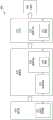
图6A是根据一些实施例的制造半导体器件的方法600的流程图。FIG. 6A is a flow chart of a
根据一些实施例,方法600是可例如使用EDA系统700(图7,在下面进行讨论)和集成电路(IC)制造系统800(图8,在下面进行讨论)来实现。能够根据方法600制造的半导体器件的示例包括图1的IC 100、对应于本文公开的各种布局图的半导体器件等等。According to some embodiments,
在图6中,方法600包括框602-604。在框602处,生成布局图,该布局图除了其他之外,包括本文公开的一个或多个布局图等等。根据一些实施例,块602可例如使用EDA系统700(图7,在下面进行讨论)来实现。In Figure 6,
更具体地,框602包括生成与在半导体图中要被表示的结构相对应的形状。例如,关于框602:在生成的布局图对应于单元区域202A的情况下,框602包括生成与单元区域202A中所示的结构相对应的形状;在生成的布局图对应于单元区域202E的情况下,框602包括生成与单元区域202E中所示的结构相对应的形状;在生成的布局图对应于单元区域202F的情况下,框602包括生成与单元区域202F中所示的结构相对应的形状;在生成的布局图对应于单元区域302A的情况下,框602包括生成与单元区域302A中所示的结构相对应的形状;在生成的布局图对应于单元区域302B的情况下,框602包括生成与单元区域302B中所示的结构相对应的形状;在生成的布局图对应于单元区域302C的情况下,框602包括生成与单元区域302C中所示的结构相对应的形状;等等。从框602,流程进行到框604。More specifically, block 602 includes generating shapes corresponding to structures to be represented in the semiconductor diagram. For example, with respect to block 602: where the generated layout diagram corresponds to cell region 202A, block 602 includes generating shapes corresponding to the structures shown in cell region 202A; where the generated layout diagram corresponds to cell region 202E, block 602 includes generating shapes corresponding to the structures shown in cell region 202E; where the generated layout diagram corresponds to cell region 202F, block 602 includes generating shapes corresponding to the structures shown in cell region 202F; where the generated layout diagram corresponds to cell region 302A, block 602 includes generating shapes corresponding to the structures shown in cell region 302A; where the generated layout diagram corresponds to cell region 302B, block 602 includes generating shapes corresponding to the structures shown in cell region 302B; where the generated layout diagram corresponds to cell region 302C, block 602 includes generating shapes corresponding to the structures shown in cell region 302C; and so on. From
在框604处,基于布局图,进行下列项中的至少一项:(A)进行一次或多次光刻曝光;或(B)制造一个或多个半导体掩模;或(C)制造半导体器件的层中的一个或多个组件。参见下面图8的讨论。At
图6B是根据一些实施例的生成布局图的方法的流程图。FIG. 6B is a flowchart of a method of generating a layout map according to some embodiments.
更具体地,图6B的流程图示出了根据一个或多个实施例的包括在图6A的框602中的附加框。框602包括框610-622。根据一些实施例,方法600是可例如使用EDA系统700(图7,在下面进行讨论)和集成电路(IC)制造系统800(图8,在下面进行讨论)来实现。能够根据方法600制造的半导体器件的示例包括图1的IC 100、对应于本文公开的各种布局图的半导体器件等等。More specifically, the flowchart of FIG. 6B illustrates additional blocks included in
在方法600的框610处,生成在衬底上在第一方向上延伸的第一有源区域和第二有源区域。此外,第二有源区域与第一有源区域在基本垂直于第一方向的第二方向上分隔开。作为非限制性示例,在如图2B、图3A和图4B所示的实施例中,有源区域228、232、328、332、428和432生成在衬底的顶部或内部。继续该示例,第一有源区域228、328和428在第一方向上(沿着X轴)延伸。第二有源区域232、332和432也在第一方向上延伸,但是与第一有源区域228、328和428垂直地在第二方向上(沿着Y轴)分隔开。从框610,流程进行到框612。At the
在方法600的框612处,生成在第二方向上延伸并且与第一有源区域和第二有源区域交叠的第一组栅极结构和第二组栅极结构。第一组栅极结构的非限制性示例包括相应图2B、图3A和图4B中的栅极结构组234、334和434,该栅极结构组234、334和434在第二方向上(沿着Y轴)延伸并且与相应第一有源区域228、328和428等交叠。第二组栅极结构的非限制性示例包括相应图2B、图3A和图4B中的组236、336和435,该组236、336和435在第二方向上延伸并且与相应第二有源区域232、332和432交叠。从框612,流程进行到框614。At
在方法600的框614处,生成第M_1层,该第M_1层包括在第一方向上延伸并与第一有源区域交叠的第一导电结构以及在第一方向上延伸并与第二有源区域交叠的第二导电结构。第M_1层的非限制性示例包括相应图2B、图3A和图4B中的第一金属化层的第M_1层208、308和408。第一导电结构的非限制性示例包括导电结构210、310和410,该导电结构210、310和410在第一方向上(沿着X轴)延伸并且与相应第一有源区域228、328和428等交叠。第二导电结构的非限制性示例包括相应图2B、图3A和图4B中的导电结构212、312和412,该导电结构212、312和412在第一方向上延伸并且与相应第二有源区域232、332和432交叠。从框614,流程进行到框620。At
在方法600的框620处,生成第M_2层,该第M_2层包括在第二方向上延伸并且至少部分地与第一导电结构和第二导电结构中的每一者交叠的第三导电结构。第M_2层的非限制性示例包括相应图2B、图3A和图4B中的第M_2层216、316和416。第三导电结构的非限制性示例包括导电结构214、314和414,该导电结构214、314和414在第二方向上(沿着Y轴)延伸并且至少部分地与相应第一导电结构210、310和410以及相应第二导电结构212、312和412交叠。从框620,流程前进到框622。At
在方法600的框622处,生成第M_3层,该第M_3层包括在第一方向上延伸并且至少部分地与第三导电结构交叠的第四导电结构。第M_3层的非限制性示例包括相应图2B、图3A和图4B中的第M_3层239、339或439。第四导电结构的非限制性示例包括导电结构238、338和438,该导电结构238、338和438在第一方向上(沿着X轴)延伸并且至少部分地与相应第三导电结构214、314、414等交叠。At
图7是根据一些实施例的电子设计自动化(EDA)系统700的框图。FIG. 7 is a block diagram of an electronic design automation (EDA)
在一些实施例中,EDA系统700包括自动布局布线(APR)系统。根据一个或多个实施例,本文描述的用于设计表示电线布线布置的布局图的方法例如根据一些实施例可使用EDA系统700来实施。In some embodiments,
在一些实施例中,EDA系统700是通用计算设备,包括硬件处理器702和非暂态计算机可读存储介质704。除其他之外,存储介质704被编码有(即,存储有)计算机程序代码706(即,一组可执行指令)。硬件处理器702执行指令706(至少部分地)表示实现根据一个或多个实施例的本文描述的方法(在下文中,所提及的过程和/或方法)的一部分或全部的EDA工具。In some embodiments, the
处理器702经由总线708电耦合至计算机可读存储介质704。处理器702还经由总线708电耦合至I/O接口710。网络接口712还经由总线708电耦合至处理器702。网络接口712连接到网络714,使得处理器702和计算机可读存储介质704能够经由网络714连接到外部元件。处理器702被配置为执行编码在计算机可读存储介质704中的计算机程序代码706,以使得系统700可用于执行所提到的过程和/或方法的一部分或全部。在一个或多个实施例中,处理器702是中央处理单元(CPU)、多处理器、分布式处理系统、专用集成电路(ASIC)、和/或合适的处理单元。The
在一个或多个实施例中,计算机可读存储介质704是电的、磁的、光的、电磁的、红外的、和/或半导体系统(或装置或设备)。例如,计算机可读存储介质704包括半导体或固态存储器、磁带、可移动计算机磁盘、随机存取存储器(RAM)、只读存储器(ROM)、刚性磁盘、和/或光盘。在使用光盘的一个或多个实施例中,计算机可读存储介质704包括光盘只读存储器(CD-ROM)、读/写光盘(CD-R/W)、和/或数字视频光盘(DVD)。In one or more embodiments, the computer-
在一个或多个实施例中,存储介质704存储计算机程序代码706,该计算机程序代码706被配置为使得系统700(其中这种执行(至少部分地)表示EDA工具)可用于执行所提及的过程和/或方法的一部分或全部。在一个或多个实施例中,存储介质704还存储有助于执行所提及的过程和/或方法的一部分或全部的信息。在一个或多个实施例中,存储介质704存储标准单元的库707,包括本文所公开的这类标准单元。在一个或多个实施例中,存储介质704存储与本文所公开的一种或多种布局相对应的一种或多种布局图718。In one or more embodiments, the
EDA系统700包括I/O接口710。I/O接口710耦合到外部电路。在一个或多个实施例中,I/O接口710包括键盘、小键盘、鼠标、轨迹球、触控板、触摸屏和/或光标方向键,以用于将信息和命令传达给处理器702。The
EDA系统700还包括耦合到处理器702的网络接口712。网络接口712允许系统700与一个或多个其他计算机系统连接到的网络714进行通信。网络接口712包括无线网络接口,例如蓝牙、WIFI、WIMAX、GPRS或WCDMA;或有线网络接口,例如ETHERNET、USB或IEEE-1364。在一个或多个实施例中,在两个或多个系统700中实现所提及的过程和/或方法的一部分或全部。The
系统700被配置为通过I/O接口710来接收信息。通过I/O接口710接收到的信息包括指令、数据、设计规则、标准单元的库、和/或用于由处理器702处理的其他参数中的一个或多个。经由总线708将信息传送到处理器702。EDA系统700被配置为通过I/O接口710接收与UI有关的信息。该信息作为用户界面(UI)742存储在计算机可读介质704中。The
在一些实施例中,所提及的过程和/或方法的一部分或全部被实现为用于由处理器执行的独立软件应用。在一些实施例中,所提及的过程和/或方法的一部分或全部被实现为附加软件应用的一部分的软件应用。在一些实施例中,所提及的过程和/或方法的一部分或全部被实现为软件应用的插件。在一些实施例中,所提及的过程和/或方法中的至少一个被实现为EDA工具的一部分的软件应用。在一些实施例中,所提及的过程和/或方法的一部分或全部被实现为EDA系统700使用的软件应用。在一些实施例中,使用诸如可从CADENCEDESIGN SYSTEMS公司获得的
在一些实施例中,过程被实现为存储在非暂态计算机可读记录介质中的程序的功能。非暂态计算机可读记录介质的示例包括但不限于外部/可移动和/或内部/内置存储装置或存储器单元,例如,诸如DVD之类的光盘、诸如硬盘之类的磁盘、诸如ROM、RAM、存储卡等之类的半导体存储器中的一个或多个。In some embodiments, the process is implemented as a function of a program stored in a non-transitory computer-readable recording medium. Examples of non-transitory computer-readable recording media include, but are not limited to, external/removable and/or internal/built-in storage devices or memory units, for example, one or more of an optical disk such as a DVD, a magnetic disk such as a hard disk, a semiconductor memory such as a ROM, a RAM, a memory card, etc.
图8是根据一些实施例的集成电路(IC)制造系统800以及相关联的IC制造流程的框图。在一些实施例中,基于布局图,使用制造系统800来制造(A)一个或多个半导体掩模或(B)半导体集成电路的层中的至少一个组件中的至少一者。8 is a block diagram of an integrated circuit (IC)
在图8中,IC制造系统800包括在与制造IC器件860有关的设计、开发、和制造周期和/或服务中彼此相互作用的实体,例如设计室820、掩模室830、和IC制造商/制造者(“fab”)850。系统800中的实体通过通信网络连接。在一些实施例中,通信网络是单个网络。在一些实施例中,通信网络是各种不同的网络,例如内联网和互联网。通信网络包括有线和/或无线通信信道。每个实体与一个或多个其他实体进行交互,并且向一个或多个其他实体提供服务和/或从一个或多个其他实体接收服务。在一些实施例中,设计室820、掩模室830和IC fab 850中的两个或更多个由单个大公司拥有。在一些实施例中,设计室820、掩模室830和IC fab 850中的两个或更多个在公共设施中共存,并且使用公共资源。In FIG8 , an
设计室(或设计团队)820生成IC设计布局图822。IC设计布局图822包括为IC器件860设计的各种几何图案。几何图案对应于构成要制造的IC器件860的各种组件的金属、氧化物或半导体层的图案。各个层组合以形成各种IC功能。例如,IC设计布局图822的一部分包括要在半导体衬底(例如硅晶圆)和设置在半导体衬底上的各种材料层中形成的各种IC特征,例如有源区域、栅极电极、源极和漏极、层间互连的金属线或通孔、和用于焊盘的开口。设计室820实现适当的设计过程以形成IC设计布局图822。设计过程包括逻辑设计、物理设计、或布图和布线中的一个或多个。IC设计布局图822被呈现在具有几何图案信息的一个或多个数据文件中。例如,IC设计布局图822可以用GDSII文件格式或DFII文件格式表达。The design office (or design team) 820 generates an IC design layout diagram 822. The IC design layout diagram 822 includes various geometric patterns designed for the
掩模室830包括数据准备832和掩模制造844。掩模室830使用IC设计布局图822来制造一个或多个掩模845,以用于根据IC设计布局图822来制造IC器件860的各个层。掩模室830执行掩模数据准备832,其中IC设计布局图822被转换为代表性数据文件(“RDF”)。掩模数据准备832提供RDF以用于掩模制造844。掩模制造844包括掩模写入器。掩模写入器将RDF转换为衬底上的图像,例如掩模(掩模版(reticle))845或半导体晶圆853。IC设计布局图822由掩模数据准备832处理,以符合掩模写入器的特定特性和/或IC fab 850的要求。在图8中,掩模数据准备832和掩模制造844被示为单独的元件。在一些实施例中,掩模数据准备832和掩模制造844可以被统称为掩模数据准备。The
在一些实施例中,掩模数据准备832包括光学邻近校正(OPC),其使用光刻增强技术来补偿图像误差,例如可能由于衍射、干涉、其他处理效果等引起的那些图像误差。OPC调整IC设计布局图822。在一些实施例中,掩模数据准备832包括其他分辨率增强技术(RET),例如离轴照明、子分辨率辅助特征、相移掩模、其他合适的技术等、或其组合。在一些实施例中,还使用反光刻技术(ILT),其将OPC视为反成像问题。In some embodiments,
在一些实施例中,掩模数据准备832包括掩模规则检查器(MRC),该MRC使用一组掩模创建规则来检查已经在OPC中进行过处理的IC设计布局图822,该组掩模创建规则包括某些几何和/或连接性限制以确保足够的余量,以考虑半导体制造工艺等中的可变性等。在一些实施例中,MRC修改IC设计布局图822以补偿掩模制造844期间的光刻实现效果,其可以撤消由OPC执行的修改的一部分以满足掩模创建规则。In some embodiments,
在一些实施例中,掩模数据准备832包括光刻工艺检查(LPC),其模拟将由IC fab850实现以制造IC器件860的处理。LPC基于IC设计布局图822来模拟该处理以创建模拟制造器件,例如IC器件860。LPC模拟中的处理参数可以包括与IC制造周期的各种工艺相关联的参数、与用于制造IC的工具相关联的参数、和/或制造工艺的其他方面。LPC考虑了各种因素,例如,投影对比度、焦距深度(“DOF”)、掩模误差增强因素(“MEEF”)、其他合适的因素等、或其组合。在一些实施例中,在通过LPC创建了模拟制造器件之后,如果模拟器件在形状上不够接近以满足设计规则,则重复OPC和/或MRC以进一步完善IC设计布局图822。In some embodiments,
应当理解,为了清楚起见,已经简化了对掩模数据准备832的以上描述。在一些实施例中,数据准备832包括诸如逻辑操作(LOP)之类的附加特征,以根据制造规则来修改IC设计布局图822。另外,可以用各种不同的顺序来执行在数据准备832期间应用于IC设计布局图822的处理。It should be understood that the above description of
在掩模数据准备832之后以及在掩模制造844期间,基于修改的IC设计布局图822来制造掩模845或掩模组845。在一些实施例中,掩模制造844包括基于IC设计布局图822执行一个或多个光刻曝光。在一些实施例中,使用电子束(e-beam)或多个电子束的机制基于修改的IC设计布局图822来在掩模(光掩模或掩模版)845上形成图案。掩模845可以用各种技术形成。在一些实施例中,使用二元技术来形成掩模845。在一些实施例中,掩模图案包括不透明区域和透明区域。用于曝光已经涂覆在晶圆上的图像敏感材料层(例如,光致抗蚀剂)的辐射束(例如紫外线(UV)束)被不透明区域阻挡并且透射穿过透明区域。在一个示例中,掩模845的二元掩模版本包括透明衬底(例如,熔融石英)和涂覆在二元掩模的不透明区域中的不透明材料(例如,铬)。在另一示例中,使用相移技术来形成掩模845。在掩模845的相移掩模(PSM)版本中,形成在相移掩模上的图案中的各种特征被配置为具有适当的相差以增强分辨率和成像质量。在各种示例中,相移掩模可以是衰减PSM或调整PSM。由掩模制造844生成的(一个或多个)掩模被用于各种工艺。例如,这类(一个或多个)掩模被用于离子注入工艺中以在半导体晶圆853中形成各种掺杂区域,被用于蚀刻工艺中以在半导体晶圆853中形成各种蚀刻区域,和/或被用于其他合适的工艺中。After
IC fab 850是IC制造企业,其包括用于制造各种不同的IC产品的一个或多个制造设施。在一些实施例中,IC Fab 850是半导体铸造厂。例如,可以有一个制造工厂用于多个IC产品的前段制造(前段制程(FEOL)制造),而第二制造工厂可以为IC产品的互连和封装提供后段制造(后段制程(BEOL)制造),并且第三制造工厂可以为铸造业务提供其他服务。
IC fab 850包括制造工具852,该制造工具852被配置为对半导体晶圆853执行各种制造操作,使得根据(一个或多个)掩模(例如,掩模845)来制造IC器件860。在各种实施例中,制造工具852包括下列项中的一者或多者:晶圆步进器、离子注入机、光致抗蚀剂涂布机、处理室(例如,CVD室或LPCVD炉)、CMP系统、等离子蚀刻系统、晶圆清洁系统、或能够执行本文所讨论的一个或多个制造工艺的其他制造设备。
IC fab 850使用由掩模室830制造的(一个或多个)掩模845来制造IC器件860。因此,IC fab 850至少间接地使用IC设计布局图822来制造IC器件860。在一些实施例中,由ICfab 850使用(一个或多个)掩模845来制造半导体晶圆853以形成IC器件860。在一些实施例中,IC制造包括至少间接基于IC设计布局图822执行一个或多个光刻曝光。半导体晶圆853包括在其上形成有材料层的硅衬底或其他合适衬底。半导体晶圆853还包括(在后续制造步骤中形成的)各种掺杂区域、电介质特征、多层互连等中的一个或多个。
关于集成电路(IC)制造系统(例如,图8的系统800)以及相关联的IC制造流程的细节可在下列文献中找到:例如,于2016年2月9日授权的美国专利号9,256,709、于2015年10月1日公布的美国授权前公告号20150278429、于2014年2月6日公布的美国授权前公告号20140040838、以及于2007年8月21日授权的美国专利号7,260,442,它们在此通过引用以其整体并入本文。Details regarding integrated circuit (IC) manufacturing systems (e.g.,
在一些实施例中,一种集成电路(IC)中的电流分布结构,包括:衬底;第一有源区域和第二有源区域,在衬底上在第一方向上相应地延伸,第二有源区域与第一有源区域在基本垂直于第一方向的第二方向上分离。该结构还包括:第一组栅极结构和第二组栅极结构,在第二方向上延伸并且与第一有源区域和第二有源区域相应地交叠。该结构还包括:第一导电结构,在第一金属化层中,第一导电结构在第一方向上延伸、至少部分地与第一有源区域交叠、并且电耦合到第一组栅极结构。该结构还包括:第二导电结构,在第一金属化层中,第二导电结构在第一方向上延伸、至少部分地与第二有源区域交叠、并且电耦合到第二组栅极结构。该结构还包括:第三导电结构,在第二金属化层中,第三导电结构在第二方向上延伸、至少部分地与第一导电结构和第二导电结构交叠、并且电耦合到第一导电结构和第二导电结构。In some embodiments, a current distribution structure in an integrated circuit (IC) includes: a substrate; a first active region and a second active region, extending in a first direction on the substrate, respectively, the second active region being separated from the first active region in a second direction substantially perpendicular to the first direction. The structure also includes: a first group of gate structures and a second group of gate structures, extending in a second direction and overlapping with the first active region and the second active region, respectively. The structure also includes: a first conductive structure, in a first metallization layer, the first conductive structure extends in the first direction, at least partially overlaps with the first active region, and is electrically coupled to the first group of gate structures. The structure also includes: a second conductive structure, in the first metallization layer, the second conductive structure extends in the first direction, at least partially overlaps with the second active region, and is electrically coupled to the second group of gate structures. The structure also includes: a third conductive structure, in the second metallization layer, the third conductive structure extends in the second direction, at least partially overlaps with the first conductive structure and the second conductive structure, and is electrically coupled to the first conductive structure and the second conductive structure.
实现方式可以包括以下特征中的一者或多者。该结构包括:第四导电结构,在第三金属化层中,第四导电结构在第一方向上延伸,并且第四导电结构至少部分地与第三导电结构交叠并且电耦合到第三导电结构。第四导电结构位于第一有源区域和第二有源区域之间。该结构包括:第一过孔,电耦合到第三导电结构和第四导电结构。第三导电结构位于第一组栅极结构和第二组栅极结构之间。该结构包括:第一栅极过孔(VG),电耦合到第一导电结构以及第一组栅极结构中的第一相应栅极结构;以及第二VG,电耦合到第二导电结构以及第二组栅极结构中的第二相应栅极结构。该结构包括:第三VG,电耦合到第一导电结构以及第一组栅极结构中的第三相应栅极结构。该结构包括:第三VG,电耦合到第二导电结构以及第二组栅极结构中的第三相应栅极结构。该结构包括:第一过孔,电耦合到第一导电结构和第三导电结构;以及第二过孔,电耦合到第二导电结构和第三导电结构。第一导电结构和第二导电结构在第一方向上并且至少部分地在第三导电结构下方延伸。第一导电结构从第一组栅极结构延伸到第二组栅极结构的至少一部分,并且第二导电结构从第二组栅极结构延伸到第一组栅极结构的至少一部分,其中,第一组栅极结构或第二组栅极结构中的一个或多个栅极结构电耦合到第一导电结构和第二导电结构两者。对于来自第一组栅极结构或第二组栅极结构中的一个或多个栅极结构中的每个栅极结构,该结构包括:相应电介质结构,将该栅极结构分离为上部部分和下部部分,该相应电介质结构代表上部部分和下部部分之间的电不连续性。第一组栅极结构或第二组栅极结构的电耦合到第一导电结构的一个或多个栅极结构不同于第一组栅极结构或第二组栅极结构的电耦合到第二导电结构的一个或多个栅极结构。The implementation may include one or more of the following features. The structure includes: a fourth conductive structure, in the third metallization layer, the fourth conductive structure extends in the first direction, and the fourth conductive structure at least partially overlaps with the third conductive structure and is electrically coupled to the third conductive structure. The fourth conductive structure is located between the first active area and the second active area. The structure includes: a first via, electrically coupled to the third conductive structure and the fourth conductive structure. The third conductive structure is located between the first group of gate structures and the second group of gate structures. The structure includes: a first gate via (VG), electrically coupled to the first conductive structure and the first corresponding gate structure in the first group of gate structures; and a second VG, electrically coupled to the second conductive structure and the second corresponding gate structure in the second group of gate structures. The structure includes: a third VG, electrically coupled to the first conductive structure and the third corresponding gate structure in the first group of gate structures. The structure includes: a third VG, electrically coupled to the second conductive structure and the third corresponding gate structure in the second group of gate structures. The structure includes: a first via, electrically coupled to the first conductive structure and the third conductive structure; and a second via, electrically coupled to the second conductive structure and the third conductive structure. The first conductive structure and the second conductive structure extend in a first direction and at least partially below the third conductive structure. The first conductive structure extends from the first group of gate structures to at least a portion of the second group of gate structures, and the second conductive structure extends from the second group of gate structures to at least a portion of the first group of gate structures, wherein one or more gate structures in the first group of gate structures or the second group of gate structures are electrically coupled to both the first conductive structure and the second conductive structure. For each gate structure in one or more gate structures from the first group of gate structures or the second group of gate structures, the structure includes: a corresponding dielectric structure that separates the gate structure into an upper portion and a lower portion, and the corresponding dielectric structure represents an electrical discontinuity between the upper portion and the lower portion. The one or more gate structures of the first group of gate structures or the second group of gate structures that are electrically coupled to the first conductive structure are different from the one or more gate structures of the first group of gate structures or the second group of gate structures that are electrically coupled to the second conductive structure.
在一些实施例中,一种制造与存储在非暂态计算机可读介质上的布局图相对应的集成电路(IC)的方法,包括:生成在衬底形状上在第一方向上相应地延伸的第一有源区域形状和第二有源区域形状,第二有源区域形状与第一有源区域形状在基本垂直于第一方向的第二方向上分离;生成在第二方向上延伸并且与第一有源区域形状和第二有源区域形状相应地交叠的第一组栅极结构形状和第二组栅极结构形状;生成包括第一导电形状和第二导电形状的第一金属化层,第一导电形状在第一方向上延伸、至少部分地与第一有源区域形状交叠,并且第二导电形状在第一方向上延伸、至少部分地与第二有源区域形状交叠;生成包括第三导电形状的第二金属化层,第三导电形状在第二方向上延伸、至少部分地与第一导电形状和第二导电形状交叠;以及生成包括第四导电形状的第三金属化层,第四导电形状在第一方向上延伸、并且至少部分地与第三导电形状交叠。该方面的其他实施例包括相应计算机系统、装置、以及记录在一个或多个计算机存储设备上的计算机程序,每个计算机程序都被配置为执行方法的动作。In some embodiments, a method of manufacturing an integrated circuit (IC) corresponding to a layout diagram stored on a non-transitory computer-readable medium includes: generating a first active area shape and a second active area shape extending in a first direction on a substrate shape, the second active area shape being separated from the first active area shape in a second direction substantially perpendicular to the first direction; generating a first group of gate structure shapes and a second group of gate structure shapes extending in a second direction and correspondingly overlapping with the first active area shape and the second active area shape; generating a first metallization layer including a first conductive shape and a second conductive shape, the first conductive shape extending in the first direction, at least partially overlapping with the first active area shape, and the second conductive shape extending in the first direction, at least partially overlapping with the second active area shape; generating a second metallization layer including a third conductive shape, the third conductive shape extending in the second direction, at least partially overlapping with the first conductive shape and the second conductive shape; and generating a third metallization layer including a fourth conductive shape, the fourth conductive shape extending in the first direction, and at least partially overlapping with the third conductive shape. Other embodiments of this aspect include corresponding computer systems, apparatuses, and computer programs recorded on one or more computer storage devices, each of which is configured to perform the actions of the method.
实现方式可以包括以下特征中的一者或多者。生成布局图的方法还包括:生成位于第一导电形状和第一组栅极形状中的第一相应栅极形状之间的第一栅极过孔(VG)形状;以及生成位于第二导电形状和第二组栅极形状中的第二相应栅极形状之间的第二VG形状。生成布局图还包括:生成位于第一导电形状和第三导电形状之间的第一过孔形状;以及生成位于第二导电形状和第三导电形状之间的第二过孔形状。生成布局图还包括:在来自第一组栅极形状和第二组栅极形状的一个或多个栅极形状上生成第一切割形状,从而将来自第一组栅极形状和第二组栅极形状的一个或多个栅极形状分离为上部栅极形状和下部栅极形状。所描述的技术的实现方式可以包括硬件、方法或过程、或计算机可访问介质上的计算机软件。Implementations may include one or more of the following features. The method of generating a layout diagram also includes: generating a first gate via (VG) shape located between a first conductive shape and a first corresponding gate shape in a first group of gate shapes; and generating a second VG shape located between a second conductive shape and a second corresponding gate shape in a second group of gate shapes. Generating a layout diagram also includes: generating a first via shape located between a first conductive shape and a third conductive shape; and generating a second via shape located between a second conductive shape and a third conductive shape. Generating a layout diagram also includes: generating a first cutting shape on one or more gate shapes from the first group of gate shapes and the second group of gate shapes, thereby separating one or more gate shapes from the first group of gate shapes and the second group of gate shapes into an upper gate shape and a lower gate shape. Implementations of the described technology may include hardware, methods or processes, or computer software on a computer-accessible medium.
一个总体方面包括一种制造集成电路(IC)的方法。该方法还包括:制造在衬底上在第一方向上相应地延伸的第一有源区域和第二有源区域,第二有源区域与第一有源区域在基本垂直于第一方向的第二方向上分离。该方法还包括:制造在第二方向上延伸并且与第一有源区域和第二有源区域相应地交叠的第一组栅极结构和第二组栅极结构。该方法还包括:形成包括第一导电结构和第二导电结构的第一金属化层,第一导电结构在第一方向上延伸、至少部分地与第一有源区域交叠,并且第二导电结构在第一方向上延伸、至少部分地与第二有源区域交叠。该方法还包括:形成包括第三导电结构的第二金属化层,第三导电结构在第二方向上延伸、至少部分地与第一导电结构和第二导电结构交叠。该方面的其他实施例包括相应计算机系统、装置、以及记录在一个或多个计算机存储设备上的计算机程序,每个计算机程序都被配置为执行方法的动作。One general aspect includes a method of manufacturing an integrated circuit (IC). The method also includes: manufacturing a first active area and a second active area extending in a first direction on a substrate, respectively, the second active area being separated from the first active area in a second direction substantially perpendicular to the first direction. The method also includes: manufacturing a first group of gate structures and a second group of gate structures extending in a second direction and overlapping the first active area and the second active area, respectively. The method also includes: forming a first metallization layer including a first conductive structure and a second conductive structure, the first conductive structure extending in the first direction, at least partially overlapping the first active area, and the second conductive structure extending in the first direction, at least partially overlapping the second active area. The method also includes: forming a second metallization layer including a third conductive structure, the third conductive structure extending in the second direction, at least partially overlapping the first conductive structure and the second conductive structure. Other embodiments of this aspect include corresponding computer systems, apparatus, and computer programs recorded on one or more computer storage devices, each of which is configured to perform the actions of the method.
实现方式可以包括以下特征中的一者或多者。该方法包括:形成包括第四导电结构的第三金属化层,第四导电结构在第一方向上延伸、并且至少部分地与第三导电结构交叠。所描述的技术的实现方式可以包括硬件、方法或过程、或计算机可访问介质上的计算机软件。Implementations may include one or more of the following features. The method includes forming a third metallization layer including a fourth conductive structure, the fourth conductive structure extending in a first direction and at least partially overlapping the third conductive structure. Implementations of the described techniques may include hardware, a method or process, or computer software on a computer accessible medium.
以上概述了若干实施例的特征,使得本领域技术人员可以更好地理解本公开的各方面。本领域技术人员应当理解,他们可以容易地使用本公开作为设计或修改其他工艺和结构以实现本文介绍的实施例的相同目的和/或实现本文介绍的实施例的相同优点的基础。本领域技术人员还应该认识到,这样的等同构造不脱离本公开的精神和范围,并且他们可以在不脱离本公开的精神和范围的情况下在本文中进行各种改变、替换和变更。The features of several embodiments are summarized above so that those skilled in the art can better understand the various aspects of the present disclosure. Those skilled in the art should understand that they can easily use the present disclosure as a basis for designing or modifying other processes and structures to achieve the same purpose of the embodiments introduced herein and/or achieve the same advantages of the embodiments introduced herein. Those skilled in the art should also recognize that such equivalent constructions do not depart from the spirit and scope of the present disclosure, and they can make various changes, substitutions and modifications herein without departing from the spirit and scope of the present disclosure.
示例1是一种集成电路(IC)中的电流分配结构,所述结构包括:衬底;第一有源区域和第二有源区域,所述第一有源区域和所述第二有源区域在所述衬底上在第一方向上相应地延伸,所述第二有源区域与所述第一有源区域在基本垂直于所述第一方向的第二方向上分离;第一组栅极结构和第二组栅极结构,所述第一组栅极结构和所述第二组栅极结构在所述第二方向上延伸并且与所述第一有源区域和所述第二有源区域相应地交叠;第一导电结构,在第一金属化层中,所述第一导电结构在所述第一方向上延伸、至少部分地与所述第一有源区域交叠、并且电耦合到所述第一组栅极结构;第二导电结构,在所述第一金属化层中,所述第二导电结构在所述第一方向上延伸、至少部分地与所述第二有源区域交叠、并且电耦合到所述第二组栅极结构;以及第三导电结构,在第二金属化层中,所述第三导电结构在所述第二方向上延伸、至少部分地与所述第一导电结构和所述第二导电结构交叠、并且电耦合到所述第一导电结构和所述第二导电结构。Example 1 is a current distribution structure in an integrated circuit (IC), the structure comprising: a substrate; a first active region and a second active region, the first active region and the second active region extending respectively in a first direction on the substrate, the second active region being separated from the first active region in a second direction substantially perpendicular to the first direction; a first group of gate structures and a second group of gate structures, the first group of gate structures and the second group of gate structures extending in the second direction and overlapping with the first active region and the second active region respectively; a first conductive structure, in a first metallization layer, the first conductive structure extending in the first direction, at least partially overlapping with the first active region, and electrically coupled to the first group of gate structures; a second conductive structure, in the first metallization layer, the second conductive structure extending in the first direction, at least partially overlapping with the second active region, and electrically coupled to the second group of gate structures; and a third conductive structure, in a second metallization layer, the third conductive structure extending in the second direction, at least partially overlapping with the first conductive structure and the second conductive structure, and electrically coupled to the first conductive structure and the second conductive structure.
示例2是示例1所述的结构,还包括:第四导电结构,在第三金属化层中,所述第四导电结构在所述第一方向上延伸,并且所述第四导电结构至少部分地与所述第三导电结构交叠并且电耦合到所述第三导电结构。Example 2 is the structure described in Example 1, further comprising: a fourth conductive structure, in the third metallization layer, the fourth conductive structure extending in the first direction, and the fourth conductive structure at least partially overlaps with the third conductive structure and is electrically coupled to the third conductive structure.
示例3是示例2所述的结构,其中,所述第四导电结构位于所述第一有源区域和所述第二有源区域之间。Example 3 is the structure of Example 2, wherein the fourth conductive structure is located between the first active region and the second active region.
示例4是示例2所述的结构,还包括:第一过孔,电耦合到所述第三导电结构和所述第四导电结构。Example 4 is the structure described in Example 2, further comprising: a first via electrically coupled to the third conductive structure and the fourth conductive structure.
示例5是示例1所述的结构,其中,所述第三导电结构位于所述第一组栅极结构和所述第二组栅极结构之间。Example 5 is the structure of Example 1, wherein the third conductive structure is located between the first group of gate structures and the second group of gate structures.
示例6是示例1所述的结构,还包括:第一栅极过孔(VG),电耦合到所述第一导电结构以及所述第一组栅极结构中的第一相应栅极结构;以及第二VG,电耦合到所述第二导电结构以及所述第二组栅极结构中的第二相应栅极结构。Example 6 is the structure described in Example 1, further including: a first gate via (VG), electrically coupled to the first conductive structure and the first corresponding gate structure in the first group of gate structures; and a second VG, electrically coupled to the second conductive structure and the second corresponding gate structure in the second group of gate structures.
示例7是示例6所述的结构,还包括:第三VG,电耦合到所述第一导电结构以及所述第一组栅极结构中的第三相应栅极结构。Example 7 is the structure described in Example 6, further comprising: a third VG electrically coupled to the first conductive structure and a third corresponding gate structure in the first group of gate structures.
示例8是示例6所述的结构,还包括:第三VG,电耦合到所述第二导电结构以及所述第二组栅极结构中的第三相应栅极结构。Example 8 is the structure described in Example 6, further comprising: a third VG electrically coupled to the second conductive structure and a third corresponding gate structure in the second group of gate structures.
示例9是示例1所述的结构,还包括:第一过孔,电耦合到所述第一导电结构和所述第三导电结构;以及第二过孔,电耦合到所述第二导电结构和所述第三导电结构。Example 9 is the structure described in Example 1, further comprising: a first via electrically coupled to the first conductive structure and the third conductive structure; and a second via electrically coupled to the second conductive structure and the third conductive structure.
示例10是示例1所述的结构,其中,所述第一导电结构和所述第二导电结构在所述第一方向上并且至少部分地在所述第三导电结构下方延伸。Example 10 is the structure of Example 1, wherein the first conductive structure and the second conductive structure extend in the first direction and at least partially under the third conductive structure.
示例11是示例1所述的结构,其中,所述第一导电结构从所述第一组栅极结构延伸到所述第二组栅极结构的至少一部分,并且所述第二导电结构从所述第二组栅极结构延伸到所述第一组栅极结构的至少一部分,其中,所述第一组栅极结构或所述第二组栅极结构中的一个或多个栅极结构电耦合到所述第一导电结构和所述第二导电结构两者。Example 11 is the structure described in Example 1, wherein the first conductive structure extends from the first group of gate structures to at least a portion of the second group of gate structures, and the second conductive structure extends from the second group of gate structures to at least a portion of the first group of gate structures, wherein one or more gate structures in the first group of gate structures or the second group of gate structures are electrically coupled to both the first conductive structure and the second conductive structure.
示例12是示例11所述的结构,对于来自所述第一组栅极结构或所述第二组栅极结构中的一个或多个栅极结构中的每个栅极结构,所述结构还包括:相应电介质结构,其将该栅极结构分离为上部部分和下部部分,所述电介质结构代表所述上部部分和所述下部部分之间的电不连续性。Example 12 is the structure described in Example 11, and for each gate structure of one or more gate structures from the first group of gate structures or the second group of gate structures, the structure also includes: a corresponding dielectric structure that separates the gate structure into an upper part and a lower part, and the dielectric structure represents an electrical discontinuity between the upper part and the lower part.
示例13是示例11所述的结构,其中,所述第一组栅极结构或所述第二组栅极结构的电耦合到所述第一导电结构的一个或多个栅极结构不同于所述第一组栅极结构或所述第二组栅极结构的电耦合到所述第二导电结构的一个或多个栅极结构。Example 13 is the structure described in Example 11, wherein one or more gate structures electrically coupled to the first conductive structure by the first group of gate structures or the second group of gate structures are different from one or more gate structures electrically coupled to the second conductive structure by the first group of gate structures or the second group of gate structures.
示例14是一种制造集成电路(IC)的方法,所述IC与存储在非暂态计算机可读介质上的布局图相对应,所述方法包括生成所述布局图,所述生成所述布局图包括:生成在衬底形状上在第一方向上相应地延伸的第一有源区域形状和第二有源区域形状,所述第二有源区域形状与所述第一有源区域形状在基本垂直于所述第一方向的第二方向上分离;生成在所述第二方向上延伸并且与所述第一有源区域形状和所述第二有源区域形状相应地交叠的第一组栅极结构形状和第二组栅极结构形状;生成包括第一导电形状和第二导电形状的第一金属化层,所述第一导电形状在所述第一方向上延伸、至少部分地与所述第一有源区域形状交叠,并且所述第二导电形状在所述第一方向上延伸、至少部分地与所述第二有源区域形状交叠;生成包括第三导电形状的第二金属化层,所述第三导电形状在所述第二方向上延伸、至少部分地与所述第一导电形状和所述第二导电形状交叠;以及生成包括第四导电形状的第三金属化层,所述第四导电形状在所述第一方向上延伸、并且至少部分地与所述第三导电形状交叠。Example 14 is a method for manufacturing an integrated circuit (IC), the IC corresponding to a layout diagram stored on a non-transitory computer-readable medium, the method comprising generating the layout diagram, wherein generating the layout diagram comprises: generating a first active area shape and a second active area shape extending correspondingly in a first direction on a substrate shape, the second active area shape being separated from the first active area shape in a second direction substantially perpendicular to the first direction; generating a first group of gate structure shapes and a second group of gate structure shapes extending in the second direction and correspondingly overlapping with the first active area shape and the second active area shape; generating a first metallization layer comprising a first conductive shape and a second conductive shape, the first conductive shape extending in the first direction and at least partially overlapping with the first active area shape, and the second conductive shape extending in the first direction and at least partially overlapping with the second active area shape; generating a second metallization layer comprising a third conductive shape, the third conductive shape extending in the second direction and at least partially overlapping with the first conductive shape and the second conductive shape; and generating a third metallization layer comprising a fourth conductive shape, the fourth conductive shape extending in the first direction and at least partially overlapping with the third conductive shape.
示例15是示例14所述的方法,其中,所述生成所述布局图还包括:生成位于所述第一导电形状和所述第一组栅极形状中的第一相应栅极形状之间的第一栅极过孔(VG)形状;以及生成位于所述第二导电形状和所述第二组栅极形状中的第二相应栅极形状之间的第二VG形状。Example 15 is the method described in Example 14, wherein generating the layout diagram further includes: generating a first gate via (VG) shape located between the first conductive shape and a first corresponding gate shape in the first group of gate shapes; and generating a second VG shape located between the second conductive shape and a second corresponding gate shape in the second group of gate shapes.
示例16是示例14所述的方法,其中,所述生成所述布局图还包括:生成位于所述第一导电形状和所述第三导电形状之间的第一过孔形状;以及生成位于所述第二导电形状和所述第三导电形状之间的第二过孔形状。Example 16 is the method described in Example 14, wherein generating the layout diagram further comprises: generating a first via shape located between the first conductive shape and the third conductive shape; and generating a second via shape located between the second conductive shape and the third conductive shape.
示例17是示例14所述的方法,其中,所述生成所述布局图还包括:在来自所述第一组栅极形状和所述第二组栅极形状的一个或多个栅极形状上生成第一切割形状,从而将来自所述第一组栅极形状和所述第二组栅极形状的一个或多个栅极形状分离为上部栅极形状和下部栅极形状。Example 17 is the method described in Example 14, wherein generating the layout diagram further includes: generating a first cutting shape on one or more gate shapes from the first group of gate shapes and the second group of gate shapes, thereby separating one or more gate shapes from the first group of gate shapes and the second group of gate shapes into an upper gate shape and a lower gate shape.
示例18是一种制造集成电路(IC)的方法,所述方法包括:制造在衬底上在第一方向上相应地延伸的第一有源区域和第二有源区域,所述第二有源区域与所述第一有源区域在基本垂直于所述第一方向的第二方向上分离;制造在所述第二方向上延伸并且与所述第一有源区域和所述第二有源区域相应地交叠的第一组栅极结构和第二组栅极结构;形成包括第一导电结构和第二导电结构的第一金属化层,所述第一导电结构在所述第一方向上延伸、至少部分地与所述第一有源区域交叠,并且所述第二导电结构在所述第一方向上延伸、至少部分地与所述第二有源区域交叠;以及形成包括第三导电结构的第二金属化层,所述第三导电结构在所述第二方向上延伸、至少部分地与所述第一导电结构和所述第二导电结构交叠。Example 18 is a method for manufacturing an integrated circuit (IC), the method comprising: manufacturing a first active region and a second active region extending respectively in a first direction on a substrate, the second active region being separated from the first active region in a second direction substantially perpendicular to the first direction; manufacturing a first group of gate structures and a second group of gate structures extending in the second direction and overlapping with the first active region and the second active region respectively; forming a first metallization layer comprising a first conductive structure and a second conductive structure, the first conductive structure extending in the first direction and at least partially overlapping with the first active region, and the second conductive structure extending in the first direction and at least partially overlapping with the second active region; and forming a second metallization layer comprising a third conductive structure extending in the second direction and at least partially overlapping with the first conductive structure and the second conductive structure.
示例19是示例18所述的方法,还包括:形成包括第四导电结构的第三金属化层,所述第四导电结构在所述第一方向上延伸、并且至少部分地与所述第三导电结构交叠。Example 19 is the method of Example 18, further comprising: forming a third metallization layer including a fourth conductive structure, the fourth conductive structure extending in the first direction and at least partially overlapping the third conductive structure.
示例20是示例19所述的方法,还包括:形成位于所述第三导电结构和所述第四导电结构之间的一个或多个过孔。Example 20 is the method of Example 19, further comprising: forming one or more vias located between the third conductive structure and the fourth conductive structure.
Claims (10)
Priority Applications (3)
| Application Number | Priority Date | Filing Date | Title |
|---|---|---|---|
| CN202210113341.4ACN116247050A (en) | 2022-01-30 | 2022-01-30 | Current Distribution Pin Structure and Forming Method |
| US17/669,306US12423495B2 (en) | 2022-01-30 | 2022-02-10 | Current-distributing pin structure and method of forming same |
| TW112100438ATWI848503B (en) | 2022-01-30 | 2023-01-05 | Current-distributing structure in integrated circuit and method of manufacturing integrated circuit |
Applications Claiming Priority (1)
| Application Number | Priority Date | Filing Date | Title |
|---|---|---|---|
| CN202210113341.4ACN116247050A (en) | 2022-01-30 | 2022-01-30 | Current Distribution Pin Structure and Forming Method |
Publications (1)
| Publication Number | Publication Date |
|---|---|
| CN116247050Atrue CN116247050A (en) | 2023-06-09 |
Family
ID=86631870
Family Applications (1)
| Application Number | Title | Priority Date | Filing Date |
|---|---|---|---|
| CN202210113341.4APendingCN116247050A (en) | 2022-01-30 | 2022-01-30 | Current Distribution Pin Structure and Forming Method |
Country Status (3)
| Country | Link |
|---|---|
| US (1) | US12423495B2 (en) |
| CN (1) | CN116247050A (en) |
| TW (1) | TWI848503B (en) |
Family Cites Families (16)
| Publication number | Priority date | Publication date | Assignee | Title |
|---|---|---|---|---|
| US5225700A (en) | 1991-06-28 | 1993-07-06 | Texas Instruments Incorporated | Circuit and method for forming a non-volatile memory cell |
| US7260442B2 (en) | 2004-03-03 | 2007-08-21 | Taiwan Semiconductor Manufacturing Co., Ltd. | Method and system for mask fabrication process control |
| US7956421B2 (en)* | 2008-03-13 | 2011-06-07 | Tela Innovations, Inc. | Cross-coupled transistor layouts in restricted gate level layout architecture |
| US8581348B2 (en)* | 2011-12-13 | 2013-11-12 | GlobalFoundries, Inc. | Semiconductor device with transistor local interconnects |
| US8987128B2 (en)* | 2012-07-30 | 2015-03-24 | Globalfoundries Inc. | Cross-coupling based design using diffusion contact structures |
| US8850366B2 (en) | 2012-08-01 | 2014-09-30 | Taiwan Semiconductor Manufacturing Company, Ltd. | Method for making a mask by forming a phase bar in an integrated circuit design layout |
| US9256709B2 (en) | 2014-02-13 | 2016-02-09 | Taiwan Semiconductor Manufacturing Company, Ltd. | Method for integrated circuit mask patterning |
| US9465906B2 (en) | 2014-04-01 | 2016-10-11 | Taiwan Semiconductor Manufacturing Company, Ltd. | System and method for integrated circuit manufacturing |
| US9767248B2 (en)* | 2014-09-18 | 2017-09-19 | Samsung Electronics, Co., Ltd. | Semiconductor having cross coupled structure and layout verification method thereof |
| US10312229B2 (en)* | 2016-10-28 | 2019-06-04 | Synopsys, Inc. | Memory cells including vertical nanowire transistors |
| KR102633141B1 (en)* | 2016-12-07 | 2024-02-02 | 삼성전자주식회사 | Integrated circuit devices |
| US10297588B2 (en)* | 2016-12-14 | 2019-05-21 | Taiwan Semiconductor Manufacturing Co., Ltd. | Semiconductor device and fabrication method of the same |
| KR102699046B1 (en)* | 2016-12-15 | 2024-08-27 | 삼성전자주식회사 | Integrated circuit having vertical transistor and semiconductor device including the same |
| US10867113B2 (en) | 2018-09-06 | 2020-12-15 | Taiwan Semiconductor Manufacturing Company Ltd. | Transmission gate structure, layout, methods, and system |
| US11270936B2 (en)* | 2018-10-31 | 2022-03-08 | Taiwan Semiconductor Manufacturing Company, Ltd. | Integrated circuit including supervia and method of making |
| KR102807821B1 (en)* | 2019-12-17 | 2025-05-14 | 삼성전자주식회사 | Semiconductor integrated circuit |
- 2022
- 2022-01-30CNCN202210113341.4Apatent/CN116247050A/enactivePending
- 2022-02-10USUS17/669,306patent/US12423495B2/enactiveActive
- 2023
- 2023-01-05TWTW112100438Apatent/TWI848503B/enactive
Also Published As
| Publication number | Publication date |
|---|---|
| TWI848503B (en) | 2024-07-11 |
| TW202331993A (en) | 2023-08-01 |
| US20230244846A1 (en) | 2023-08-03 |
| US12423495B2 (en) | 2025-09-23 |
Similar Documents
| Publication | Publication Date | Title |
|---|---|---|
| US12218058B2 (en) | Integrated circuits having stacked transistors and backside power nodes | |
| US11861282B2 (en) | Integrated circuit fin structure manufacturing method | |
| CN109427768B (en) | Integrated circuit and method of manufacturing the same | |
| US11984441B2 (en) | Integrated circuit with backside power rail and backside interconnect | |
| US11675961B2 (en) | Engineering change order cell structure having always-on transistor | |
| TW202018869A (en) | Integrated circuit layout method | |
| CN114823712A (en) | Integrated circuit device and forming method | |
| US20240088126A1 (en) | Cell structure having different poly extension lengths | |
| US20230359798A1 (en) | Circuit arrangements having reduced dependency on layout environment | |
| US12068306B2 (en) | Integrated circuit device | |
| TWI848503B (en) | Current-distributing structure in integrated circuit and method of manufacturing integrated circuit | |
| CN113299609B (en) | Semiconductor device, method of manufacturing the same, and system for generating layout | |
| US12073163B2 (en) | Cell regions of integrated circuits and methods of making same | |
| CN115036304A (en) | Integrated circuit device and method of manufacturing the same | |
| CN107564858A (en) | Not plus top standard block relocation method, computer-readable recording medium and semiconductor device | |
| US20240088147A1 (en) | Integrated circuit having transistors with different width source and drain terminals | |
| TWI870050B (en) | Integrated circuit structure, method of manufacturing the same, and method of generating integrated circuit layout diagram | |
| US20250221018A1 (en) | Methods and devices that include a gate contact that abuts a dielectric region that has a low-k dielectric | |
| TWI879663B (en) | Semiconductor device, manufacturing method thereof and integrated circuit | |
| US12426379B2 (en) | Semiconductor device having interleaved clock gate blocks and decoupling capacitor blocks and method of operating same | |
| US20250217567A1 (en) | High voltage guard ring semiconductor device and method of forming same | |
| US20240055499A1 (en) | Power vias for backside power distribution network | |
| CN118280997A (en) | Integrated circuit structure, method for manufacturing the same and method for generating integrated circuit layout | |
| CN120711827A (en) | Method for generating integrated circuit layout diagram, integrated circuit device and manufacturing method thereof | |
| CN118198069A (en) | Integrated circuit device and method for forming the same |
Legal Events
| Date | Code | Title | Description |
|---|---|---|---|
| PB01 | Publication | ||
| PB01 | Publication | ||
| SE01 | Entry into force of request for substantive examination | ||
| SE01 | Entry into force of request for substantive examination | ||
| CB02 | Change of applicant information | Country or region after:China Address after:211806 No. 16 Zifeng Road, Pukou Economic Development Zone, Nanjing City, Jiangsu Province Applicant after:Taiji Telecom (Nanjing) Co.,Ltd. Country or region after:TaiWan, China Applicant after:Taiwan Semiconductor Manufacturing Co.,Ltd. Address before:Hsinchu City, Taiwan, China Applicant before:Taiwan Semiconductor Manufacturing Co.,Ltd. Country or region before:TaiWan, China Applicant before:Taiji Telecom (Nanjing) Co.,Ltd. Country or region before:China | |
| CB02 | Change of applicant information |