CN1162375A - Differential feed-forward amplifier power control circuit of radio receiver system - Google Patents
Differential feed-forward amplifier power control circuit of radio receiver systemDownload PDFInfo
- Publication number
- CN1162375A CN1162375ACN95196024ACN95196024ACN1162375ACN 1162375 ACN1162375 ACN 1162375ACN 95196024 ACN95196024 ACN 95196024ACN 95196024 ACN95196024 ACN 95196024ACN 1162375 ACN1162375 ACN 1162375A
- Authority
- CN
- China
- Prior art keywords
- radio frequency
- level
- signal
- amplifier
- frequency amplifier
- Prior art date
- Legal status (The legal status is an assumption and is not a legal conclusion. Google has not performed a legal analysis and makes no representation as to the accuracy of the status listed.)
- Granted
Links
Images

Classifications
- H—ELECTRICITY
- H04—ELECTRIC COMMUNICATION TECHNIQUE
- H04B—TRANSMISSION
- H04B1/00—Details of transmission systems, not covered by a single one of groups H04B3/00 - H04B13/00; Details of transmission systems not characterised by the medium used for transmission
- H04B1/06—Receivers
- H—ELECTRICITY
- H03—ELECTRONIC CIRCUITRY
- H03G—CONTROL OF AMPLIFICATION
- H03G3/00—Gain control in amplifiers or frequency changers
- H03G3/20—Automatic control
- H03G3/30—Automatic control in amplifiers having semiconductor devices
- H03G3/3052—Automatic control in amplifiers having semiconductor devices in bandpass amplifiers (H.F. or I.F.) or in frequency-changers used in a (super)heterodyne receiver
- H03G3/3068—Circuits generating control signals for both R.F. and I.F. stages
- H—ELECTRICITY
- H03—ELECTRONIC CIRCUITRY
- H03G—CONTROL OF AMPLIFICATION
- H03G3/00—Gain control in amplifiers or frequency changers
- H03G3/20—Automatic control
- H03G3/30—Automatic control in amplifiers having semiconductor devices
- H03G3/3036—Automatic control in amplifiers having semiconductor devices in high-frequency amplifiers or in frequency-changers
- H—ELECTRICITY
- H03—ELECTRONIC CIRCUITRY
- H03G—CONTROL OF AMPLIFICATION
- H03G3/00—Gain control in amplifiers or frequency changers
- H03G3/20—Automatic control
- H03G3/30—Automatic control in amplifiers having semiconductor devices
- H03G3/3052—Automatic control in amplifiers having semiconductor devices in bandpass amplifiers (H.F. or I.F.) or in frequency-changers used in a (super)heterodyne receiver
- H—ELECTRICITY
- H04—ELECTRIC COMMUNICATION TECHNIQUE
- H04B—TRANSMISSION
- H04B1/00—Details of transmission systems, not covered by a single one of groups H04B3/00 - H04B13/00; Details of transmission systems not characterised by the medium used for transmission
- H04B1/06—Receivers
- H04B1/10—Means associated with receiver for limiting or suppressing noise or interference
- H04B1/109—Means associated with receiver for limiting or suppressing noise or interference by improving strong signal performance of the receiver when strong unwanted signals are present at the receiver input
- H—ELECTRICITY
- H04—ELECTRIC COMMUNICATION TECHNIQUE
- H04B—TRANSMISSION
- H04B1/00—Details of transmission systems, not covered by a single one of groups H04B3/00 - H04B13/00; Details of transmission systems not characterised by the medium used for transmission
- H04B1/06—Receivers
- H04B1/16—Circuits
- H04B1/26—Circuits for superheterodyne receivers
Landscapes
- Engineering & Computer Science (AREA)
- Computer Networks & Wireless Communication (AREA)
- Signal Processing (AREA)
- Circuits Of Receivers In General (AREA)
- Superheterodyne Receivers (AREA)
Abstract
Description
Translated fromChinese本发明一般涉及放大器功率控制电路,更具体地说,涉及和选择呼叫接收机中的射频放大器结合使用的放大器功率控制电路。FIELD OF THE INVENTION This invention relates generally to amplifier power control circuits, and more particularly to amplifier power control circuits for use with radio frequency amplifiers in selective call receivers.
常规的选择呼叫接收机使用射频放大器接收射频信号,所述射频放大器一般在一个窄的操作频带上被调整到其最佳性能。为了维持某个目标例如电池寿命和其它利益,制造者利用功率和成本约束,这导致了性能的牺牲。Conventional selective call receivers receive radio frequency signals using radio frequency amplifiers which are typically tuned to their optimum performance over a narrow operating frequency band. To maintain certain goals such as battery life and other benefits, manufacturers exploit power and cost constraints, which result in sacrifices in performance.
作为在小功率接收机设计中必需牺牲性能的例子,设计得确定的优化射频放大器的目标是低的功率消耗和在相当窄的频带上好的灵敏度,这时可以选择牺牲动态范围或牺牲相互调制失真特性。这一选择可能导致放大器在高输入信号电平时具有差的失真特性。假定最通常的小功率射频放大器是共发射极对称型或共发共基结构的放大器,其中每个具有有限的动态范围,则选择改善几分贝的灵敏度比选择改善失真特性将是明智的。这种选择是合理的,因为上述的电路结构很适合在干扰信号电平低于有用信号电平的环境中放大有用信号。然而,在除去有用信号之外还对放大器加有不希望的窄带或宽带干扰的环境中,有用信号将不能被充分地放大,因而使接收机的灵敏度变差。As an example of the necessity to sacrifice performance in the design of low power receivers, a well-designed optimized RF amplifier with the goals of low power consumption and good sensitivity over a relatively narrow frequency band can choose to sacrifice dynamic range or sacrifice intermodulation Distortion characteristics. This choice may result in an amplifier with poor distortion characteristics at high input signal levels. Given that the most common low power RF amplifiers are either common-emitter symmetric or cascode configurations, each of which has limited dynamic range, it would be wise to opt for improving sensitivity by a few decibels over improving distortion characteristics. This choice is reasonable, because the above-mentioned circuit structure is very suitable for amplifying the useful signal in the environment where the interfering signal level is lower than the useful signal level. However, in environments where unwanted narrowband or wideband interference is added to the amplifier in addition to the desired signal, the desired signal will not be adequately amplified, thereby degrading the sensitivity of the receiver.
上述的灵敏度变差是由于放大器响应属于其操作带宽的无用信号。更具体地说,属于有限动态范围的放大器的操作带宽的任何信号都会使放大器产生放大的响应。这样放大的响应基本上和每个输入信号成正比,但这只限于放大器具有足够的功率以线性方式响应所述信号的条件下。当放大器根据有用信号而变得过载时,就会使放大的输出信号失真。基本上,当放大器放大任何干扰信号时,用于放大有用信号的总能量的一部分便被放大器“消耗”了。在理想的放大器中,这问题不会发生,但是当具有上述的约束时,设计者将面对这样的选择:是设计具有高增益、低噪声以及较差的高电平失真性能的放大器,还是设计具有低增益、中等程度的噪声以及较好的高电平失真性能的放大器。The aforementioned sensitivity degradation is due to the amplifier responding to unwanted signals within its operating bandwidth. More specifically, any signal within the operating bandwidth of an amplifier with limited dynamic range will cause the amplifier to produce an amplified response. The response of such amplification is essentially proportional to each input signal, but only if the amplifier has enough power to respond to said signal in a linear fashion. When an amplifier becomes overloaded with a desired signal, it distorts the amplified output signal. Basically, when an amplifier amplifies any interfering signal, a portion of the total energy used to amplify the useful signal is "consumed" by the amplifier. In an ideal amplifier, this problem would not arise, but with the above constraints, the designer will face the choice: whether to design an amplifier with high gain, low noise, and poor high-level distortion performance, or Design amplifiers with low gain, moderate noise, and good high-level distortion performance.
因而,需要一种装置,它和射频接收机以及放大器相结合而形成一种接收系统,所述接收系统在大的干扰信号变化条件下具有相当恒定的接收灵敏度。而且,这种装置必须以节能方式操作,同时又保持在施加的信号条件下合适的放大信号增益。由于控制了信号增益,所以射频接收机和放大器的失真特性得以改善。Accordingly, there is a need for an apparatus which combines with a radio frequency receiver and amplifier to form a receiving system which has a relatively constant receiving sensitivity under conditions of large interfering signal variations. Furthermore, such devices must operate in an energy-efficient manner while maintaining a suitable amplified signal gain under the applied signal conditions. The distortion characteristics of RF receivers and amplifiers are improved by controlling the signal gain.
简明地说,按照本发明,提供一种选择呼叫接收机,它包括其输出功率值是可控的射频放大器。一个射频电平检测器响应在射频放大器收到的输入信号电平产生检测器输出信号。检测器输出信号被滤波器调节,从而产生代表在射频放大器处收到的输入信号电平的有效值的控制信号。然后,控制信号被耦连于放大器输出功率电平调节电路,所述调节电路可以进行操作用来以无条件的稳定的前馈方式调整射频放大器的功率增益,使得当被射频电平检测器检测的输入信号电平达到或超过预定的信号过载电平时,输出功率值保持恒定。Briefly stated, according to the present invention, there is provided a selective calling receiver which includes a radio frequency amplifier whose output power level is controllable. A radio frequency level detector generates a detector output signal responsive to the level of the input signal received at the radio frequency amplifier. The detector output signal is conditioned by a filter to produce a control signal representative of the effective value of the input signal level received at the radio frequency amplifier. The control signal is then coupled to amplifier output power level adjustment circuitry operable to adjust the power gain of the RF amplifier in an unconditionally stable feed-forward manner such that when detected by the RF level detector When the input signal level reaches or exceeds a predetermined signal overload level, the output power level remains constant.
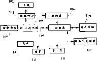
图1是适用于本发明的选择呼叫接收机的方块图;Figure 1 is a block diagram of a selective call receiver suitable for use in the present invention;
图2是按照本发明的最佳实施例实现Zero-IF接收机的图1所示的选择呼叫接收机的部分方块图;Figure 2 is a partial block diagram of the selective call receiver shown in Figure 1 implementing a Zero-IF receiver in accordance with a preferred embodiment of the present invention;
图3是按照本发明的第二实施例实现双转换接收机的图1所示的选择呼叫接收机的部分方块图;FIG. 3 is a partial block diagram of the selective calling receiver shown in FIG. 1 implementing a double conversion receiver according to a second embodiment of the present invention;
图4是按照本发明最佳实施例的具有可控的输出功率的射频放大器的方块图;4 is a block diagram of a radio frequency amplifier with controllable output power according to a preferred embodiment of the present invention;
图5是按照本发明最佳实施例供射频放大器利用的射频电平检测器的简化电路图。Figure 5 is a simplified circuit diagram of an RF level detector for use with an RF amplifier in accordance with a preferred embodiment of the present invention.
参见图1,由电池101供电的选择呼叫接收机通过天线102接收信号。接收部分103把接收信号耦连于解调器104,它使用常规技术恢复收到的任何信息。被恢复的信息信号耦连于控制器105,对其中所含的信息进行译码。在最佳实施例中,控制器105包括以硬件和软件实现的具有信号处理器(例如译码器)的微处理器。Referring to FIG. 1, a selective calling receiver powered by a
恢复的信息被译码器检查,译码器构成信号处理器,用于用预定的地址和恢复的地址相关。非易失存储器107一般具有多个寄存器,用于存储预定地址和表征选择呼叫接收机的操作的多个配置字。在确定选择呼叫接收机的选择时,使含在信息信号内的恢复的地址和相应于选择呼叫接收机的预定地址之间相互关连。当地址基本上相关时,则发出表示选择呼叫接收机的选择的检测信号,并且控制器105把译码的消息信息耦连于消息存储器106。支持电路108按照恢复的信息、和用户控制装置109有关的配置及检测信号进行操作,处理消息信息中的至少一部分,用于例如通过显示器110进行显示,可以通过听觉或触觉报警装置111通知用户消息已经收到。通过启动合适的控制装置109,用户可以看到现在显示器110上的信息。The recovered information is checked by a decoder constituting a signal processor for correlating the recovered address with a predetermined address. The
支持电路108最好包括常规的信号多路复用集成电路,以及可以向支持电路108、接收部分103、解调器104或选择呼叫接收机其它元件提供调节电压的电压调节器。另外,支持电路可以被集成地耦连于控制器(例如微控制器,包括A/D、D/A转换器,可编程的I/O端口,控制总线等等)。此外,支持电路可以包括环境检测电路,例如用于检测光和温度条件,音频功率放大器电路,控制接口电路,时钟频率合成器、以及显示照明电路。这些元件以常规方式构成,用于按用户要求为接收机提供信息显示。
现在参见图2,图2的部分方块图说明按照本发明第一实施例的图1所示的选择呼叫接收机中的Zero-IF接收部分。Referring now to FIG. 2, FIG. 2 is a partial block diagram illustrating a Zero-IF receiving section in the selective call receiver shown in FIG. 1 according to a first embodiment of the present invention.
接收的信号从天线102被耦连于RF放大器202。RF放大器202具有可控的输出功率,所述输出功率至少部分地由和接收信号相关的检测幅值确定。当检测的幅值超过预定幅值时,前馈电平限制器201就把控制信号耦连于RF放大器202,借以调节RF放大器202的可控的输出功率,并防止由高输入信号电平引起失真。预定幅值应当这样选择,使得有用信号在这样一个信噪比或载波噪声比(噪声指的是任何不想要的或无用的信号)下被放大,从而使得产生的信号质量对实现常规的无线电信号电路的无差错译码是可以接受的。用这种方式其中可能含有调制的载波信号的接收信号将被清楚地放大,并保持良好的状态以便随后进行译码。The received signal is coupled from
在初次放大之后,接收信号被使用常规的频率转换器203下变换为基带信号。所得的基带信号接着利用常规的Zero-IF解调器204解调,例如利用微分与交叉相乘拓扑结构或类似电路。所述转换通过接收的信号和由可控的频率合成器205或常规的晶体控制振荡器(未示出)提供的本地振荡信号进行混合来实现。在最佳实施例中,可控频率合成器205例如包括可编程的锁相环合成器206,以及下述部分中的至少一个:常规的除以N的预定标器、双模除法器或N等分电路,使得本地振荡信号频率可以按粗的或细的增量按步增加。可控频率合成器205还可以被用于合成与构成选择呼叫接收机的其它部分(例如译码器)相关的时钟数字逻辑电路所需要的任何数量的频率。After the initial amplification, the received signal is down converted to baseband using a conventional frequency converter 203 . The resulting baseband signal is then demodulated using a conventional Zero-IF demodulator 204, for example using a differential and cross-multiply topology or similar. The conversion is accomplished by mixing the received signal with a local oscillator signal provided by a
可控频率合成器205响应控制模块(例如由Motorola,Inc.制造的MC68HC05C4)105,进行一系列决定和随后要详细说明的控制作用。控制模块105通过在可控频率合成器205中写入一个控制字(例如一个除数)来调节本地振荡器信号频率,从而把锁相环206编程为目标频率。所述控制字由频率参考元件207和所需的输出频率之间的关系导出。所述关系可以是预先确定的,并把其参数存储在非易失存储器107中。然后,非易失存储器107可以被控制器105访问,从而对可编程的锁相环合成器206的输出频率编程。A
作为另一个例子,考虑二次(无用的)射频信号被天线102接收并和有用信号一道加到RF放大器202上的情况。在这种情况下,可能引起高电平或互调失真(IMD)。高电平失真和互调失真的术语虽然不同,但都可被可相互轮换地使用,用来说明和非线性失真有关的放大器所涉及的下述问题。因为由器件产生的IMD的电平和与器件有关的非线性有很大关系,并且一般来说减少增益可使器件操作线性化,所以可通过检测输入电平(在RF放大器202的输入端)和输出电平(在RF放大器的输出端),以及如果可能的话,检测接收信号的中间频率(IF)相对电平指示来控制IMD。响应检测这些电平之一,RF放大器的增益被调整,从而在放大有用信号时实现并保持RF放大器的线性操作。在有源器件例如放大器的情况下,减少不想要的信号的输入电平一般会使在有用的接收信号中的失真相应地减少。As another example, consider the case where a secondary (unwanted) radio frequency signal is received by
本发明尤其适用于减少失真同时又以前馈调节方式操作。响应与在RF放大器202的输入端存在的接收信号相关的检测的幅值,调整RF放大器202的输出功率,以无条件的稳定方式实现前馈调整。这种操作大大减少了和现有技术的增益控制系统例如用正或负反馈进行操作的系统相关的复杂性,这是因为,在本发明中不用补偿可达到稳定。The invention is particularly useful for reducing distortion while operating in a feed-forward regulation manner. Adjusting the output power of the RF amplifier 202 in response to the detected magnitude associated with the received signal present at the input of the RF amplifier 202 implements feed-forward regulation in an unconditionally stable manner. This operation greatly reduces the complexity associated with prior art gain control systems such as those operating with positive or negative feedback, since in the present invention stabilization is achieved without compensation.
可以采用许多方法减少接收部分103中出现的不想要的信号电平。用于控制在转换部分例如基带转换器中的失真的另一种方法在名称为“具有控制互调失真的自适应收发机的通信系统”的Edward T.Clark发明的并转让给Motorola,In.c的5,001,766的美国专利中披露了。在此把其中的教导列为参考。这一美国专利在其第一实施例中讨论了一种测量接收信号的质量的一种装置。当质量于一个预定的品质因数时,就进行调节用于实现射频信号,从第一频率向第二频率转换的本地振荡信号的驱动电平。Clark专利还讨论了一种调节射频放大器的增益从而防止信号过载的任选的控制装置。此外,Clark讨论了一种用于控制发送射频信号的装置的传输功率的编码响应的交换机。在第二实施例中,Clark讨论了一种确定接收信号的相对信号强度的RSSI检测器。然后,响应检测的信号质量和相对信号强度,控制器使所述射频放大器的增益和本地振荡器驱动电平相适应。The unwanted signal level present in the receiving
本领域的技术人员可以理解,Clark披露的方法和装置通过增加本发明优点可以进一步改善。Those skilled in the art will appreciate that the methods and apparatus disclosed by Clark can be further improved by adding the advantages of the present invention.
参见图3,所示的方块图说明按照本发明第二实施例在图1所示的选择呼叫接收机中实现的频率合成双转换接收部分。Referring to FIG. 3, there is shown a block diagram illustrating a frequency synthesis double conversion receiving section implemented in the selective calling receiver shown in FIG. 1 according to a second embodiment of the present invention.
接收的信号,从天线102通过匹配电路301耦连于RF放大器302。RF放大器302具有可控的输出功率,所述输出功率至少部分地被与接收的信号有关的检测幅值确定。当幅值超过预定值时,前馈电平限制器201把控制信号耦连于RF放大器302,借以调整RF放大器302的可控的输出功率,并阻止由于高输入信号电平而产生的失真。按照图2中的例子,预定的幅值应是这样选择,使得有用信号在这样一个信噪比或载波噪声比(噪声指的是任何不想要的或无用的信号)下被放大,使得产生的信号质量对实现常规的无线电信号电路的无差错译码是可以接受的。用这种方式,其中可能含有调制的载波信号的接收信号将被清楚地放大,并保持良好的状态以便随后进行译码。The received signal is coupled from the
这种例子的双转换接收部分“RF前端”301,302,303,304,305以现有技术中熟知的方式响应通过天线102接收并耦合的传输信号。从天线102接收的信号呆以任选地使用已知技术被预先处理,从而提供在预定带宽内耦连于第一混合器304的最佳信号、电平。The double-conversion receive section "RF front end" 301, 302, 303, 304, 305 of this example responds to the transmission signal received and coupled through the
接收信号的可选择的预处理通常由匹配电路301,射频放大器302以及预选器滤波电路303进行,这些电路的设计和功能是本领域的熟知的。匹配电路301使天线10的阻抗特性和RF放大器302相匹配。最好设计匹配电路以便提供具有最佳噪声匹配(最小的噪声)和低的介入损耗的RF放大器302,借以使从天线102向RF放大器302输送的接收信号功率为最佳。然后,放大的信号被耦连于预选择器滤波电路303,它以最小的衰减接收有用信号(例如在预定的频带内),并衰减(即排斥)所有无用信号。这样,接收的信号被预处理并被耦连于第一信号混合器304。Optional preprocessing of the received signal is typically performed by matching circuit 301,
然后第一混合器304混合预处理的接收信号和由可控频率合成器203提供的第一本地振荡注入信号。可控频率合成器具有从频率参考元件207导出的输出频率。所进行的转换产生第一中频信号,然后把其耦连于晶体滤波器305,该滤波器使第一中频信号通过,而使任何不用的信号例如第一混合器图象信号和第一本地振荡器注入信号衰减。The
第二混合器306混合第一中频信号和由可控频率完成器205提供的第二本地振荡器注入信号。所得的第二中频信号被特定地滤波和放大(即通过中频放大与滤波电路307)并被耦连于解调器104。在本实施例中的解调器包括调制检测器308,调制检测器308以本领域熟知的方式恢复通过数据滤波器309耦连于译码器的信息(即FSK数字数据,音频音,PSK数字数据,SSB等)。The
在进行频率选择时,控制器106被耦连于包括锁相环206的可控频率合成器205。控制器进行操作以便执行微编码程序,用于产生频率控制信号。频率控制信号用于对可控频率合成器205的输出频率编程,以便反映相对于所需的操作频率(例如本地振荡频率,时钟频率等)基本上为百万分之零的频率误差。For frequency selection, the
非易失存储器(例如只读存储器,备份随机访问存储,EEPROM等)107用于存储可执行的控制器指令,存储用于表示编程的输出频率和其相应的控制字(例如分频系数)的表,并存储所需的非易失配置信息,用于完成在控制过程中的决定和控制作用,下文将详细说明。Non-volatile memory (such as read-only memory, backup random access storage, EEPROM, etc.) 107 is used to store executable controller instructions, and stores the code used to represent the programmed output frequency and its corresponding control word (such as frequency division coefficient) table, and store the required non-volatile configuration information, which is used to complete the decision and control role in the control process, which will be described in detail below.
参见图4,所示的方块图表示具有按照本发明的最佳实施例的可控的输出功率值的射频放大器。Referring to FIG. 4, a block diagram is shown representing a radio frequency amplifier having controllable output power levels in accordance with a preferred embodiment of the present invention.
当来自天线102的信号强度低于接收机的预定的信号过载电平时,RF电平检测器500的差动输出将不减少RF放大器202的电流消耗。当来自天线的信号强度超过过载电平时,RF电平检测器500的差动输出将变为其另一种不对称状态。在这种状态下,RF放大器202的电流消耗和由此导致的功率增益随着天线信号强度的增加而减少。结果,RF放大器202的输出功率将相对保持恒定。The differential output of the
低通滤波器401,402进行操作用来基本上除去交流信号分量并通过RF电平检测器500输出的直流信号分量。这种操作阻止两个接近的频率的不同的分量到达放大器电流控制部分403,并阻止对RF放大器202进行幅值调制。The low pass filters 401, 402 operate to substantially remove the AC signal component and the DC signal component output by the
放大器电流控制电路403使用合适的常规的差动缓冲器/放大器或类似电路实现。放大器电流控制电路403的功能是响应由RF电平检测器500和低通滤波器401,402检测并滤波的直流值,通过根据检测的信号强度调节可为RF放大器202利用的电流值来控制RF放大器202的功率增益。Amplifier current control circuit 403 is implemented using a suitable conventional differential buffer/amplifier or similar circuit. The function of amplifier current control circuit 403 is to control RF by adjusting the current value available to RF amplifier 202 according to the detected signal strength in response to the DC value detected and filtered by
在操作方面,差动RF电平检测器500变为非对称状态时的RF电压具有极好的重复性。因为转换门限基本上由用于制造差动电平检测器的晶体管的面积比(area ratio)确定,即使在用于制造元件的集成电路工艺变化时,和预定幅值有关的检测门限也将基本保持恒定不变。而且,因为使用差动信号控制电流和RF放大器202的有效输出功率,所以可以确保在工艺和温度改变时具有良好的重复性。In terms of operation, the RF voltage at which the differential
参见图5,其中简化的电路图表示供本发明的最佳实施例的射频放大器使用的射频电平检测器。Referring to Fig. 5, there is shown a simplified circuit diagram showing a radio frequency level detector for use with the radio frequency amplifier of the preferred embodiment of the present invention.
差动RF电平检测器500实际上是一种非对称地加偏压的差动放大器。Q2501的面积因数(area factor)被设计得大于Q1502的面积因数,因此,由于在Q1502的基极不存在RF电压,所以端子LPF-1 503的电压比端子LPF-2 504的电压高。当Q1502的基极上的RF电压增加时,Q1502的集电极电流将由于“Δ(delta)电流”现象而增加。通常用百分数表示的Δ电流是在每个放大级中的静态直流工作电流和加有RF的级的工作电流之间的差。工作电流的增加主要是由于当RF被施加时有源器件的整流和滤波效果,例如,双极晶体管具有二极管、电阻以及和器件有关的电容,其功能类似于用于检测作为直流值的RF能量的平均值的电路。因而,通过产生有效的直流值检测有效的RF电压。Differential
使Q1502的集电极电流等于Q2501的集电极电流所需的RF电压被Q2501和Q1502之间的面积因数差确定。因而,因Q2501比Q1502的面积因数较大,所以在Q1502的基极上需要加较大的RF电压才能达到相等的集电极电流。随着RF电压进一步增加,Q1502的集电极电流将超过Q2501的集电极电流,从而使得LPF-2504比LPF-1502处于较高的电位上。然后所得的差动电压(VLPF-2,VLPF-1)通过把滤波的差动电压耦连到放大器电流控制电路403被用于控制RF放大器的增益。The RF voltage required to make the collector current ofQ1 502 equal to the collector current ofQ2 501 is determined by the difference in area factor betweenQ2 501 andQ1 502 . Therefore, becauseQ2 501 has a larger area factor thanQ1 502, a larger RF voltage needs to be applied to the base ofQ1 502 to achieve equal collector current. As the RF voltage increases further, the collector current ofQ1 502 will exceed the collector current ofQ2 501 , thereby placing LPF-2504 at a higher potential than LPF-1502. The resulting differential voltages (VLPF-2 , VLPF-1 ) are then used to control the gain of the RF amplifier by coupling the filtered differential voltage to the amplifier current control circuit 403 .
关于差动RF电平检测器500的静态直流工作点,用基本上等于1伏的直流电压516向电路供电。电阻R1510,R2511,R3515,R4513,R5514,R6519以及R7512用来对于合适的操作提供稳态直流偏压。正如对称差动放大器的情况一样,左右两边元件基本上彼此相等。在本例中,如上所述,除去晶体管Q1502和Q2501之外,左右两边的元件彼此相等。电容C1作为交流耦合阻抗,用来允许检测在射频放大器202收到的输入信号电平。电容C2作为RF旁路电容,用来使RF电平检测器500的性能基本上和频率无关。电容C3和C4形成交流短路,保证RF电平检测器在RF频率上没有或具有很小的增益。这些电容还用来增加Q1502的输入阻抗,使之和天线102匹配。With respect to the quiescent DC operating point of the differential
总之,这里说明的本发明最好被在图1所示的选择呼叫接收机中进行实施,其中含有输出功率电平为可控的射频放大器202、302。射频电平检测器500响应在射频放大器202,302接收的输入信号电平产生检测器输出信号。检测器输出信号具有包括复合的周期与非周期分量的频谱成分。然后把该信号耦连于至少一个滤波器401,402,例如对其进行调整的低通滤波器,使得产生代表在射频放大器存在的接收输入信号电平的有效值的滤波器输出信号或控制信号。然后把控制信号耦连于放大器输出功率值调整电路403,以无条件稳定前馈方式调节射频放大器202,302的功率增益,使得当由射频电平检测器500检测的接收输入信号电平达到或超过预定的信号过载电平时,输出功率值基本维持恒定。In summary, the invention described herein is preferably implemented in a selective call receiver as shown in FIG. 1, which includes
更具体地说,射频电平检测器500包括具有两个半个差动部分的单端输入的差动输出放大器。射频电平检测器当从射频放大器202,302耦连的接收输入信号电平低于预定的信号过载电平时在第一状态操作,使得两个半个差动部分沿第一非对称方向偏置,从而不进行输出功率值的调节,因而允许输出功率值基本上跟随接收输入信号电平;而当接收的输入信号电平达到或超过预定信号过载电平时,在第二状态操作,使得两个差动部分沿第二非对称方向偏置,从而产生差动输出信号,该信号影响射频放大器的功率增益的调节,使得维持基本上恒定的射频放大器输出功率值。而且,放大器输出功率值调节电路403还可以响应接收的信道上的信号的相对强度指示(如图2,3和4中所示的RSSI信号),使得放大器输出功率值调节电路进行操作,从而调节射频放大器202的功率增益,使得当接收的信道上(on-channel)的信号达到或超过预定信号过载值时,输出功率值维持恒定。More specifically,
最后,为方便起见,射频放大器202,302,射频是平检测器500,至少一个滤波器401,402,以及放大器输出功率值调节电路403被制造在一个集成电路内。Finally, for convenience, the
本领域的普通技术人员可以理解,根据所披露的发明可以作出不同的改变,应当允许用不同方式达到同一目的。这些改变的例子可能有只把披露的电路部分集成在一片集成电路中,或由于实际设计中对例如射频干扰之类的考虑而把某些元件有目的地分开。此外,所述的接收,解调和译码技术当然都是例子,没有理由排除其它技术,例如非常规的调制与信号处理方法,如扩展频谱,或使用数字选择、检测和译码方法。Those skilled in the art will appreciate that various changes can be made in accordance with the disclosed invention, which should allow different ways to achieve the same purpose. Examples of these changes may include integrating only part of the disclosed circuit into an integrated circuit, or separating certain components purposefully due to considerations such as radio frequency interference in actual design. Furthermore, the reception, demodulation and decoding techniques described are of course examples and there is no reason to exclude other techniques such as unconventional modulation and signal processing methods such as spread spectrum, or the use of digital selection, detection and decoding methods.
Claims (18)
Translated fromChineseApplications Claiming Priority (2)
| Application Number | Priority Date | Filing Date | Title |
|---|---|---|---|
| US08/334,092US5564092A (en) | 1994-11-04 | 1994-11-04 | Differential feed-forward amplifier power control for a radio receiver system |
| US08/334,092 | 1994-11-04 |
Publications (2)
| Publication Number | Publication Date |
|---|---|
| CN1162375Atrue CN1162375A (en) | 1997-10-15 |
| CN1096756C CN1096756C (en) | 2002-12-18 |
Family
ID=23305539
Family Applications (1)
| Application Number | Title | Priority Date | Filing Date |
|---|---|---|---|
| CN95196024AExpired - LifetimeCN1096756C (en) | 1994-11-04 | 1995-11-03 | Differential feed-forward amplifier power control circuit of radio receiver system |
Country Status (6)
| Country | Link |
|---|---|
| US (3) | US5564092A (en) |
| EP (1) | EP0807338A4 (en) |
| JP (1) | JPH10513017A (en) |
| KR (1) | KR970707645A (en) |
| CN (1) | CN1096756C (en) |
| WO (1) | WO1996014693A1 (en) |
Cited By (2)
| Publication number | Priority date | Publication date | Assignee | Title |
|---|---|---|---|---|
| CN104579390A (en)* | 2014-02-17 | 2015-04-29 | 上海奎信微电子技术有限公司 | ASK (Amplitude Shift Keying) wireless receiver and automatic gain control method thereof |
| CN110868234A (en)* | 2018-08-08 | 2020-03-06 | 韦伯斯特生物官能(以色列)有限公司 | Contact force sensor including tuned amplifier |
Families Citing this family (57)
| Publication number | Priority date | Publication date | Assignee | Title |
|---|---|---|---|---|
| US5564092A (en)* | 1994-11-04 | 1996-10-08 | Motorola, Inc. | Differential feed-forward amplifier power control for a radio receiver system |
| US5722063A (en)* | 1994-12-16 | 1998-02-24 | Qualcomm Incorporated | Method and apparatus for increasing receiver immunity to interference |
| US6236863B1 (en)* | 1997-03-31 | 2001-05-22 | Oki Telecom, Inc. | Comprehensive transmitter power control system for radio telephones |
| US5923217A (en)* | 1997-06-27 | 1999-07-13 | Motorola, Inc. | Amplifier circuit and method for generating a bias voltage |
| GB2335119A (en)* | 1997-08-20 | 1999-09-08 | Motorola Inc | Self configuring multi-mode communications terminal |
| US6078793A (en)* | 1997-11-06 | 2000-06-20 | Motorola Inc. | High precision controlled gain voice processing system and method |
| KR100241780B1 (en)* | 1997-12-16 | 2000-02-01 | 윤종용 | Power saving apparatus for radio communication terminal |
| JPH11220346A (en)* | 1998-02-02 | 1999-08-10 | Fujitsu Ltd | Automatic gain control circuit |
| US6442216B1 (en)* | 1998-03-04 | 2002-08-27 | Motorola, Inc. | Digital demodulator using boxcar filters and boxcar filter sections |
| US6137372A (en)* | 1998-05-29 | 2000-10-24 | Silicon Laboratories Inc. | Method and apparatus for providing coarse and fine tuning control for synthesizing high-frequency signals for wireless communications |
| US6993314B2 (en) | 1998-05-29 | 2006-01-31 | Silicon Laboratories Inc. | Apparatus for generating multiple radio frequencies in communication circuitry and associated methods |
| US6574288B1 (en) | 1998-05-29 | 2003-06-03 | Silicon Laboratories Inc. | Method and apparatus for adjusting a digital control word to tune synthesized high-frequency signals for wireless communications |
| US6147567A (en)* | 1998-05-29 | 2000-11-14 | Silicon Laboratories Inc. | Method and apparatus for providing analog and digitally controlled capacitances for synthesizing high-frequency signals for wireless communications |
| US6226506B1 (en) | 1998-05-29 | 2001-05-01 | Silicon Laboratories, Inc. | Method and apparatus for eliminating floating voltage nodes within a discreetly variable capacitance used for synthesizing high-frequency signals for wireless communications |
| US7035607B2 (en)* | 1998-05-29 | 2006-04-25 | Silicon Laboratories Inc. | Systems and methods for providing an adjustable reference signal to RF circuitry |
| US6304146B1 (en) | 1998-05-29 | 2001-10-16 | Silicon Laboratories, Inc. | Method and apparatus for synthesizing dual band high-frequency signals for wireless communications |
| US6167245A (en)* | 1998-05-29 | 2000-12-26 | Silicon Laboratories, Inc. | Method and apparatus for operating a PLL with a phase detector/sample hold circuit for synthesizing high-frequency signals for wireless communications |
| US7221921B2 (en)* | 1998-05-29 | 2007-05-22 | Silicon Laboratories | Partitioning of radio-frequency apparatus |
| US7024221B2 (en)* | 2001-01-12 | 2006-04-04 | Silicon Laboratories Inc. | Notch filter for DC offset reduction in radio-frequency apparatus and associated methods |
| US6233441B1 (en) | 1998-05-29 | 2001-05-15 | Silicon Laboratories, Inc. | Method and apparatus for generating a discretely variable capacitance for synthesizing high-frequency signals for wireless communications |
| US7242912B2 (en)* | 1998-05-29 | 2007-07-10 | Silicon Laboratories Inc. | Partitioning of radio-frequency apparatus |
| US6150891A (en) | 1998-05-29 | 2000-11-21 | Silicon Laboratories, Inc. | PLL synthesizer having phase shifted control signals |
| US7228109B2 (en)* | 2001-01-12 | 2007-06-05 | Silicon Laboratories Inc. | DC offset reduction in radio-frequency apparatus and associated methods |
| US6308055B1 (en)* | 1998-05-29 | 2001-10-23 | Silicon Laboratories, Inc. | Method and apparatus for operating a PLL for synthesizing high-frequency signals for wireless communications |
| US6327463B1 (en) | 1998-05-29 | 2001-12-04 | Silicon Laboratories, Inc. | Method and apparatus for generating a variable capacitance for synthesizing high-frequency signals for wireless communications |
| US6804497B2 (en) | 2001-01-12 | 2004-10-12 | Silicon Laboratories, Inc. | Partitioned radio-frequency apparatus and associated methods |
| US7092675B2 (en)* | 1998-05-29 | 2006-08-15 | Silicon Laboratories | Apparatus and methods for generating radio frequencies in communication circuitry using multiple control signals |
| US6311050B1 (en)* | 1998-05-29 | 2001-10-30 | Silicon Laboratories, Inc. | Single integrated circuit phase locked loop for synthesizing high-frequency signals for wireless communications and method for operating same |
| US6970717B2 (en) | 2001-01-12 | 2005-11-29 | Silicon Laboratories Inc. | Digital architecture for radio-frequency apparatus and associated methods |
| FI982561A7 (en) | 1998-11-26 | 2000-05-27 | Nokia Corp | Power control method and power control system |
| US7171176B1 (en)* | 1998-12-30 | 2007-01-30 | Microtune (Texas), L.P. | Tuner system self adaptive to signal environment |
| US6229998B1 (en) | 1999-04-12 | 2001-05-08 | Qualcomm Inc. | Method and system for detecting in-band jammers in a spread spectrum wireless base station |
| DE50006837D1 (en)* | 1999-08-10 | 2004-07-22 | Siemens Ag | METHOD AND ARRANGEMENT FOR OPERATING AN RF POWER AMPLIFIER |
| JP4014072B2 (en)* | 2000-03-31 | 2007-11-28 | 株式会社ルネサステクノロジ | Power amplifier module |
| US6323735B1 (en) | 2000-05-25 | 2001-11-27 | Silicon Laboratories, Inc. | Method and apparatus for synthesizing high-frequency signals utilizing on-package oscillator circuit inductors |
| US6903617B2 (en) | 2000-05-25 | 2005-06-07 | Silicon Laboratories Inc. | Method and apparatus for synthesizing high-frequency signals for wireless communications |
| EP1170860A1 (en)* | 2000-06-27 | 2002-01-09 | Nortel Matra Cellular | Improved multi-carrier receiver for radio telecommunications network |
| JP2002118483A (en) | 2000-10-11 | 2002-04-19 | Matsushita Electric Ind Co Ltd | Radio circuit device and control method thereof |
| US7138858B2 (en) | 2001-01-12 | 2006-11-21 | Silicon Laboratories, Inc. | Apparatus and methods for output buffer circuitry with constant output power in radio-frequency circuitry |
| US7158574B2 (en)* | 2001-01-12 | 2007-01-02 | Silicon Laboratories Inc. | Digital interface in radio-frequency apparatus and associated methods |
| US7031683B2 (en)* | 2001-01-12 | 2006-04-18 | Silicon Laboratories Inc. | Apparatus and methods for calibrating signal-processing circuitry |
| US20030232613A1 (en)* | 2001-01-12 | 2003-12-18 | Kerth Donald A. | Quadrature signal generation in radio-frequency apparatus and associated methods |
| US7035611B2 (en)* | 2001-01-12 | 2006-04-25 | Silicon Laboratories Inc. | Apparatus and method for front-end circuitry in radio-frequency apparatus |
| US7177610B2 (en)* | 2001-01-12 | 2007-02-13 | Silicon Laboratories Inc. | Calibrated low-noise current and voltage references and associated methods |
| US6534966B2 (en)* | 2001-05-10 | 2003-03-18 | Linear Technology Corporation | Methods and apparatus for power measuring receiver |
| US6586996B2 (en)* | 2001-08-15 | 2003-07-01 | Broadcom Corporation | Method and system for producing a drive signal for a current steering amplifier |
| US6614303B2 (en)* | 2001-08-17 | 2003-09-02 | Nokia Mobile Phones, Ltd. | Signal dependent current controlled amplifier and method of performing same |
| US6985698B2 (en)* | 2001-11-14 | 2006-01-10 | Koninklijke Philips Electronics N.V. | Impedeance matching circuit for a multi-band radio frequency device |
| US20030096588A1 (en)* | 2001-11-20 | 2003-05-22 | Vanderhelm Ronald J. | Receiver intermod enhancer |
| AU2003220281A1 (en)* | 2002-03-15 | 2003-09-29 | Silicon Laboratories Inc. | Radio-frequency apparatus and associated methods |
| US20050205986A1 (en)* | 2004-03-18 | 2005-09-22 | Ikuroh Ichitsubo | Module with integrated active substrate and passive substrate |
| DE102006046403A1 (en)* | 2006-09-29 | 2008-04-03 | Robert Bosch Gmbh | Circuit arrangement for micromechanical sensor element, has circuit arrangement comprising circuit units which generate control signal which is decoupled from utility signal of capacitor arrangement |
| RU2342775C1 (en)* | 2007-05-29 | 2008-12-27 | Открытое акционерное общество "Концерн "Созвездие" | Narrow-band radio set |
| GB0816571D0 (en) | 2008-09-10 | 2008-10-15 | Cambridge Silicon Radio Ltd | Automatic gain control & DC offset compensation |
| US8451376B1 (en)* | 2012-04-24 | 2013-05-28 | Silicon Laboratories Inc. | Automatic gain control (AGC) for analog TV signals using feed-forward signal path delay |
| GB2560045B (en)* | 2017-02-28 | 2019-10-30 | Cirrus Logic Int Semiconductor Ltd | Amplifiers |
| US11054481B2 (en) | 2019-03-19 | 2021-07-06 | Battelle Energy Alliance, Llc | Multispectral impedance determination under dynamic load conditions |
Family Cites Families (15)
| Publication number | Priority date | Publication date | Assignee | Title |
|---|---|---|---|---|
| US3821649A (en)* | 1973-02-15 | 1974-06-28 | Gte Sylvania Inc | Signal strength meter circuitry |
| US3918003A (en)* | 1974-10-29 | 1975-11-04 | Bell Telephone Labor Inc | Combined feedback and feedforward automatic gain control |
| GB1545623A (en)* | 1976-05-19 | 1979-05-10 | Elap | Transmission system and repeater stations therefor |
| US4169219A (en)* | 1977-03-30 | 1979-09-25 | Beard Terry D | Compander noise reduction method and apparatus |
| FR2452208A1 (en)* | 1979-03-20 | 1980-10-17 | Thomson Csf | HEAD HEAD WITH SELF-ADAPTIVE DYNAMIC AND RECEIVER COMPRISING SUCH A HEAD |
| JPS57155816A (en)* | 1981-03-20 | 1982-09-27 | Fujitsu Ltd | Automatic gain control circuit |
| US4811423A (en)* | 1986-12-23 | 1989-03-07 | Motorola, Inc. | SSB receiver with improved feedforward AGC |
| US5001776A (en)* | 1988-10-27 | 1991-03-19 | Motorola Inc. | Communication system with adaptive transceivers to control intermodulation distortion |
| US5012140A (en)* | 1990-03-19 | 1991-04-30 | Tektronix, Inc. | Logarithmic amplifier with gain control |
| JPH04103207A (en)* | 1990-08-22 | 1992-04-06 | Mitsubishi Electric Corp | Automatic power controller for linear modulation wave |
| US5307512A (en)* | 1991-06-03 | 1994-04-26 | Motorola, Inc. | Power control circuitry for achieving wide dynamic range in a transmitter |
| JP2725480B2 (en)* | 1991-06-25 | 1998-03-11 | 日本電気株式会社 | Radio selective call receiver |
| JPH0549058A (en)* | 1991-08-16 | 1993-02-26 | Fujitsu Ltd | Resource matching processing system |
| US5359607A (en)* | 1991-11-13 | 1994-10-25 | Motorola, Inc. | Adaptive intermodulation control |
| US5564092A (en)* | 1994-11-04 | 1996-10-08 | Motorola, Inc. | Differential feed-forward amplifier power control for a radio receiver system |
- 1994
- 1994-11-04USUS08/334,092patent/US5564092A/ennot_activeExpired - Lifetime
- 1995
- 1995-03-07USUS08/400,226patent/US5535444A/ennot_activeExpired - Fee Related
- 1995-11-03KRKR1019970702973Apatent/KR970707645A/ennot_activeAbandoned
- 1995-11-03JPJP8515520Apatent/JPH10513017A/enactivePending
- 1995-11-03WOPCT/US1995/014601patent/WO1996014693A1/ennot_activeApplication Discontinuation
- 1995-11-03EPEP95939865Apatent/EP0807338A4/ennot_activeWithdrawn
- 1995-11-03CNCN95196024Apatent/CN1096756C/ennot_activeExpired - Lifetime
- 1995-12-14USUS08/572,140patent/US5740524A/ennot_activeExpired - Lifetime
Cited By (3)
| Publication number | Priority date | Publication date | Assignee | Title |
|---|---|---|---|---|
| CN104579390A (en)* | 2014-02-17 | 2015-04-29 | 上海奎信微电子技术有限公司 | ASK (Amplitude Shift Keying) wireless receiver and automatic gain control method thereof |
| CN104579390B (en)* | 2014-02-17 | 2017-07-07 | 上海奎信微电子技术有限公司 | ASK wireless receivers and its auto gain control method |
| CN110868234A (en)* | 2018-08-08 | 2020-03-06 | 韦伯斯特生物官能(以色列)有限公司 | Contact force sensor including tuned amplifier |
Also Published As
| Publication number | Publication date |
|---|---|
| US5564092A (en) | 1996-10-08 |
| CN1096756C (en) | 2002-12-18 |
| KR970707645A (en) | 1997-12-01 |
| EP0807338A1 (en) | 1997-11-19 |
| US5740524A (en) | 1998-04-14 |
| EP0807338A4 (en) | 1999-09-15 |
| WO1996014693A1 (en) | 1996-05-17 |
| US5535444A (en) | 1996-07-09 |
| JPH10513017A (en) | 1998-12-08 |
Similar Documents
| Publication | Publication Date | Title |
|---|---|---|
| CN1162375A (en) | Differential feed-forward amplifier power control circuit of radio receiver system | |
| US7196579B2 (en) | Gain-controlled amplifier, receiver circuit and radio communication device | |
| KR100567709B1 (en) | Receiving apparatus | |
| JP2515681B2 (en) | Receiver with automatic frequency control | |
| US6980786B1 (en) | Adaptive receiver system that adjusts to the level of interfering signals | |
| US20060146956A1 (en) | RF transmitter for efficiently compensating output power variation due to temperature and process | |
| JP2996170B2 (en) | Gain control circuit | |
| JPH07336283A (en) | Linear receiver | |
| KR19980079871A (en) | Apparatus and method for controlling the frequency characteristics of a filter | |
| KR100751434B1 (en) | Single tone detection and adaptive gain control for direct conversion receivers | |
| US5422911A (en) | Frequency walled phase lock loop | |
| US6943618B1 (en) | Compensation mechanism for compensating bias levels of an operation circuit in response to supply voltage changes | |
| US20090058552A1 (en) | High-frequency module, and mobile telephone and electronic device provided therewith | |
| US20040063408A1 (en) | Low noise linear transmitter using cartesian feedback | |
| CN1701512B (en) | VCO device | |
| US5481226A (en) | Low-voltage intermediate frequency amplifier providing automatic gain control of a source amplifier | |
| US20050093608A1 (en) | DC-offset transient response cancel system | |
| JP2007074230A (en) | Tuner circuit and digital broadcast receiver | |
| US20070147554A1 (en) | Receiver and transmitter/receiver | |
| HK1049926A1 (en) | Wideband voltage controlled oscillator with good noise immunity | |
| US20040043729A1 (en) | Am receiver with audio filtering means | |
| KR100353450B1 (en) | Apparatus and method for improving reception performance and high dynamic range in mobile communication terminal devices | |
| JP3005472B2 (en) | Receiving machine | |
| US7471074B2 (en) | Re-referencing a reference voltage | |
| JPH0349482Y2 (en) |
Legal Events
| Date | Code | Title | Description |
|---|---|---|---|
| C06 | Publication | ||
| PB01 | Publication | ||
| C10 | Entry into substantive examination | ||
| SE01 | Entry into force of request for substantive examination | ||
| C14 | Grant of patent or utility model | ||
| GR01 | Patent grant | ||
| ASS | Succession or assignment of patent right | Owner name:MOTOROLA MOBILE CO., LTD. Free format text:FORMER OWNER: MOTOROLA INC. Effective date:20101230 | |
| C41 | Transfer of patent application or patent right or utility model | ||
| TR01 | Transfer of patent right | Effective date of registration:20101230 Address after:Illinois Instrunment Patentee after:Motorola Mobility LLC Address before:Illinois Instrunment Patentee before:Motorola Inc. | |
| CX01 | Expiry of patent term | Granted publication date:20021218 | |
| EXPY | Termination of patent right or utility model |