CN116209302A - Display panel, manufacturing method thereof and terminal equipment - Google Patents
Display panel, manufacturing method thereof and terminal equipmentDownload PDFInfo
- Publication number
- CN116209302A CN116209302ACN202210297302.4ACN202210297302ACN116209302ACN 116209302 ACN116209302 ACN 116209302ACN 202210297302 ACN202210297302 ACN 202210297302ACN 116209302 ACN116209302 ACN 116209302A
- Authority
- CN
- China
- Prior art keywords
- area
- display panel
- layer structure
- organic layer
- rigid substrate
- Prior art date
- Legal status (The legal status is an assumption and is not a legal conclusion. Google has not performed a legal analysis and makes no representation as to the accuracy of the status listed.)
- Pending
Links
Images


Classifications
- H—ELECTRICITY
- H10—SEMICONDUCTOR DEVICES; ELECTRIC SOLID-STATE DEVICES NOT OTHERWISE PROVIDED FOR
- H10K—ORGANIC ELECTRIC SOLID-STATE DEVICES
- H10K59/00—Integrated devices, or assemblies of multiple devices, comprising at least one organic light-emitting element covered by group H10K50/00
- H10K59/10—OLED displays
- H10K59/12—Active-matrix OLED [AMOLED] displays
- H10K59/131—Interconnections, e.g. wiring lines or terminals
- G—PHYSICS
- G02—OPTICS
- G02F—OPTICAL DEVICES OR ARRANGEMENTS FOR THE CONTROL OF LIGHT BY MODIFICATION OF THE OPTICAL PROPERTIES OF THE MEDIA OF THE ELEMENTS INVOLVED THEREIN; NON-LINEAR OPTICS; FREQUENCY-CHANGING OF LIGHT; OPTICAL LOGIC ELEMENTS; OPTICAL ANALOGUE/DIGITAL CONVERTERS
- G02F1/00—Devices or arrangements for the control of the intensity, colour, phase, polarisation or direction of light arriving from an independent light source, e.g. switching, gating or modulating; Non-linear optics
- G02F1/01—Devices or arrangements for the control of the intensity, colour, phase, polarisation or direction of light arriving from an independent light source, e.g. switching, gating or modulating; Non-linear optics for the control of the intensity, phase, polarisation or colour
- G02F1/13—Devices or arrangements for the control of the intensity, colour, phase, polarisation or direction of light arriving from an independent light source, e.g. switching, gating or modulating; Non-linear optics for the control of the intensity, phase, polarisation or colour based on liquid crystals, e.g. single liquid crystal display cells
- G02F1/133—Constructional arrangements; Operation of liquid crystal cells; Circuit arrangements
- G02F1/1333—Constructional arrangements; Manufacturing methods
- G02F1/133305—Flexible substrates, e.g. plastics, organic film
- G—PHYSICS
- G02—OPTICS
- G02F—OPTICAL DEVICES OR ARRANGEMENTS FOR THE CONTROL OF LIGHT BY MODIFICATION OF THE OPTICAL PROPERTIES OF THE MEDIA OF THE ELEMENTS INVOLVED THEREIN; NON-LINEAR OPTICS; FREQUENCY-CHANGING OF LIGHT; OPTICAL LOGIC ELEMENTS; OPTICAL ANALOGUE/DIGITAL CONVERTERS
- G02F1/00—Devices or arrangements for the control of the intensity, colour, phase, polarisation or direction of light arriving from an independent light source, e.g. switching, gating or modulating; Non-linear optics
- G02F1/01—Devices or arrangements for the control of the intensity, colour, phase, polarisation or direction of light arriving from an independent light source, e.g. switching, gating or modulating; Non-linear optics for the control of the intensity, phase, polarisation or colour
- G02F1/13—Devices or arrangements for the control of the intensity, colour, phase, polarisation or direction of light arriving from an independent light source, e.g. switching, gating or modulating; Non-linear optics for the control of the intensity, phase, polarisation or colour based on liquid crystals, e.g. single liquid crystal display cells
- G02F1/133—Constructional arrangements; Operation of liquid crystal cells; Circuit arrangements
- G02F1/1333—Constructional arrangements; Manufacturing methods
- G02F1/133302—Rigid substrates, e.g. inorganic substrates
- G—PHYSICS
- G02—OPTICS
- G02F—OPTICAL DEVICES OR ARRANGEMENTS FOR THE CONTROL OF LIGHT BY MODIFICATION OF THE OPTICAL PROPERTIES OF THE MEDIA OF THE ELEMENTS INVOLVED THEREIN; NON-LINEAR OPTICS; FREQUENCY-CHANGING OF LIGHT; OPTICAL LOGIC ELEMENTS; OPTICAL ANALOGUE/DIGITAL CONVERTERS
- G02F1/00—Devices or arrangements for the control of the intensity, colour, phase, polarisation or direction of light arriving from an independent light source, e.g. switching, gating or modulating; Non-linear optics
- G02F1/01—Devices or arrangements for the control of the intensity, colour, phase, polarisation or direction of light arriving from an independent light source, e.g. switching, gating or modulating; Non-linear optics for the control of the intensity, phase, polarisation or colour
- G02F1/13—Devices or arrangements for the control of the intensity, colour, phase, polarisation or direction of light arriving from an independent light source, e.g. switching, gating or modulating; Non-linear optics for the control of the intensity, phase, polarisation or colour based on liquid crystals, e.g. single liquid crystal display cells
- G02F1/133—Constructional arrangements; Operation of liquid crystal cells; Circuit arrangements
- G02F1/1333—Constructional arrangements; Manufacturing methods
- G02F1/1345—Conductors connecting electrodes to cell terminals
- G02F1/13452—Conductors connecting driver circuitry and terminals of panels
- H—ELECTRICITY
- H10—SEMICONDUCTOR DEVICES; ELECTRIC SOLID-STATE DEVICES NOT OTHERWISE PROVIDED FOR
- H10K—ORGANIC ELECTRIC SOLID-STATE DEVICES
- H10K59/00—Integrated devices, or assemblies of multiple devices, comprising at least one organic light-emitting element covered by group H10K50/00
- H10K59/10—OLED displays
- H10K59/12—Active-matrix OLED [AMOLED] displays
- H10K59/1201—Manufacture or treatment
- H—ELECTRICITY
- H10—SEMICONDUCTOR DEVICES; ELECTRIC SOLID-STATE DEVICES NOT OTHERWISE PROVIDED FOR
- H10K—ORGANIC ELECTRIC SOLID-STATE DEVICES
- H10K59/00—Integrated devices, or assemblies of multiple devices, comprising at least one organic light-emitting element covered by group H10K50/00
- H10K59/10—OLED displays
- H10K59/12—Active-matrix OLED [AMOLED] displays
- H10K59/124—Insulating layers formed between TFT elements and OLED elements
- Y—GENERAL TAGGING OF NEW TECHNOLOGICAL DEVELOPMENTS; GENERAL TAGGING OF CROSS-SECTIONAL TECHNOLOGIES SPANNING OVER SEVERAL SECTIONS OF THE IPC; TECHNICAL SUBJECTS COVERED BY FORMER USPC CROSS-REFERENCE ART COLLECTIONS [XRACs] AND DIGESTS
- Y02—TECHNOLOGIES OR APPLICATIONS FOR MITIGATION OR ADAPTATION AGAINST CLIMATE CHANGE
- Y02E—REDUCTION OF GREENHOUSE GAS [GHG] EMISSIONS, RELATED TO ENERGY GENERATION, TRANSMISSION OR DISTRIBUTION
- Y02E10/00—Energy generation through renewable energy sources
- Y02E10/50—Photovoltaic [PV] energy
- Y02E10/549—Organic PV cells
Landscapes
- Physics & Mathematics (AREA)
- Nonlinear Science (AREA)
- Chemical & Material Sciences (AREA)
- Engineering & Computer Science (AREA)
- Optics & Photonics (AREA)
- General Physics & Mathematics (AREA)
- Crystallography & Structural Chemistry (AREA)
- Mathematical Physics (AREA)
- Microelectronics & Electronic Packaging (AREA)
- Inorganic Chemistry (AREA)
- Manufacturing & Machinery (AREA)
- Devices For Indicating Variable Information By Combining Individual Elements (AREA)
- Electroluminescent Light Sources (AREA)
Abstract
Translated fromChinese
Description
Translated fromChinese本申请为2021年11月29日递交的申请号为202111428818.X的发明申请《显示面板及其制作方法、终端设备》的分案申请。This application is a divisional application of the invention application "display panel and its manufacturing method, and terminal equipment" with application number 202111428818.X submitted on November 29, 2021.
技术领域technical field
本申请涉及终端技术领域,尤其涉及一种显示面板及其制作方法、终端设备。The present application relates to the technical field of terminals, in particular to a display panel, a manufacturing method thereof, and a terminal device.
背景技术Background technique
随着信息时代的不断发展,手机等终端设备已成为人们生活和工作中较为常用的工具,并且,随着用户对终端设备的要求越来越高,窄边框的终端设备逐渐受到用户的青睐,使得窄边框的终端设备逐渐成为行业追逐的趋势。With the continuous development of the information age, terminal devices such as mobile phones have become more commonly used tools in people's life and work, and as users have higher and higher requirements for terminal devices, terminal devices with narrow borders are gradually favored by users. The terminal equipment with narrow frame has gradually become the trend pursued by the industry.
但是,针对终端设备中的刚性显示面板,由于其需要在周边区设置驱动芯片等结构,导致刚性显示面板的绑定区所在侧的边框宽度较大。However, for the rigid display panel in the terminal device, since it needs to arrange structures such as a driver chip in the peripheral area, the frame width of the side where the binding area of the rigid display panel is located is relatively large.
发明内容Contents of the invention
本申请实施例提供一种显示面板及其制作方法、终端设备,以减小刚性显示面板的绑定区所在侧的边框宽度。Embodiments of the present application provide a display panel, a manufacturing method thereof, and a terminal device, so as to reduce a border width of a rigid display panel on a side where a binding region is located.
第一方面,本申请实施例提出一种显示面板,该显示面板具有显示区和围绕显示区的边框区,边框区包括第一周边区、弯折区和绑定区,第一周边区、弯折区和绑定区依次远离显示区设置,绑定区通过弯折区弯折至显示面板的背光侧;该显示面板包括:刚性衬底、设置在刚性衬底上的驱动电路层,以及依次远离刚性衬底设置的第一有机层结构、导电层和第二有机层结构;刚性衬底和驱动电路层避开弯折区设置;第一有机层结构、导电层和第二有机层结构,至少分布在第一周边区、弯折区和绑定区,第一周边区处的第一有机层结构位于驱动电路层远离刚性衬底的一侧。In the first aspect, the embodiment of the present application provides a display panel, the display panel has a display area and a frame area surrounding the display area, the frame area includes a first peripheral area, a bending area and a binding area, the first peripheral area, the bending area The folding area and the binding area are set away from the display area in turn, and the binding area is bent to the backlight side of the display panel through the bending area; the display panel includes: a rigid substrate, a driving circuit layer arranged on the rigid substrate, and sequentially The first organic layer structure, the conductive layer and the second organic layer structure arranged away from the rigid substrate; the rigid substrate and the driving circuit layer are arranged away from the bending area; the first organic layer structure, the conductive layer and the second organic layer structure, Distributed at least in the first peripheral region, the bending region and the binding region, the first organic layer structure at the first peripheral region is located on the side of the driving circuit layer away from the rigid substrate.
这样,通过将弯折区处的刚性衬底和驱动电路层剥离,使得弯折区处的显示面板可以进行弯折,从而使得绑定区处的显示面板可以弯折至显示面板的背光侧,以减小显示面板绑定区所在侧的边框宽度;并且,在第一周边区、弯折区和绑定区内设置第一有机层结构、第一无机层结构、导电层和第二有机层结构,可加强弯折区处的显示面板的刚性,以更好地维持弯折区处的弯折形貌;另外,由于驱动电路层在弯折区处避开设置,因此,通过导电层可以将驱动电路层中的信号线与绑定区处的驱动芯片连接,以使得驱动芯片输出的信号可以传输至信号线。In this way, by peeling off the rigid substrate and the driving circuit layer at the bending area, the display panel at the bending area can be bent, so that the display panel at the binding area can be bent to the backlight side of the display panel, To reduce the frame width of the side where the binding area of the display panel is located; and, a first organic layer structure, a first inorganic layer structure, a conductive layer and a second organic layer are arranged in the first peripheral area, the bending area and the binding area The structure can strengthen the rigidity of the display panel at the bending area to better maintain the bending shape at the bending area; in addition, since the driving circuit layer is avoided at the bending area, the conductive layer can The signal lines in the driving circuit layer are connected to the driving chip at the bonding area, so that the signals output by the driving chip can be transmitted to the signal lines.
在一种可选的实施方式中,显示面板还包括设置在第一有机层结构与导电层之间的第一无机层结构;第一无机层结构包括至少一层无机层,且第一无机层结构至少分布在第一周边区、弯折区和绑定区。这样,可通过设置第一无机层结构阻隔水氧,减少水氧对导电层中的连接引线造成的侵蚀。In an optional implementation manner, the display panel further includes a first inorganic layer structure disposed between the first organic layer structure and the conductive layer; the first inorganic layer structure includes at least one inorganic layer, and the first inorganic layer The structures are distributed at least in the first peripheral area, the bending area and the binding area. In this way, water and oxygen can be blocked by arranging the first inorganic layer structure, so as to reduce the corrosion caused by water and oxygen to the connection leads in the conductive layer.
在一种可选的实施方式中,边框区还包括第二周边区、第三周边区和第四周边区,第一周边区与第三周边区位于显示区相对的两侧,第二周边区和第四周边区均位于第一周边区与第三周边区之间,且第二周边区与第四周边区也位于显示区相对的两侧;第一有机层结构和第一无机层结构还分布在显示区、第二周边区、第三周边区和第四周边区。这样,通过在显示面板的各个区域均设置第一有机层结构和第一无机层结构,可降低第一有机层结构和第一无机层结构在图案化处理时的工艺复杂度,并且,该第一有机层结构和第一无机层结构也可以同时作为显示区内的绝缘膜层,以减少显示区内需要制作的绝缘膜层的数量。In an optional implementation manner, the frame area further includes a second peripheral area, a third peripheral area and a fourth peripheral area, the first peripheral area and the third peripheral area are located on opposite sides of the display area, and the second peripheral area and the fourth peripheral area are located between the first peripheral area and the third peripheral area, and the second peripheral area and the fourth peripheral area are also located on opposite sides of the display area; the first organic layer structure and the first inorganic layer structure are also Distributed in the display area, the second peripheral area, the third peripheral area and the fourth peripheral area. In this way, by arranging the first organic layer structure and the first inorganic layer structure in each region of the display panel, the process complexity of the patterning process of the first organic layer structure and the first inorganic layer structure can be reduced, and the second An organic layer structure and the first inorganic layer structure can also be used as insulating film layers in the display area at the same time, so as to reduce the number of insulating film layers that need to be fabricated in the display area.
在一种可选的实施方式中,导电层包括多条连接引线,连接引线的一端通过贯穿第一无机层结构和第一有机层结构的第一过孔,与驱动电路层中的信号线连接,连接引线的另一端还通过贯穿第二有机层结构的第二过孔,与设置在绑定区的驱动芯片连接。这样,通过连接引线可实现驱动电路层中的信号线与绑定区处的驱动芯片的连接,使得驱动芯片输出的信号可以传输至信号线。In an optional embodiment, the conductive layer includes a plurality of connection leads, and one end of the connection lead is connected to the signal line in the driving circuit layer through the first via hole passing through the first inorganic layer structure and the first organic layer structure. The other end of the connection lead is also connected to the driving chip arranged in the bonding area through the second via hole penetrating through the second organic layer structure. In this way, the connection of the signal line in the driving circuit layer and the driving chip at the bonding area can be realized through the connecting wire, so that the signal output by the driving chip can be transmitted to the signal line.
在一种可选的实施方式中,显示面板为液晶显示器(liquid crystal display,LCD)显示面板,导电层和第二有机层结构避开显示区设置;信号线还延伸至第一周边区,第一过孔位于第一周边区内。这样,通过在显示区内不设置导电层和第二有机层结构,可减少显示区内的膜层的层数,提高显示区处的显示面板的透过率。In an optional implementation manner, the display panel is a liquid crystal display (liquid crystal display, LCD) display panel, and the conductive layer and the second organic layer structure are set away from the display area; the signal line also extends to the first peripheral area, and the second A via hole is located in the first peripheral area. In this way, by not disposing the conductive layer and the second organic layer structure in the display area, the number of film layers in the display area can be reduced, and the transmittance of the display panel at the display area can be improved.
在一种可选的实施方式中,显示面板为有机发光二极管(organic light-emitting diode,OLED)显示面板,导电层和第二有机层结构还分布在显示区;信号线还延伸至第一周边区,第一过孔位于第一周边区内;或者,第一过孔位于显示区内。这样,由于OLED可以自发光,因此,显示区内的导电层和第二有机层结构不会影响显示面板的透过率;并且,当导电层还分布在显示区内时,也可以在显示区处,将驱动电路层中的信号线与绑定区处的驱动芯片进行连接。In an optional embodiment, the display panel is an organic light-emitting diode (organic light-emitting diode, OLED) display panel, and the conductive layer and the second organic layer structure are also distributed in the display area; the signal line also extends to the first periphery area, the first via hole is located in the first peripheral area; or, the first via hole is located in the display area. In this way, since the OLED can emit light by itself, the structure of the conductive layer and the second organic layer in the display area will not affect the transmittance of the display panel; , the signal line in the driving circuit layer is connected to the driving chip at the binding area.
在一种可选的实施方式中,边框区还包括第二周边区、第三周边区和第四周边区,第一周边区与第三周边区位于显示区相对的两侧,第二周边区和第四周边区均位于第一周边区与第三周边区之间,且第二周边区与第四周边区也位于显示区相对的两侧;导电层和第二有机层结构还分布在第二周边区、第三周边区和第四周边区。这样,通过在显示面板的各个区域均设置导电层和第二有机层结构,可降低导电层和第二有机层结构在图案化处理时的工艺复杂度,并且,通过在显示区内增设第二有机层结构,可提高显示区内的膜层的平整度。In an optional implementation manner, the frame area further includes a second peripheral area, a third peripheral area and a fourth peripheral area, the first peripheral area and the third peripheral area are located on opposite sides of the display area, and the second peripheral area and the fourth peripheral area are located between the first peripheral area and the third peripheral area, and the second peripheral area and the fourth peripheral area are also located on opposite sides of the display area; the conductive layer and the second organic layer structure are also distributed in the second peripheral area The second peripheral area, the third peripheral area and the fourth peripheral area. In this way, by arranging the conductive layer and the second organic layer structure in each area of the display panel, the process complexity of the patterning process of the conductive layer and the second organic layer structure can be reduced, and, by adding the second organic layer structure in the display area The organic layer structure can improve the flatness of the film layer in the display area.
在一种可选的实施方式中,第一有机层结构和第二有机层结构均包括至少一层有机层。In an optional embodiment, both the first organic layer structure and the second organic layer structure include at least one organic layer.
在一种可选的实施方式中,第一有机层结构包括多层有机层,显示面板还包括设置在相邻两层有机层之间的第二无机层结构;第二无机层结构包括至少一层无机层,且第二无机层结构至少分布在第一周边区、弯折区和绑定区。这样,通过增设第二无机层结构,可进一步减少水氧对导电层中的连接引线造成的侵蚀,并且可在一定程度上增强弯折区的刚性。In an optional embodiment, the first organic layer structure includes multiple organic layers, and the display panel further includes a second inorganic layer structure disposed between two adjacent organic layers; the second inorganic layer structure includes at least one An inorganic layer, and the second inorganic layer structure is at least distributed in the first peripheral area, the bending area and the binding area. In this way, by adding the second inorganic layer structure, the corrosion caused by water and oxygen to the connection leads in the conductive layer can be further reduced, and the rigidity of the bending region can be enhanced to a certain extent.
在一种可选的实施方式中,该显示面板还包括:阳极层,阳极层分布在显示区,且位于第二有机层结构远离刚性衬底的一侧;像素界定层,像素界定层至少分布在显示区、第一周边区、弯折区和绑定区,且像素界定层位于第二有机层结构远离第一有机层结构的一侧。这样,通过将像素界定层延伸至弯折区,可进一步提高弯折区的刚性。In an optional embodiment, the display panel further includes: an anode layer, distributed in the display area, and located on the side of the second organic layer structure away from the rigid substrate; a pixel defining layer, distributed at least In the display area, the first peripheral area, the bending area and the binding area, the pixel defining layer is located on the side of the second organic layer structure away from the first organic layer structure. In this way, by extending the pixel defining layer to the bending area, the rigidity of the bending area can be further improved.
在一种可选的实施方式中,显示面板还包括粘接层,粘接层位于绑定区处的刚性衬底与显示区处的刚性衬底之间。这样,通过粘接层将绑定区处的刚性衬底与显示区处的刚性衬底粘接,使得绑定区处的膜层结构可以稳定的固定在显示面板的背光侧。In an optional implementation manner, the display panel further includes an adhesive layer, and the adhesive layer is located between the rigid substrate at the binding area and the rigid substrate at the display area. In this way, the rigid substrate at the binding area is bonded to the rigid substrate at the display area through the adhesive layer, so that the film layer structure at the binding area can be stably fixed on the backlight side of the display panel.
第二方面,本申请实施例提出了一种显示面板的制作方法,包括:提供一刚性衬底;刚性衬底被划分为显示区和围绕显示区的边框区,边框区包括第一周边区、弯折区和绑定区,第一周边区、弯折区和绑定区依次远离显示区设置;在刚性衬底上形成驱动电路层;在驱动电路层上依次形成第一有机层结构、导电层和第二有机层结构;第一有机层结构、导电层和第二有机层结构,至少分布在第一周边区、弯折区和绑定区;将弯折区处的刚性衬底和驱动电路层剥离;将弯折区朝向显示面板的背光侧弯折,使得绑定区弯折至显示面板的背光侧。In the second aspect, the embodiment of the present application proposes a method for manufacturing a display panel, including: providing a rigid substrate; the rigid substrate is divided into a display area and a frame area surrounding the display area, and the frame area includes a first peripheral area, The bending area and the binding area, the first peripheral area, the bending area and the binding area are set away from the display area in turn; the driving circuit layer is formed on the rigid substrate; the first organic layer structure, conductive layer and the second organic layer structure; the first organic layer structure, the conductive layer and the second organic layer structure are distributed at least in the first peripheral region, the bending region and the binding region; the rigid substrate and the driving region at the bending region The circuit layer is peeled off; the bending area is bent toward the backlight side of the display panel, so that the binding area is bent to the backlight side of the display panel.
在一种可选的实施方式中,将弯折区处的刚性衬底和驱动电路层剥离,包括:采用遮光治具对刚性衬底远离驱动电路层的一侧进行激光照射,以将弯折区处的刚性衬底和驱动电路层剥离;其中,遮光治具包括遮光区和透光区,透光区与弯折区对应设置,遮光区与弯折区以外的区域对应设置。In an optional implementation manner, peeling the rigid substrate and the driving circuit layer at the bending area includes: using a light-shielding jig to irradiate the rigid substrate on the side away from the driving circuit layer with laser, so as to separate the bending The rigid substrate and the driving circuit layer at the area are peeled off; wherein, the light-shielding fixture includes a light-shielding area and a light-transmitting area, the light-transmitting area is set correspondingly to the bending area, and the light-shielding area is set correspondingly to the area outside the bending area.
在一种可选的实施方式中,将弯折区朝向显示面板的背光侧弯折之前,还包括:在显示区处的刚性衬底远离第一有机层结构一侧的表面上,和/或,绑定区处的刚性衬底远离第一有机层结构一侧的表面上设置粘接层;在将弯折区朝向显示面板的背光侧弯折之后,还包括:将绑定区处的刚性衬底与显示区处的刚性衬底通过粘接层粘接。In an optional implementation manner, before bending the bending region toward the backlight side of the display panel, further includes: on the surface of the rigid substrate at the display region on the side away from the first organic layer structure, and/or , setting an adhesive layer on the surface of the rigid substrate at the binding area away from the first organic layer structure; after bending the bending area toward the backlight side of the display panel, it also includes: placing the rigid substrate at the binding area The substrate is bonded to the rigid substrate at the display area through an adhesive layer.
第三方面,本申请实施例提出了一种终端设备,包括驱动芯片以及上述的显示面板;驱动芯片位于显示面板的绑定区,且驱动芯片通过贯穿显示面板中的第二有机层结构的第二过孔,与显示面板中的连接引线连接。In the third aspect, the embodiment of the present application proposes a terminal device, including a driver chip and the above-mentioned display panel; the driver chip is located in the binding area of the display panel, and the driver chip passes through the second organic layer structure in the display panel Two through holes are connected with the connection leads in the display panel.
第二方面和第三方面的各可能的实现方式,效果与第一方面以及第一方面的可能的设计中的效果类似,在此不再赘述。The effects of the possible implementations of the second aspect and the third aspect are similar to those of the first aspect and the possible designs of the first aspect, and will not be repeated here.
附图说明Description of drawings
图1为相关技术中的柔性显示模组的结构示意图;FIG. 1 is a schematic structural diagram of a flexible display module in the related art;
图2为相关技术中的刚性显示面板的结构示意图;FIG. 2 is a schematic structural diagram of a rigid display panel in the related art;
图3为本申请实施例提供的终端设备的结构示意图;FIG. 3 is a schematic structural diagram of a terminal device provided in an embodiment of the present application;
图4为本申请实施例提供的刚性显示面板的平面示意图;FIG. 4 is a schematic plan view of a rigid display panel provided by an embodiment of the present application;
图5为本申请实施例提供的第一种刚性显示面板的截面示意图;FIG. 5 is a schematic cross-sectional view of the first rigid display panel provided by the embodiment of the present application;
图6为本申请实施例提供的第二种刚性显示面板的截面示意图;FIG. 6 is a schematic cross-sectional view of a second rigid display panel provided by an embodiment of the present application;
图7为本申请实施例提供的第三种刚性显示面板的截面示意图;FIG. 7 is a schematic cross-sectional view of a third rigid display panel provided by an embodiment of the present application;
图8为本申请实施例提供的第四种刚性显示面板的截面示意图;FIG. 8 is a schematic cross-sectional view of a fourth rigid display panel provided by an embodiment of the present application;
图9为本申请实施例提供的一种刚性显示面板的制作方法的流程图;FIG. 9 is a flow chart of a method for manufacturing a rigid display panel provided by an embodiment of the present application;
图10为本申请采用激光剥离技术,剥离弯折区处的刚性衬底和驱动电路层的示意图;FIG. 10 is a schematic diagram of peeling off the rigid substrate and the driving circuit layer at the bending area using laser lift-off technology in the present application;
图11为本申请实施例提供的刚性显示面板在剥离弯折区处的刚性衬底和驱动电路层前的结构示意图;FIG. 11 is a schematic structural view of the rigid display panel provided by the embodiment of the present application before the rigid substrate and the driving circuit layer at the bending area are peeled off;
图12为本申请实施例提供的刚性显示面板在剥离弯折区处的刚性衬底和驱动电路层后的结构示意图。FIG. 12 is a schematic structural view of the rigid display panel provided by the embodiment of the present application after peeling off the rigid substrate and the driving circuit layer at the bending region.
具体实施方式Detailed ways
为了便于清楚描述本申请实施例的技术方案,在本申请的实施例中,采用了“第一”、“第二”等字样对功能和作用基本相同的相同项或相似项进行区分。例如,第一芯片和第二芯片仅仅是为了区分不同的芯片,并不对其先后顺序进行限定。本领域技术人员可以理解“第一”、“第二”等字样并不对数量和执行次序进行限定,并且“第一”、“第二”等字样也并不限定一定不同。In order to clearly describe the technical solutions of the embodiments of the present application, in the embodiments of the present application, words such as "first" and "second" are used to distinguish the same or similar items with basically the same function and effect. For example, the first chip and the second chip are only used to distinguish different chips, and their sequence is not limited. Those skilled in the art can understand that words such as "first" and "second" do not limit the quantity and execution order, and words such as "first" and "second" do not necessarily limit the difference.
需要说明的是,本申请实施例中,“示例性的”或者“例如”等词用于表示作例子、例证或说明。本申请中被描述为“示例性的”或者“例如”的任何实施例或设计方案不应被解释为比其他实施例或设计方案更优选或更具优势。确切而言,使用“示例性的”或者“例如”等词旨在以具体方式呈现相关概念。It should be noted that, in the embodiments of the present application, words such as "exemplary" or "for example" are used as examples, illustrations or descriptions. Any embodiment or design described herein as "exemplary" or "for example" is not to be construed as preferred or advantageous over other embodiments or designs. Rather, the use of words such as "exemplary" or "such as" is intended to present related concepts in a concrete manner.
本申请实施例中,“至少一个”是指一个或者多个,“多个”是指两个或两个以上。“和/或”,描述关联对象的关联关系,表示可以存在三种关系,例如,A和/或B,可以表示:单独存在A,同时存在A和B,单独存在B的情况,其中A,B可以是单数或者复数。字符“/”一般表示前后关联对象是一种“或”的关系。“以下至少一项(个)”或其类似表达,是指的这些项中的任意组合,包括单项(个)或复数项(个)的任意组合。例如,a,b,或c中的至少一项(个),可以表示:a,b,c,a-b,a-c,b-c,或a-b-c,其中a,b,c可以是单个,也可以是多个。In the embodiments of the present application, "at least one" means one or more, and "multiple" means two or more. "And/or" describes the association relationship of associated objects, indicating that there may be three types of relationships, for example, A and/or B, which can mean: A exists alone, A and B exist at the same time, and B exists alone, where A, B can be singular or plural. The character "/" generally indicates that the contextual objects are an "or" relationship. "At least one of the following" or similar expressions refer to any combination of these items, including any combination of single or plural items. For example, at least one item (piece) of a, b, or c can represent: a, b, c, a-b, a-c, b-c, or a-b-c, where a, b, c can be single or multiple .
随着信息时代的不断发展,手机等终端设备已成为人们生活和工作中较为常用的工具,并且,随着用户对终端设备的要求越来越高,窄边框的终端设备逐渐受到用户的青睐,使得窄边框的终端设备逐渐成为行业追逐的趋势。With the continuous development of the information age, terminal devices such as mobile phones have become more commonly used tools in people's life and work, and as users have higher and higher requirements for terminal devices, terminal devices with narrow borders are gradually favored by users. The terminal equipment with narrow frame has gradually become the trend pursued by the industry.
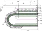
在相关技术中,如图1所示,柔性显示模组包括:柔性显示面板101、第一背膜102、粘接层103、支撑垫104、第二背膜105、金属覆盖层(metal cover layer,MCL)106、封装层107、触控层108、偏光片109、光学胶层110以及盖板111;并且,柔性显示模组被划分为显示区AA和边框区NA,边框区NA包括周边区B1、弯折区B2和绑定区B3,周边区B1指的是显示区AA到封装层107的边界之间的区域。In the related art, as shown in FIG. 1, the flexible display module includes: a
通过采用柔性材料作为柔性显示面板101的衬底材料,使得弯折区B2处的柔性显示面板101可以弯折,则绑定区B3处的柔性显示面板101,可通过弯折区B2处的柔性显示面板101弯折至柔性显示面板101的背光侧,从而减小柔性显示面板101的绑定区B3所在侧的边框宽度。By using a flexible material as the substrate material of the
但是,柔性显示面板101的制作成本通常大于刚性显示面板的制作成本,为了降低终端设备的制作成本,可采用刚性显示面板作为终端设备的显示面板。However, the manufacturing cost of the
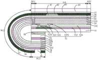
如图2所示,刚性显示面板包括刚性背板21,刚性背板21被划分为显示区AA和边框区NA,边框区NA包括周边区和边缘区B4,周边区包括走线搭接区B11和封装区B12,边缘区B4指的是封装区B12到刚性背板21的边缘之间的区域,且边缘区B4包括用于绑定驱动芯片的绑定区。As shown in FIG. 2 , the rigid display panel includes a
在显示区AA处的刚性背板21上设置有发光器件221等结构,在走线搭接区B11处的刚性背板21上设置有搭接走线等结构222,在封装区B12处的刚性背板21上设置有封装结构223;此外,该刚性显示面板还包括盖板23。Structures such as light-emitting
其中,刚性背板21中的衬底材料为刚性材料,则刚性背板21无法进行弯折,因此会导致刚性显示面板的绑定区所在侧的边框宽度较大。经测试,图2所示的刚性显示面板的边框区NA的宽度一般大于或等于2.3mm,而边缘区B4基本上会占到1.67mm左右。Wherein, the substrate material in the
基于此,本申请实施例提供了一种显示面板,通过将弯折区处的刚性衬底和驱动电路层剥离,使得弯折区处的显示面板可以进行弯折,从而使得绑定区处的显示面板可以弯折至显示面板的背光侧,以减小显示面板绑定区所在侧的边框宽度;并且,在第一周边区、弯折区和绑定区内设置第一有机层结构、第一无机层结构、导电层和第二有机层结构,可加强弯折区处的显示面板的刚性,以更好地维持弯折区处的弯折形貌;另外,由于驱动电路层在弯折区处避开设置,为了使得驱动电路层中的信号线可以与绑定区处的驱动芯片连接,可通过导电层将信号线与驱动芯片连接,以使得驱动芯片输出的信号可以传输至信号线,且还可以通过第一无机层结构减少水氧对导电层中的连接引线的侵蚀。Based on this, an embodiment of the present application provides a display panel. By peeling off the rigid substrate and the driving circuit layer at the bending area, the display panel at the bending area can be bent, so that the bonding area The display panel can be bent to the backlight side of the display panel, so as to reduce the frame width of the side where the binding area of the display panel is located; and, the first organic layer structure, the second An inorganic layer structure, a conductive layer and a second organic layer structure can strengthen the rigidity of the display panel at the bending area to better maintain the bending shape at the bending area; in addition, since the driving circuit layer is bending Avoid setting at the area, in order to make the signal lines in the driving circuit layer can be connected to the driving chip at the binding area, the signal line can be connected to the driving chip through the conductive layer, so that the signal output by the driving chip can be transmitted to the signal line , and the corrosion of the connecting wires in the conductive layer by water and oxygen can also be reduced through the structure of the first inorganic layer.
本申请实施例提供的显示面板,可以应用在具备显示功能的终端设备中,该终端设备可以是手机、平板电脑、电子阅读器、笔记本电脑、车载设备、可穿戴设备、电视等需要设置成窄边框的设备。The display panel provided by the embodiment of the present application can be applied to a terminal device with a display function. Border device.
本申请实施例以终端设备为手机为例进行说明。如图3所示,终端设备300包括显示面板30和壳体40。其中,显示面板30为刚性显示面板,显示面板30安装于壳体40上,其用于显示图像或视频等;显示面板30和壳体40共同围设出终端设备300的容纳腔体,以便通过该容纳腔体放置终端设备300的电子器件等,同时对位于容纳腔体内的电子器件形成密封和保护的作用。The embodiment of the present application is described by taking the terminal device as a mobile phone as an example. As shown in FIG. 3 , a terminal device 300 includes a
其中,如图4所示,显示面板30具有显示区AA和围绕显示区AA的边框区NA,边框区NA包括第一周边区N11、弯折区N12和绑定区N13,第一周边区N11、弯折区N12和绑定区N13依次远离显示区AA设置,即沿着显示区AA指向绑定区N13的方向上,显示面板30的各区域依次为显示区AA、第一周边区N11、弯折区N12和绑定区N13。Wherein, as shown in FIG. 4 , the
在一些实施例中,第一周边区N11、弯折区N12和绑定区N13位于显示区AA的其中一侧;当然,在显示区AA的至少两侧,也可以设置有第一周边区N11、弯折区N12和绑定区N13。In some embodiments, the first peripheral area N11, the bending area N12 and the binding area N13 are located on one side of the display area AA; of course, the first peripheral area N11 may also be provided on at least two sides of the display area AA , bending region N12 and binding region N13.
第一周边区N11指的是显示区AA与弯折区N12之间的区域。由于在实际产品中,需要在显示面板30的显示区AA的外围,通过封框胶或者封装膜层等封装结构进行封装,以及需要将显示区AA内的信号线与外围引线进行搭接等,因此,第一周边区N11可以包括封装结构所占用的区域,以及显示区AA内的信号线与外围引线的搭接区域等。The first peripheral area N11 refers to the area between the display area AA and the bending area N12. Because in actual products, it is necessary to package the periphery of the display area AA of the
当第一周边区N11、弯折区N12和绑定区N13位于显示区AA的其中一侧时,边框区NA还包括第二周边区N21、第三周边区N31和第四周边区N41,第一周边区N11与第三周边区N31位于显示区AA相对的两侧,第二周边区N21和第四周边区N41均位于第一周边区N11与第三周边区N31之间,且第二周边区N21与第四周边区N41也位于显示区AA相对的两侧。When the first peripheral area N11, the bending area N12, and the binding area N13 are located on one side of the display area AA, the border area NA further includes a second peripheral area N21, a third peripheral area N31, and a fourth peripheral area N41. A peripheral area N11 and the third peripheral area N31 are located on opposite sides of the display area AA, the second peripheral area N21 and the fourth peripheral area N41 are both located between the first peripheral area N11 and the third peripheral area N31, and the second peripheral area The area N21 and the fourth peripheral area N41 are also located on opposite sides of the display area AA.
例如,第一周边区N11、弯折区N12和绑定区N13可以位于显示区AA的下侧,第三周边区N31位于显示区AA的上侧,第二周边区N21位于显示区AA的左侧,第四周边区N41位于显示区AA的右侧。For example, the first peripheral area N11, the bending area N12 and the binding area N13 may be located on the lower side of the display area AA, the third peripheral area N31 is located on the upper side of the display area AA, and the second peripheral area N21 is located on the left side of the display area AA. On the right side of the display area AA, the fourth peripheral area N41 is located on the right side of the display area AA.
下面以四种不同的结构实施方式,说明本申请实施例中的刚性显示面板的具体结构。图5至图8所示的显示面板30的结构,为图4所示的显示面板30将绑定区N13弯折至显示面板30的背光侧后,沿截面C-C’得到的剖视图。The specific structure of the rigid display panel in the embodiment of the present application will be described below in four different structural implementation manners. The structure of the
在第一种可选的实施方式中,如图5所示,显示面板30包括刚性衬底31、驱动电路层32,以及层叠设置的第一有机层结构33、第一无机层结构34、导电层35和第二有机层结构36。In the first optional implementation manner, as shown in FIG. 5 , the
其中,刚性衬底31避开弯折区N12设置,即刚性衬底31分布在显示区AA、第一周边区N11、绑定区N13、第二周边区N21、第三周边区N31和第四周边区N41,刚性衬底31在弯折区N12所在的位置断开设置。Wherein, the
位于显示区AA、第一周边区N11、第二周边区N21、第三周边区N31和第四周边区N41的刚性衬底31为一体结构,其包括相对设置的第一表面和第二表面,以及设置在第一表面与第二表面之间且首尾连接的第一侧面、第二侧面、第三侧面和第四侧面,第一侧面为第一周边区N11所在的侧面,第二侧面为第二周边区N21所在的侧面,第三侧面为第三周边区N31所在的侧面,第四侧面为第四周边区N41所在的侧面。The
位于绑定区N13的刚性衬底31为一体结构,其包括相对设置的第三表面和第四表面,以及设置在第三表面与第四表面之间且首尾连接的第五侧面、第六侧面、第七侧面和第八侧面。在绑定区N13通过弯折区N12弯折至显示面板30的背光侧之前,第四表面与第一表面位于同一平面,第三表面与第二表面位于同一平面,第七侧面与第一侧面相对设置,且第五侧面位于第七侧面远离第一周边区N11的一侧,弯折区N12也就是第一侧面与第七侧面之间的区域。在绑定区N13通过弯折区N12弯折至显示面板30的背光侧之后,第一表面与第四表面相对设置,且第三表面位于第四表面远离第一表面的一侧,第二表面位于第一表面远离第四表面的一侧,而第七侧面与第一侧面可以位于同一平面。显示面板30的背光侧也就指的是刚性衬底31的第一表面所在的一侧。The
刚性衬底31可以为玻璃衬底或者聚甲基丙烯酸甲酯(polymethyl methacrylate,PMMA)衬底等,PMMA衬底也可称为亚克力衬底。The
在位于显示区AA、第一周边区N11、第二周边区N21、第三周边区N31和第四周边区N41的刚性衬底31的第二表面上,以及在位于绑定区N13的刚性衬底31的第三表面上,均设置有驱动电路层32。驱动电路层32避开弯折区N12设置,即驱动电路层32分布在显示区AA、第一周边区N11、绑定区N13、第二周边区N21、第三周边区N31和第四周边区N41,驱动电路层32在弯折区N12所在的位置断开设置。On the second surface of the
在本申请实施例中,该显示面板30可以为OLED显示面板,则位于显示区AA的OLED显示面板30实际上包括多个子像素,每个子像素包括像素驱动电路和发光器件,发光器件设置在像素驱动电路远离刚性衬底31的一侧,且与像素驱动电路连接,像素驱动电路能够提供驱动电压至发光器件,以控制该发光器件的发光状态。因此,位于显示区AA的驱动电路层32实际上指的是,显示区AA内的各个子像素对应的像素驱动电路。In the embodiment of the present application, the
需要说明的是,像素驱动电路的结构包括多种,例如,像素驱动电路的结构可以为6T1C像素驱动电路、7T1C像素驱动电路以及3T1C像素驱动电路等,“T”表示像素驱动电路中的晶体管,位于“T”前面的数字表示像素驱动电路中的晶体管的数量,“C”表示像素驱动电路中的存储电容,“C”前面的数字表示像素驱动电路中的存储电容的数量。It should be noted that there are various structures of the pixel driving circuit. For example, the structure of the pixel driving circuit can be 6T1C pixel driving circuit, 7T1C pixel driving circuit, and 3T1C pixel driving circuit. “T” represents a transistor in the pixel driving circuit, The number before "T" indicates the number of transistors in the pixel driving circuit, "C" indicates the storage capacitor in the pixel driving circuit, and the number before "C" indicates the number of storage capacitors in the pixel driving circuit.
而像素驱动电路中的晶体管,是通过层叠设置的有源层321、栅极绝缘层322、栅极层323、层间介质层324和源漏电极层构成的。此时,位于显示区AA的驱动电路层32包括层叠设置的有源层321、栅极绝缘层322、栅极层323、层间介质层324和源漏电极层。针对位于显示区AA的驱动电路层32,有源层321位于刚性衬底31的第二表面,栅极绝缘层322覆盖有源层321和刚性衬底31的第二表面,栅极层323位于栅极绝缘层322远离刚性衬底31的一侧,层间介质层324覆盖栅极层323和栅极绝缘层322,源漏电极层位于层间介质层324远离刚性衬底31的一侧。The transistor in the pixel driving circuit is composed of an
其中,栅极层323包括各个晶体管的栅极,以及EM(发光控制)信号线、栅线、复位信号线等,源漏电极层包括各个晶体管的源极3251和漏极3252,以及数据线和VDD(高电平电源)信号线等。Wherein, the
而第一周边区N11、绑定区N13、第二周边区N21、第三周边区N31和第四周边区N41内的驱动电路层32,实际上指的是驱动电路层32中的绝缘介质层,如驱动电路层32中的栅极绝缘层322和层间介质层324。针对位于绑定区N13的驱动电路层32,栅极绝缘层322位于刚性衬底31的第三表面上,层间介质层324位于栅极绝缘层322远离刚性衬底31的一侧。The driving
图5示出的驱动电路层32中的晶体管为底栅型晶体管,当然,本申请实施例中的驱动电路层32中的晶体管还可以为顶栅型晶体管。另外,驱动电路层32中的栅极层的层数也可以为多层,且相邻两层栅极层之间需要通过栅极绝缘层间隔设置,驱动电路层32中的源漏电极层的层数也可以为多层,且相邻两层源漏电极层之间需要通过层间介质层间隔设置。The transistors in the
在显示区AA、第一周边区N11、第二周边区N21、第三周边区N31、第四周边区N41、弯折区N12以及绑定区N13内,均设置有层叠设置的第一有机层结构33、第一无机层结构34、导电层35和第二有机层结构36。In the display area AA, the first peripheral area N11, the second peripheral area N21, the third peripheral area N31, the fourth peripheral area N41, the bending area N12, and the bonding area N13, there are stacked first organic layers.
在显示区AA、绑定区N13、第一周边区N11、第二周边区N21、第三周边区N31和第四周边区N41内,第一有机层结构33、第一无机层结构34、导电层35和第二有机层结构36依次远离刚性衬底31的第二表面设置。具体的,第一有机层结构33位于驱动电路层32远离刚性衬底31的一侧,第一无机层结构34位于第一有机层结构33远离刚性衬底31的一侧,导电层35位于第一无机层结构34远离刚性衬底31的一侧,第二有机层结构36位于导电层35远离刚性衬底31的一侧。In the display area AA, the bonding area N13, the first peripheral area N11, the second peripheral area N21, the third peripheral area N31 and the fourth peripheral area N41, the first
在显示面板30的弯折区N12弯折前,弯折区N12内的第一有机层结构33、第一无机层结构34、导电层35和第二有机层结构36,依次远离刚性衬底31的第二表面所在的平面设置;在显示面板30的弯折区N12弯折后,弯折区N12内的第一有机层结构33、第一无机层结构34、导电层35和第二有机层结构36,依次远离刚性衬底31的第一侧面设置,即第一有机层结构33与刚性衬底31的第一侧面存在一定的间隔区域,第一无机层结构34位于第一有机层结构33远离刚性衬底31的第一侧面的一侧,导电层35位于第一无机层结构34远离刚性衬底31的第一侧面的一侧,第二有机层结构36位于导电层35远离刚性衬底31的第一侧面的一侧。Before bending in the bending region N12 of the
其中,第一有机层结构33包括一层有机层,该有机层也可称为平坦层,该有机层的材料可以为树脂等有机材料,第一有机层结构33中的有机层的厚度可以为2μm;第一无机层结构34包括一层无机层,该无机层也可称为钝化层,该无机层的材料可以为氧化硅或氮化硅等无机材料;导电层35的材料可以为钛、铝、钼、铜等金属材料;第二有机层结构36也包括一层有机层,该机层也可称为平坦层,该有机层的材料可以为树脂等有机材料,第二有机层结构36中的有机层的厚度可以为2μm。Wherein, the first
导电层35实际上包括多条连接引线,连接引线的一端通过贯穿第一无机层结构34和第一有机层结构33的第一过孔,与驱动电路层32中的信号线连接,连接引线的另一端还通过贯穿第二有机层结构36的第二过孔50,与设置在绑定区N13的驱动芯片(未在图5中示出)连接。The
在实际产品中,驱动芯片可采用COP(chip on panel)固定在显示面板30的绑定区N13,COP指的是直接将驱动芯片绑定在显示面板30上的工艺;当然,可以采用其他方式将驱动芯片固定在显示面板30的绑定区N13,如采用覆晶薄膜(chip on film,COF)或COG(chipon glass)等方式将驱动芯片固定在显示面板30的绑定区N13。In actual products, the driver chip can be fixed on the bonding area N13 of the
因此,在驱动电路层32在弯折区N12处避开设置的情况下,可通过导电层35将驱动芯片与驱动电路层32中的信号线连接,使得驱动芯片输出的信号可以传输至驱动电路层32中的信号线,使得驱动电路层32中的像素驱动电路可以正常工作。Therefore, in the case where the driving
驱动电路层32中的信号线可以为数据线、VDD信号线等,且数据线、VDD信号线是与驱动电路层32中的晶体管的源极连接,因此,在图5中以连接引线通过贯穿的第一过孔与晶体管的源极3251连接,来表示连接引线与驱动电路层32中的信号线的连接关系。The signal line in the
此时,驱动电路层32中的信号线可以仅分布在显示区AA内,则将第一过孔设置显示区AA内,连接引线在显示区AA内,通过贯穿的第一过孔与驱动电路层32中的信号线连接。At this time, the signal lines in the
当然,可以理解的是,第一有机层结构33、第一无机层结构34、导电层35和第二有机层结构36,也可以仅分布在第一周边区N11、弯折区N12和绑定区N13,此时,第一周边区N11处的第一有机层结构33位于驱动电路层32远离刚性衬底31的一侧。或者,导电层35和第二有机层结构36还可以仅分布在第一周边区N11、弯折区N12、绑定区N13、第二周边区N21、第三周边区N31和第四周边区N41,即导电层35和第二有机层结构36仅避开弯折区N12设置。Of course, it can be understood that the first
需要说明的是,弯折区N12处的第一有机层结构33、第一无机层结构34、导电层35和第二有机层结构36,可加强弯折区N12处的显示面板30的刚性,以更好地维持弯折区N12处的弯折形貌,其中,维持弯折区N12处的弯折形貌主要是通过弯折区N12处的有机层结构(即第一有机层结构33和第二有机层结构36)来实现的。并且,在弯折区N12处设置的有机层结构包括第一有机层结构33和第二有机层结构36,而不是仅包括单层的有机层,其目的是两层有机层结构可以更好地支撑弯折区N12,以维持弯折区N12处的弯折形貌,若仅在弯折区N12设置单层的有机层结构,其支撑效果不佳,难以更好地维持弯折区N12处的弯折形貌。It should be noted that the first
而第一有机层结构33、第一无机层结构34、导电层35和第二有机层结构36还延伸至第一周边区N11和绑定区N13,主要是为了使得第一有机层结构33、第一无机层结构34、导电层35和第二有机层结构36,可以正常搭接在第一周边区N11和绑定区N13的驱动电路层32上。若仅在弯折区N12处设置第一有机层结构33、第一无机层结构34、导电层35和第二有机层结构36,在将弯折区N12处的刚性衬底31和驱动电路层32剥离后,弯折区N12处的第一有机层结构33、第一无机层结构34、导电层35和第二有机层结构36会出现断裂,无法维持弯折区N12的形貌。And the first
而弯折区N12、第一周边区N11和绑定区N13内设置的导电层35,主要是为了将驱动电路层32中的信号线与绑定区N13处的驱动芯片连接,使得驱动芯片输出的信号可以通过导电层35传输至信号线。The
而弯折区N12、第一周边区N11和绑定区N13内设置的第一无机层结构34,其主要是为了阻隔水氧,减少水氧对导电层35中的连接引线造成的侵蚀。因此,在一些实施例中,也可以将图5所示的第一无机层结构34去除,使得弯折区N12、第一周边区N11和绑定区N13内依次层叠设置第一有机层结构33、导电层35和第二有机层结构36。The first
在申请实施例中,如图5所示,显示面板30还包括阳极层41、像素界定层37、发光层42、阴极层43和封装层44等结构。In the embodiment of the application, as shown in FIG. 5 , the
阳极层41分布在显示区AA内,且位于第二有机层结构36远离刚性衬底31的一侧。在实际产品中,阳极层41包括每个子像素对应的阳极,且相邻两个子像素之间的阳极断开设置,阳极层41的材料可以为铝、银等金属材料。The
像素界定层37分布在显示区AA、第一周边区N11、弯折区N12和绑定区N13,此时,在绑定区N13处,第二过孔50还贯穿像素界定层37。当然,像素界定层37还可以分布在第二周边区N21、第三周边区N31和第四周边区N41,像素界定层37位于第二有机层结构36远离第一有机层结构33的一侧。并且,在显示区AA内,像素界定层具有多个像素开口,且每个像素开口至少暴露出部分的阳极,该像素界定层37的厚度可以为1.5μm。The
发光层42位于显示区AA内,其具体位于像素界定层37限定出的像素开口内。The
而阴极层43可以分布在显示区AA、第一周边区N11、第二周边区N21、第三周边区N31和第四周边区N41内,其位于像素界定层37远离刚性衬底31的一侧,该阴极层43的材料为具有高透过率的导电材料,如氧化铟锡(indium tin oxides,ITO)等材料。The
阳极层41、发光层42和阴极层43共同构成发光器件,且发光器件发出的光线的出光侧为朝向阴极层43的一侧,因此,采用高透过率的导电材料制作阴极层43,可减少发光器件的发出的光线经过阴极层43造成的损失。The
封装层44可以分布在显示区AA、第一周边区N11、第二周边区N21、第三周边区N31和第四周边区N41内,其位于阴极层43远离刚性衬底31的一侧。The
此时,弯折区N12处的膜层结构包括:层叠设置的第一有机层结构33、第一无机层结构34、导电层35、第二有机层结构36和像素界定层37,且第一有机层结构33、第一无机层结构34、导电层35、第二有机层结构36和像素界定层37依次远离刚性衬底31的第一侧面设置。At this time, the film layer structure at the bending region N12 includes: a stacked first
需要说明的是,显示面板30还可以设置在封装层44远离刚性衬底31一侧的触控层、偏光片、光学胶层以及盖板等结构。It should be noted that the
另外,为了使得弯折区N12处的显示面板30弯折后,显示面板30的结构稳定性,可以在位于绑定区N13处的刚性衬底31与显示区AA处的刚性衬底31之间设置粘接层38,通过粘接层38将绑定区N13处的刚性衬底31与显示区AA处的刚性衬底31进行粘接,使得绑定区N13处的结构可以稳定的固定在显示面板30的背光侧。此时,粘接层38实际上位于显示区AA的刚性衬底31的第一表面,以及绑定区N13处的刚性衬底31的第四表面之间。In addition, in order to ensure the structural stability of the
综上,通过将弯折区N12处的刚性衬底31和驱动电路层32剥离,使得绑定区N13处的显示面板30,可以通过弯折区N12弯折至显示面板30的背光侧,以减小显示面板30的绑定区N13所在侧的边框宽度。另外,通过在第一周边区N11、弯折区N12和绑定区N13内,设置第一有机层结构33、第一无机层结构34、导电层35和第二有机层结构36,在维持弯折区N12处的弯折形貌的同时,使得驱动芯片可以通过导电层35与驱动电路层32中的信号线连接,且可减少水氧对导电层35中的连接引线造成的侵蚀。To sum up, by peeling off the
在第二种可选的实施方式中,如图6所示,显示面板30包括刚性衬底31、驱动电路层32,以及层叠设置的第一有机层结构33、第一无机层结构34、导电层35和第二有机层结构36。In the second optional implementation manner, as shown in FIG. 6 , the
其中,第一有机层结构33包括两层有机层,其分别为第一有机层331和第二有机层332,且第一有机层331和第二有机层332分布在显示区AA、第一周边区N11、第二周边区N21、第三周边区N31、第四周边区N41、弯折区N12以及绑定区N13内。Wherein, the first
在显示区AA、绑定区N13、第一周边区N11、第二周边区N21、第三周边区N31和第四周边区N41内,第二有机层332位于第一有机层331远离刚性衬底31的一侧。而在显示面板30的弯折区N12弯折前,弯折区N12内的第二有机层332位于第一有机层331远离刚性衬底31的第二表面所在的平面,在显示面板30的弯折区N12弯折后,弯折区N12内的第二有机层332位于第一有机层331远离刚性衬底31的第一侧面。In the display area AA, the bonding area N13, the first peripheral area N11, the second peripheral area N21, the third peripheral area N31 and the fourth peripheral area N41, the second
在实际产品中,第一有机层331和第二有机层332的材料可以相同,例如,第一有机层331和第二有机层332的材料均为树脂材料;或者,第一有机层331和第二有机层332的材料也可以不同。第一有机层331和第二有机层332的厚度可以相等,例如,第一有机层331和第二有机层332的厚度均为2μm;或者,第一有机层331和第二有机层332的厚度也可以不相等,本申请实施例对此不作限制。In actual products, the materials of the first
需要说明的是,图5所示的显示面板30与图6所示的显示面板30,其不同之处在于,图5所示的显示面板30中的第一有机层结构33包括一层有机层,而图6所示的显示面板30中的第一有机层结构33包括两层有机层,其余结构基本类似,为避免重复,在此不再赘述。关于刚性衬底31、驱动电路层32、第一有机层结构33、第一无机层结构34、导电层35和第二有机层结构36等膜层的具体结构,可参照第一种可选的实施方式中的描述。It should be noted that the difference between the
当第一有机层结构33包括两层有机层时,可进一步加强弯折区N12处的显示面板30的刚性,以更好地维持弯折区N12处的弯折形貌。When the first
经测试发现,在图6所示的显示面板30中,弯折区N12的宽度可以为0.25mm,第一周边区N11的宽度为0.7mm,该宽度指的是第一周边区N11指向第三周边区N13的方向上的尺寸,则可以使得显示面板30的绑定区N13所在侧的边框宽度减小至0.95mm。It is found through testing that, in the
在第三种可选的实施方式中,如图7所示,显示面板30包括刚性衬底31、驱动电路层32,以及层叠设置的第一有机层331、第二无机层结构39、第二有机层332、第一无机层结构34、导电层35和第二有机层结构36。In a third optional implementation manner, as shown in FIG. 7 , the
此时,第一有机层结构33包括两层有机层,其分别为第一有机层331和第二有机层332,在第一有机层331与第二有机层332之间还设置有第二无机层结构39,第二无机层结构39包括一层无机层,且该第二无机层结构39分布在显示区AA、第一周边区N11、第二周边区N21、第三周边区N31、第四周边区N41、弯折区N12以及绑定区N13内。At this time, the first
当然,在一些实施例中,第二无机层结构39也可以仅分布在第一周边区N11、弯折区N12以及绑定区N13内;而第二无机层结构39中的无机层的数量也可以不局限于1层,第二无机层结构39也可以包括两层无机层或三层无机层等。Certainly, in some embodiments, the second
在另一些实施例中,第一有机层结构33包括的有机层的数量也可以大于2层,此时,可以在任意相邻两层有机层之间均设置第二无机层结构39,或者部分相邻的两层有机层之间设置第二无机层结构39。例如,第一有机层结构33包括三层有机层,其分别为第一有机层331、第二有机层332和第三有机层,在第一有机层331与第二有机层332设置第二无机层结构39,和/或,在第二有机层332与第三有机层之间设置第二无机层结构39。In some other embodiments, the number of organic layers included in the first
如图7所示,以晶体管的源极3251表示驱动电路层32中的信号线,驱动电路层32中的信号线不仅分布在显示区AA,其还延伸至第一周边区N11内,此时,第一过孔可设置在第一周边区N11内,连接引线在第一周边区N11内,通过贯穿的第一过孔与驱动电路层32中的信号线连接。并且,该第一过孔实际上贯穿的是第一无机层结构34、第二有机层332、第二无机层结构39和第一有机层331。As shown in FIG. 7, the
需要说明的是,图7所示的显示面板30与图6所示的显示面板30,其不同之处有两点。其中一个不同之处在于,图6所示的显示面板30中的第一有机层结构33包括第一有机层331和第二有机层332,而图7所示的显示面板30中,除了第一有机层331和第二有机层332外,在第一有机层331与第二有机层332之间还设置有第二无机层结构39;另一个不同之处在于,图6所示的显示面板30中的第一过孔位于显示区AA内,而图7所示的显示面板30中的第一过孔位于第一周边区N11内。其余结构基本类似,为避免重复,在此不再赘述。It should be noted that there are two differences between the
综上,图5至图7所示的显示面板30均为OLED显示面板,而本申请实施例的显示面板也可以为如图8所示的LCD显示面板。To sum up, the
在第四种可选的实施方式中,如图8所示,显示面板30包括刚性衬底31、驱动电路层32,以及层叠设置的第一有机层结构33、第一无机层结构34、导电层35和第二有机层结构36。In a fourth optional implementation manner, as shown in FIG. 8 , a
其中,驱动电路层32也避开弯折区N12设置,位于显示区AA的驱动电路层32实际上指的是,显示区AA内的各个子像素对应的像素晶体管等结构,该像素晶体管的栅极与栅线连接,该像素晶体管的源极与数据线连接,该像素晶体管的漏极与像素电极51连接,其用于在栅线和数据线的作用下,向像素电极51提供像素电压,使得液晶层52内的液晶分子在像素电极51提供的像素电压,以及公共电极提供的公共电压的作用下发生偏转,以实现显示功能。Wherein, the driving
在显示区AA、第一周边区N11、第二周边区N21、第三周边区N31、第四周边区N41、弯折区N12以及绑定区N13内,均设置有层叠设置的第一有机层结构33和第一无机层结构34。在显示区AA、绑定区N13、第一周边区N11、第二周边区N21、第三周边区N31和第四周边区N41内,第一无机层结构34位于第一有机层结构33远离刚性衬底31的第二表面的一侧。In the display area AA, the first peripheral area N11, the second peripheral area N21, the third peripheral area N31, the fourth peripheral area N41, the bending area N12, and the bonding area N13, there are stacked first organic layers.
在显示面板30的弯折区N12弯折前,弯折区N12内的第一有机层结构33和第一无机层结构34,依次远离刚性衬底31的第二表面所在的平面设置;在显示面板30的弯折区N12弯折后,弯折区N12内的第一有机层结构33和第一无机层结构34,依次远离刚性衬底31的第一侧面设置。Before the bending region N12 of the
而导电层35和第二有机层结构36避开显示区AA设置,即导电层35和第二有机层结构36分布在第一周边区N11、第二周边区N21、第三周边区N31、第四周边区N41、弯折区N12以及绑定区N13内。通过将显示区AA内的导电层35和第二有机层结构36去除,可减少显示区AA内的膜层的层数,提高显示区AA处的显示面板30的透过率。The
在第一周边区N11、第二周边区N21、第三周边区N31、第四周边区N41和绑定区N13内,第二有机层结构36位于导电层35远离刚性衬底31的第二表面的一侧。在显示面板30的弯折区N12弯折前,弯折区N12内的导电层35和第二有机层结构36,依次远离刚性衬底31的第二表面所在的平面设置;在显示面板30的弯折区N12弯折后,在弯折区N12内,第二有机层结构36位于导电层35远离刚性衬底31的第一侧面。In the first peripheral region N11, the second peripheral region N21, the third peripheral region N31, the fourth peripheral region N41 and the binding region N13, the second
当然,在一些实施例中,也可以仅在第一周边区N11、弯折区N12以及绑定区N13内设置导电层35和第二有机层结构36。此时,驱动电路层32中的信号线(如数据线等)还延伸至第一周边区N11,第一过孔位于第一周边区N11;在第一周边区N11内,导电层35包括的连接引线贯穿第一无机层结构34和第一有机层结构33的第一过孔,与驱动电路层32中的信号线连接。Of course, in some embodiments, the
可以理解的是,当导电层35还延伸至第二周边区N21、第三周边区N31和第四周边区N41时,第一过孔可以分布在第二周边区N21、第三周边区N31和第四周边区N41中的任意一个或多个区域,对应的信号线也需要延伸至第二周边区N21、第三周边区N31和第四周边区N41中的任意一个或多个区域,在第二周边区N21、第三周边区N31和第四周边区N41中的任意一个或多个区域内,导电层35包括的连接引线贯穿的第一过孔与驱动电路层32中的信号线连接。It can be understood that when the
此外,如图8所示,显示面板30还包括依次远离第一无机层结构34设置的像素电极51、液晶层52、彩膜基板53和盖板54等结构。像素电极51和液晶层52可以仅分布在显示区AA内,彩膜基板53可分布在显示区AA、第一周边区N11、第二周边区N21、第三周边区N31和第四周边区N41,而盖板54除了覆盖显示区AA、第一周边区N11、第二周边区N21、第三周边区N31和第四周边区N41外,还延伸至弯折区N12所在的位置。In addition, as shown in FIG. 8 , the
经测试发现,在图8所示的显示面板中,弯折区N12的宽度可以为0.3mm,第一周边区N11的宽度可以为0.8mm,则可以使得显示面板30的绑定区N13所在侧的边框宽度减小至1.1mm。It is found through testing that in the display panel shown in FIG. 8 , the width of the bending region N12 can be 0.3 mm, and the width of the first peripheral region N11 can be 0.8 mm, so that the side where the binding region N13 of the
综上,可以看出,本申请实施例中的第一有机层结构33可以包括至少一层有机层,相应的,第二有机层结构36也可以包括至少一层有机层,第一无机层结构34包括至少一层无机层。In summary, it can be seen that the first
上述示出了四种不同的显示面板30,其通过将弯折区N12处的刚性衬底31和驱动电路层32剥离,使得绑定区N13处的显示面板30,可以通过弯折区N12弯折至显示面板30的背光侧,以减小显示面板30的绑定区N13所在侧的边框宽度,该显示面板30可以为OLED显示面板或LCD显示面板,当然,在一些产品中,本申请实施例中的显示面板30也可以为量子点发光二极管(quantum dot light emitting diodes,QLED)显示面板。The above shows four
另外,通过在第一周边区N11、弯折区N12和绑定区N13内,设置第一有机层结构33、第一无机层结构34、导电层35和第二有机层结构36,在维持弯折区N12处的弯折形貌的同时,使得驱动芯片可以通过导电层35与驱动电路层32中的信号线连接,且可减少水氧对导电层35中的连接引线造成的侵蚀。In addition, by arranging the first
图9为本申请实施例提供的一种刚性显示面板的制作方法的流程图。参照图9所示,刚性显示面板的制作方法具体可以包括如下步骤:FIG. 9 is a flow chart of a method for manufacturing a rigid display panel provided by an embodiment of the present application. Referring to FIG. 9 , the manufacturing method of the rigid display panel may specifically include the following steps:
步骤901,提供一刚性衬底;刚性衬底被划分为显示区和围绕显示区的边框区,边框区包括第一周边区、弯折区和绑定区,第一周边区、弯折区和绑定区依次远离显示区设置。
步骤902,在刚性衬底上形成驱动电路层。
在本申请实施例中,在刚性衬底31上依次形成有源层321、栅极绝缘层322、栅极层323、层间介质层324和源漏电极层等,从而制作得到驱动电路层32。In the embodiment of the present application, an
步骤903,在驱动电路层上依次形成第一有机层结构、第一无机层结构、导电层和第二有机层结构;第一有机层结构、第一无机层结构、导电层和第二有机层结构,至少分布在第一周边区、弯折区和绑定区。
在本申请实施例中,在刚性衬底31上形成驱动电路层32之后,在驱动电路层32上先形成第一有机层结构33,然后,在第一有机层结构33上形成第一无机层结构34。In the embodiment of the present application, after the
由于后续形成的导电层35包括的连接引线需要通过贯穿第一无机层结构34和第一有机层结构33的第一过孔,驱动电路层32中的信号线连接,因此,在第一有机层结构33上形成第一无机层结构34之后,还需要对第一无机层结构34和第一有机层结构33进行图案化处理,形成贯穿的第一过孔。其中,图案化处理的工艺包括光刻胶涂覆、曝光、显影、刻蚀以及光刻胶剥离等工艺步骤。Since the connecting wires included in the subsequently formed
当然,若第一无机层结构34和第一有机层结构33仅分布在第一周边区N11、弯折区N12和绑定区N13时,在形成第一过孔时,可同时将显示区AA、第二周边区N21、第三周边区N31和第四周边区N41内的第一无机层结构34和第一有机层结构33去除。Of course, if the first
在第一有机层结构33上形成第一无机层结构34之后,在第一无机层结构34远离刚性衬底31的一侧形成导电薄膜,然后,对导电薄膜进行图案化处理,形成包括多条连接引线的导电层35;最后,在导电层35远离刚性衬底31的一侧形成第二有机层结构36。After forming the first
若第二有机层结构36和导电层35仅分布在第一周边区N11、第二周边区N21、第三周边区N31、第四周边区N41、弯折区N12和绑定区N13时,在对导电薄膜进行图案化处理形成导电层35时,需要同时将显示区AA内的导电薄膜去除,并且,在形成第二有机层结构36时,也需要将显示区AA内的第二有机层结构36的材料去除。If the second
需要说明的是,若第一周边区N11、弯折区N12和绑定区N13内不设置第一无机层结构34时,可以在驱动电路层32上依次形成第一有机层结构33、导电层35和第二有机层结构36。以第一有机层结构33的材料为感光型树脂为例,可直接采用曝光显影的方式,形成贯穿第一有机层结构33的第一过孔。It should be noted that, if the first
此外,针对OLED显示面板,在形成第二有机层结构36之后,还需要依次形成阳极层41、像素界定层37、发光层42、阴极层43和封装层44等结构;针对LCD显示面板,在形成第二有机层结构36之后,还需要形成像素电极51,并将彩膜基板53与形成有像素电极51的刚性衬底31对盒,并注入液晶分子形成液晶层52,最后,将盖板54贴合在彩膜基板53远离刚性衬底31的一侧。In addition, for an OLED display panel, after the second
步骤904,将弯折区处的刚性衬底和驱动电路层剥离。
在本申请实施例中,在制作完成显示面板30的各个膜层之后,将弯折区N12处的刚性衬底31和驱动电路层32剥离。In the embodiment of the present application, after each film layer of the
具体的,可采用遮光治具对刚性衬底31远离驱动电路层32的一侧进行激光照射,以将弯折区N12处的刚性衬底31和驱动电路层32剥离。当激光照射到刚性衬底31远离驱动电路层32的一侧时,驱动电路层32中的层间介质层324与第一有机层结构33之间的界面因灰化而发生分离,从而可以将弯折区N12处的刚性衬底31和驱动电路层32,从显示面板30中剥离出去。Specifically, a light-shielding jig can be used to irradiate the
如图10所示,激光剥离(laser lift-off,LLO)设备包括激光源61、衰减器62、光学系统63、反射器件64和遮光治具65。激光源61用于发出激光,衰减器62用于对激光源61发出的激光进行调制,光学系统63用于对衰减器62调制的激光进行整形、匀束等处理,得到均匀且长期稳定的线光束,反射器件64用于将光学系统63处理得到的激光反射至遮光治具65所在的位置。As shown in FIG. 10 , a laser lift-off (laser lift-off, LLO) device includes a
其中,遮光治具65包括遮光区651和透光区652,透光区652与显示面板30的弯折区N12对应设置,遮光区651与弯折区N12以外的区域对应设置,即遮光区651与显示区AA、绑定区N13、第一周边区N11、第二周边区N21、第三周边区N31和第四周边区N41对应设置。Wherein, the light-shielding
因此,可通过遮光治具65对反射器件64发射的激光进行图案化,使得激光可以通过遮光治具65的透光区652,照射至显示面板30的弯折区N12,以弯折区N12处的刚性衬底31和驱动电路层32剥离。而遮光治具65的遮光区651对激光进行遮挡,防止激光照射到显示面板30的显示区AA、绑定区N13、第一周边区N11、第二周边区N21、第三周边区N31和第四周边区N41,而影响显示面板30的性能。Therefore, the laser light emitted by the
图11为显示面板30在剥离弯折区N12处的刚性衬底31和驱动电路层32前的结构示意图,在采用遮光治具65对显示面板30的弯折区N12进行照射后,可去除弯折区N12处的刚性衬底31和驱动电路层32,得到如图12所示的显示面板30。具体的,是将弯折区N12处的刚性衬底31、驱动电路层32中的栅极绝缘层322和层间介质层324剥离。11 is a schematic structural view of the
需要说明的是,如图10所示,在显示面板30的实际制作过程中,是一次性制作多个显示面板30,这多个显示面板30可共同称为母板,然后将母板切割成多个面板组70,该面板组70包括两列显示面板30,每列显示面板30包括多个显示面板30,则将这两列显示面板30的弯折区N12均朝向这两列显示面板30之间的区域设置,因此,在采用遮光治具65对显示面板30的弯折区N12处的刚性衬底31和驱动电路层32进行剥离时,可一次性将面板组70中的所有显示面板的弯折区N12处的刚性衬底31和驱动电路层32均进行剥离。It should be noted that, as shown in FIG. 10 , in the actual manufacturing process of the
当然,也可以采用遮光治具65执行一次激光剥离,对一个显示面板30或一列显示面板30的弯折区N12处的刚性衬底31和驱动电路层32进行剥离。Of course, the light-shielding
在将显示面板30的弯折区N12处的刚性衬底31和驱动电路层32进行剥离之后,将驱动芯片绑定在显示面板30的绑定区N13内。After the
步骤905,将弯折区朝向显示面板的背光侧弯折,使得绑定区弯折至显示面板的背光侧。
在本申请实施例中,在将驱动芯片绑定在显示面板30的绑定区N13内之后,首先,在显示区AA处的刚性衬底31远离第一有机层结构33一侧的表面(即第一表面)上,和/或,绑定区N13处的刚性衬底31远离第一有机层结构33一侧的表面(即第四表面)上设置粘接层38。In the embodiment of the present application, after the driver chip is bound in the binding area N13 of the
然后,将显示面板30的弯折区N12朝向显示面板30的背光侧弯折,将绑定区N13弯折至显示面板30的背光侧,由于显示区AA处的刚性衬底31的第一表面上,和/或绑定区N13处的刚性衬底31的第四表面上设置有粘接层38,通过压合显示面板30,可使得绑定区N13处的刚性衬底31与显示区AA处的刚性衬底31通过粘接层38粘接。Then, the bending area N12 of the
因此,在将图12所示的显示面板30的绑定区N13,通过弯折区N12弯折至显示面板30的背光侧,并将绑定区N13处的刚性衬底31与显示区AA处的刚性衬底31通过粘接层38粘接后,可得到如图5所示的显示面板30。Therefore, when the binding region N13 of the
以上的具体实施方式,对本申请的目的、技术方案和有益效果进行了进一步详细说明,所应理解的是,以上仅为本申请的具体实施方式而已,并不用于限定本申请的保护范围,凡在本申请的技术方案的基础之上,所做的任何修改、等同替换、改进等,均应包括在本申请的保护范围之内。The specific implementation above has further described the purpose, technical solutions and beneficial effects of the application in detail. It should be understood that the above is only a specific implementation of the application and is not used to limit the scope of protection of the application. On the basis of the technical solution of this application, any modification, equivalent replacement, improvement, etc. should be included in the protection scope of this application.
Claims (19)
Translated fromChinesePriority Applications (1)
| Application Number | Priority Date | Filing Date | Title |
|---|---|---|---|
| CN202210297302.4ACN116209302A (en) | 2021-11-29 | 2021-11-29 | Display panel, manufacturing method thereof and terminal equipment |
Applications Claiming Priority (2)
| Application Number | Priority Date | Filing Date | Title |
|---|---|---|---|
| CN202111428818.XACN113851520B (en) | 2021-11-29 | 2021-11-29 | Display panel, manufacturing method thereof and terminal device |
| CN202210297302.4ACN116209302A (en) | 2021-11-29 | 2021-11-29 | Display panel, manufacturing method thereof and terminal equipment |
Related Parent Applications (1)
| Application Number | Title | Priority Date | Filing Date |
|---|---|---|---|
| CN202111428818.XADivisionCN113851520B (en) | 2021-11-29 | 2021-11-29 | Display panel, manufacturing method thereof and terminal device |
Publications (1)
| Publication Number | Publication Date |
|---|---|
| CN116209302Atrue CN116209302A (en) | 2023-06-02 |
Family
ID=78982180
Family Applications (2)
| Application Number | Title | Priority Date | Filing Date |
|---|---|---|---|
| CN202210297302.4APendingCN116209302A (en) | 2021-11-29 | 2021-11-29 | Display panel, manufacturing method thereof and terminal equipment |
| CN202111428818.XAActiveCN113851520B (en) | 2021-11-29 | 2021-11-29 | Display panel, manufacturing method thereof and terminal device |
Family Applications After (1)
| Application Number | Title | Priority Date | Filing Date |
|---|---|---|---|
| CN202111428818.XAActiveCN113851520B (en) | 2021-11-29 | 2021-11-29 | Display panel, manufacturing method thereof and terminal device |
Country Status (4)
| Country | Link |
|---|---|
| US (1) | US12193293B2 (en) |
| EP (1) | EP4210107B1 (en) |
| CN (2) | CN116209302A (en) |
| WO (1) | WO2023093220A1 (en) |
Cited By (1)
| Publication number | Priority date | Publication date | Assignee | Title |
|---|---|---|---|---|
| WO2025179565A1 (en)* | 2024-02-29 | 2025-09-04 | 京东方科技集团股份有限公司 | Display panel, display device, and tiled display device |
Families Citing this family (9)
| Publication number | Priority date | Publication date | Assignee | Title |
|---|---|---|---|---|
| CN116209302A (en) | 2021-11-29 | 2023-06-02 | 荣耀终端有限公司 | Display panel, manufacturing method thereof and terminal equipment |
| WO2023142014A1 (en)* | 2022-01-29 | 2023-08-03 | 京东方科技集团股份有限公司 | Touch display panel, touch display device, and touch display motherboard |
| CN115275037B (en) | 2022-04-06 | 2025-07-25 | 武汉华星光电半导体显示技术有限公司 | Display panel and display device |
| CN114823830B (en)* | 2022-04-15 | 2025-07-22 | 武汉华星光电半导体显示技术有限公司 | A display module |
| CN115050793B (en)* | 2022-06-14 | 2023-08-04 | 武汉华星光电半导体显示技术有限公司 | Display panel |
| WO2024060085A1 (en)* | 2022-09-21 | 2024-03-28 | 京东方科技集团股份有限公司 | Display panel and manufacturing method therefor, and display device |
| CN115424530A (en)* | 2022-09-28 | 2022-12-02 | 京东方科技集团股份有限公司 | Display panel, display module and display device |
| CN118301968A (en)* | 2024-03-14 | 2024-07-05 | 京东方科技集团股份有限公司 | Display panel and display device |
| CN119889164A (en)* | 2025-01-26 | 2025-04-25 | 武汉天马微电子有限公司上海分公司 | Display panel |
Family Cites Families (38)
| Publication number | Priority date | Publication date | Assignee | Title |
|---|---|---|---|---|
| JP2004317924A (en)* | 2003-04-18 | 2004-11-11 | Advanced Display Inc | Display device and method for manufacturing display device |
| FR3023654B1 (en)* | 2014-07-09 | 2016-08-26 | Commissariat Energie Atomique | ENCAPSULATION OF AN ORGANIC OPTOELECTRONIC COMPONENT |
| US9544994B2 (en)* | 2014-08-30 | 2017-01-10 | Lg Display Co., Ltd. | Flexible display device with side crack protection structure and manufacturing method for the same |
| KR20170020645A (en)* | 2015-08-13 | 2017-02-23 | 삼성디스플레이 주식회사 | Display device |
| KR102572720B1 (en)* | 2016-05-03 | 2023-08-31 | 삼성디스플레이 주식회사 | Display apparatus and method of manufacturing the same |
| KR102729661B1 (en)* | 2016-09-22 | 2024-11-13 | 삼성디스플레이 주식회사 | Display device and manufacturing method thereof |
| US10591724B2 (en)* | 2016-10-21 | 2020-03-17 | Gentex Corporation | Antireflection coatings |
| KR102631989B1 (en)* | 2016-10-31 | 2024-01-31 | 엘지디스플레이 주식회사 | Organic light emitting display device and method of manufacturing the same |
| CN108400138B (en)* | 2016-12-28 | 2020-11-03 | 上海天马有机发光显示技术有限公司 | A flexible display panel, a display device and a manufacturing method of the flexible display panel |
| CN106952930A (en)* | 2017-05-12 | 2017-07-14 | 京东方科技集团股份有限公司 | A method for processing a display device and a display device |
| CN107507846B (en)* | 2017-07-25 | 2021-04-23 | 武汉华星光电半导体显示技术有限公司 | OLED display and manufacturing process thereof |
| KR102393377B1 (en)* | 2017-08-07 | 2022-05-03 | 삼성디스플레이 주식회사 | Display device |
| CN108242462B (en) | 2018-01-12 | 2020-08-18 | 京东方科技集团股份有限公司 | Organic light-emitting display panel, preparation method thereof, and display device |
| CN108803103A (en)* | 2018-05-30 | 2018-11-13 | 上海中航光电子有限公司 | A kind of liquid crystal display device and preparation method thereof |
| CN208848933U (en)* | 2018-08-29 | 2019-05-10 | 昆山国显光电有限公司 | Display panel and display device |
| CN109036141A (en)* | 2018-08-29 | 2018-12-18 | 武汉华星光电技术有限公司 | The bent area of flexible display panels constructs |
| CN109215511B (en) | 2018-10-22 | 2021-09-21 | 京东方科技集团股份有限公司 | Preparation method of flexible display panel, flexible display panel and display device |
| CN109585514A (en)* | 2018-12-12 | 2019-04-05 | 武汉华星光电半导体显示技术有限公司 | Display panel and display device with the display panel |
| CN109887935B (en)* | 2019-03-04 | 2021-08-31 | 厦门天马微电子有限公司 | Array substrate, display panel and display device |
| CN109950200B (en)* | 2019-03-26 | 2021-04-30 | 上海天马微电子有限公司 | Display panel, manufacturing method thereof and display device |
| CN109935601B (en) | 2019-04-04 | 2021-01-26 | 京东方科技集团股份有限公司 | Display panel and preparation method thereof |
| KR102840571B1 (en)* | 2019-05-09 | 2025-07-30 | 삼성디스플레이 주식회사 | Display device |
| CN110310577B (en)* | 2019-07-05 | 2021-01-01 | 武汉华星光电半导体显示技术有限公司 | Display panel and preparation method thereof |
| CN110797352B (en)* | 2019-11-08 | 2022-10-28 | 京东方科技集团股份有限公司 | Display panel, method of making the same, and display device |
| CN111292621B (en)* | 2020-02-24 | 2021-12-24 | 京东方科技集团股份有限公司 | Display device, support film for display device, and electronic apparatus |
| CN113363264B (en)* | 2020-03-05 | 2024-05-17 | 京东方科技集团股份有限公司 | Array substrate and manufacturing method thereof and display device |
| CN111524902A (en)* | 2020-04-22 | 2020-08-11 | 深圳市华星光电半导体显示技术有限公司 | Flexible display panel and preparation method thereof |
| CN111599845B (en)* | 2020-05-29 | 2024-04-09 | 京东方科技集团股份有限公司 | Flexible display panel, preparation method thereof and display device |
| CN212874543U (en)* | 2020-09-22 | 2021-04-02 | 上海和辉光电股份有限公司 | OLED display panel |
| CN112002257B (en) | 2020-09-25 | 2025-03-21 | 京东方科技集团股份有限公司 | Display module and display device |
| CN213240763U (en)* | 2020-09-25 | 2021-05-18 | 合肥京东方光电科技有限公司 | Array substrate, display panel and display device |
| CN112652245A (en)* | 2020-12-22 | 2021-04-13 | 昆山国显光电有限公司 | Display panel and display device |
| CN113066832B (en)* | 2021-03-17 | 2023-01-13 | 京东方科技集团股份有限公司 | Display substrate and display device |
| CN113380779A (en)* | 2021-06-08 | 2021-09-10 | 京东方科技集团股份有限公司 | Driving substrate, light emitting device and manufacturing method thereof |
| CN113437118A (en) | 2021-06-10 | 2021-09-24 | 深圳市华星光电半导体显示技术有限公司 | Flexible display panel and preparation method thereof |
| CN113241368B (en)* | 2021-07-09 | 2021-11-12 | 北京京东方技术开发有限公司 | Display panel and display device |
| CN113707674B (en)* | 2021-08-31 | 2024-05-07 | 京东方科技集团股份有限公司 | A display panel and a manufacturing method thereof, and a display device |
| CN116209302A (en) | 2021-11-29 | 2023-06-02 | 荣耀终端有限公司 | Display panel, manufacturing method thereof and terminal equipment |
- 2021
- 2021-11-29CNCN202210297302.4Apatent/CN116209302A/enactivePending
- 2021-11-29CNCN202111428818.XApatent/CN113851520B/enactiveActive
- 2022
- 2022-09-09USUS18/007,854patent/US12193293B2/enactiveActive
- 2022-09-09EPEP22814276.6Apatent/EP4210107B1/enactiveActive
- 2022-09-09WOPCT/CN2022/118105patent/WO2023093220A1/ennot_activeCeased
Cited By (1)
| Publication number | Priority date | Publication date | Assignee | Title |
|---|---|---|---|---|
| WO2025179565A1 (en)* | 2024-02-29 | 2025-09-04 | 京东方科技集团股份有限公司 | Display panel, display device, and tiled display device |
Also Published As
| Publication number | Publication date |
|---|---|
| US12193293B2 (en) | 2025-01-07 |
| EP4210107A1 (en) | 2023-07-12 |
| CN113851520A (en) | 2021-12-28 |
| EP4210107A4 (en) | 2024-03-13 |
| CN113851520B (en) | 2022-04-22 |
| EP4210107B1 (en) | 2025-01-29 |
| WO2023093220A1 (en) | 2023-06-01 |
| US20240130177A1 (en) | 2024-04-18 |
Similar Documents
| Publication | Publication Date | Title |
|---|---|---|
| CN113851520B (en) | Display panel, manufacturing method thereof and terminal device | |
| JP5376461B2 (en) | Capacitive touch panel manufacturing method and capacitive touch panel | |
| CN110308579B (en) | Rigid display panel and manufacturing method thereof | |
| CN210837757U (en) | Display substrate, mosaic display panel and display device | |
| US11894390B2 (en) | Display substrate and manufacturing method thereof, display panel | |
| US12062649B2 (en) | Light-emitting module comprising plurality of light emitting diodes and epitaxial region and manufacturing method thereof and display device | |
| CN111354768A (en) | Display device and equipment for manufacturing the same | |
| US10268092B2 (en) | Display device | |
| JP2019012098A (en) | Display device | |
| CN114725169A (en) | Display device and method of manufacturing display device | |
| JP2019109291A (en) | Display | |
| JP2018105977A (en) | Display | |
| KR20210019633A (en) | Display device and method of manufacturing for display device | |
| US20200321356A1 (en) | Array substrate and display device | |
| CN112259571A (en) | Flexible backplane and display device | |
| CN110738936A (en) | Component substrate and spliced electronic device | |
| KR20200104475A (en) | Display device | |
| US20180045994A1 (en) | Liquid crystal display | |
| CN116339011B (en) | Backlight unit and display device including the same | |
| WO2023184244A1 (en) | Display substrate and display device | |
| KR102723526B1 (en) | Input sensing panel and display device having the same | |
| CN115734666A (en) | Display device and method of manufacturing same | |
| KR20210031028A (en) | Display panel, display device havig the same and the manufacturing method of the display device | |
| US11917875B2 (en) | Display device | |
| US20250143093A1 (en) | Display device and motherboard for display device |
Legal Events
| Date | Code | Title | Description |
|---|---|---|---|
| PB01 | Publication | ||
| PB01 | Publication | ||
| SE01 | Entry into force of request for substantive examination | ||
| SE01 | Entry into force of request for substantive examination | ||
| CB02 | Change of applicant information | ||
| CB02 | Change of applicant information | Country or region after:China Address after:Unit 3401, unit a, building 6, Shenye Zhongcheng, No. 8089, Hongli West Road, Donghai community, Xiangmihu street, Futian District, Shenzhen, Guangdong 518040 Applicant after:Honor Terminal Co.,Ltd. Address before:3401, unit a, building 6, Shenye Zhongcheng, No. 8089, Hongli West Road, Donghai community, Xiangmihu street, Futian District, Shenzhen, Guangdong Applicant before:Honor Device Co.,Ltd. Country or region before:China |