CN116190203A - Semiconductor substrate, semiconductor device and manufacturing method - Google Patents
Semiconductor substrate, semiconductor device and manufacturing methodDownload PDFInfo
- Publication number
- CN116190203A CN116190203ACN202211425086.3ACN202211425086ACN116190203ACN 116190203 ACN116190203 ACN 116190203ACN 202211425086 ACN202211425086 ACN 202211425086ACN 116190203 ACN116190203 ACN 116190203A
- Authority
- CN
- China
- Prior art keywords
- insulating layer
- window
- semiconductor substrate
- layer
- block
- Prior art date
- Legal status (The legal status is an assumption and is not a legal conclusion. Google has not performed a legal analysis and makes no representation as to the accuracy of the status listed.)
- Pending
Links
Images


Classifications
- H—ELECTRICITY
- H01—ELECTRIC ELEMENTS
- H01L—SEMICONDUCTOR DEVICES NOT COVERED BY CLASS H10
- H01L21/00—Processes or apparatus adapted for the manufacture or treatment of semiconductor or solid state devices or of parts thereof
- H01L21/02—Manufacture or treatment of semiconductor devices or of parts thereof
- H01L21/02104—Forming layers
- H01L21/02365—Forming inorganic semiconducting materials on a substrate
- H01L21/02518—Deposited layers
- H01L21/02521—Materials
- H01L21/02538—Group 13/15 materials
- H01L21/0254—Nitrides
- H—ELECTRICITY
- H01—ELECTRIC ELEMENTS
- H01L—SEMICONDUCTOR DEVICES NOT COVERED BY CLASS H10
- H01L21/00—Processes or apparatus adapted for the manufacture or treatment of semiconductor or solid state devices or of parts thereof
- H01L21/02—Manufacture or treatment of semiconductor devices or of parts thereof
- H01L21/02104—Forming layers
- H01L21/02365—Forming inorganic semiconducting materials on a substrate
- H01L21/02367—Substrates
- H01L21/0237—Materials
- H01L21/02373—Group 14 semiconducting materials
- H01L21/02381—Silicon, silicon germanium, germanium
- H—ELECTRICITY
- H01—ELECTRIC ELEMENTS
- H01L—SEMICONDUCTOR DEVICES NOT COVERED BY CLASS H10
- H01L21/00—Processes or apparatus adapted for the manufacture or treatment of semiconductor or solid state devices or of parts thereof
- H01L21/02—Manufacture or treatment of semiconductor devices or of parts thereof
- H01L21/04—Manufacture or treatment of semiconductor devices or of parts thereof the devices having potential barriers, e.g. a PN junction, depletion layer or carrier concentration layer
- H01L21/18—Manufacture or treatment of semiconductor devices or of parts thereof the devices having potential barriers, e.g. a PN junction, depletion layer or carrier concentration layer the devices having semiconductor bodies comprising elements of Group IV of the Periodic Table or AIIIBV compounds with or without impurities, e.g. doping materials
- H01L21/30—Treatment of semiconductor bodies using processes or apparatus not provided for in groups H01L21/20 - H01L21/26
- H01L21/322—Treatment of semiconductor bodies using processes or apparatus not provided for in groups H01L21/20 - H01L21/26 to modify their internal properties, e.g. to produce internal imperfections
- H01L21/3221—Treatment of semiconductor bodies using processes or apparatus not provided for in groups H01L21/20 - H01L21/26 to modify their internal properties, e.g. to produce internal imperfections of silicon bodies, e.g. for gettering
- H01L21/3226—Treatment of semiconductor bodies using processes or apparatus not provided for in groups H01L21/20 - H01L21/26 to modify their internal properties, e.g. to produce internal imperfections of silicon bodies, e.g. for gettering of silicon on insulator
- Y—GENERAL TAGGING OF NEW TECHNOLOGICAL DEVELOPMENTS; GENERAL TAGGING OF CROSS-SECTIONAL TECHNOLOGIES SPANNING OVER SEVERAL SECTIONS OF THE IPC; TECHNICAL SUBJECTS COVERED BY FORMER USPC CROSS-REFERENCE ART COLLECTIONS [XRACs] AND DIGESTS
- Y02—TECHNOLOGIES OR APPLICATIONS FOR MITIGATION OR ADAPTATION AGAINST CLIMATE CHANGE
- Y02P—CLIMATE CHANGE MITIGATION TECHNOLOGIES IN THE PRODUCTION OR PROCESSING OF GOODS
- Y02P70/00—Climate change mitigation technologies in the production process for final industrial or consumer products
- Y02P70/50—Manufacturing or production processes characterised by the final manufactured product
Landscapes
- Engineering & Computer Science (AREA)
- Physics & Mathematics (AREA)
- Condensed Matter Physics & Semiconductors (AREA)
- General Physics & Mathematics (AREA)
- Manufacturing & Machinery (AREA)
- Computer Hardware Design (AREA)
- Microelectronics & Electronic Packaging (AREA)
- Power Engineering (AREA)
- Chemical & Material Sciences (AREA)
- Materials Engineering (AREA)
- Recrystallisation Techniques (AREA)
Abstract
Description
Translated fromChinese技术领域technical field
本申请涉及半导体器件技术领域,更具体的说,涉及一种半导体基底、半导体器件以及制作方法。The present application relates to the technical field of semiconductor devices, and more specifically, to a semiconductor substrate, a semiconductor device and a manufacturing method.
背景技术Background technique
随着集成电路晶体管密度逐渐接近物理极限,依靠提高制程来提升集成电路性能变得越来越困难。围绕“后摩尔时代”的信息产业,半导体领域都在努力寻找新的解决方案。其中,硅光技术被认为是能够延续摩尔定律的发展方向之一。As the transistor density of integrated circuits gradually approaches the physical limit, it becomes more and more difficult to improve the performance of integrated circuits by improving the manufacturing process. Around the information industry in the "post-Moore era", the semiconductor field is trying to find new solutions. Among them, silicon photonics technology is considered to be one of the development directions that can continue Moore's Law.
硅光技术是以硅(Si)光子学为基础的低成本、高速的光子集成电路技术。它将硅CMOS微电子工艺的超大规模、超高精度制造的特点和光子技术超高速率、超低功耗的优势结合起来,把原本分离的众多光、电器件集成到一个独立微芯片中,实现各种新兴应用,包括高性能计算、汽车、量子通信、光学传感等。Silicon photonics technology is a low-cost, high-speed photonic integrated circuit technology based on silicon (Si) photonics. It combines the ultra-large-scale and ultra-high-precision manufacturing characteristics of silicon CMOS microelectronics technology with the advantages of ultra-high speed and ultra-low power consumption of photonic technology, and integrates many optical and electrical devices that were originally separated into an independent microchip. Enable a variety of emerging applications including high-performance computing, automotive, quantum communications, optical sensing, and more.
然而,由于IV族材料(硅、锗等)是间接带隙结构,硅光技术通常需要集成III-V激光器作为光源。因此,在过去的几十年中,人们一直孜孜不倦地追求在硅片上集成III-V材料。虽然能够保持III-V材料的高质量,使用键合或转移印刷在硅上异质集成III-V激光器已达到商业化阶段,但也存在成本高、成品率低的缺点。However, since group IV materials (silicon, germanium, etc.) are indirect bandgap structures, silicon photonics usually requires the integration of III-V lasers as light sources. Therefore, the integration of III-V materials on silicon wafers has been pursued tirelessly for the past few decades. Although the high quality of III-V materials can be maintained, the heterogeneous integration of III-V lasers on silicon using bonding or transfer printing has reached the commercial stage, but there are also disadvantages of high cost and low yield.
虽然通过直接异质外延在硅晶片上单片集成III-V材料,在面向大规模生产时更具成本优势,是解决硅基光电集成光源的理想技术方案,但需要解决直接异质外延III-V材料的晶体质量问题。虽然目前在Si衬底上直接外延III-V激光器取得较大的进步,但是硅上外延III-V材料任然仍然表现出高缺陷密度,缺陷密度大于108~109cm-2。Although the monolithic integration of III-V materials on silicon wafers through direct heteroepitaxy is more cost-effective for large-scale production, it is an ideal technical solution for silicon-based optoelectronic integrated light sources, but it is necessary to solve direct heteroepitaxy III-V materials. Crystal quality issues with V materials. Although great progress has been made in direct epitaxial III-V lasers on Si substrates, epitaxial III-V materials on silicon still exhibit high defect densities, which are greater than 108 -109 cm-2 .
完全集成的硅芯片需要一个单片III-V/Si基底,该基底可以实现III-V材料与Si的紧密布局,以保证高效的集成;可以实现低缺陷的III-V材料,以保证器件的高性能;可以实现较大尺寸III-V材料,以保证灵活的器件设计。Fully integrated silicon chips require a monolithic III-V/Si substrate that enables tight layout of III-V materials and Si to ensure efficient integration; enables low-defect III-V materials to ensure device integrity High performance; larger size III-V materials can be realized to ensure flexible device design.
III-V材料与Si的集成可将各种分立的III-V器件集成到Si晶圆上,这样,一方面是为了兼容CMOS工艺,降低电子器件和电路的加工成本,另一方面,也是为了利用选区外延和CMOS工艺实现更高密度的集成。The integration of III-V materials and Si can integrate various discrete III-V devices onto Si wafers. In this way, on the one hand, it is compatible with the CMOS process and reduces the processing cost of electronic devices and circuits. On the other hand, it is also for Higher density integration is achieved using selected area epitaxy and CMOS processes.
发明内容Contents of the invention
有鉴于此,本申请提供了一种半导体基底、半导体器件以及制作方法,方案如下:In view of this, the present application provides a semiconductor substrate, a semiconductor device and a manufacturing method, the scheme is as follows:
一种半导体基底的制作方法,所述制作方法包括:A method for manufacturing a semiconductor substrate, the method comprising:
提供一SOI基底,所述SOI基底包括:第一绝缘层;位于所述第一绝缘层上的至少一个单晶硅区块;第二绝缘层,所述第二绝缘层覆盖所述单晶硅区块以及所述单晶硅区块四周的所述第一绝缘层;在平行于所述SOI基底的方向上,所述单晶硅区块具有相对的第一端和第二端;An SOI substrate is provided, the SOI substrate includes: a first insulating layer; at least one monocrystalline silicon block located on the first insulating layer; a second insulating layer, the second insulating layer covers the monocrystalline silicon a block and the first insulating layer surrounding the single crystal silicon block; in a direction parallel to the SOI substrate, the single crystal silicon block has opposite first and second ends;
在所述第二绝缘层上形成第一窗口,露出所述单晶硅区块对应所述第一端的局部;forming a first window on the second insulating layer, exposing a part of the monocrystalline silicon block corresponding to the first end;
基于所述第一窗口露出的所述单晶硅区块,形成成核区块;forming a nucleation block based on the monocrystalline silicon block exposed by the first window;
形成贯穿所述第二绝缘层的第二窗口,露出所述单晶硅区块对应所述第二端的局部;forming a second window through the second insulating layer, exposing a portion of the monocrystalline silicon block corresponding to the second end;
基于所述第二窗口,去除所述单晶硅区块,形成位于所述第一绝缘层与所述第二绝缘层之间的间隙结构;Based on the second window, removing the monocrystalline silicon block to form a gap structure between the first insulating layer and the second insulating layer;
基于所述成核区块,在所述间隙结构内选择性横向外延生长GaN层。Based on the nucleation zone, a GaN layer is selectively laterally epitaxially grown within the interstitial structure.
优选的,在上述制作方法中,所述成核区块为AlN区块,所述单晶硅区块朝向所述第二绝缘层的表面为单晶Si的(111)晶面。Preferably, in the above manufacturing method, the nucleation block is an AlN block, and the surface of the single crystal silicon block facing the second insulating layer is a (111) crystal plane of single crystal Si.
优选的,在上述制作方法中,形成所述成核区块的方法包括:Preferably, in the above manufacturing method, the method for forming the nucleation block includes:
形成成核层,所述成核层至少填充部分所述第一窗口,并覆盖所述第二绝缘层背离所述第一绝缘层的一侧表面;forming a nucleation layer, the nucleation layer at least partially fills the first window and covers a surface of the second insulating layer facing away from the first insulating layer;
去除所述第二绝缘层表面上的所述成核层,保留所述第一窗口内的所述成核层,形成所述成核区块。removing the nucleation layer on the surface of the second insulating layer, retaining the nucleation layer in the first window, and forming the nucleation block.
优选的,在上述制作方法中,形成所述第二窗口的方法包括:Preferably, in the above manufacturing method, the method for forming the second window includes:
基于光刻工艺,对所述第二绝缘层进行刻蚀,形成所述第二窗口;Etching the second insulating layer based on a photolithography process to form the second window;
其中,过刻蚀所述第二绝缘层,增大所述第二窗口所露出的单晶硅区块表面粗糙度。Wherein, the second insulating layer is over-etched to increase the surface roughness of the monocrystalline silicon block exposed by the second window.
优选的,在上述制作方法中,所述单晶硅区块为矩形;所述矩形相对的两侧边分别对应设置所述第一窗口和所述第二窗口,所述矩形相对的另外两侧边外侧的所述第二绝缘层与所述第一绝缘层接触,作为所述间隙结构的支持结构。Preferably, in the above manufacturing method, the monocrystalline silicon block is a rectangle; the opposite sides of the rectangle are respectively provided with the first window and the second window, and the other two sides of the rectangle are opposite The second insulating layer on the outer side is in contact with the first insulating layer, serving as a support structure for the gap structure.
优选的,在上述制作方法中,具有多个所述单晶硅区块,相邻两个所述单晶硅区块之间,所述第二绝缘层与所述第一绝缘层接触。Preferably, in the above manufacturing method, there are multiple single crystal silicon blocks, and between two adjacent single crystal silicon blocks, the second insulating layer is in contact with the first insulating layer.
优选的,在上述制作方法中,所述单晶硅区块的厚度范围是100nm-900nm。Preferably, in the above manufacturing method, the thickness of the single crystal silicon block is in the range of 100nm-900nm.
本申请还提供了一种半导体器件的制作方法,所述制作方法包括:The present application also provides a manufacturing method of a semiconductor device, the manufacturing method comprising:
提供上述任一项所述制作方法制备的半导体基底;Provide a semiconductor substrate prepared by any one of the above-mentioned manufacturing methods;
在所述半导体基底上形成第三窗口,露出至少部分所述GaN层;forming a third window on the semiconductor substrate, exposing at least part of the GaN layer;
基于所述第三窗口,在所述GaN层表面上形成所述半导体器件的功能结构。Based on the third window, a functional structure of the semiconductor device is formed on the surface of the GaN layer.
优选的,在上述制作方法中,形成所述第三窗口的方法包括:Preferably, in the above manufacturing method, the method for forming the third window includes:
在朝向所述半导体基底的第二绝缘层的一侧所述第三窗口,所述第三窗口位于所述半导体基底的成核区块朝向所述半导体基底的第二窗口的一侧,且与所述第二窗口连通。The third window on the side facing the second insulating layer of the semiconductor substrate, the third window is located on the side of the nucleation block of the semiconductor substrate facing the second window of the semiconductor substrate, and The second window is connected.
优选的,在上述制作方法中,形成所述第三窗口的方法包括:Preferably, in the above manufacturing method, the method for forming the third window includes:
在所述半导体基底的第二窗口填充绝缘介质,并对所述半导体基底的第二绝缘层背离所述半导体基底的第一绝缘层的一侧进行平坦化处理;filling the second window of the semiconductor substrate with an insulating medium, and planarizing the side of the second insulating layer of the semiconductor substrate away from the first insulating layer of the semiconductor substrate;
在所述半导体基底的第一绝缘层形成所述第三窗口。The third window is formed on the first insulating layer of the semiconductor substrate.
优选的,在上述制作方法中,在所述GaN层表面上形成所述功能结构,包括:Preferably, in the above manufacturing method, forming the functional structure on the surface of the GaN layer includes:
基于外延工艺,在所述GaN层的表面上制备GaN-HEMT器件的功能结构、或激光器功能结构、或LED功能结构。Based on the epitaxial process, the functional structure of the GaN-HEMT device, or the functional structure of the laser, or the functional structure of the LED is prepared on the surface of the GaN layer.
本申请还提供了一种上述任一项所述制作方法制备的半导体基底,所述半导体基底包括:The present application also provides a semiconductor substrate prepared by any one of the above-mentioned manufacturing methods, the semiconductor substrate comprising:
GaN层,所述GaN层相对的两侧分别覆盖有一层绝缘层。a GaN layer, and two opposite sides of the GaN layer are respectively covered with an insulating layer.
本申请还提供了一种半导体器件,包括:The application also provides a semiconductor device, including:
上述任一项所述制作方法制备的半导体基底,所述半导体基底具有GaN层,所述GaN层相对的两侧分别覆盖有一层绝缘层;The semiconductor substrate prepared by the manufacturing method described in any one of the above, the semiconductor substrate has a GaN layer, and the opposite sides of the GaN layer are respectively covered with an insulating layer;
其中一层所述绝缘层具有露出所述GaN层的窗口;One of the insulating layers has a window exposing the GaN layer;
基于所述窗口,位于所述GaN层表面上的功能结构。Based on the window, a functional structure is located on the surface of the GaN layer.
通过上述描述可知,本申请技术方案提供的半导体基底、半导体器件以及制作方法中,所述半导体基底的制作方法包括:提供一SOI基底,所述SOI基底包括:第一绝缘层;位于所述第一绝缘层上的至少一个单晶硅区块;第二绝缘层,所述第二绝缘层覆盖所述单晶硅区块以及所述单晶硅区块四周的所述第一绝缘层;在平行于所述SOI基底的方向上,所述单晶硅区块具有相对的第一端和第二端;在所述第二绝缘层上形成第一窗口,露出所述单晶硅区块对应所述第一端的局部;基于所述第一窗口露出的所述单晶硅区块,形成成核区块;形成贯穿所述第二绝缘层的第二窗口,露出所述单晶硅区块对应所述第二端的局部;基于所述第二窗口,去除所述单晶硅区块,形成位于所述第一绝缘层与所述第二绝缘层之间的间隙结构;基于所述成核区块,在所述间隙结构内选择性横向外延生长GaN层。可见,本申请技术方案基于SOI基底,制备包括III-V材料GaN的半导体基底,能够降低GaN的晶格缺陷密度,进而能够提高基于该半导体基底制备的半导体器件的性能。It can be seen from the above description that in the semiconductor substrate, semiconductor device and manufacturing method provided by the technical solution of the present application, the manufacturing method of the semiconductor substrate includes: providing an SOI substrate, and the SOI substrate includes: a first insulating layer; at least one monocrystalline silicon block on an insulating layer; a second insulating layer, the second insulating layer covering the monocrystalline silicon block and the first insulating layer around the monocrystalline silicon block; In a direction parallel to the SOI substrate, the monocrystalline silicon block has opposite first and second ends; a first window is formed on the second insulating layer, exposing the corresponding Part of the first end; forming a nucleation block based on the single crystal silicon block exposed by the first window; forming a second window through the second insulating layer to expose the single crystal silicon region A block corresponding to a part of the second end; based on the second window, removing the monocrystalline silicon block to form a gap structure between the first insulating layer and the second insulating layer; based on the forming A core block, a GaN layer is selectively laterally epitaxially grown in the gap structure. It can be seen that the technical solution of the present application is based on the SOI substrate, and the preparation of a semiconductor substrate including III-V material GaN can reduce the lattice defect density of GaN, thereby improving the performance of semiconductor devices prepared based on the semiconductor substrate.
附图说明Description of drawings
为了更清楚地说明本申请实施例或相关技术中的技术方案,下面将对实施例或现有技术描述中所需要使用的附图作简单地介绍,显而易见地,下面描述中的附图仅仅是本申请的实施例,对于本领域普通技术人员来讲,在不付出创造性劳动的前提下,还可以根据提供的附图获得其他的附图。In order to more clearly illustrate the technical solutions in the embodiments of the present application or related technologies, the following will briefly introduce the accompanying drawings that need to be used in the descriptions of the embodiments or prior art. Obviously, the accompanying drawings in the following description are only For the embodiments of the present application, those skilled in the art can also obtain other drawings according to the provided drawings without creative efforts.
本说明书附图所绘示的结构、比例、大小等,均仅用以配合说明书所揭示的内容,以供熟悉此技术的人士了解与阅读,并非用以限定本申请可实施的限定条件,故不具技术上的实质意义,任何结构的修饰、比例关系的改变或大小的调整,在不影响本申请所能产生的功效及所能达成的目的下,均应仍落在本申请所揭示的技术内容得能涵盖的范围内。The structures, proportions, sizes, etc. shown in the drawings of this specification are only used to cooperate with the content disclosed in the specification, for those who are familiar with this technology to understand and read, and are not used to limit the conditions that can be implemented in this application, so Without technical substantive significance, any modification of the structure, change of the proportional relationship or adjustment of the size shall still fall within the technology disclosed in the application without affecting the effect and purpose of the application. within the scope of the content.
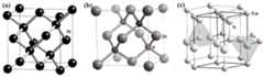
图1为三种半导体材料的晶体结构示意图;Figure 1 is a schematic diagram of the crystal structures of three semiconductor materials;
图2为三种半导体材料的晶格结构以及晶面示意图;Figure 2 is a schematic diagram of lattice structures and crystal planes of three semiconductor materials;
图3-图24为本申请实施例提供的一种半导体基底制作方法的工艺流程图。3-24 are process flow charts of a method for manufacturing a semiconductor substrate provided in an embodiment of the present application.
具体实施方式Detailed ways
下面将结合本申请实施例中的附图,对本申请中的实施例进行清楚、完整地描述,显然,所描述的实施例仅仅是本申请一部分实施例,而不是全部的实施例。基于本申请中的实施例,本领域普通技术人员在没有做出创造性劳动前提下所获得的所有其他实施例,都属于本申请保护的范围。The following will clearly and completely describe the embodiments of the present application with reference to the drawings in the embodiments of the present application. Obviously, the described embodiments are only some of the embodiments of the present application, not all of them. Based on the embodiments in this application, all other embodiments obtained by persons of ordinary skill in the art without making creative efforts belong to the scope of protection of this application.
常规技术中,一般III-V材料的基底一般采用InP。In conventional technologies, InP is generally used as a substrate of a general III-V material.
如图1所示,图1为三种半导体材料的晶体结构示意图,图1中(a)图为Si的晶格结构,图1中(b)图为InP的晶格结构,基于图1中(a)图和(b)图所示可知,InP为立方结构,与Si的晶格结构相同,用于SOI(绝缘体上硅)基底模板辅助横向异质外延不存在太大的障碍。图1中(c)图为GaN的晶格结构,并非是立方结构,无法直接基于SOI基底模板辅助横向异质外延形成。As shown in Figure 1, Figure 1 is a schematic diagram of the crystal structure of three semiconductor materials, (a) in Figure 1 shows the lattice structure of Si, and (b) in Figure 1 shows the lattice structure of InP, based on the As shown in (a) and (b), it can be seen that InP has a cubic structure, which is the same as the lattice structure of Si, and there is no big obstacle for SOI (silicon on insulator) substrate template-assisted lateral heteroepitaxy. (c) in Figure 1 shows the lattice structure of GaN, which is not a cubic structure, and cannot be formed directly based on SOI substrate template-assisted lateral heteroepitaxy.
由于GaN对Si的回熔刻蚀问题,需要在Si上外延层AlN,作为缓冲层与成核层,防止GaN与Si直接接触以及后续GaN的成核生长。但是AlN不能直接用模板辅助选择横向异质外延生长制备。Due to the remelting etching problem of GaN on Si, it is necessary to epitaxially layer AlN on Si as a buffer layer and nucleation layer to prevent direct contact between GaN and Si and the subsequent nucleation and growth of GaN. However, AlN cannot be directly prepared by template-assisted selective lateral heteroepitaxial growth.
如图2所示,图2为三种半导体材料的晶格结构以及晶面示意图,图2中(a)图为GaN的晶格结构及其(0001)晶面,图2中(b)图为Si的晶格结构及其(111)晶面,图2中(c)图为GaN晶格结构中(0001)晶面与Si晶格结构中(111)晶面的外延关系,图2中(d)图为GaN晶格结构中(0001)晶面与Si晶格结构中(111)晶面的晶向关系。As shown in Figure 2, Figure 2 is a schematic diagram of the lattice structure and crystal plane of three semiconductor materials, Figure 2 (a) shows the lattice structure of GaN and its (0001) crystal plane, Figure 2 (b) is the crystal lattice structure of Si and its (111) crystal plane, and (c) in Figure 2 shows the epitaxial relationship between the (0001) crystal plane in the GaN lattice structure and the (111) crystal plane in the Si lattice structure, in Figure 2 (d) The figure shows the crystal orientation relationship between the (0001) crystal plane in the GaN lattice structure and the (111) crystal plane in the Si lattice structure.
发明人研究发现,基于图2所示关系,可以利用SOI基底,通过两次刻蚀以及外延方式,形成高质量的GaN外延层。基于此制备的包括III-V材料GaN的半导体基底中,GaN层有一定的面积和较高的晶体质量,可以在其上外延和加工各种GaN分立器件,如微型电子器件和微型光电器件,可以用于通讯光电子、汽车光电子、光学传感等领域。The inventors found that, based on the relationship shown in FIG. 2 , an SOI substrate can be used to form a high-quality GaN epitaxial layer through two etchings and epitaxy. In the semiconductor substrate including III-V material GaN prepared based on this, the GaN layer has a certain area and high crystal quality, and various GaN discrete devices can be epitaxially and processed on it, such as microelectronic devices and micro optoelectronic devices, It can be used in communication optoelectronics, automotive optoelectronics, optical sensing and other fields.
有鉴于此,本申请技术方案提供了一种半导体基底、半导体器件以及制作方法,所述半导体基底的制作方法包括:In view of this, the technical solution of the present application provides a semiconductor substrate, a semiconductor device and a manufacturing method, and the manufacturing method of the semiconductor substrate includes:
提供一SOI基底,所述SOI基底包括:第一绝缘层;位于所述第一绝缘层上的至少一个单晶硅区块;第二绝缘层,所述第二绝缘层覆盖所述单晶硅区块以及所述单晶硅区块四周的所述第一绝缘层;在平行于所述SOI基底的方向上,所述单晶硅区块具有相对的第一端和第二端;An SOI substrate is provided, the SOI substrate includes: a first insulating layer; at least one monocrystalline silicon block located on the first insulating layer; a second insulating layer, the second insulating layer covers the monocrystalline silicon a block and the first insulating layer surrounding the single crystal silicon block; in a direction parallel to the SOI substrate, the single crystal silicon block has opposite first and second ends;
在所述第二绝缘层上形成第一窗口,露出所述单晶硅区块对应所述第一端的局部;forming a first window on the second insulating layer, exposing a part of the monocrystalline silicon block corresponding to the first end;
基于所述第一窗口露出的所述单晶硅区块,形成成核区块;forming a nucleation block based on the monocrystalline silicon block exposed by the first window;
形成贯穿所述第二绝缘层的第二窗口,露出所述单晶硅区块对应所述第二端的局部;forming a second window through the second insulating layer, exposing a portion of the monocrystalline silicon block corresponding to the second end;
基于所述第二窗口,去除所述单晶硅区块,形成位于所述第一绝缘层与所述第二绝缘层之间的间隙结构;Based on the second window, removing the monocrystalline silicon block to form a gap structure between the first insulating layer and the second insulating layer;
基于所述成核区块,在所述间隙结构内选择性横向外延生长GaN层。Based on the nucleation zone, a GaN layer is selectively laterally epitaxially grown within the interstitial structure.
本申请技术方案所述制作方法基于SOI基底,制备包括III-V材料GaN的半导体基底,能够降低GaN的晶格缺陷密度,进而能够提高基于半导体基底制备的半导体器件的性能。The manufacturing method described in the technical solution of the present application is based on an SOI substrate and prepares a semiconductor substrate including III-V material GaN, which can reduce the lattice defect density of GaN, thereby improving the performance of semiconductor devices prepared based on the semiconductor substrate.
可选的,所述制作方法可以通过选区外延方式形成成核层,再结合化学机械研磨(CMP)工艺,在所述第一窗口形成所述成核区块,无需模板辅助选择性横向异质外延制备AlN的缓冲层。Optionally, the manufacturing method may form a nucleation layer by selective epitaxy, combined with a chemical mechanical polishing (CMP) process, to form the nucleation block in the first window, without template-assisted selective lateral heterogeneity The buffer layer of AlN is prepared by epitaxy.
另外,所述制作方法基于SOI基底形成成核区块后,去除SOI基底中单晶硅区块后,基于去除单晶硅区块所形成的间隙结构形成GaN层,避免了GaN和Si的直接接触。In addition, the fabrication method forms a GaN layer based on the gap structure formed by removing the monocrystalline silicon block after removing the single crystal silicon block in the SOI substrate after forming a nucleation block based on the SOI substrate, thereby avoiding the direct interaction between GaN and Si. touch.
为使本申请的上述目的、特征和优点能够更加明显易懂,下面结合附图和具体实施方式对本申请作进一步详细的说明。In order to make the above objects, features and advantages of the present application more obvious and comprehensible, the present application will be further described in detail below in conjunction with the accompanying drawings and specific implementation methods.
参考图3-图24,图3-图24为本申请实施例提供的一种半导体基底制作方法的工艺流程图,该制作方法包括:Referring to FIG. 3-FIG. 24, FIG. 3-FIG. 24 is a process flow chart of a semiconductor substrate manufacturing method provided in an embodiment of the present application. The manufacturing method includes:
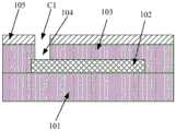
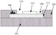
步骤S11:如图3和图4所示,提供一SOI基底100。Step S11 : as shown in FIG. 3 and FIG. 4 , an
所述SOI基底100包括:第一绝缘层101;位于所述第一绝缘层101上的至少一个单晶硅区块102;第二绝缘层103,所述第二绝缘层103覆盖所述单晶硅区块102以及所述单晶硅区块102四周的所述第一绝缘层101;在平行于所述SOI基底100的方向上,所述单晶硅区块102具有相对的第一端和第二端。在图4中,以左侧为第一端,右侧为第二端为例进行图示。The
其中,图3为SOI基底100的俯视图,图4为图3在A-A’方向的切面图。需要说明的是,SOI基底100中,单晶硅区块102的数量可以为一个或是多个,当具有多个单晶硅区块102时,单晶硅区块102的数量以及排布方式不局限于图3所示,还可以如图5所示,可以基于需求设置单晶硅区块102的数量以及排布方式,本申请实施例对此不作具体限定。Wherein, FIG. 3 is a top view of the
步骤S12:如图6-图9所示,在所述第二绝缘层103上形成第一窗口104,露出所述单晶硅区块102对应所述第一端的局部。Step S12: As shown in FIG. 6-FIG. 9, a
在该步骤中,基于光刻工艺形成所述第一窗口104。首先,如图6所示,在第二绝缘层103表面形成一层光刻胶105。然后,如图7所示,图形化光刻胶105,在光刻胶105对应第一窗口104的位置形成开口C1。再如图8所示,基于开口C1对第二绝缘层103进行刻蚀,在第二绝缘层103上形成第一窗口104。最后,如图9所示,去除第二绝缘层103表面的光刻胶105。In this step, the
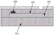
步骤S13:如图10-图12所示,基于所述第一窗口104露出的所述单晶硅区块102,形成成核区块106。Step S13 : as shown in FIGS. 10-12 , based on the
本申请实施例中,所述成核区块106为AlN区块,所述单晶硅区块102朝向所述第二绝缘层103的表面为单晶Si的(111)晶面。其中,AlN与GaN均为III-V材料,可以作为GaN的成核基材。而单晶Si的(111)晶面包括与GaN(0001)晶面适配的六边形,能够使得后续形成的GaN层111具有良好的晶格质量,降低其缺陷密度。如是,能够基于单晶Si的(111)晶面,直接通过表面外延生长形成AlN层,用于制备AlN区块,制作工艺简单,且能够基于单晶Si的(111)晶面,形成优质的AlN层,进而在后续工艺形成高质量的GaN层111。In the embodiment of the present application, the
在该步骤中,形成所述成核区块106的方法包括:In this step, the method for forming the
首先如图10所示,形成成核层107,所述成核层107至少填充部分所述第一窗口104,并覆盖所述第二绝缘层103背离所述第一绝缘层101的一侧表面。First, as shown in FIG. 10 , a
然后如图11所示,去除所述第二绝缘层103表面上的所述成核层107,保留所述第一窗口104内的所述成核层107,形成所述成核区块106。所述成核区块106与所述第二绝缘层103的表面齐平。可以通过CMP工艺将所述第二绝缘层103表面的成核层107去除,并去除部分所述第二绝缘层103,使得所述成核区块106与所述第二绝缘层103的表面齐平。Then, as shown in FIG. 11 , the
最后,如图12所示,在所述第二绝缘层103表面形成一层同材质的绝缘材料,形成新的第二绝缘层103。Finally, as shown in FIG. 12 , a layer of insulating material of the same material is formed on the surface of the second insulating
本申请实施例所述制作方法中,各个绝缘层均可以为氧化硅层。对应中材料的第一绝缘层101和第二绝缘层103二者相接触区域可以没有可见的分界面,图12中所示方式为了便于清楚图示相对层次结构,示出两者的界面区域。In the manufacturing method described in the embodiment of the present application, each insulating layer may be a silicon oxide layer. The contact area between the first insulating
步骤S14:如图13-图16所示,形成贯穿所述第二绝缘层103的第二窗口109,露出所述单晶硅区块102对应所述第二端的局部;Step S14: As shown in FIGS. 13-16 , forming a
该步骤中通过光刻工艺形成第二窗口109。与形成第一窗口104的方法相同,首先,如图13所示形成一层光刻胶,然后如图14所示,图形化光刻胶,在光刻胶对应第二窗口109的位置上形成开口,再如图15所示,基于光刻胶上的开口进行刻蚀,形成第二窗口109,最后如图16所示,去除光刻胶。In this step, the
第一窗口104在单晶硅区块102表面上的刻蚀深度可以为零或是大于零。第二窗口109在单晶硅区块102表面上的刻蚀深度大于零,从而对使得在形成第二窗口109时,对单晶硅区块102形成过刻蚀,提高第二窗口109所露出的单晶硅区块102的表面粗糙度,便于后续工艺去除单晶硅区块102时,对单晶硅区块102的刻蚀。The etching depth of the
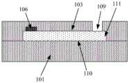
步骤S15:如图17所示,基于所述第二窗口109,去除所述单晶硅区块102,形成位于所述第一绝缘层101与所述第二绝缘层103之间的间隙结构110。Step S15: As shown in FIG. 17 , based on the
该步骤中,基于湿法刻蚀去除所述单晶硅区块102,基于上一步骤中第二窗口109对单晶硅区块102的过刻蚀,能够提高刻蚀过程中去除单晶硅区块102的速度。In this step, the
本申请实施例中,可以采用10%稀释的KOH溶液选择性刻蚀单晶硅区块102。在室温下,稀释的KOH溶液对AlN的刻蚀速率不高,可以基于刻蚀时间的控制,避免AlN区块完全刻蚀。In the embodiment of the present application, a 10% diluted KOH solution may be used to selectively etch the
需要说明的是,不局限于采用稀释的KOH溶液选择性刻蚀单晶硅区块102,也可以采用其他选择刻蚀比高的试剂刻蚀去除单晶硅区块102,本申请实施例对所采用的刻蚀试剂类型不限定。It should be noted that the selective etching of the
去除单晶硅区块102后,对基底进行清洗,以避免刻蚀残留物影响后续所制备GaN层111的晶格质量。After the single
步骤S16:如图18所示,基于所述成核区块106,在所述间隙结构110内选择性横向外延生长GaN层111。Step S16 : as shown in FIG. 18 , selectively laterally epitaxially grow a
可以采用MOCVD(金属有机化学气相沉积)工艺制备所述GaN层111。在MOCVD设备中,进行模板辅助选择性横向异质外延生长GaN。本申请技术方案中,基于单晶硅Si(111)晶面形成AlN成核区块,后续去除单晶硅区块102,基于SOI基底100的模板结构以及AlN成核区块,进行模板辅助选择性横向异质外延生长GaN,可以形成高质量的GaN层111,其缺陷密度小于103cm-2。The
如上述,本申请实施例所述制作方法中,形成所述第二窗口109的方法包括:基于光刻工艺,对所述第二绝缘层103进行刻蚀,形成所述第二窗口109;其中,过刻蚀所述第二绝缘层103,增大所述第二窗口109所露出的单晶硅区块102表面粗糙度,以便于后续工艺加快对单晶硅区块102的刻蚀速度。As mentioned above, in the manufacturing method described in the embodiment of the present application, the method for forming the
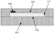
形成间隙结构110后,形成GaN层111之前的基底俯视图如图19所示,图19在A-A’方向的切面图如图17所示,图19在B-B’方向的切面图如图20所示。结合上述实施例附图以及图19和图20所示,所述单晶硅区块102为矩形;所述矩形相对的两侧边分别对应设置所述第一窗口104和所述第二窗口109,所述矩形相对的另外两侧边外侧的所述第二绝缘层103与所述第一绝缘层101接触,作为所述间隙结构110的支撑结构。具体的,如图20所示,在间隙结构110左右两侧的外侧,所述第二绝缘层103与所述第一绝缘层101接触,作为所述间隙结构110的支撑结构,能够避免形成间隙结构110后,第二绝缘层103由于重力产生裂纹或是坍塌。After the
基于多个单晶硅区块102能够形成多个器件结构,多个器件结构可以基于单晶硅区块102的布局阵列排布。基于单晶硅区块102的形状,可以形成对应形状的器件结构,本申请实施例对于单晶硅区块102的形状以及基于其形成的器件结构不作具体限定。在图19所示方式中,一个单晶硅区块102对应一个器件结构,器件结构在横向以及纵向上的尺寸可以为几微米到几十微米,可以基于需求调整。A plurality of device structures can be formed based on a plurality of single crystal silicon blocks 102 , and the plurality of device structures can be arranged in an array based on the layout of the single crystal silicon blocks 102 . Based on the shape of the
如上述,本申请实施例中,可以具有多个所述单晶硅区块102,相邻两个所述单晶硅区块102之间,所述第二绝缘层103与所述第一绝缘层101接触,以便于去除单晶硅区块102后,形成支撑结构。As mentioned above, in the embodiment of the present application, there may be multiple single crystal silicon blocks 102, between two adjacent single crystal silicon blocks 102, the second insulating
本申请实施例中,所述单晶硅区块102的厚度范围是100nm-900nm。在该厚度范围内,能够保证形成高质量的GaN层111。同时,在满足当前各种半导体器件所需的GaN层111厚度需求的同时,能够避免GaN层111厚度过大导致的器件体积增大。In the embodiment of the present application, the thickness range of the single
基于上述制作方法所制备的具有GaN层111的半导体基底可以作为用于制备GaN电子器件的平台,不局限于用于制备GaN的光电器件。The semiconductor substrate with the
基于单晶硅Si(111)晶面无法直接进行模板辅助横向外延AlN层,本申请技术方案采用两次刻蚀工艺分别形成第一窗口104和第二窗口109,基于第一窗口可以通过简单表面外延方式(第一次外延)在单晶硅Si(111)晶面形成AlN的成核区块106,基于第二窗口109去除单晶硅区块102,进而能够基于去除单晶硅区块102后所形成的间隙结构110以及AlN的成核区块106,外延形成GaN层111(第二次外延)。故本申请技术方案考虑到Si(111)面上模板辅助横向外延AlN的困难,采用两次刻蚀加两次外延工艺,可以形成高质量的AlN材质的成核区块106以及GaN层111。Since the single crystal silicon Si(111) crystal plane cannot directly carry out the template-assisted lateral epitaxy of the AlN layer, the technical solution of the present application adopts two etching processes to form the
基于上述实施例,本申请另一实施例还提供了一种半导体器件的制作方法,所述制作方法包括:Based on the above-mentioned embodiments, another embodiment of the present application also provides a manufacturing method of a semiconductor device, the manufacturing method comprising:
首先,提供上述实施例所述制作方法制备的半导体基底。Firstly, the semiconductor substrate prepared by the manufacturing method described in the above-mentioned embodiments is provided.
然后,基于半导体基底中GaN层111形成半导体器件的功能结构。Then, the functional structure of the semiconductor device is formed based on the
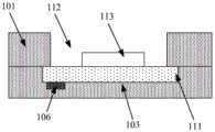
一种方式中,基于半导体基底中GaN层111形成半导体器件的功能结构,包括:如图21所示,在所述半导体基底上形成第三窗口112,露出至少部分所述GaN层111;再如图22所示,基于所述第三窗口112,在所述GaN层111表面上形成所述半导体器件的功能结构113。In one manner, forming the functional structure of the semiconductor device based on the
在图21和图22所示方式中,形成所述第三窗口112的方法包括:在朝向所述半导体基底的第二绝缘层103的一侧形成所述第三窗口112,所述第三窗口112位于所述半导体基底的成核区块106朝向所述半导体基底的第二窗口109的一侧,且与所述第二窗口109连通。该方式可以通过干法刻蚀去除GaN层111表面上的绝缘层,形成所述第三窗口112。In the manner shown in FIG. 21 and FIG. 22 , the method for forming the
其他方式中,形成所述第三窗口112的方法包括:如图23所示,在所述半导体基底的第二窗口109填充绝缘介质,并对所述半导体基底的第二绝缘层103背离所述半导体基底的第一绝缘层的一侧进行平坦化处理,可以通过CMP工艺进行平坦化处理;再如图24所示,在所述第一绝缘层101形成所述第三窗口112,以便于形成功能结构113。该方式中,同样可以通过干法刻蚀形成第三窗口113。In other ways, the method for forming the
本申请实施例中,在所述GaN层111表面上形成所述半导体基底的功能结构113,包括:基于外延工艺,在所述GaN层111的表面上制备GaN-HEMT器件的功能结构、或激光器功能结构、或LED功能结构。GaN层111可以作为半导体基底N极性面的层结构。各个区域的GaN层111可以分别对应一个分离的器件。In the embodiment of the present application, forming the
基于上述实施例,本申请另一实施例还提供了一种上述制作方法制备的半导体基底,所述半导体基底的结构可以参考上述实施例附图所示,包括:GaN层111,所述GaN层111相对的两侧分别覆盖有一层绝缘层(即第一绝缘层101和第二绝缘层102)。Based on the above embodiments, another embodiment of the present application also provides a semiconductor substrate prepared by the above manufacturing method. The structure of the semiconductor substrate can refer to the drawings of the above embodiments, including:
该实施例所述半导体基底为基于上述实施例所述制作方法制备,能够大大降低GaN层111中缺陷密度,提高半导体器件的性能。The semiconductor substrate described in this embodiment is prepared based on the manufacturing method described in the above embodiments, which can greatly reduce the defect density in the
基于上述实施例,本申请另一实施例还提供了一种半导体器件,所述半导体器件的结构如图22或是图24所示,包括:Based on the above embodiments, another embodiment of the present application also provides a semiconductor device, the structure of which is shown in Figure 22 or Figure 24, including:
上述制作方法制备的半导体基底,所述半导体基底的结构可以参考上述实施例附图所示,所述半导体基底具有GaN层111,所述GaN层111相对的两侧分别覆盖有一层绝缘层;For the semiconductor substrate prepared by the above manufacturing method, the structure of the semiconductor substrate can be referred to as shown in the drawings of the above embodiments, the semiconductor substrate has a
其中一层所述绝缘层具有露出所述GaN层111的窗口(上述第三窗口112);One of the insulating layers has a window exposing the GaN layer 111 (the above-mentioned third window 112);
基于所述窗口,位于所述GaN层111表面上的功能结构113。Based on the window, a
其中,所述半导体器件可以为GaN-HEMT器件、或激光器、或LED。Wherein, the semiconductor device may be a GaN-HEMT device, or a laser, or an LED.
本申请实施例所述半导体器件采用基于上述实施例制作方法制备的半导体基底,GaN层111具有良好的晶格结构,缺陷密度小,半导体器件具有良好的可靠性。The semiconductor device described in the embodiment of the present application adopts the semiconductor substrate prepared based on the manufacturing method of the above embodiment, the
本说明书中各个实施例采用递进、或并列、或递进和并列结合的方式描述,每个实施例重点说明的都是与其他实施例的不同之处,各个实施例之间相同相似部分互相参见即可。对于实施例公开的半导体器件及其制作方法、以及半导体基底而言,由于其与实施例公开的半导体基底的制作方法相对应,所以描述的比较简单,相关之处参见半导体基底的制作方法相关部分说明即可。Each embodiment in this specification is described in a progressive, parallel, or progressive and parallel manner. Each embodiment focuses on the differences from other embodiments. The same and similar parts between the various embodiments Just see it. For the semiconductor device disclosed in the embodiment, its manufacturing method, and the semiconductor substrate, since it corresponds to the manufacturing method of the semiconductor substrate disclosed in the embodiment, the description is relatively simple. For related information, please refer to the relevant part of the manufacturing method of the semiconductor substrate Just explain.
需要说明的是,在本申请的描述中,需要理解的是,幅图和实施例的描述是说明性的而不是限制性的。贯穿说明书实施例的同样的幅图标记标识同样的结构。另外,处于理解和易于描述,幅图可能夸大了一些层、膜、面板、区域等厚度。同时可以理解的是,当诸如层、膜、区域或基板的元件被称作“在”另一元件“上”时,该元件可以直接在其他元件上或者可以存在中间元件。另外,“在…上”是指将元件定位在另一元件上或者另一元件下方,但是本质上不是指根据重力方向定位在另一元件的上侧上。It should be noted that in the description of the present application, it should be understood that the descriptions of the figures and embodiments are illustrative rather than restrictive. Like figure numbers identify like structures throughout the embodiments of the specification. In addition, the drawings may exaggerate the thickness of some layers, films, panels, regions, etc. for the sake of understanding and ease of description. Also, it will be understood that when an element such as a layer, film, region, or substrate is referred to as being “on” another element, it can be directly on the other element or intervening elements may be present. In addition, "on" means positioning an element on or under another element, but does not essentially mean positioning on an upper side of another element according to the direction of gravity.
术语“上”、“下”、“顶”、“底”、“内”、“外”等指示的方位或位置关系为基于附图所示的方位或位置关系,仅是为了便于描述本申请和简化描述,而不是指示或暗示所指的装置或元件必须具有特定的方位、以特定的方位构造和操作,因此不能理解为对本申请的限制。当一个组件被认为是“连接”另一个组件,它可以是直接连接到另一个组件或者可能同时存在居中设置的组件。The orientation or positional relationship indicated by the terms "upper", "lower", "top", "bottom", "inner", "outer", etc. are based on the orientation or positional relationship shown in the drawings, and are only for the convenience of describing the present application and simplified descriptions, rather than indicating or implying that the device or element referred to must have a specific orientation, be constructed and operate in a specific orientation, and thus should not be construed as limiting the application. When a component is said to be "connected" to another component, it may be directly connected to the other component or there may be a centered component at the same time.
还需要说明的是,在本文中,诸如第一和第二等之类的关系术语仅仅用来将一个实体或者操作与另一个实体或操作区分开来,而不一定要求或者暗示这些实体或操作之间存在任何这种实际的关系或者顺序。而且,术语“包括”、“包含”或者其任何其他变体意在涵盖非排他性的包含,从而使得包括一系列要素的物品或者设备不仅包括那些要素,而且还包括没有明确列出的其他要素,或者是还包括为这种物品或者设备所固有的要素。在没有更多限制的情况下,由语句“包括一个……”限定的要素,并不排除在包括上述要素的物品或者设备中还存在另外的相同要素。It should also be noted that in this article, relational terms such as first and second etc. are only used to distinguish one entity or operation from another entity or operation, and do not necessarily require or imply that these entities or operations Any such actual relationship or order exists between. Moreover, the term "comprises", "comprises" or any other variation thereof is intended to cover a non-exclusive inclusion such that an article or device comprising a set of elements includes not only those elements but also other elements not expressly listed, Or also include elements inherent in the article or device. Without further limitations, an element defined by the phrase "comprising a ..." does not exclude the presence of additional identical elements in an article or device comprising the aforementioned element.
对所公开的实施例的上述说明,使本领域专业技术人员能够实现或使用本申请。对这些实施例的多种修改对本领域的专业技术人员来说将是显而易见的,本文中所定义的一般原理可以在不脱离本申请的精神或范围的情况下,在其它实施例中实现。因此,本申请将不会被限制于本文所示的这些实施例,而是要符合与本文所公开的原理和新颖特点相一致的最宽的范围。The above description of the disclosed embodiments is provided to enable any person skilled in the art to make or use the present application. Various modifications to these embodiments will be readily apparent to those skilled in the art, and the general principles defined herein may be implemented in other embodiments without departing from the spirit or scope of the application. Therefore, the present application will not be limited to the embodiments shown herein, but is to be accorded the widest scope consistent with the principles and novel features disclosed herein.
Claims (13)
Priority Applications (1)
| Application Number | Priority Date | Filing Date | Title |
|---|---|---|---|
| CN202211425086.3ACN116190203A (en) | 2022-11-15 | 2022-11-15 | Semiconductor substrate, semiconductor device and manufacturing method |
Applications Claiming Priority (1)
| Application Number | Priority Date | Filing Date | Title |
|---|---|---|---|
| CN202211425086.3ACN116190203A (en) | 2022-11-15 | 2022-11-15 | Semiconductor substrate, semiconductor device and manufacturing method |
Publications (1)
| Publication Number | Publication Date |
|---|---|
| CN116190203Atrue CN116190203A (en) | 2023-05-30 |
Family
ID=86441077
Family Applications (1)
| Application Number | Title | Priority Date | Filing Date |
|---|---|---|---|
| CN202211425086.3APendingCN116190203A (en) | 2022-11-15 | 2022-11-15 | Semiconductor substrate, semiconductor device and manufacturing method |
Country Status (1)
| Country | Link |
|---|---|
| CN (1) | CN116190203A (en) |
Citations (6)
| Publication number | Priority date | Publication date | Assignee | Title |
|---|---|---|---|---|
| US20060267017A1 (en)* | 2005-05-24 | 2006-11-30 | Samsung Electronics Co., Ltd. | Semi-conductor-on-insulator structure, semiconductor devices using the same and method of manufacturing the same |
| CN110289206A (en)* | 2019-05-21 | 2019-09-27 | 财团法人交大思源基金会 | Semiconductor structure and manufacturing method of GaN heterogeneously integrated on silicon substrate |
| CN111682061A (en)* | 2020-05-18 | 2020-09-18 | 华为技术有限公司 | Nitride epitaxial wafer and its preparation method and semiconductor device |
| TWI735188B (en)* | 2020-02-26 | 2021-08-01 | 香港科技大學 | Method for growing iii-v compound semiconductors on silicon-on-insulators |
| CN114743876A (en)* | 2022-03-14 | 2022-07-12 | 绍兴中芯集成电路制造股份有限公司 | Preparation method of buffer layer of epitaxial structure and preparation method of gallium nitride epitaxial layer |
| CN114883192A (en)* | 2022-04-25 | 2022-08-09 | 浙江集迈科微电子有限公司 | Monolithic heterogeneous integrated structure of silicon and III-V group device on insulating substrate and preparation method |
- 2022
- 2022-11-15CNCN202211425086.3Apatent/CN116190203A/enactivePending
Patent Citations (7)
| Publication number | Priority date | Publication date | Assignee | Title |
|---|---|---|---|---|
| US20060267017A1 (en)* | 2005-05-24 | 2006-11-30 | Samsung Electronics Co., Ltd. | Semi-conductor-on-insulator structure, semiconductor devices using the same and method of manufacturing the same |
| CN110289206A (en)* | 2019-05-21 | 2019-09-27 | 财团法人交大思源基金会 | Semiconductor structure and manufacturing method of GaN heterogeneously integrated on silicon substrate |
| TWI735188B (en)* | 2020-02-26 | 2021-08-01 | 香港科技大學 | Method for growing iii-v compound semiconductors on silicon-on-insulators |
| US20210265162A1 (en)* | 2020-02-26 | 2021-08-26 | The Hong Kong University Of Science And Technology | Method for growing iii-v compound semiconductors on silicon-on-insulators |
| CN111682061A (en)* | 2020-05-18 | 2020-09-18 | 华为技术有限公司 | Nitride epitaxial wafer and its preparation method and semiconductor device |
| CN114743876A (en)* | 2022-03-14 | 2022-07-12 | 绍兴中芯集成电路制造股份有限公司 | Preparation method of buffer layer of epitaxial structure and preparation method of gallium nitride epitaxial layer |
| CN114883192A (en)* | 2022-04-25 | 2022-08-09 | 浙江集迈科微电子有限公司 | Monolithic heterogeneous integrated structure of silicon and III-V group device on insulating substrate and preparation method |
Similar Documents
| Publication | Publication Date | Title |
|---|---|---|
| US9711623B2 (en) | FinFETs with vertical Fins and methods for forming the same | |
| CN100444323C (en) | Forming Lattice Modulated Semiconductor Substrates | |
| US8058705B2 (en) | Composite material substrate | |
| US7354840B1 (en) | Method for opto-electronic integration on a SOI substrate | |
| TWI787859B (en) | Method and system for integration of elemental and compound semiconductors on a ceramic substrate | |
| CN102790054A (en) | Germanium and III-V mixed coplanar semi-conductor structure and preparation method thereof | |
| CN102790084A (en) | Germanium and III-V mixed coplanar silicon on insulator (SOI) semi-conductor structure and preparation method thereof | |
| CN105340074B (en) | SOI substrate preparation method and SOI substrate | |
| CN209880627U (en) | III-V/Si heterostructure based on wafer bonding technology | |
| US7749817B2 (en) | Single-crystal layer on a dielectric layer | |
| CN113314394B (en) | Semiconductor substrate and preparation method of semiconductor structure | |
| US20160211136A1 (en) | Methods and structures for forming microstrip transmission lines on thin silicon carbide on insulator (sicoi) wafers | |
| CN116190203A (en) | Semiconductor substrate, semiconductor device and manufacturing method | |
| CN101944538A (en) | Semiconductor structure and manufacture method thereof | |
| KR101867999B1 (en) | Method of forming III-V group material layer, semiconductor device comprising III-V group material layer and method of manufacturing the same | |
| TWI851601B (en) | Photonics optoelectrical system and method for fabricating same | |
| TW202324779A (en) | Photonic-electronic integrated circuit chip and manufacturing method thereof | |
| CN114864680A (en) | Shielded gate trench device and method of making the same | |
| WO2012071763A1 (en) | Substrate for integrated circuit and forming method thereof | |
| CN115498059A (en) | Photodetector and method of forming the same | |
| US20240072184A1 (en) | Photodetectors on fin structure | |
| JPH06215993A (en) | Composite semiconductor substrate and manufacture thereof | |
| CN116111456B (en) | Silicon optical device integrated with III-V laser and manufacturing method thereof | |
| CN103187248B (en) | The preparation method of a kind of crystallographic orientation germanium on insulator wafer and device | |
| CN118712885A (en) | A method for preparing silicon-based thin film crystal based on silicon wafer heteroepitaxial growth |
Legal Events
| Date | Code | Title | Description |
|---|---|---|---|
| PB01 | Publication | ||
| PB01 | Publication | ||
| SE01 | Entry into force of request for substantive examination | ||
| SE01 | Entry into force of request for substantive examination |