CN116182919A - Three-axis high-temperature vibration sensor based on optical fiber F-P cavity and its preparation method - Google Patents
Three-axis high-temperature vibration sensor based on optical fiber F-P cavity and its preparation methodDownload PDFInfo
- Publication number
- CN116182919A CN116182919ACN202310440018.2ACN202310440018ACN116182919ACN 116182919 ACN116182919 ACN 116182919ACN 202310440018 ACN202310440018 ACN 202310440018ACN 116182919 ACN116182919 ACN 116182919A
- Authority
- CN
- China
- Prior art keywords
- optical fiber
- vibration
- triaxial
- mass block
- cavity
- Prior art date
- Legal status (The legal status is an assumption and is not a legal conclusion. Google has not performed a legal analysis and makes no representation as to the accuracy of the status listed.)
- Granted
Links
- 239000013307optical fiberSubstances0.000titleclaimsabstractdescription51
- 238000002360preparation methodMethods0.000titleabstractdescription19
- XUIMIQQOPSSXEZ-UHFFFAOYSA-NSiliconChemical compound[Si]XUIMIQQOPSSXEZ-UHFFFAOYSA-N0.000claimsabstractdescription85
- 229910052710siliconInorganic materials0.000claimsabstractdescription82
- 239000010703siliconSubstances0.000claimsabstractdescription82
- 238000005259measurementMethods0.000claimsdescription34
- 239000000835fiberSubstances0.000claimsdescription33
- 238000005530etchingMethods0.000claimsdescription27
- 238000005192partitionMethods0.000claimsdescription26
- 238000005516engineering processMethods0.000claimsdescription15
- 239000000758substrateSubstances0.000claimsdescription13
- 238000000034methodMethods0.000claimsdescription9
- 230000008878couplingEffects0.000claimsdescription3
- 238000010168coupling processMethods0.000claimsdescription3
- 238000005859coupling reactionMethods0.000claimsdescription3
- 238000004519manufacturing processMethods0.000claimsdescription2
- HJELPJZFDFLHEY-UHFFFAOYSA-Nsilicide(1-)Chemical compound[Si-]HJELPJZFDFLHEY-UHFFFAOYSA-N0.000claims4
- 230000001939inductive effectEffects0.000claims2
- 238000001020plasma etchingMethods0.000claims2
- 235000012431wafersNutrition0.000abstractdescription26
- 229920002120photoresistant polymerPolymers0.000description17
- 238000010586diagramMethods0.000description14
- 238000009616inductively coupled plasmaMethods0.000description11
- 238000000206photolithographyMethods0.000description6
- 230000008859changeEffects0.000description4
- 230000003287optical effectEffects0.000description3
- 238000010438heat treatmentMethods0.000description2
- 230000006872improvementEffects0.000description2
- 238000000608laser ablationMethods0.000description2
- 238000004806packaging method and processMethods0.000description2
- 230000008569processEffects0.000description2
- PNEYBMLMFCGWSK-UHFFFAOYSA-NAluminaChemical compound[O-2].[O-2].[O-2].[Al+3].[Al+3]PNEYBMLMFCGWSK-UHFFFAOYSA-N0.000description1
- 230000001133accelerationEffects0.000description1
- 230000006978adaptationEffects0.000description1
- 230000009286beneficial effectEffects0.000description1
- 238000004364calculation methodMethods0.000description1
- 230000015556catabolic processEffects0.000description1
- 238000004140cleaningMethods0.000description1
- 230000001427coherent effectEffects0.000description1
- 238000006731degradation reactionMethods0.000description1
- 239000000463materialSubstances0.000description1
- SBEQWOXEGHQIMW-UHFFFAOYSA-NsiliconChemical compound[Si].[Si]SBEQWOXEGHQIMW-UHFFFAOYSA-N0.000description1
- 239000002210silicon-based materialSubstances0.000description1
- 125000006850spacer groupChemical group0.000description1
- 230000003595spectral effectEffects0.000description1
Images


Classifications
- G—PHYSICS
- G01—MEASURING; TESTING
- G01D—MEASURING NOT SPECIALLY ADAPTED FOR A SPECIFIC VARIABLE; ARRANGEMENTS FOR MEASURING TWO OR MORE VARIABLES NOT COVERED IN A SINGLE OTHER SUBCLASS; TARIFF METERING APPARATUS; MEASURING OR TESTING NOT OTHERWISE PROVIDED FOR
- G01D5/00—Mechanical means for transferring the output of a sensing member; Means for converting the output of a sensing member to another variable where the form or nature of the sensing member does not constrain the means for converting; Transducers not specially adapted for a specific variable
- G01D5/26—Mechanical means for transferring the output of a sensing member; Means for converting the output of a sensing member to another variable where the form or nature of the sensing member does not constrain the means for converting; Transducers not specially adapted for a specific variable characterised by optical transfer means, i.e. using infrared, visible, or ultraviolet light
- G01D5/32—Mechanical means for transferring the output of a sensing member; Means for converting the output of a sensing member to another variable where the form or nature of the sensing member does not constrain the means for converting; Transducers not specially adapted for a specific variable characterised by optical transfer means, i.e. using infrared, visible, or ultraviolet light with attenuation or whole or partial obturation of beams of light
- G01D5/34—Mechanical means for transferring the output of a sensing member; Means for converting the output of a sensing member to another variable where the form or nature of the sensing member does not constrain the means for converting; Transducers not specially adapted for a specific variable characterised by optical transfer means, i.e. using infrared, visible, or ultraviolet light with attenuation or whole or partial obturation of beams of light the beams of light being detected by photocells
- G01D5/353—Mechanical means for transferring the output of a sensing member; Means for converting the output of a sensing member to another variable where the form or nature of the sensing member does not constrain the means for converting; Transducers not specially adapted for a specific variable characterised by optical transfer means, i.e. using infrared, visible, or ultraviolet light with attenuation or whole or partial obturation of beams of light the beams of light being detected by photocells influencing the transmission properties of an optical fibre
- G01D5/35306—Mechanical means for transferring the output of a sensing member; Means for converting the output of a sensing member to another variable where the form or nature of the sensing member does not constrain the means for converting; Transducers not specially adapted for a specific variable characterised by optical transfer means, i.e. using infrared, visible, or ultraviolet light with attenuation or whole or partial obturation of beams of light the beams of light being detected by photocells influencing the transmission properties of an optical fibre using an interferometer arrangement
- G01D5/35309—Mechanical means for transferring the output of a sensing member; Means for converting the output of a sensing member to another variable where the form or nature of the sensing member does not constrain the means for converting; Transducers not specially adapted for a specific variable characterised by optical transfer means, i.e. using infrared, visible, or ultraviolet light with attenuation or whole or partial obturation of beams of light the beams of light being detected by photocells influencing the transmission properties of an optical fibre using an interferometer arrangement using multiple waves interferometer
- G01D5/35312—Mechanical means for transferring the output of a sensing member; Means for converting the output of a sensing member to another variable where the form or nature of the sensing member does not constrain the means for converting; Transducers not specially adapted for a specific variable characterised by optical transfer means, i.e. using infrared, visible, or ultraviolet light with attenuation or whole or partial obturation of beams of light the beams of light being detected by photocells influencing the transmission properties of an optical fibre using an interferometer arrangement using multiple waves interferometer using a Fabry Perot
- B—PERFORMING OPERATIONS; TRANSPORTING
- B81—MICROSTRUCTURAL TECHNOLOGY
- B81B—MICROSTRUCTURAL DEVICES OR SYSTEMS, e.g. MICROMECHANICAL DEVICES
- B81B3/00—Devices comprising flexible or deformable elements, e.g. comprising elastic tongues or membranes
- B81B3/0018—Structures acting upon the moving or flexible element for transforming energy into mechanical movement or vice versa, i.e. actuators, sensors, generators
- B81B3/0021—Transducers for transforming electrical into mechanical energy or vice versa
- B—PERFORMING OPERATIONS; TRANSPORTING
- B81—MICROSTRUCTURAL TECHNOLOGY
- B81C—PROCESSES OR APPARATUS SPECIALLY ADAPTED FOR THE MANUFACTURE OR TREATMENT OF MICROSTRUCTURAL DEVICES OR SYSTEMS
- B81C1/00—Manufacture or treatment of devices or systems in or on a substrate
- B81C1/00015—Manufacture or treatment of devices or systems in or on a substrate for manufacturing microsystems
- B81C1/00134—Manufacture or treatment of devices or systems in or on a substrate for manufacturing microsystems comprising flexible or deformable structures
- B81C1/0015—Cantilevers
- C—CHEMISTRY; METALLURGY
- C30—CRYSTAL GROWTH
- C30B—SINGLE-CRYSTAL GROWTH; UNIDIRECTIONAL SOLIDIFICATION OF EUTECTIC MATERIAL OR UNIDIRECTIONAL DEMIXING OF EUTECTOID MATERIAL; REFINING BY ZONE-MELTING OF MATERIAL; PRODUCTION OF A HOMOGENEOUS POLYCRYSTALLINE MATERIAL WITH DEFINED STRUCTURE; SINGLE CRYSTALS OR HOMOGENEOUS POLYCRYSTALLINE MATERIAL WITH DEFINED STRUCTURE; AFTER-TREATMENT OF SINGLE CRYSTALS OR A HOMOGENEOUS POLYCRYSTALLINE MATERIAL WITH DEFINED STRUCTURE; APPARATUS THEREFOR
- C30B33/00—After-treatment of single crystals or homogeneous polycrystalline material with defined structure
- C30B33/08—Etching
- C30B33/12—Etching in gas atmosphere or plasma
- G—PHYSICS
- G01—MEASURING; TESTING
- G01D—MEASURING NOT SPECIALLY ADAPTED FOR A SPECIFIC VARIABLE; ARRANGEMENTS FOR MEASURING TWO OR MORE VARIABLES NOT COVERED IN A SINGLE OTHER SUBCLASS; TARIFF METERING APPARATUS; MEASURING OR TESTING NOT OTHERWISE PROVIDED FOR
- G01D11/00—Component parts of measuring arrangements not specially adapted for a specific variable
- G01D11/24—Housings ; Casings for instruments
- G01D11/245—Housings for sensors
- G—PHYSICS
- G01—MEASURING; TESTING
- G01H—MEASUREMENT OF MECHANICAL VIBRATIONS OR ULTRASONIC, SONIC OR INFRASONIC WAVES
- G01H9/00—Measuring mechanical vibrations or ultrasonic, sonic or infrasonic waves by using radiation-sensitive means, e.g. optical means
- G01H9/004—Measuring mechanical vibrations or ultrasonic, sonic or infrasonic waves by using radiation-sensitive means, e.g. optical means using fibre optic sensors
- B—PERFORMING OPERATIONS; TRANSPORTING
- B81—MICROSTRUCTURAL TECHNOLOGY
- B81B—MICROSTRUCTURAL DEVICES OR SYSTEMS, e.g. MICROMECHANICAL DEVICES
- B81B2201/00—Specific applications of microelectromechanical systems
- B81B2201/02—Sensors
- B81B2201/0285—Vibration sensors
- Y—GENERAL TAGGING OF NEW TECHNOLOGICAL DEVELOPMENTS; GENERAL TAGGING OF CROSS-SECTIONAL TECHNOLOGIES SPANNING OVER SEVERAL SECTIONS OF THE IPC; TECHNICAL SUBJECTS COVERED BY FORMER USPC CROSS-REFERENCE ART COLLECTIONS [XRACs] AND DIGESTS
- Y02—TECHNOLOGIES OR APPLICATIONS FOR MITIGATION OR ADAPTATION AGAINST CLIMATE CHANGE
- Y02T—CLIMATE CHANGE MITIGATION TECHNOLOGIES RELATED TO TRANSPORTATION
- Y02T90/00—Enabling technologies or technologies with a potential or indirect contribution to GHG emissions mitigation
Landscapes
- Engineering & Computer Science (AREA)
- Physics & Mathematics (AREA)
- General Physics & Mathematics (AREA)
- Chemical & Material Sciences (AREA)
- Manufacturing & Machinery (AREA)
- Microelectronics & Electronic Packaging (AREA)
- Materials Engineering (AREA)
- Metallurgy (AREA)
- Organic Chemistry (AREA)
- Analytical Chemistry (AREA)
- Computer Hardware Design (AREA)
- Crystallography & Structural Chemistry (AREA)
- Plasma & Fusion (AREA)
- Measurement Of Mechanical Vibrations Or Ultrasonic Waves (AREA)
Abstract
Description
Translated fromChinese技术领域technical field
本发明涉及微机电系统技术领域,尤其涉及基于光纤F-P腔的三轴高温振动传感器及其制备方法。The invention relates to the technical field of micro-electromechanical systems, in particular to a three-axis high-temperature vibration sensor based on an optical fiber F-P cavity and a preparation method thereof.
背景技术Background technique
基于微机电系统(MEMS)技术的高温振动传感器在航空发动机振动信号的测量中起着极其重要的作用。由于航空发动机的振动为多轴向耦合振动,这就需要传感器能同时测量三个轴向的振动信号,且能在航空发动机的高温环境下正常工作。High-temperature vibration sensors based on microelectromechanical systems (MEMS) technology play an extremely important role in the measurement of vibration signals of aeroengines. Since the vibration of the aero-engine is multi-axial coupling vibration, it is required that the sensor can measure the vibration signals of three axes at the same time, and can work normally in the high-temperature environment of the aero-engine.
目前,对MEMS高温振动传感器的研究主要包括压电式、压阻式和光纤式,且主要是针对单个轴向振动的测量。公开号为CN215524821U的实用新型专利中提出了一种新型高温三轴向压电式振动传感器,该传感器采用压电式原理,在高温环境下存在压电性能退化问题,影响传感器在高温环境下的实际测量精度,且其实际使用温度上限为500°C;公开号为CN113624328A的发明专利申请文件中提出了一种微型耐高温光纤法珀振动传感器,该传感器能在700°C的高温环境下工作,具有很强的抗干扰性,但其只能测量单个轴向的振动信号。目前现有技术还远不能满足对航空发动机内部振动测量所需的耐高温和三轴向测量的要求。At present, research on MEMS high-temperature vibration sensors mainly includes piezoelectric, piezoresistive and optical fiber types, and is mainly aimed at the measurement of a single axial vibration. A utility model patent with the publication number CN215524821U proposes a new type of high-temperature triaxial piezoelectric vibration sensor. The sensor adopts the piezoelectric principle, and there is a problem of piezoelectric performance degradation in high-temperature environments, which affects the performance of the sensor in high-temperature environments. The actual measurement accuracy, and the upper limit of the actual use temperature is 500°C; the invention patent application document with the publication number CN113624328A proposes a miniature high-temperature-resistant fiber-optic vibration sensor, which can work in a high-temperature environment of 700°C , has strong anti-interference, but it can only measure the vibration signal of a single axis. At present, the existing technology is still far from meeting the requirements of high temperature resistance and triaxial measurement required for internal vibration measurement of aero-engines.
发明内容Contents of the invention
针对上述存在的问题,本发明旨在提供基于光纤F-P腔的三轴高温振动传感器及其制备方法,能够满足对航空发动机内部振动测量所需的耐高温和三轴向测量的要求。In view of the above existing problems, the present invention aims to provide a triaxial high-temperature vibration sensor based on an optical fiber F-P cavity and its preparation method, which can meet the requirements of high temperature resistance and triaxial measurement required for internal vibration measurement of aeroengines.
为了实现上述目的,本发明所采用的技术方案如下:In order to achieve the above object, the technical scheme adopted in the present invention is as follows:
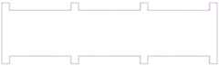
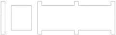
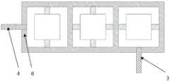
基于光纤F-P腔的三轴高温振动传感器,其特征在于:包括顶层硅和基底硅,所述顶层硅和基底硅之间设有三轴振动敏感结构,所述三轴振动敏感结构的前侧和左侧分别对应设有x轴测量光纤和y轴测量光纤,所述基底硅上设有z轴测量光纤。The triaxial high-temperature vibration sensor based on the optical fiber F-P cavity is characterized in that: it includes a top layer of silicon and a base silicon, a triaxial vibration sensitive structure is arranged between the top layer of silicon and the base silicon, and the front side and left side of the triaxial vibration sensitive structure An x-axis measuring fiber and a y-axis measuring fiber are correspondingly arranged on the sides, and a z-axis measuring fiber is arranged on the silicon substrate.
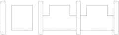
进一步的,所述三轴振动敏感结构包括外壳体,所述外壳体内设有两个隔板,两个所述隔板将所述外壳体分隔成三个腔室,三个腔室内从左往后依次对应设有第一质量块、第二质量块和第三质量块,所述第一质量块的前侧和后侧与外壳体之间设有第一固支梁;所述第二质量块的前侧和后侧与外壳体之间,以及第二质量块的左侧和右侧与两个隔板之间均设有第二固支梁,所述第三质量块的左侧和右侧与相互对应的隔板和外壳体之间均设有第三固支梁。Further, the three-axis vibration-sensitive structure includes an outer casing, and two partitions are arranged in the outer casing, and the two partitions divide the outer casing into three chambers, and the three chambers are arranged from left to right. Afterwards, a first mass block, a second mass block and a third mass block are correspondingly arranged in turn, and a first fixed support beam is provided between the front side and the rear side of the first mass block and the outer casing; the second mass block A second fixed support beam is provided between the front side and the rear side of the block and the outer shell, and between the left side and the right side of the second mass block and the two partitions, and the left side and the right side of the third mass block A third fixed support beam is arranged between the right side and the corresponding partition board and the outer casing.
进一步的,所述x轴测量光纤位于所述外壳体的前侧壁上,且所述x轴测量光纤的中心与所述第三质量块的中心位于同一水平线上;所述y轴测量光纤位于所述外壳体的左侧壁上,且所述y轴测量光纤的中心与所述第一质量块的中心位于同一水平线上;所述z轴测量光纤的中心与所述第二质量块的中心位于同一竖直线上。Further, the x-axis measurement optical fiber is located on the front side wall of the outer casing, and the center of the x-axis measurement optical fiber is on the same horizontal line as the center of the third proof mass; the y-axis measurement optical fiber is located on the On the left side wall of the outer casing, and the center of the y-axis measuring fiber is on the same level as the center of the first mass; the center of the z-axis measuring fiber is at the same level as the center of the second mass on the same vertical line.
进一步的,所述第三质量块与所述外壳体和相邻的隔板之间围成的空腔形成x轴测量振动F-P腔;所述第一质量块与所述外壳体和相邻的隔板之间围成的空腔形成y轴测量振动F-P腔;所述第二质量块与所述外壳体和两个隔板之间围成的空腔形成z轴测量振动F-P腔。Further, the cavity enclosed between the third mass block and the outer casing and adjacent partitions forms an x-axis measurement vibration F-P cavity; the first mass block and the outer casing and adjacent partitions The cavity enclosed between the partitions forms a y-axis measurement vibration F-P cavity; the cavity enclosed between the second mass block, the outer shell and the two partitions forms a z-axis measurement vibration F-P cavity.
进一步的,所述外壳体的厚度为1000μm,所述顶层硅和基底硅的厚度均为500μm。Further, the thickness of the outer casing is 1000 μm, and the thicknesses of the top silicon layer and the base silicon layer are both 500 μm.
进一步的,所述x轴测量光纤和y轴测量光纤的直径为600μm,所述z轴测量光纤的直径为1.8mm。Further, the diameters of the x-axis measuring fiber and the y-axis measuring fiber are 600 μm, and the diameter of the z-axis measuring fiber is 1.8 mm.
进一步的,基于光纤F-P腔的三轴高温振动传感器的制备方法,其特征在于,包括以下步骤,Further, the preparation method of the triaxial high-temperature vibration sensor based on the optical fiber F-P cavity is characterized in that it comprises the following steps,
S1:对顶层硅、基底硅和用于制备三轴振动敏感结构的硅晶片进行预处理;S1: Pretreatment of top silicon, base silicon, and silicon wafers for fabrication of triaxial vibration-sensitive structures;
S2:采用电感耦合等离子体刻蚀技术,对用于制备三轴振动敏感结构的硅晶片进行刻蚀,制备三轴振动敏感结构;S2: Using inductively coupled plasma etching technology to etch the silicon wafer used to prepare the triaxial vibration sensitive structure to prepare the triaxial vibration sensitive structure;
S3:采用电感耦合等离子体刻蚀技术刻蚀基底硅,形成通孔结构;S3: using inductively coupled plasma etching technology to etch the substrate silicon to form a through-hole structure;
S4:将刻蚀好的三轴振动敏感结构与顶层硅和基底硅在键合机中抽真空进行高温键合;S4: Vacuumize the etched triaxial vibration-sensitive structure with the top silicon and base silicon in a bonding machine for high-temperature bonding;
S5:采用飞秒激光烧蚀三轴振动敏感结构的前侧壁和左侧壁形成通孔结构,并在基底硅、三轴振动敏感结构前侧壁和左侧壁上的通孔结构处对应粘接x轴测量光纤、y轴测量光纤和z轴测量光纤。S5: Use femtosecond laser ablation of the front side wall and left side wall of the triaxial vibration sensitive structure to form a through hole structure, and correspond to the through hole structure on the substrate silicon, the front side wall and the left side wall of the triaxial vibration sensitive structure Bond the x-axis measurement fiber, y-axis measurement fiber and z-axis measurement fiber.
本发明的有益效果是:与现有技术相比,本发明的改进之处在于,The beneficial effect of the present invention is: compared with prior art, the improvement of the present invention is that,
1、本发明中提出的基于光纤F-P腔的三轴高温振动传感器,将三个固支梁-质量块系统集成在一个外壳体(一个芯片)上,构成三轴振动敏感结构,每个固支梁-质量块系统都呈中心对称,通过在不同的轴向插入测量光纤,可以同时测量同一点处三个不同轴向的振动信号。1. The three-axis high-temperature vibration sensor based on the optical fiber F-P cavity proposed in the present invention integrates three fixed-supported beam-mass systems on one outer shell (one chip) to form a three-axis vibration-sensitive structure. Each fixed-supported The beam-mass system is symmetrical to the center, and by inserting measuring optical fibers in different axes, the vibration signals of three different axes at the same point can be measured simultaneously.
2、本发明中提出的基于光纤F-P腔的三轴高温振动传感器,在一个芯片上一体化三轴向振动传感器,减小了传感器的封装体积,提高了整体的结构强度,且封装后一体化的三轴振动传感器对被测物体的原本状态影响较小。2. The triaxial high-temperature vibration sensor based on the optical fiber F-P cavity proposed in the present invention integrates the triaxial vibration sensor on one chip, reduces the packaging volume of the sensor, improves the overall structural strength, and integrates after packaging The three-axis vibration sensor has little influence on the original state of the measured object.
3、本发明中提出的基于光纤F-P腔的三轴高温振动传感器,采用三层硅片高温直接键合,避免了不同材料热膨胀系数的差异在高温下引起的热适配问题,利用了硅材料本身在高温环境下具有优秀的机械性能、高稳定性等优点,可实现传感器在800°C环境温度下工作。3. The three-axis high-temperature vibration sensor based on the optical fiber F-P cavity proposed in the present invention adopts three-layer silicon wafer high-temperature direct bonding, which avoids the thermal adaptation problem caused by the difference in thermal expansion coefficient of different materials at high temperature, and uses silicon material It has the advantages of excellent mechanical properties and high stability in high temperature environment, and can realize the sensor working at an ambient temperature of 800°C.
附图说明Description of drawings
图1为本发明三轴高温振动传感器的结构俯视图。Fig. 1 is a top view of the structure of the three-axis high-temperature vibration sensor of the present invention.
图2为本发明三轴高温振动传感器的结构主视图。Fig. 2 is a front view of the structure of the three-axis high-temperature vibration sensor of the present invention.
图3为本发明实施例二的三轴高温振动传感器制备过程中步骤S201示意图。FIG. 3 is a schematic diagram of step S201 in the preparation process of the triaxial high-temperature vibration sensor according to the second embodiment of the present invention.
图4为本发明实施例二的三轴高温振动传感器制备过程中步骤S202示意图。FIG. 4 is a schematic diagram of step S202 in the preparation process of the triaxial high-temperature vibration sensor according to the second embodiment of the present invention.
图5为本发明实施例二的三轴高温振动传感器制备过程中步骤S203示意图。FIG. 5 is a schematic diagram of step S203 in the preparation process of the triaxial high-temperature vibration sensor according to the second embodiment of the present invention.
图6为本发明实施例二的三轴高温振动传感器制备过程中步骤S204示意图。FIG. 6 is a schematic diagram of step S204 in the preparation process of the triaxial high-temperature vibration sensor according to the second embodiment of the present invention.
图7为本发明实施例二的三轴高温振动传感器制备过程中步骤S205示意图。FIG. 7 is a schematic diagram of step S205 in the preparation process of the triaxial high-temperature vibration sensor according to the second embodiment of the present invention.
图8为本发明实施例二的三轴高温振动传感器制备过程中步骤S206示意图。FIG. 8 is a schematic diagram of step S206 in the preparation process of the triaxial high-temperature vibration sensor according to the second embodiment of the present invention.
图9为本发明实施例二的三轴高温振动传感器制备过程中步骤S207示意图。FIG. 9 is a schematic diagram of step S207 in the preparation process of the triaxial high-temperature vibration sensor according to the second embodiment of the present invention.
图10为本发明实施例二的三轴高温振动传感器制备过程中步骤S208示意图。FIG. 10 is a schematic diagram of step S208 in the preparation process of the triaxial high-temperature vibration sensor according to the second embodiment of the present invention.
图11为本发明实施例二的三轴高温振动传感器制备过程中步骤S209示意图。FIG. 11 is a schematic diagram of step S209 in the preparation process of the triaxial high-temperature vibration sensor according to the second embodiment of the present invention.
图12为本发明实施例二的三轴高温振动传感器制备过程中步骤S210示意图。FIG. 12 is a schematic diagram of step S210 in the preparation process of the triaxial high-temperature vibration sensor according to the second embodiment of the present invention.
图13为本发明实施例二的三轴高温振动传感器制备过程中步骤S301示意图。FIG. 13 is a schematic diagram of step S301 in the preparation process of the triaxial high-temperature vibration sensor according to the second embodiment of the present invention.
图14为本发明实施例二的三轴高温振动传感器制备过程中步骤S302示意图。FIG. 14 is a schematic diagram of step S302 in the preparation process of the triaxial high-temperature vibration sensor according to the second embodiment of the present invention.
图15为本发明实施例二的三轴高温振动传感器制备过程中步骤S4示意图。FIG. 15 is a schematic diagram of step S4 in the preparation process of the triaxial high-temperature vibration sensor according to the second embodiment of the present invention.
图16为本发明实施例二的三轴高温振动传感器制备过程中步骤S5示意图。FIG. 16 is a schematic diagram of step S5 in the preparation process of the triaxial high-temperature vibration sensor according to the second embodiment of the present invention.
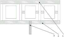
其中:1-顶层硅,2-基底硅,3-x轴测量光纤,4-y轴测量光纤,5-z轴测量光纤,6-外壳体,7-隔板,8-第一质量块,9-第二质量块,10-第三质量块,11-第一固支梁,12-第二固支梁,13-第三固支梁,14-x轴测量振动F-P腔,15-y轴测量振动F-P腔,16-z轴测量振动F-P腔。Among them: 1-top silicon, 2-base silicon, 3-x-axis measurement fiber, 4-y-axis measurement fiber, 5-z-axis measurement fiber, 6-outer shell, 7-partition, 8-first mass block, 9-the second mass, 10-the third mass, 11-the first fixed beam, 12-the second fixed beam, 13-the third fixed beam, 14-x-axis vibration F-P cavity, 15-y The axis measures the vibrating F-P cavity, and the 16-z axis measures the vibrating F-P cavity.
具体实施方式Detailed ways
为了使本领域的普通技术人员能更好的理解本发明的技术方案,下面结合附图和实施例对本发明的技术方案做进一步的描述。In order to enable those skilled in the art to better understand the technical solution of the present invention, the technical solution of the present invention will be further described below in conjunction with the accompanying drawings and embodiments.
实施例1Example 1
参照附图1-2所示的基于光纤F-P腔的三轴高温振动传感器,包括顶层硅1和基底硅2,所述顶层硅1和基底硅2之间设有三轴振动敏感结构,所述三轴振动敏感结构的前侧和左侧分别对应设有x轴测量光纤3和y轴测量光纤4,所述基底硅2上设有z轴测量光纤5;顶层硅1、基底硅2和三轴振动敏感结构均采用硅晶片材质,顶层硅1和基底硅2采用硅硅高温直接键合在三轴振动敏感结构两侧,键合条件包括底板温度360℃,键合腔室真空度1.0×10⁻⁴Pa,压力头压力25000N,键合时间2h45min。Referring to the three-axis high-temperature vibration sensor based on the optical fiber FP cavity shown in accompanying drawings 1-2, it includes a
具体的,所述三轴振动敏感结构包括外壳体6,所述外壳体6为一个硅晶片结构,所述外壳体6内设有两个隔板7,两个所述隔板7将所述外壳体分隔成三个大小相同且左右对称的腔室(采用电感耦合等离子体刻蚀技术对外壳体6进行干法刻蚀,形成具有两个隔板7三个腔室的结构),三个腔室内从左往后依次对应设有第一质量块8、第二质量块9和第三质量块10,所述第一质量块8、第二质量块9和第三质量块10的中心均与对应的腔室中心重合;所述第一质量块8的前侧和后侧与外壳体6之间设有第一固支梁11,第一质量块8通过第一固支梁11与外壳体6的前侧壁和后侧壁固定连接;所述第二质量块9的前侧和后侧与外壳体6之间,以及第二质量块9的左侧和右侧与两个隔板7之间均设有第二固支梁12,第二质量块9通过第二固支梁12与外壳体6的前侧壁、后侧壁和两个隔板7固定连接;所述第三质量块10的左侧和右侧与相互对应的隔板7和外壳体6之间均设有第三固支梁13,第三质量块10通过第三固支梁13与外壳体6的右侧壁以及相邻的隔板7固定连接。Specifically, the three-axis vibration-sensitive structure includes an
所述x轴测量光纤3位于所述外壳体6的前侧壁上,所述外壳体6的前侧壁上开设有通孔,x轴测量光纤3通过外壳体6前侧壁上的通孔粘接固定在外壳体6上,且所述x轴测量光纤3与外壳体6的前侧壁垂直设置,中心与所述第三质量块10的中心位于同一水平线上;所述y轴测量光纤4位于所述外壳体6的左侧壁上,所述外壳体6的左侧壁上开设有通孔,y轴测量光纤4通过外壳体6左侧壁上的通孔粘接固定在外壳体6上,且所述y轴测量光纤4与外壳体6的左侧壁垂直设置,中心与所述第一质量块8的中心位于同一水平线上;所述基底硅2上开设有通孔,z轴测量光纤5通过基底硅2上的通孔与基底硅2粘接固定,所述z轴测量光纤5的中心与所述第二质量块9的中心位于同一竖直线上;x轴测量光纤3、y轴测量光纤4和z轴测量光纤5的延长线两两相互垂直。The x-axis measuring
进一步的,所述第三质量块10与所述外壳体6和相邻的隔板7之间围成的空腔形成x轴测量振动F-P腔14,用于测量x轴方向被测振动;所述第一质量块8与所述外壳体6和相邻的隔板7之间围成的空腔形成y轴测量振动F-P腔15,用于测量y轴方向被测振动;所述第二质量块9与所述外壳体6和两个隔板7之间围成的空腔形成z轴测量振动F-P腔16,用于测量z轴被测振动;x轴测量光纤3、y轴测量光纤4和z轴测量光纤5与相互对应的测量振动F-P腔相互配合,可以测量被测振动变化引起的光谱变化,即测量振动F-P腔腔长值的变化。Further, the cavity surrounded by the
优选的,所述外壳体6的厚度为1000μm,所述顶层硅1和基底硅2的厚度均为500μm。Preferably, the thickness of the
优选的,所述x轴测量光纤3和y轴测量光纤4的直径为600μm,所述z轴测量光纤5的直径为1.8mm。Preferably, the
本实施例中三轴高温振动传感器的工作原理为:光源发出的光经光学处理后形成平行光,再经分束器分成三束光,三束光分别经过x轴测量光纤3、y轴测量光纤4和z轴测量光纤5入射至对应的质量块上,在测量光纤的端面和对应的质量块表面上发生反射,反射回的两束相干光发生干涉,再经过光纤环形器传输到光路解调系统中。The working principle of the three-axis high-temperature vibration sensor in this embodiment is: the light emitted by the light source is optically processed to form parallel light, and then divided into three beams of light by a beam splitter, and the three beams of light are respectively passed through the
当外界发生振动,测量x轴方向振动时,第三固支梁13和第三质量块10构成的固支梁-质量块振动敏感结构发生振动,导致测量振动的x轴测量振动F-P腔14的腔长值发生变化,在x轴测量光纤3的上端面和第三质量块10的下表面上反射回的两束光的光程差发生变化,通过解调光程差的变化得到x轴测量振动F-P腔14的腔长值变化量,进而通过理论计算得到外界振动的加速度,实现对外界振动信号的测量;测量另外两个轴向的振动时原理相同。When external vibration occurs and the vibration in the x-axis direction is measured, the fixed beam-mass vibration sensitive structure composed of the third fixed
实施例2Example 2
实施例二提供实施例一中基于光纤F-P腔的三轴高温振动传感器的制备方法,具体包括以下步骤,
S1:对顶层硅1、基底硅2和用于制备三轴振动敏感结构的硅晶片进行预处理;S1: pre-treating the
具体的,选择三块未加工的双抛硅片,其中一块厚度为1000μm,作为外壳体6进行刻蚀;另外两块厚度均为500μm,分别作为顶层硅1和基底硅2,三者直径均为4英寸(未加工的双抛硅片为圆形,加工后为实施例一中所述的长方形),进行标准清洗。Specifically, three unprocessed double-polished silicon wafers are selected, one of which has a thickness of 1000 μm, and is used as the
进一步的,S2:采用电感耦合等离子体刻蚀技术,对用于制备三轴振动敏感结构的硅晶片进行刻蚀,制备三轴振动敏感结构;Further, S2: using inductively coupled plasma etching technology to etch the silicon wafer used to prepare the triaxial vibration sensitive structure to prepare the triaxial vibration sensitive structure;
具体的,specific,
S201:在厚度为1000μm的双抛硅片的表面(正面)旋涂光刻胶,光刻显影,形成第一固支梁11、第二固支梁12、第三固支梁13和第一质量块8、第二质量块9、第三质量块10上方可动间隙刻蚀窗口,如附图3所示;S201: Spin-coat photoresist on the surface (front side) of a double-polished silicon wafer with a thickness of 1000 μm, develop photolithography, and form the first fixed
S202:以光刻胶作为刻蚀掩膜,采用电感耦合等离子体刻蚀技术刻蚀硅片10μm,形成第一固支梁11、第二固支梁12、第三固支梁13和第一质量块8、第二质量块9、第三质量块10上方可动间隙,湿法去除光刻胶,如附图4所示;S202: Using photoresist as an etching mask, etch the silicon wafer by 10 μm using inductively coupled plasma etching technology to form the first fixed
S203:在双抛硅片的另一面(背面)旋涂光刻胶,光刻显影,形成第一固支梁11、第二固支梁12、第三固支梁13和第一质量块8、第二质量块9、第三质量块10下方可动间隙刻蚀窗口,操作过程采用背面套刻对准标记与正面刻蚀窗口严格对准,如附图5所示;S203: Spin-coat photoresist on the other side (back side) of the double-polished silicon wafer, develop photolithography, and form the first fixed
S204:以光刻胶作为刻蚀掩膜,采用电感耦合等离子体刻蚀技术刻蚀硅片10μm,形成第一固支梁11、第二固支梁12、第三固支梁13和第一质量块8、第二质量块9、第三质量块10下方可动间隙,同步形成z轴测量振动F-P腔16,湿法去除光刻胶,如附图6所示;S204: Using photoresist as an etching mask, etch the silicon wafer by 10 μm using inductively coupled plasma etching technology to form the first fixed
S205:在双抛硅片的正面旋涂光刻胶,光刻显影,形成第一固支梁11、第二固支梁12、第三固支梁13刻蚀窗口,如附图7所示;S205: Spin-coat photoresist on the front side of the double-polished silicon wafer, develop photolithography, and form etching windows for the first fixed
S206:以光刻胶作为刻蚀掩膜,采用电感耦合等离子体刻蚀技术刻蚀硅片980μm,形成第一固支梁11、第二固支梁12、第三固支梁13,湿法去除光刻胶,如附图8所示;S206: Using photoresist as an etching mask, etch the silicon wafer by inductively coupled plasma etching technology to 980 μm, forming the first fixed
S207:在双抛硅片的正面旋涂光刻胶,光刻显影,形成第一质量块8、第二质量块9、第三质量块10上半部分刻蚀窗口,如附图9所示;S207: Spin-coat photoresist on the front side of the double-polished silicon wafer, develop photolithography, and form etching windows in the upper half of the
S208:以光刻胶作为刻蚀掩膜,采用电感耦合等离子体刻蚀技术刻蚀硅片460μm,形成第一质量块8、第二质量块9、第三质量块10上半部分,湿法去除光刻胶,如附图10所示;S208: Use photoresist as an etching mask, and use inductively coupled plasma etching technology to etch the silicon wafer to 460 μm to form the
S209:在双抛硅片的背面旋涂光刻胶,光刻显影,形成第一质量块8、第二质量块9、第三质量块10下半部分刻蚀窗口,如附图11所示;S209: Spin-coat photoresist on the backside of the double-polished silicon wafer, develop photolithography, and form etching windows in the lower half of the first
S210:以光刻胶作为刻蚀掩膜,采用电感耦合等离子体刻蚀技术刻蚀硅片460μm,形成第一质量块8、第二质量块9、第三质量块10下半部分,同步形成隔板7和x轴测量振动F-P腔14、y轴测量振动F-P腔15,湿法去除光刻胶,形成三轴振动敏感结构的外壳体6,如附图12所示。S210: Use photoresist as an etching mask, and use inductively coupled plasma etching technology to etch the silicon wafer to 460 μm to form the
进一步的,S3:采用电感耦合等离子体刻蚀技术刻蚀基底硅2,形成通孔结构;Further, S3: using inductively coupled plasma etching technology to etch the
具体的,S301:在其中一块厚度为500μm的双抛硅片表面旋涂光刻胶,光刻显影,形成通孔刻蚀窗口,如附图13所示;Specifically, S301: Spin-coat a photoresist on the surface of one of the double-polished silicon wafers with a thickness of 500 μm, develop photolithography, and form a through-hole etching window, as shown in Figure 13;
S302:以光刻胶作为刻蚀掩膜,采用电感耦合等离子体刻蚀技术刻蚀,刻蚀至穿孔,形成具有直径为1.8mm通孔结构的基底硅2,如附图14所示。S302: Using the photoresist as an etching mask, etch by using inductively coupled plasma etching technology, etch until the holes are formed, forming the
进一步的,S4:将刻蚀好的三轴振动敏感结构与顶层硅1和基底硅2在键合机中抽真空进行高温键合;Further, S4: vacuumize the etched triaxial vibration-sensitive structure with the
具体的,将刻蚀好的双抛硅片表面进行处理,同时与基底硅2和顶层硅1在键合机中抽真空进行高温键合,将500μm通孔结构的基底硅2键合在刻蚀振动敏感结构的硅片背面,500μm未刻蚀硅片键合在硅片正面,如附图15所示,键合参数为:底板温度360℃,键合腔室真空度1.0×10⁻⁴Pa,压力头压力25000N,键合时间2h45min。接着将键合好的晶片进行高温热处理,消除内应力,热处理温度1000℃,时间60min,并依据划切标记进行划片。Specifically, the surface of the etched double-polished silicon wafer is treated, and at the same time, the
S5:采用飞秒激光烧蚀三轴振动敏感结构的前侧壁和左侧壁形成直径为600μm通孔结构,并在基底硅2、三轴振动敏感结构前侧壁和左侧壁上的通孔结构处对应粘接x轴测量光纤3、y轴测量光纤4和z轴测量光纤5,如附图16所示。S5: Using femtosecond laser ablation of the front side wall and left side wall of the triaxial vibration sensitive structure to form a through hole structure with a diameter of 600 μm, and the through hole structure on the
以上显示和描述了本发明的基本原理、主要特征和本发明的优点。本行业的技术人员应该了解,本发明不受上述实施例的限制,上述实施例和说明书中描述的只是说明本发明的原理,在不脱离本发明精神和范围的前提下,本发明还会有各种变化和改进,这些变化和改进都落入要求保护的本发明范围内。本发明要求保护范围由所附的权利要求书及其等效物界定。The basic principles, main features and advantages of the present invention have been shown and described above. Those skilled in the industry should understand that the present invention is not limited by the above-mentioned embodiments. What are described in the above-mentioned embodiments and the description only illustrate the principle of the present invention. Without departing from the spirit and scope of the present invention, the present invention will also have Variations and improvements are possible, which fall within the scope of the claimed invention. The protection scope of the present invention is defined by the appended claims and their equivalents.
Claims (7)
Priority Applications (1)
| Application Number | Priority Date | Filing Date | Title |
|---|---|---|---|
| CN202310440018.2ACN116182919B (en) | 2023-04-23 | 2023-04-23 | Triaxial high-temperature vibration sensor based on optical fiber F-P cavity and preparation method thereof |
Applications Claiming Priority (1)
| Application Number | Priority Date | Filing Date | Title |
|---|---|---|---|
| CN202310440018.2ACN116182919B (en) | 2023-04-23 | 2023-04-23 | Triaxial high-temperature vibration sensor based on optical fiber F-P cavity and preparation method thereof |
Publications (2)
| Publication Number | Publication Date |
|---|---|
| CN116182919Atrue CN116182919A (en) | 2023-05-30 |
| CN116182919B CN116182919B (en) | 2023-09-12 |
Family
ID=86444614
Family Applications (1)
| Application Number | Title | Priority Date | Filing Date |
|---|---|---|---|
| CN202310440018.2AActiveCN116182919B (en) | 2023-04-23 | 2023-04-23 | Triaxial high-temperature vibration sensor based on optical fiber F-P cavity and preparation method thereof |
Country Status (1)
| Country | Link |
|---|---|
| CN (1) | CN116182919B (en) |
Cited By (2)
| Publication number | Priority date | Publication date | Assignee | Title |
|---|---|---|---|---|
| CN119268823A (en)* | 2024-11-14 | 2025-01-07 | 中国航空工业集团公司北京长城计量测试技术研究所 | A miniaturized three-axis high temperature resistant optical fiber MEMS vibration sensor |
| CN119291228A (en)* | 2024-12-16 | 2025-01-10 | 光子行智能科技(常州)有限公司 | Multi-dimensional acceleration sensor |
Citations (11)
| Publication number | Priority date | Publication date | Assignee | Title |
|---|---|---|---|---|
| EP1742049A2 (en)* | 2005-07-07 | 2007-01-10 | Kabushiki Kaisha Toshiba | Laser-based maintenance apparatus |
| CA2590402A1 (en)* | 2007-05-18 | 2008-11-18 | Tiansheng Zhou | Fiber optic mems seismic sensor with mass supported by hinged beams |
| CN101710006A (en)* | 2009-07-07 | 2010-05-19 | 西安交通大学 | Three-dimensional micro-force measuring device |
| WO2013020408A1 (en)* | 2011-08-09 | 2013-02-14 | 天津大学 | Optical fibre fabry-perot pressure sensor with high stability encapsulated without glue and preparation method |
| CN103439530A (en)* | 2013-08-26 | 2013-12-11 | 重庆邮电大学 | Optical accelerometer |
| CA2876220A1 (en)* | 2014-12-22 | 2016-06-22 | Jamel Jebari | Machine generating centrifugal forces from eccentrics with variable radius |
| CN106441657A (en)* | 2016-09-20 | 2017-02-22 | 西北工业大学 | Silicon-carbide-based high-temperature pressure sensor on the basis of Fabry-Perot cavity and preparation method of sensor |
| DE202020003680U1 (en)* | 2020-09-11 | 2020-10-13 | Bernd Seidel | Devices for vibrational studies on quantum objects moving relative to the quantum environment |
| WO2020215611A1 (en)* | 2019-04-26 | 2020-10-29 | 中北大学 | Multi-parameter surface acoustic wave sensing device, manufacturing method, and aircraft monitoring system |
| CN112747731A (en)* | 2020-12-28 | 2021-05-04 | 北京航空航天大学 | Five-mass-block double-axis detection silicon micro-resonant gyroscope based on out-of-plane vibration |
| CN115808191A (en)* | 2023-02-02 | 2023-03-17 | 西北工业大学 | High-temperature self-compensation optical fiber F-P cavity MEMS vibration sensor and manufacturing method thereof |
- 2023
- 2023-04-23CNCN202310440018.2Apatent/CN116182919B/enactiveActive
Patent Citations (11)
| Publication number | Priority date | Publication date | Assignee | Title |
|---|---|---|---|---|
| EP1742049A2 (en)* | 2005-07-07 | 2007-01-10 | Kabushiki Kaisha Toshiba | Laser-based maintenance apparatus |
| CA2590402A1 (en)* | 2007-05-18 | 2008-11-18 | Tiansheng Zhou | Fiber optic mems seismic sensor with mass supported by hinged beams |
| CN101710006A (en)* | 2009-07-07 | 2010-05-19 | 西安交通大学 | Three-dimensional micro-force measuring device |
| WO2013020408A1 (en)* | 2011-08-09 | 2013-02-14 | 天津大学 | Optical fibre fabry-perot pressure sensor with high stability encapsulated without glue and preparation method |
| CN103439530A (en)* | 2013-08-26 | 2013-12-11 | 重庆邮电大学 | Optical accelerometer |
| CA2876220A1 (en)* | 2014-12-22 | 2016-06-22 | Jamel Jebari | Machine generating centrifugal forces from eccentrics with variable radius |
| CN106441657A (en)* | 2016-09-20 | 2017-02-22 | 西北工业大学 | Silicon-carbide-based high-temperature pressure sensor on the basis of Fabry-Perot cavity and preparation method of sensor |
| WO2020215611A1 (en)* | 2019-04-26 | 2020-10-29 | 中北大学 | Multi-parameter surface acoustic wave sensing device, manufacturing method, and aircraft monitoring system |
| DE202020003680U1 (en)* | 2020-09-11 | 2020-10-13 | Bernd Seidel | Devices for vibrational studies on quantum objects moving relative to the quantum environment |
| CN112747731A (en)* | 2020-12-28 | 2021-05-04 | 北京航空航天大学 | Five-mass-block double-axis detection silicon micro-resonant gyroscope based on out-of-plane vibration |
| CN115808191A (en)* | 2023-02-02 | 2023-03-17 | 西北工业大学 | High-temperature self-compensation optical fiber F-P cavity MEMS vibration sensor and manufacturing method thereof |
Non-Patent Citations (1)
| Title |
|---|
| 许宜申;王寿荣;王元山;: "单片三轴硅微机械振动陀螺仪研究", 高技术通讯, no. 10* |
Cited By (2)
| Publication number | Priority date | Publication date | Assignee | Title |
|---|---|---|---|---|
| CN119268823A (en)* | 2024-11-14 | 2025-01-07 | 中国航空工业集团公司北京长城计量测试技术研究所 | A miniaturized three-axis high temperature resistant optical fiber MEMS vibration sensor |
| CN119291228A (en)* | 2024-12-16 | 2025-01-10 | 光子行智能科技(常州)有限公司 | Multi-dimensional acceleration sensor |
Also Published As
| Publication number | Publication date |
|---|---|
| CN116182919B (en) | 2023-09-12 |
Similar Documents
| Publication | Publication Date | Title |
|---|---|---|
| CN116182919B (en) | Triaxial high-temperature vibration sensor based on optical fiber F-P cavity and preparation method thereof | |
| CN107063554B (en) | A kind of integrated fiber big pressure sensor and preparation method thereof | |
| CN105004884B (en) | A kind of SiC base micro-optics high temperature accelerometer and its design method | |
| CN108507709A (en) | A kind of preparation method of resonance type pressure sensor | |
| CN100552453C (en) | Symmetric straight beam capacitive micro-acceleration sensor and manufacturing method thereof | |
| CN103335751B (en) | A kind of double-harmonic oscillator silicon micropressure sensor and preparation method thereof | |
| WO2013020408A1 (en) | Optical fibre fabry-perot pressure sensor with high stability encapsulated without glue and preparation method | |
| CN106643901B (en) | Superhigh temperature fiber F-P temperature and pressure compound sensor and system | |
| CN105021846B (en) | A kind of six axis one type micro acceleration sensors and preparation method thereof | |
| CN105858585A (en) | Sensitive structure and accelerometer with super-high acceleration displacement sensitivity and manufacturing method | |
| CN109883581B (en) | A cantilever beam differential resonance pressure sensor chip | |
| CN101655353A (en) | Miniature extrinsic Fabry-Perot type optical fiber pressure transducer and manufacturing method thereof | |
| CN115808191A (en) | High-temperature self-compensation optical fiber F-P cavity MEMS vibration sensor and manufacturing method thereof | |
| CN112066975A (en) | Gyroscope and accelerometer integrated system based on double resonant cavities and preparation method thereof | |
| CN108444623A (en) | High sensibility pressure transducer and preparation method thereof based on silicon thin film | |
| WO2018171161A1 (en) | Acceleration sensor and accelerometer | |
| CN111796119B (en) | Resonant acceleration sensor based on nano piezoelectric beam and preparation method thereof | |
| Shao et al. | High Sensitivity All Sapphire based-Optical Fiber Fabry-Perot Pressure Sensor for Harsh Environment | |
| CN110531114A (en) | A kind of MEMS three-axis piezoresistance formula accelerometer chip of purely axial deformation and preparation method thereof | |
| CN103134636B (en) | Optical fiber harmonic oscillator vacuum transducer | |
| CN118758350A (en) | Pressure-vibration composite silicon carbide sensor based on optical fiber F-P cavity and its preparation method and demodulation method | |
| CN117191236A (en) | A high-temperature-resistant and wide-range sapphire F-P interferometer fiber optic pressure sensor | |
| CN205687546U (en) | The micromechanics sensitive structure of a kind of superelevation acceleration displacement sensitivity and accelerometer | |
| CN108663538B (en) | Vibration-sensing corrugated diaphragm, optical fiber acceleration sensor and micro-vibration detection system | |
| CN118330257B (en) | Cavity optical power graphene optical fiber accelerometer, preparation method and measurement system |
Legal Events
| Date | Code | Title | Description |
|---|---|---|---|
| PB01 | Publication | ||
| PB01 | Publication | ||
| SE01 | Entry into force of request for substantive examination | ||
| SE01 | Entry into force of request for substantive examination | ||
| GR01 | Patent grant | ||
| GR01 | Patent grant |