CN116117342A - Method for cutting substrate by laser and laser cutting device - Google Patents
Method for cutting substrate by laser and laser cutting deviceDownload PDFInfo
- Publication number
- CN116117342A CN116117342ACN202211348971.6ACN202211348971ACN116117342ACN 116117342 ACN116117342 ACN 116117342ACN 202211348971 ACN202211348971 ACN 202211348971ACN 116117342 ACN116117342 ACN 116117342A
- Authority
- CN
- China
- Prior art keywords
- laser
- substrate
- material layers
- different
- laser cutting
- Prior art date
- Legal status (The legal status is an assumption and is not a legal conclusion. Google has not performed a legal analysis and makes no representation as to the accuracy of the status listed.)
- Granted
Links
Images

Classifications
- B—PERFORMING OPERATIONS; TRANSPORTING
- B23—MACHINE TOOLS; METAL-WORKING NOT OTHERWISE PROVIDED FOR
- B23K—SOLDERING OR UNSOLDERING; WELDING; CLADDING OR PLATING BY SOLDERING OR WELDING; CUTTING BY APPLYING HEAT LOCALLY, e.g. FLAME CUTTING; WORKING BY LASER BEAM
- B23K26/00—Working by laser beam, e.g. welding, cutting or boring
- B23K26/36—Removing material
- B23K26/38—Removing material by boring or cutting
- B—PERFORMING OPERATIONS; TRANSPORTING
- B23—MACHINE TOOLS; METAL-WORKING NOT OTHERWISE PROVIDED FOR
- B23K—SOLDERING OR UNSOLDERING; WELDING; CLADDING OR PLATING BY SOLDERING OR WELDING; CUTTING BY APPLYING HEAT LOCALLY, e.g. FLAME CUTTING; WORKING BY LASER BEAM
- B23K26/00—Working by laser beam, e.g. welding, cutting or boring
- B23K26/70—Auxiliary operations or equipment
- B23K26/702—Auxiliary equipment
- G—PHYSICS
- G01—MEASURING; TESTING
- G01N—INVESTIGATING OR ANALYSING MATERIALS BY DETERMINING THEIR CHEMICAL OR PHYSICAL PROPERTIES
- G01N21/00—Investigating or analysing materials by the use of optical means, i.e. using sub-millimetre waves, infrared, visible or ultraviolet light
- G01N21/17—Systems in which incident light is modified in accordance with the properties of the material investigated
- G01N21/41—Refractivity; Phase-affecting properties, e.g. optical path length
- B—PERFORMING OPERATIONS; TRANSPORTING
- B23—MACHINE TOOLS; METAL-WORKING NOT OTHERWISE PROVIDED FOR
- B23K—SOLDERING OR UNSOLDERING; WELDING; CLADDING OR PLATING BY SOLDERING OR WELDING; CUTTING BY APPLYING HEAT LOCALLY, e.g. FLAME CUTTING; WORKING BY LASER BEAM
- B23K2101/00—Articles made by soldering, welding or cutting
- B23K2101/36—Electric or electronic devices
- B23K2101/40—Semiconductor devices
- Y—GENERAL TAGGING OF NEW TECHNOLOGICAL DEVELOPMENTS; GENERAL TAGGING OF CROSS-SECTIONAL TECHNOLOGIES SPANNING OVER SEVERAL SECTIONS OF THE IPC; TECHNICAL SUBJECTS COVERED BY FORMER USPC CROSS-REFERENCE ART COLLECTIONS [XRACs] AND DIGESTS
- Y02—TECHNOLOGIES OR APPLICATIONS FOR MITIGATION OR ADAPTATION AGAINST CLIMATE CHANGE
- Y02P—CLIMATE CHANGE MITIGATION TECHNOLOGIES IN THE PRODUCTION OR PROCESSING OF GOODS
- Y02P40/00—Technologies relating to the processing of minerals
- Y02P40/50—Glass production, e.g. reusing waste heat during processing or shaping
- Y02P40/57—Improving the yield, e-g- reduction of reject rates
Landscapes
- Physics & Mathematics (AREA)
- Engineering & Computer Science (AREA)
- General Health & Medical Sciences (AREA)
- Chemical & Material Sciences (AREA)
- Analytical Chemistry (AREA)
- Biochemistry (AREA)
- Life Sciences & Earth Sciences (AREA)
- General Physics & Mathematics (AREA)
- Immunology (AREA)
- Pathology (AREA)
- Health & Medical Sciences (AREA)
- Optics & Photonics (AREA)
- Plasma & Fusion (AREA)
- Mechanical Engineering (AREA)
- Laser Beam Processing (AREA)
Abstract
Description
Translated fromChinese技术领域technical field
本发明属于集成电路制造技术领域,具体涉及一种激光切割基板的方法及激光切割装置。The invention belongs to the technical field of integrated circuit manufacturing, and in particular relates to a laser cutting substrate method and a laser cutting device.
背景技术Background technique
半导体芯片制造的过程中,需要通过划片设备将晶圆切割,从而可获得独立的芯片。晶圆的切割通常也被称为划片。目前主流的晶圆切割方法有机械切割,激光切割和等离子蚀刻。等离子蚀刻具有加工速度快,蚀刻后应力愈合效果好,蚀刻深宽比高等优点,因此成为主流的晶圆切割方法。然而,晶圆中有许多层材料不能用蚀刻法处理,但可以更容易地被超快激光烧蚀,例如金属层、低k材料层和氧化物层等。因此,晶圆切割方法可选用激光切割与等离子蚀刻相结合的方法。In the process of semiconductor chip manufacturing, wafers need to be cut by dicing equipment, so that independent chips can be obtained. Wafer cutting is also commonly referred to as dicing. The current mainstream wafer cutting methods include mechanical cutting, laser cutting and plasma etching. Plasma etching has the advantages of fast processing speed, good stress healing effect after etching, and high etching aspect ratio, so it has become the mainstream wafer cutting method. However, there are many layers of material in the wafer that cannot be etched, but can be more easily ablated by ultrafast lasers, such as metal layers, low-k material layers, and oxide layers. Therefore, the wafer cutting method can choose the method of combining laser cutting and plasma etching.
激光切割晶圆的过程中易产生熔渣,导致晶圆平整度变差,影响晶圆后续工艺(例如晶圆键合工艺)。晶圆中不同层因材料不同熔点也不同,激光切割时需要使用不同条件,不同材料层切割需对应合适的能量切割,能量偏高会产生大量熔渣影响晶圆平整度,能量偏低会导致相应的材料层不能被切割透,能量偏高或偏低都会影响后续制程。During the process of laser cutting wafers, slag is easily generated, which leads to poor flatness of wafers and affects subsequent processes of wafers (such as wafer bonding process). Different layers in the wafer have different melting points due to different materials. Different conditions are required for laser cutting. Cutting of different material layers needs to be cut with appropriate energy. High energy will generate a large amount of slag and affect the flatness of the wafer. Low energy will cause The corresponding material layer cannot be cut through, and high or low energy will affect the subsequent process.
发明内容Contents of the invention
本发明的目的在于提供一种激光切割基板的方法及激光切割装置,实现不同材料层不同激光切割参数切割,有效解决不同材料层损伤阈值不一样的问题,在切割后不会产生熔渣过高或部分材料未完全切割的问题,不影响后续制程。The object of the present invention is to provide a laser cutting substrate method and a laser cutting device, which can achieve cutting of different material layers with different laser cutting parameters, effectively solve the problem of different damage thresholds of different material layers, and will not generate excessive slag after cutting Or the problem that part of the material is not completely cut will not affect the subsequent process.
本发明提供一种激光切割基板的方法,包括:The invention provides a method for laser cutting a substrate, comprising:
激光源发出的激光聚焦于基板上,所述基板上的不同材料层产生不同的反射光谱信号,所述反射光谱信号发送至光谱分析单元;The laser light emitted by the laser source is focused on the substrate, and different material layers on the substrate generate different reflection spectrum signals, and the reflection spectrum signals are sent to the spectrum analysis unit;
所述光谱分析单元将所述反射光谱信号与标准图谱对比,计算出所述基板的不同材料层各自对应的折射率和消光系数,根据所述各自对应的折射率和消光系数模拟出所述基板上的材料分布三维模型;The spectrum analysis unit compares the reflection spectrum signal with a standard spectrum, calculates the corresponding refractive index and extinction coefficient of the different material layers of the substrate, and simulates the substrate according to the corresponding refractive index and extinction coefficient. 3D model of material distribution on
激光控制器内预存入不同所述折射率和消光系数对应的激光切割参数,依据所述基板上的材料分布,选择对应的所述激光切割参数切割所述基板。The laser controller pre-stores laser cutting parameters corresponding to different refractive indices and extinction coefficients, and selects the corresponding laser cutting parameters to cut the substrate according to the material distribution on the substrate.
进一步的,所述基板的不同材料层包括:金属层、介质层和硅衬底中的至少一种。Further, the different material layers of the substrate include: at least one of a metal layer, a dielectric layer and a silicon substrate.
进一步的,切割所述介质层的激光切割参数包括:激光束的脉冲重复频率范围500khz~2000khz,能量范围0.5W~5W,光斑宽度范围15μm~60μm,加工速度大于250mm/s,激光脉宽范围5ps~50ps。Further, the laser cutting parameters for cutting the dielectric layer include: the pulse repetition frequency range of the laser beam is 500khz-2000khz, the energy range is 0.5W-5W, the spot width range is 15μm-60μm, the processing speed is greater than 250mm/s, and the laser pulse width range is 5ps~50ps.
进一步的,切割所述金属层的激光切割参数包括:激光束的脉冲重复频率范围500khz~1000khz,能量范围3W~10W,光斑宽度范围8μm~30μm,加工速度范围50mm/s~150mm/s,激光脉宽范围5ps~50ps。Further, the laser cutting parameters for cutting the metal layer include: the pulse repetition frequency range of the laser beam is 500khz-1000khz, the energy range is 3W-10W, the spot width range is 8μm-30μm, the processing speed range is 50mm/s-150mm/s, the laser beam Pulse width range 5ps ~ 50ps.
进一步的,所述激光源发出的激光经聚焦单元聚焦于所述基板上;其中,所述聚焦单元包括激光调整部、分光镜和会聚透镜,所述分光镜与所述基板之间设置所述会聚透镜;所述激光经所述激光调整部调整后照射于所述分光镜上,并经所述分光镜反射至所述会聚透镜上,经所述会聚透镜将激光聚焦于所述基板上。Further, the laser light emitted by the laser source is focused on the substrate by a focusing unit; wherein, the focusing unit includes a laser adjustment unit, a beam splitter and a converging lens, and the beam splitter and the substrate are arranged between the A converging lens: the laser light is irradiated on the beam splitter after being adjusted by the laser adjustment unit, and is reflected by the beam splitter to the converging lens, and the laser is focused on the substrate through the converging lens.
进一步的,切割所述基板时,所述激光聚焦于所述基板上的不同材料层中的功率密度大于各自材料层的损伤阈值。Further, when cutting the substrate, the power density of the laser focusing on different material layers on the substrate is greater than the damage threshold of the respective material layers.
本发明还提供一种激光切割装置,包括:The present invention also provides a laser cutting device, comprising:
激光源、聚焦单元、光谱分析单元和激光控制器;Laser source, focusing unit, spectral analysis unit and laser controller;
所述激光源发出的激光经所述聚焦单元聚焦于基板上,所述基板上的不同材料层产生不同的反射光谱信号,所述反射光谱信号发送至所述光谱分单元;The laser light emitted by the laser source is focused on the substrate by the focusing unit, and different material layers on the substrate generate different reflection spectrum signals, and the reflection spectrum signals are sent to the spectrum sub-unit;
所述光谱分析单元将所述反射光谱信号与标准图谱对比,计算出所述不同材料层各自对应的折射率和消光系数,根据所述各自对应的折射率和消光系数模拟出所述基板上的材料分布三维模型;The spectrum analysis unit compares the reflection spectrum signal with the standard spectrum, calculates the corresponding refractive index and extinction coefficient of the different material layers, and simulates the corresponding refractive index and extinction coefficient on the substrate according to the respective corresponding refractive index and extinction coefficient. 3D model of material distribution;
所述激光控制器内预存入不同所述折射率和所述消光系数对应的激光切割参数,依据所述基板上的材料分布,选择对应的所述激光切割参数切割所述基板。Laser cutting parameters corresponding to different refractive indices and extinction coefficients are pre-stored in the laser controller, and the corresponding laser cutting parameters are selected to cut the substrate according to the material distribution on the substrate.
进一步的,所述聚焦单元包括激光调整部、分光镜和会聚透镜,所述分光镜与所述基板之间设置所述会聚透镜;所述激光经所述激光调整部调整后照射于所述分光镜上,并经所述分光镜反射至所述会聚透镜上,经所述会聚透镜将激光聚焦于所述基板上。Further, the focusing unit includes a laser adjustment unit, a beam splitter and a converging lens, and the converging lens is arranged between the beam splitter and the substrate; the laser is irradiated on the beam splitter after being adjusted by the laser adjustment unit. mirror, and reflect to the converging lens through the beam splitter, and focus the laser light on the substrate through the converging lens.
进一步的,所述激光调整部包括沿激光入射光路依次设置的光强调节部和扩束器;所述激光源发出的激光经所述光强调节部调节光强后,由所述扩束器进行扩束,激光经扩束后照射于所述分光镜上。Further, the laser adjustment unit includes a light intensity adjustment unit and a beam expander arranged sequentially along the incident optical path of the laser light; The beam is expanded, and the laser beam is irradiated on the beam splitter after the beam is expanded.
进一步的,所述光谱分析单元包括光栅光谱仪和光谱分析仪,所述光栅光谱仪获取所述基板上的不同材料层产生不同的反射光谱信号,并发送给所述光谱分析仪,所述光谱分析仪对所述反射光信号进行光谱分析。Further, the spectrum analysis unit includes a grating spectrometer and a spectrum analyzer, the grating spectrometer acquires different reflection spectrum signals generated by different material layers on the substrate, and sends them to the spectrum analyzer, and the spectrum analyzer Spectral analysis is performed on the reflected light signal.
与现有技术相比,本发明具有如下有益效果:Compared with the prior art, the present invention has the following beneficial effects:
本发明提供一种激光切割基板的方法及激光切割装置,包括:激光源发出的激光聚焦于基板上,基板上的不同材料层产生不同的反射光谱信号,反射光谱信号发送至光谱分析单元;光谱分析单元将反射光谱信号与标准图谱对比,计算出基板的不同材料层各自对应的折射率和消光系数,根据各自对应的折射率和消光系数模拟出基板上的材料分布三维模型;依据基板上的材料分布,选择对应的激光切割参数切割基板。根据基板的不同材料层各自对应的折射率和消光系数,选择对应的激光切割参数切割相应的材料层,实现不同材料层不同激光切割参数切割,有效解决不同材料层损伤阈值不一样的问题,在切割后不会产生熔渣过高或部分材料未完全切割的问题,不影响后续制程。The invention provides a method and a laser cutting device for laser cutting a substrate, comprising: laser light emitted by a laser source is focused on the substrate, different material layers on the substrate generate different reflection spectrum signals, and the reflection spectrum signals are sent to a spectrum analysis unit; The analysis unit compares the reflection spectrum signal with the standard spectrum, calculates the corresponding refractive index and extinction coefficient of the different material layers of the substrate, and simulates the three-dimensional model of the material distribution on the substrate according to the corresponding refractive index and extinction coefficient; Material distribution, select the corresponding laser cutting parameters to cut the substrate. According to the corresponding refractive index and extinction coefficient of different material layers of the substrate, select the corresponding laser cutting parameters to cut the corresponding material layers, realize the cutting of different material layers with different laser cutting parameters, and effectively solve the problem of different damage thresholds of different material layers. After cutting, there will be no problem of excessive slag or incomplete cutting of some materials, and will not affect the subsequent process.
附图说明Description of drawings
图1为本发明实施例的激光切割基板的方法流程示意图。FIG. 1 is a schematic flowchart of a method for laser cutting a substrate according to an embodiment of the present invention.
图2为本发明实施例的激光切割装置示意图。Fig. 2 is a schematic diagram of a laser cutting device according to an embodiment of the present invention.
其中,附图标记如下:Wherein, the reference signs are as follows:
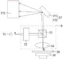
10-承载台;20-基板;31-激光源;32-激光调整部;33-分光镜;34-会聚透镜;35-光谱分析单元;351-光栅光谱仪;352-光谱分析仪;S-聚焦单元。10-carrying platform; 20-substrate; 31-laser source; 32-laser adjustment unit; 33-beam splitter; 34-converging lens; 35-spectral analysis unit; 351-grating spectrometer; 352-spectral analyzer; S-focus unit.
具体实施方式Detailed ways
如背景技术所述,激光切割晶圆的过程中易产生熔渣,导致晶圆平整度变差,影响晶圆后续工艺(例如晶圆键合工艺)。As mentioned in the background art, slag is likely to be generated during laser cutting of wafers, resulting in poor flatness of the wafer and affecting subsequent processes of the wafer (eg, wafer bonding process).
具体的,激光切割晶圆工艺中,在晶圆表面涂布一层水溶性激光保护液,激光产生的瞬时高温将硅衬底上面的激光保护液,金属,氧化层等材料气化以达到开槽目的,后续等离子刻蚀将硅衬底完全刻蚀实现晶圆切割,最后利用键合技术实现芯片与晶圆的键合。Specifically, in the process of laser cutting wafers, a layer of water-soluble laser protection liquid is coated on the surface of the wafer, and the instantaneous high temperature generated by the laser vaporizes the laser protection liquid, metal, oxide layer and other materials on the silicon substrate to achieve open For the purpose of grooving, the silicon substrate is completely etched by subsequent plasma etching to realize wafer cutting, and finally the bonding technology is used to realize the bonding of chips and wafers.
激光切割产生的瞬时高温将表面物质气化,气态物质挥发时遇冷凝结形成熔渣,激光切割时会有“铲雪效应”,切割时生成的熔渣沉积在切割道边缘形成山峰,熔渣导致晶圆平整度变差,影响后续键合制程。不同材料熔点不同,在切割时需要使用不同条件,例如金属与金属氧化物相比需要使用更高能量切割,若使用同一能量同时切割金属和低k材料层时,过高能量会产生大量熔渣堆积在晶圆表面影响晶圆平整度,低能量则会导致金属不能被切割透,两者都会影响后续制程。The instantaneous high temperature generated by laser cutting vaporizes the surface substances. When the gaseous substances volatilize, they condense to form slag. There will be a "snow removal effect" during laser cutting. The slag generated during cutting deposits on the edge of the cutting road to form a mountain peak. As a result, the flatness of the wafer is deteriorated, which affects the subsequent bonding process. Different materials have different melting points, and different conditions need to be used when cutting. For example, metals need to be cut with higher energy than metal oxides. If the same energy is used to cut metal and low-k material layers at the same time, excessive energy will produce a lot of slag Accumulation on the surface of the wafer affects the flatness of the wafer, and low energy will cause the metal to not be cut through, both of which will affect the subsequent process.
基于上述研究,本发明实施例提供了一种激光切割基板的方法。以下结合附图和具体实施例对本发明进一步详细说明。根据下面说明,本发明的优点和特征将更清楚。需要说明的是,附图均采用非常简化的形式且使用非精准的比例,仅用以方便、明晰地辅助说明本发明实施例的目的。Based on the above research, an embodiment of the present invention provides a method for laser cutting a substrate. The present invention will be described in further detail below in conjunction with the accompanying drawings and specific embodiments. The advantages and features of the present invention will become clearer from the following description. It should be noted that the drawings are all in a very simplified form and use imprecise scales, and are only used to facilitate and clearly assist the purpose of illustrating the embodiments of the present invention.
为了便于描述,本申请一些实施例可以使用诸如“在…上方”、“在…之下”、“顶部”、“下方”等空间相对术语,以描述如实施例各附图所示的一个元件或部件与另一个(或另一些)元件或部件之间的关系。应当理解的是,除了附图中描述的方位之外,空间相对术语还旨在包括装置在使用或操作中的不同方位。例如若附图中的装置被翻转,则被描述为在其它元件或部件“下方”或“之下”的元件或部件,随后将被定位为在其它元件或部件“上方”或“之上”。下文中的术语“第一”、“第二”、等用于在类似要素之间进行区分,且未必是用于描述特定次序或时间顺序。要理解,在适当情况下,如此使用的这些术语可替换。For the convenience of description, some embodiments of the present application may use spatially relative terms such as "above", "below", "top", "below" to describe an element as shown in each drawing of the embodiment or the relationship between a component and another (or other) elements or components. It will be understood that the spatially relative terms are intended to encompass different orientations of the device in use or operation in addition to the orientation depicted in the figures. For example, if the device in the figures is turned over, elements described as "below" or "beneath" other elements or features would then be oriented "above" or "over" the other elements or features. The terms "first", "second", etc. hereinafter are used to distinguish between similar elements, and are not necessarily used to describe a specific order or chronological order. It is to be understood that these terms so used are interchangeable under appropriate circumstances.
本发明实施例提供了一种激光切割基板的方法,如图1所示,包括:An embodiment of the present invention provides a method for laser cutting a substrate, as shown in FIG. 1 , including:
步骤S1、激光源发出的激光聚焦于基板上,所述基板上的不同材料层产生不同的反射光谱信号,所述反射光谱信号发送至光谱分析单元;Step S1, the laser light emitted by the laser source is focused on the substrate, and different material layers on the substrate generate different reflection spectrum signals, and the reflection spectrum signals are sent to the spectrum analysis unit;
步骤S2、所述光谱分析单元将所述反射光谱信号与标准图谱对比,计算出所述基板的不同材料层各自对应的折射率和消光系数,根据所述各自对应的折射率和消光系数模拟出所述基板上的材料分布三维模型;Step S2, the spectrum analysis unit compares the reflection spectrum signal with the standard spectrum, calculates the corresponding refractive index and extinction coefficient of the different material layers of the substrate, and simulates the A three-dimensional model of material distribution on the substrate;
步骤S3、激光控制器内预存入不同所述折射率和消光系数对应的激光切割参数,依据所述基板上的材料分布,选择对应的所述激光切割参数切割所述基板。Step S3, the laser controller pre-stores laser cutting parameters corresponding to different refractive indices and extinction coefficients, and selects the corresponding laser cutting parameters to cut the substrate according to the material distribution on the substrate.
具体的,如图2所示,激光源31发出的激光a经聚焦单元S聚焦于基板20上,基板20可以包括但不限于晶圆、玻璃、陶瓷等,其中,所述聚焦单元S包括激光调整部32、分光镜33和会聚透镜34,所述分光镜33与所述基板20之间设置所述会聚透镜34。所述激光a经所述激光调整部32调整后照射于所述分光镜33上,并经所述分光镜33反射至所述会聚透镜34上,经所述会聚透镜34将激光聚焦于所述基板20上,基板20可固定在承载台10上。Specifically, as shown in FIG. 2, the laser light a emitted by the
激光源31发射出的激光a相同的情况下,基板20上的不同材料层产生不同的反射光谱信号(反射光谱特征),所述反射光谱信号b经会聚透镜34及分光镜33发送至光谱分析单元35。光谱分析单元35包括光栅光谱仪351和光谱分析仪352。光栅光谱仪351获取基板反射光谱信号,并发送至光谱分析仪352,光谱分析仪352对反射光谱信号进行光谱分析。When the laser light a emitted by the
光谱分析仪352将所述反射光谱信号与标准图谱对比,计算出基板的不同材料层各自对应的折射率和消光系数,根据所述折射率和所述消光系数,模拟出基板切割道待切割层的材料分布三维模型。消光系数是待切割材料吸收特定波长的光的强烈程度的量度。The
激光控制器(未示出)内预存入不同所述折射率和消光系数对应的激光切割参数,依据所述基板上的材料分布,选择对应的所述激光切割参数切割所述基板。示例性的,所述基板的不同材料层包括:金属层、介质层和硅衬底中的至少一种。介质层例如包括低k材料层和氧化物层中的至少一种。介质层可根据需要设置,对介质层的材质不做限制。切割所述介质层的激光切割参数包括:激光束的脉冲重复频率范围500khz~2000khz,能量范围0.5W~5W,光斑宽度范围15μm~60μm,加工速度大于250mm/s,激光脉宽范围5ps~50ps。切割所述金属层的激光切割参数包括:激光束的脉冲重复频率范围500khz~1000khz,能量范围3W~10W,光斑宽度范围8μm~30μm,加工速度范围50mm/s~150mm/s,激光脉宽范围5ps~50ps。The laser controller (not shown) pre-stores laser cutting parameters corresponding to different refractive indices and extinction coefficients, and selects the corresponding laser cutting parameters to cut the substrate according to the material distribution on the substrate. Exemplarily, the different material layers of the substrate include: at least one of a metal layer, a dielectric layer and a silicon substrate. The dielectric layer includes, for example, at least one of a low-k material layer and an oxide layer. The medium layer can be set as required, and there is no restriction on the material of the medium layer. The laser cutting parameters for cutting the dielectric layer include: the pulse repetition frequency range of the laser beam is 500khz-2000khz, the energy range is 0.5W-5W, the spot width range is 15μm-60μm, the processing speed is greater than 250mm/s, and the laser pulse width range is 5ps-50ps . The laser cutting parameters for cutting the metal layer include: the pulse repetition frequency range of the laser beam is 500khz-1000khz, the energy range is 3W-10W, the spot width range is 8μm-30μm, the processing speed range is 50mm/s-150mm/s, the laser pulse width range 5ps~50ps.
激光切割方式是将激光汇聚于物体表面,当物体损伤阈值低于激光功率密度时,物体便会产生熔融、气化、离子化等物理或化学变化。当所用激光的功率足够大时,加工对象物即可沿着发生上述变化的位置断裂开,从而实现切割加工对象物的目的。切割所述基板时,所述激光聚焦于所述基板上的不同材料层中的功率密度大于各自材料层的损伤阈值。基板片上设有预定切割道,模拟出基板切割道待切割层的材料分布三维模型。激光通过沿所述预定切割道进行切割,将基板切割为多个芯片,激光的切割深度等于或小于基板的厚度。The laser cutting method is to focus the laser on the surface of the object. When the damage threshold of the object is lower than the laser power density, the object will undergo physical or chemical changes such as melting, gasification, and ionization. When the power of the laser used is large enough, the object to be processed can be broken along the position where the above changes occur, so as to achieve the purpose of cutting the object to be processed. When cutting the substrate, the power density of the laser focusing on different material layers on the substrate is greater than the damage threshold of the respective material layers. Predetermined cutting lines are arranged on the substrate sheet, and a three-dimensional model of material distribution of the layers to be cut by the substrate cutting lines is simulated. The laser cuts the substrate into a plurality of chips by cutting along the predetermined cutting line, and the cutting depth of the laser is equal to or smaller than the thickness of the substrate.
本实施例提供了一种激光切割基板的方法,根据基板的不同材料层各自对应的折射率和消光系数,选择对应的所述激光切割参数切割相应的材料层,实现不同材料层不同激光切割参数切割。每层材料层选择最适应该层的激光切割参数切割,能有效解决不同材料层损伤阈值不一样的问题,在切割后不会产生使用不合适的条件导致熔渣过高或部分材料未完全切割的问题,最终不会影响后续制程。This embodiment provides a method for laser cutting a substrate. According to the corresponding refractive index and extinction coefficient of different material layers of the substrate, the corresponding laser cutting parameters are selected to cut the corresponding material layer, so as to realize different laser cutting parameters for different material layers. cutting. Choose the most suitable laser cutting parameters for each layer of material, which can effectively solve the problem of different damage thresholds of different material layers, and will not cause excessive slag or incomplete cutting of some materials after cutting. The problem will not affect the subsequent process in the end.
本发明还提供一种激光切割装置,如图2所示,包括:The present invention also provides a laser cutting device, as shown in Figure 2, comprising:
激光源31、聚焦单元S、光谱分析单元35和激光控制器(未示出);
所述激光源31发出的激光经所述聚焦单元S聚焦于基板20上,所述基板20上的不同材料层产生不同的反射光谱信号,所述反射光谱信号b发送至所述光谱分单元35;The laser light emitted by the
所述光谱分析单元35将所述反射光谱信号与标准图谱对比,计算出所述不同材料层各自对应的折射率和消光系数,根据所述各自对应的折射率和消光系数模拟出所述基板上的材料分布三维模型;The
所述激光控制器内预存入不同所述折射率和所述消光系数对应的激光切割参数,依据所述基板上的材料分布,选择对应的所述激光切割参数切割所述基板。Laser cutting parameters corresponding to different refractive indices and extinction coefficients are pre-stored in the laser controller, and the corresponding laser cutting parameters are selected to cut the substrate according to the material distribution on the substrate.
具体的,所述聚焦单元S包括激光调整部32、分光镜33和会聚透镜34,所述分光镜33与所述基板20之间设置所述会聚透镜34;所述激光经所述激光调整部32调整后照射于所述分光镜33上,并经所述分光镜33反射至所述会聚透镜34上,经所述会聚透镜34将激光聚焦于所述基板20上。Specifically, the focusing unit S includes a
所述激光调整部32包括沿激光入射光路依次设置的光强调节部和扩束器;所述激光源发出的激光经所述光强调节部调节光强后,由所述扩束器进行扩束,激光经扩束后照射于所述分光镜33上。分光镜33将扩束后的激光反射至会聚透镜34上,会聚透镜34将激光聚焦于基板20上。示例性的,光强调节部可由半波片及偏振片组合;会聚透镜34的数值孔径为0.10~0.20,放大倍数为5~10倍。The
所述光谱分析单元35包括光栅光谱仪351和光谱分析仪352,激光源31发射出的激光a相同的情况下,基板20上不同材料层会产生不同的反射光谱信号(反射光谱特征),所述反射光谱信号b经会聚透镜34及分光镜33传至光栅光谱仪351。所述光栅光谱仪351获取所述基板上的不同材料层产生不同的反射光谱信号,并发送给所述光谱分析仪352,所述光谱分析仪352对所述反射光信号进行光谱分析。The
光谱分析仪将所述反射光谱信号与标准图谱对比,计算出基板的待切割层不同材料层各自对应的折射率和消光系数,根据所述折射率和所述消光系数,模拟出基板切割道待切割层的材料分布三维模型;The spectrum analyzer compares the reflection spectrum signal with the standard spectrum, calculates the corresponding refractive index and extinction coefficient of the different material layers of the substrate to be cut, and simulates the cutting line of the substrate according to the refractive index and the extinction coefficient. 3D model of material distribution in the cutting layer;
所述激光控制器(未示出)内预存入不同所述折射率和所述消光系数对应的激光切割参数,依据所述基板上的材料分布,选择对应的所述激光切割参数切割所述基板。Laser cutting parameters corresponding to different refractive indices and extinction coefficients are pre-stored in the laser controller (not shown), and the corresponding laser cutting parameters are selected to cut the substrate according to the material distribution on the substrate .
综上所述,本发明提供一种激光切割基板的方法及激光切割装置,包括:激光源发出的激光聚焦于基板上,基板上的不同材料层产生不同的反射光谱信号,反射光谱信号发送至光谱分析单元;光谱分析单元将反射光谱信号与标准图谱对比,计算出基板的不同材料层各自对应的折射率和消光系数,根据各自对应的折射率和消光系数模拟出基板上的材料分布三维模型;依据基板上的材料分布,选择对应的激光切割参数切割基板。根据基板的不同材料层各自对应的折射率和消光系数,选择对应的激光切割参数切割相应的材料层,实现不同材料层不同激光切割参数切割,有效解决不同材料层损伤阈值不一样的问题,在切割后不会产生熔渣过高或部分材料未完全切割的问题,不影响后续制程。To sum up, the present invention provides a method and a laser cutting device for laser cutting a substrate, including: laser light emitted by a laser source is focused on the substrate, different material layers on the substrate generate different reflection spectrum signals, and the reflection spectrum signals are sent to Spectral analysis unit; the spectral analysis unit compares the reflection spectrum signal with the standard spectrum, calculates the corresponding refractive index and extinction coefficient of different material layers of the substrate, and simulates the three-dimensional model of material distribution on the substrate according to the corresponding refractive index and extinction coefficient ; According to the material distribution on the substrate, select the corresponding laser cutting parameters to cut the substrate. According to the corresponding refractive index and extinction coefficient of different material layers of the substrate, select the corresponding laser cutting parameters to cut the corresponding material layers, realize the cutting of different material layers with different laser cutting parameters, and effectively solve the problem of different damage thresholds of different material layers. After cutting, there will be no problem of excessive slag or incomplete cutting of some materials, and will not affect the subsequent process.
本说明书中各个实施例采用递进的方式描述,每个实施例重点说明的都是与其他实施例的不同之处,各个实施例之间相同相似部分互相参见即可。对于实施例公开的方法而言,由于与实施例公开的器件相对应,所以描述的比较简单,相关之处参见方法部分说明即可。Each embodiment in this specification is described in a progressive manner, each embodiment focuses on the difference from other embodiments, and the same and similar parts of each embodiment can be referred to each other. As for the methods disclosed in the embodiments, since they correspond to the devices disclosed in the embodiments, the description is relatively simple, and for the related parts, please refer to the description of the methods.
上述描述仅是对本发明较佳实施例的描述,并非对本发明权利范围的任何限定,任何本领域技术人员在不脱离本发明的精神和范围内,都可以利用上述揭示的方法和技术内容对本发明技术方案做出可能的变动和修改,因此,凡是未脱离本发明技术方案的内容,依据本发明的技术实质对以上实施例所作的任何简单修改、等同变化及修饰,均属于本发明技术方案的保护范围。The above description is only a description of the preferred embodiments of the present invention, and is not any limitation to the scope of rights of the present invention. Anyone skilled in the art can use the methods and technical contents disclosed above to analyze the present invention without departing from the spirit and scope of the present invention. Possible changes and modifications are made in the technical solution. Therefore, any simple modification, equivalent change and modification made to the above embodiments according to the technical essence of the present invention, which do not depart from the content of the technical solution of the present invention, all belong to the technical solution of the present invention. protected range.
Claims (10)
Priority Applications (1)
| Application Number | Priority Date | Filing Date | Title |
|---|---|---|---|
| CN202211348971.6ACN116117342B (en) | 2022-10-31 | 2022-10-31 | Method for laser cutting substrate and laser cutting device |
Applications Claiming Priority (1)
| Application Number | Priority Date | Filing Date | Title |
|---|---|---|---|
| CN202211348971.6ACN116117342B (en) | 2022-10-31 | 2022-10-31 | Method for laser cutting substrate and laser cutting device |
Publications (2)
| Publication Number | Publication Date |
|---|---|
| CN116117342Atrue CN116117342A (en) | 2023-05-16 |
| CN116117342B CN116117342B (en) | 2024-11-12 |
Family
ID=86305200
Family Applications (1)
| Application Number | Title | Priority Date | Filing Date |
|---|---|---|---|
| CN202211348971.6AActiveCN116117342B (en) | 2022-10-31 | 2022-10-31 | Method for laser cutting substrate and laser cutting device |
Country Status (1)
| Country | Link |
|---|---|
| CN (1) | CN116117342B (en) |
Citations (4)
| Publication number | Priority date | Publication date | Assignee | Title |
|---|---|---|---|---|
| CN1663038A (en)* | 2002-04-19 | 2005-08-31 | Xsil技术有限公司 | laser processing |
| CN104814828A (en)* | 2015-05-21 | 2015-08-05 | 中国科学院光电研究院 | Femtosecond laser system and method for determining focus position of laser in cornea tissue |
| CN105044045A (en)* | 2015-05-21 | 2015-11-11 | 中国科学院光电研究院 | Laser system and method of detecting cornea cutting threshold value through spectrum analysis |
| CN113953689A (en)* | 2021-12-16 | 2022-01-21 | 湖北三维半导体集成创新中心有限责任公司 | A method of cutting wafers |
- 2022
- 2022-10-31CNCN202211348971.6Apatent/CN116117342B/enactiveActive
Patent Citations (5)
| Publication number | Priority date | Publication date | Assignee | Title |
|---|---|---|---|---|
| CN1663038A (en)* | 2002-04-19 | 2005-08-31 | Xsil技术有限公司 | laser processing |
| CN104814828A (en)* | 2015-05-21 | 2015-08-05 | 中国科学院光电研究院 | Femtosecond laser system and method for determining focus position of laser in cornea tissue |
| CN105044045A (en)* | 2015-05-21 | 2015-11-11 | 中国科学院光电研究院 | Laser system and method of detecting cornea cutting threshold value through spectrum analysis |
| DE102016101483A1 (en)* | 2015-05-21 | 2016-11-24 | Academy Of Opto-Electronics, Chinese Academy Of Sciences | Laser system for detecting a corneal ablation threshold potential by means of spectral analysis of the laser-induced plasma and detection method |
| CN113953689A (en)* | 2021-12-16 | 2022-01-21 | 湖北三维半导体集成创新中心有限责任公司 | A method of cutting wafers |
Also Published As
| Publication number | Publication date |
|---|---|
| CN116117342B (en) | 2024-11-12 |
Similar Documents
| Publication | Publication Date | Title |
|---|---|---|
| US7994450B2 (en) | Debris minimization and improved spatial resolution in pulsed laser ablation of materials | |
| JP4384412B2 (en) | Method and system for processing a device, method and system for modeling a device, and device | |
| JP4391524B2 (en) | Link processing method and laser system using laser pulses with a specially shaped power profile. | |
| JP2004526335A (en) | Two-stage laser cutting of wafer | |
| US7599048B2 (en) | Optical emission spectroscopy process monitoring and material characterization | |
| KR20080039453A (en) | Control of individual vias formed during energy monitoring or laser micromachining | |
| JP2015037808A (en) | Method and apparatus for performing laser filamentation inside a transparent material | |
| KR102689547B1 (en) | Method for laser forming transparent articles from transparent mother sheets and processing transparent articles in situ | |
| JP2022520201A (en) | Laser machining of transparent workpieces | |
| JP2018523291A (en) | Method for scribing semiconductor workpiece | |
| JP6076601B2 (en) | Laser processing method, semiconductor device manufacturing method, and laser processing apparatus | |
| JP2006524828A (en) | Single-wavelength ellipsometry for measuring the thickness of thin films on multilayer substrates. | |
| Kong et al. | Femtosecond laser induced damage of pulse compression gratings | |
| JPH04130752A (en) | Manufacture of integrated circuit | |
| CN107214419B (en) | Method and device for processing wafer by laser | |
| JPH11121576A (en) | Equipment and method for repairing semiconductor wafer | |
| CN116117342A (en) | Method for cutting substrate by laser and laser cutting device | |
| JPH07204876A (en) | Device for drilling hole in protective film on ic surface and method for drilling hole by using the method | |
| KR100843411B1 (en) | Laser processing device and substrate cutting method | |
| Mingareev et al. | Laser Dicing of Silicon and Electronics Substrates | |
| JP2024136181A (en) | Laser processing method, laser processing device, and laser light source | |
| CN113226632A (en) | Laser system for cutting semiconductor structure and operation method thereof | |
| CN115533338A (en) | Laser dicing apparatus and wafer dicing method | |
| JP2011177735A (en) | Laser beam drilling method | |
| JP2003236688A (en) | Laser beam machining device |
Legal Events
| Date | Code | Title | Description |
|---|---|---|---|
| PB01 | Publication | ||
| PB01 | Publication | ||
| SE01 | Entry into force of request for substantive examination | ||
| SE01 | Entry into force of request for substantive examination | ||
| CB02 | Change of applicant information | ||
| CB02 | Change of applicant information | Country or region after:China Address after:430205 No.18, Gaoxin 4th Road, Donghu Development Zone, Wuhan City, Hubei Province Applicant after:Wuhan Xinxin Integrated Circuit Co.,Ltd. Address before:430205 No.18, Gaoxin 4th Road, Donghu Development Zone, Wuhan City, Hubei Province Applicant before:Wuhan Xinxin Semiconductor Manufacturing Co.,Ltd. Country or region before:China | |
| GR01 | Patent grant | ||
| GR01 | Patent grant |