CN116115906A - Communication method of electric stimulator and electric stimulator - Google Patents
Communication method of electric stimulator and electric stimulatorDownload PDFInfo
- Publication number
- CN116115906A CN116115906ACN202310115736.2ACN202310115736ACN116115906ACN 116115906 ACN116115906 ACN 116115906ACN 202310115736 ACN202310115736 ACN 202310115736ACN 116115906 ACN116115906 ACN 116115906A
- Authority
- CN
- China
- Prior art keywords
- chip
- electrode
- sub
- power supply
- supply unit
- Prior art date
- Legal status (The legal status is an assumption and is not a legal conclusion. Google has not performed a legal analysis and makes no representation as to the accuracy of the status listed.)
- Granted
Links
Images


Classifications
- A—HUMAN NECESSITIES
- A61—MEDICAL OR VETERINARY SCIENCE; HYGIENE
- A61N—ELECTROTHERAPY; MAGNETOTHERAPY; RADIATION THERAPY; ULTRASOUND THERAPY
- A61N1/00—Electrotherapy; Circuits therefor
- A61N1/18—Applying electric currents by contact electrodes
- A61N1/32—Applying electric currents by contact electrodes alternating or intermittent currents
- A61N1/36—Applying electric currents by contact electrodes alternating or intermittent currents for stimulation
- A61N1/36014—External stimulators, e.g. with patch electrodes
- A61N1/36025—External stimulators, e.g. with patch electrodes for treating a mental or cerebral condition
- A—HUMAN NECESSITIES
- A61—MEDICAL OR VETERINARY SCIENCE; HYGIENE
- A61N—ELECTROTHERAPY; MAGNETOTHERAPY; RADIATION THERAPY; ULTRASOUND THERAPY
- A61N1/00—Electrotherapy; Circuits therefor
- A61N1/02—Details
- A61N1/04—Electrodes
- A61N1/05—Electrodes for implantation or insertion into the body, e.g. heart electrode
- A61N1/0526—Head electrodes
- A61N1/0529—Electrodes for brain stimulation
- A61N1/0534—Electrodes for deep brain stimulation
- A—HUMAN NECESSITIES
- A61—MEDICAL OR VETERINARY SCIENCE; HYGIENE
- A61N—ELECTROTHERAPY; MAGNETOTHERAPY; RADIATION THERAPY; ULTRASOUND THERAPY
- A61N1/00—Electrotherapy; Circuits therefor
- A61N1/18—Applying electric currents by contact electrodes
- A61N1/32—Applying electric currents by contact electrodes alternating or intermittent currents
- A61N1/36—Applying electric currents by contact electrodes alternating or intermittent currents for stimulation
- A61N1/3605—Implantable neurostimulators for stimulating central or peripheral nerve system
- A61N1/3606—Implantable neurostimulators for stimulating central or peripheral nerve system adapted for a particular treatment
- A61N1/36064—Epilepsy
- A—HUMAN NECESSITIES
- A61—MEDICAL OR VETERINARY SCIENCE; HYGIENE
- A61N—ELECTROTHERAPY; MAGNETOTHERAPY; RADIATION THERAPY; ULTRASOUND THERAPY
- A61N1/00—Electrotherapy; Circuits therefor
- A61N1/18—Applying electric currents by contact electrodes
- A61N1/32—Applying electric currents by contact electrodes alternating or intermittent currents
- A61N1/36—Applying electric currents by contact electrodes alternating or intermittent currents for stimulation
- A61N1/3605—Implantable neurostimulators for stimulating central or peripheral nerve system
- A61N1/3606—Implantable neurostimulators for stimulating central or peripheral nerve system adapted for a particular treatment
- A61N1/36067—Movement disorders, e.g. tremor or Parkinson disease
- A—HUMAN NECESSITIES
- A61—MEDICAL OR VETERINARY SCIENCE; HYGIENE
- A61N—ELECTROTHERAPY; MAGNETOTHERAPY; RADIATION THERAPY; ULTRASOUND THERAPY
- A61N1/00—Electrotherapy; Circuits therefor
- A61N1/18—Applying electric currents by contact electrodes
- A61N1/32—Applying electric currents by contact electrodes alternating or intermittent currents
- A61N1/36—Applying electric currents by contact electrodes alternating or intermittent currents for stimulation
- A61N1/3605—Implantable neurostimulators for stimulating central or peripheral nerve system
- A61N1/3606—Implantable neurostimulators for stimulating central or peripheral nerve system adapted for a particular treatment
- A61N1/36082—Cognitive or psychiatric applications, e.g. dementia or Alzheimer's disease
- A61N1/36089—Addiction or withdrawal from substance abuse such as alcohol or drugs
- G—PHYSICS
- G06—COMPUTING OR CALCULATING; COUNTING
- G06F—ELECTRIC DIGITAL DATA PROCESSING
- G06F13/00—Interconnection of, or transfer of information or other signals between, memories, input/output devices or central processing units
- G06F13/38—Information transfer, e.g. on bus
- G06F13/42—Bus transfer protocol, e.g. handshake; Synchronisation
- G06F13/4282—Bus transfer protocol, e.g. handshake; Synchronisation on a serial bus, e.g. I2C bus, SPI bus
Landscapes
- Health & Medical Sciences (AREA)
- Neurology (AREA)
- Engineering & Computer Science (AREA)
- Neurosurgery (AREA)
- Life Sciences & Earth Sciences (AREA)
- Nuclear Medicine, Radiotherapy & Molecular Imaging (AREA)
- Veterinary Medicine (AREA)
- Public Health (AREA)
- General Health & Medical Sciences (AREA)
- Animal Behavior & Ethology (AREA)
- Radiology & Medical Imaging (AREA)
- Biomedical Technology (AREA)
- Psychology (AREA)
- Child & Adolescent Psychology (AREA)
- Psychiatry (AREA)
- Hospice & Palliative Care (AREA)
- Developmental Disabilities (AREA)
- Heart & Thoracic Surgery (AREA)
- Theoretical Computer Science (AREA)
- Social Psychology (AREA)
- Addiction (AREA)
- Bioinformatics & Cheminformatics (AREA)
- Cardiology (AREA)
- Physics & Mathematics (AREA)
- General Engineering & Computer Science (AREA)
- General Physics & Mathematics (AREA)
- Biophysics (AREA)
- Electrotherapy Devices (AREA)
Abstract
Description
Translated fromChinese技术领域technical field
本发明涉及植入式医疗器械技术领域,尤其是涉及一种电刺激器的通信方法和电刺激器。The invention relates to the technical field of implantable medical devices, in particular to a communication method of an electric stimulator and the electric stimulator.
背景技术Background technique
脑深部电刺激器(DBS,Deep Brain Stimulation)可以有效治疗运动障碍类疾病,也可以用于精神疾病的治疗,例如可用于帕金森病、癫痫、抑郁、成瘾性疾病等的治疗。Deep Brain Stimulation (DBS, Deep Brain Stimulation) can effectively treat movement disorders, and can also be used for the treatment of mental diseases, such as Parkinson's disease, epilepsy, depression, and addictive diseases.
脑深部电刺激器的电极是脑深部电刺激器中的重要组成部分,电极一般通过导线与植入式供电单元电连接,然而,对于高密度DBS电极而言,其电极刺激端(电极部)上的刺激位点的数量一般多于导线的数量,如何实现植入式供电单元与电极刺激端之间的通信,是本领域技术人员需要解决的难题。The electrodes of the deep brain electrical stimulator are an important part of the deep brain electrical stimulator. The electrodes are generally electrically connected to the implanted power supply unit through wires. However, for high-density DBS electrodes, the electrode stimulation end (electrode part) The number of stimulation sites on the electrode is generally more than the number of wires. How to realize the communication between the implantable power supply unit and the electrode stimulation terminal is a difficult problem to be solved by those skilled in the art.
发明内容Contents of the invention
本发明旨在至少解决现有技术中存在的技术问题之一。为此,本发明的一个目的在于提出一种电刺激器的通信方法,植入式供电单元与第一子电极或第二子电极之间的信号传输简单高效。The present invention aims to solve at least one of the technical problems existing in the prior art. Therefore, an object of the present invention is to provide a communication method for an electrical stimulator, and the signal transmission between the implanted power supply unit and the first sub-electrode or the second sub-electrode is simple and efficient.
本发明的另一个目的在于提出一种采用上述通信方法的电刺激器。Another object of the present invention is to provide an electrical stimulator using the above communication method.
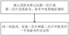
根据本发明第一方面实施例的电刺激器的通信方法,所述电刺激器包括植入式供电单元、第一芯片和第二芯片,所述第一芯片和第二芯片通过多个导线与所述植入式供电单元电连接,所述第一芯片连接第一子电极,所述第二芯片连接第二子电极;According to the communication method of the electric stimulator according to the embodiment of the first aspect of the present invention, the electric stimulator includes an implantable power supply unit, a first chip and a second chip, and the first chip and the second chip communicate with each other through a plurality of wires. The implantable power supply unit is electrically connected, the first chip is connected to the first sub-electrode, and the second chip is connected to the second sub-electrode;
所述通信方法包括以下步骤:The communication method includes the following steps:
所述植入式供电单元向所述第一芯片或所述第二芯片发送命令,所述命令中包括地址识识码,以确定对所述命令作出应答的芯片;The implantable power supply unit sends a command to the first chip or the second chip, and the command includes an address identification code to determine the chip that responds to the command;
同一时段内,仅所述第一芯片和所述第二芯片中的其中一个对所述命令作出应答。During the same time period, only one of the first chip and the second chip responds to the command.
根据本发明第一方面实施例的电刺激器的通信方法,可以快速区分对命令作出应答的第一芯片和第二芯片,从而方便了植入式供电单元与第一子电极和第二子电极的通讯。此外,可以使同一植入式供电单元的命令准确地传输至对应的第一子电极或第二子电极处,本发明通信方式简单高效,尤其适用于高密度电极,刺激精度较高。According to the communication method of the electrical stimulator of the embodiment of the first aspect of the present invention, the first chip and the second chip that respond to the command can be quickly distinguished, thereby facilitating the communication between the implanted power supply unit and the first sub-electrode and the second sub-electrode communication. In addition, commands from the same implanted power supply unit can be accurately transmitted to the corresponding first sub-electrode or second sub-electrode. The communication method of the present invention is simple and efficient, especially suitable for high-density electrodes, and has high stimulation accuracy.
根据本发明的一些实施例,所述植入式供电单元与第一芯片及第二芯片之间的通信方式为串行通信。According to some embodiments of the present invention, the communication mode between the implantable power supply unit and the first chip and the second chip is serial communication.
根据本发明的一些实施例,所述植入式供电单元与第一芯片及第二芯片之间的通讯协议为I2C、SMBus、RS232或RS485。According to some embodiments of the present invention, the communication protocol between the implantable power supply unit and the first chip and the second chip is I2 C, SMBus, RS232 or RS485.
根据本发明的一些实施例,所述通信方法包括:According to some embodiments of the present invention, the communication method includes:
所述植入式供电单元向所述第一芯片和所述第二芯片发送命令,形成信号下行;The implantable power supply unit sends commands to the first chip and the second chip to form a downlink signal;
同一时段内,仅所述第一芯片或所述第二芯片中的其中一个对所述命令作出应答,形成信号上行;In the same period of time, only one of the first chip or the second chip responds to the command, forming an upstream signal;
所述信号上行的通路和所述信号下行的通路上分别增加电平转换器。A level shifter is respectively added to the upstream path of the signal and the downstream path of the signal.
根据本发明的一些实施例,所述导线包括至少四根引线,至少四根所述引线包括两根电源线和两根数据线。According to some embodiments of the present invention, the wires include at least four lead wires, and the at least four lead wires include two power lines and two data lines.
根据本发明的一些实施例,所述数据线上的电压是对称的交流电。According to some embodiments of the present invention, the voltage on the data line is a symmetrical alternating current.
根据本发明第二方面实施例的电刺激器,所述电刺激器工作时执行根据上述第一方面实施例所述的电刺激器的通信方法。According to the electrical stimulator of the embodiment of the second aspect of the present invention, the electrical stimulator implements the communication method of the electrical stimulator according to the embodiment of the first aspect when working.
根据本发明的一些实施例,所述导线通过连接器连接第一芯片和第二芯片,所述连接器上开设有适于导线嵌入的理线槽以及沿厚度方向延伸的导电销,所述导电销同时连接位于其上方的第一芯片和位于其下方的第二芯片。According to some embodiments of the present invention, the wire is connected to the first chip and the second chip through a connector, and the connector is provided with a wire management groove suitable for embedding the wire and a conductive pin extending along the thickness direction, and the conductive pin The pins simultaneously connect the first chip above it and the second chip below it.
根据本发明的一些实施例,所述第一子电极和所述第二子电极卷曲并贴附于电极支撑柱上以形成电极部。According to some embodiments of the present invention, the first sub-electrode and the second sub-electrode are crimped and attached to an electrode support column to form an electrode part.
根据本发明的一些实施例,所述电刺激器具体为脑深部电刺激器。According to some embodiments of the present invention, the electrical stimulator is specifically a deep brain electrical stimulator.
本发明的附加方面和优点将在下面的描述中部分给出,部分将从下面的描述中变得明显,或通过本发明的实践了解到。Additional aspects and advantages of the invention will be set forth in the description which follows, and in part will be obvious from the description, or may be learned by practice of the invention.
附图说明Description of drawings
本发明的上述和/或附加的方面和优点从结合下面附图对实施例的描述中将变得明显和容易理解,其中:The above and/or additional aspects and advantages of the present invention will become apparent and understandable from the description of the embodiments in conjunction with the following drawings, wherein:
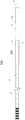
图1是根据本发明实施例的电极结构的示意图;1 is a schematic diagram of an electrode structure according to an embodiment of the present invention;
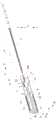
图2是根据本发明实施例的电极结构的分解图;2 is an exploded view of an electrode structure according to an embodiment of the present invention;
图3是图2中圈示的D区域的放大图;Figure 3 is an enlarged view of the area D circled in Figure 2;
图4是图2中圈示的E区域的放大图;Figure 4 is an enlarged view of the area E circled in Figure 2;
图5是图2中圈示的F区域的放大图;Figure 5 is an enlarged view of the F area circled in Figure 2;
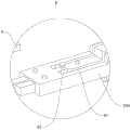
图6是根据本发明实施例的连接器的示意图;6 is a schematic diagram of a connector according to an embodiment of the present invention;
图7是根据本发明实施例的另一个角度的连接器的示意图;7 is a schematic diagram of a connector at another angle according to an embodiment of the present invention;
图8是根据本发明实施例的电极结构的俯视图;8 is a top view of an electrode structure according to an embodiment of the present invention;
图9是图8中圈示的G区域的示意图;Fig. 9 is a schematic diagram of the G area circled in Fig. 8;
图10是根据本发明实施例的另一个角度的电极结构的示意图;10 is a schematic diagram of an electrode structure from another angle according to an embodiment of the present invention;
图11是图10中圈示的H区域的示意图;Figure 11 is a schematic diagram of the H area circled in Figure 10;
图12是根据本发明实施例的电刺激器的通信方法的流程图;Fig. 12 is a flowchart of a communication method of an electrical stimulator according to an embodiment of the present invention;
图13是根据本发明实施例的电刺激器的通信方法的信号传输的流程图。Fig. 13 is a flow chart of signal transmission in the communication method of the electrical stimulator according to the embodiment of the present invention.
附图标记:Reference signs:
100、电极结构;100. Electrode structure;
200、连接器;200, connector;
201、第一段;2012、导针定位孔;201. The first paragraph; 2012. Guide pin positioning hole;
202、第二段;2021、台阶结构;2023、通孔;205、导针;202, second section; 2021, step structure; 2023, through hole; 205, guide pin;
1a、电极部;1、电极支撑柱;11、第一子支撑段;1a, the electrode part; 1, the electrode support column; 11, the first sub-support section;
12、第二子支撑段;121、定位孔;12. The second sub-support section; 121. Positioning holes;
13、凹槽;14、限位孔;13. Groove; 14. Limit hole;
21、第一子电极;22、第二子电极;21. The first sub-electrode; 22. The second sub-electrode;
23、连接线缆;24、折边;3、注胶件;23. Connecting cables; 24. Hemming; 3. Plastic injection parts;
4、套管;5、导线;4. Casing; 5. Conductor;
6、第一芯片;7、第二芯片;6. The first chip; 7. The second chip;
81、理线槽;82、导电销。81, cable management trough; 82, conductive pin.
具体实施方式Detailed ways
下面详细描述本发明的实施例,参考附图描述的实施例是示例性的,下面参考图1-图11描述根据本发明第一方面实施例的电刺激器的通信方法。The embodiments of the present invention are described in detail below, and the embodiments described with reference to the accompanying drawings are exemplary, and the communication method of the electrical stimulator according to the embodiment of the first aspect of the present invention is described below with reference to FIGS. 1-11 .
电刺激器(图未示出)包括植入式供电单元(图未示出)、第一芯片6和第二芯片7,第一芯片6和第二芯片7通过多个导线5与植入式供电单元电连接,第一芯片6连接第一子电极21,第二芯片7连接第二子电极22。例如,第一子电极21和第二子电极22为高密度柔性电极2,第一子电极21和第二子电极22上均设置有多个刺激位点(图未示出)。在本发明的描述中,“多个”的含义是两个或两个以上。第一芯片6和第二芯片7可以为ASIC(专用集成电路)芯片。第一子电极21和第二子电极22上优选设置数十、数百甚至更多刺激位点,从而能形成相对于现有技术更高密度的柔性电极。第一子电极21和第二子电极22优选通过MEMS工艺制造形成带状结构,且最终形成所需电极尺寸(如标准DBS电极尺寸)。此外,植入式供电单元可以设置电源,也可以采用外部件并通过无线射频方式供电,并能作为主控装置使用。The electrical stimulator (not shown) includes an implanted power supply unit (not shown), a
由此,第一子电极21和第二子电极22的多个刺激位点可以通过第一芯片6、第二芯片7和导线5与植入式供电单元通讯。以上刺激位点还能用作记录位点使用,此外还可以在各子电极上额外设置记录位点,均涵盖在本发明的技术方案内。Thus, multiple stimulation sites of the
此外,与传统的电极结构100相比,第一子电极21和第二子电极22的刺激位点较多,触点面积较小,不易刺激不必要的区域,从而可以减少使用电刺激器的副作用。另外,采用柔性电极2,可以实现定向刺激、分区刺激以及多靶点刺激,从而大幅提高了电刺激器的刺激精度,降低了对电极植入精度的依赖性,减少了电刺激产生的并发症,进而可以确保治疗效果,实现精准治疗。例如,配合记录电极使用,可精准采集脑神经活动信号,为临床医生提供客观参数,可实现个性化闭环控制治疗。In addition, compared with the
如图1、图2和图12所示,根据本发明第一方面实施例的电刺激器的通信方法,包括以下步骤:As shown in Figure 1, Figure 2 and Figure 12, the communication method of the electrical stimulator according to the embodiment of the first aspect of the present invention includes the following steps:
植入式供电单元向第一芯片6或第二芯片7发送命令,命令中包括地址识别码,以确定对命令作出应答的芯片;The implantable power supply unit sends a command to the
同一时段内,仅第一芯片6和第二芯片7中的其中一个对命令作出应答。During the same period, only one of the
由此,通过地址识别码,可以区分对命令作出应答的第一芯片6和第二芯片7,从而方便植入式供电单元与第一子电极21和第二子电极22的通讯。此外,通过使第一芯片6和第二芯片7中的其中一个对命令作出应答,可以使植入式供电单元的命令准确地传输至对应的第一子电极21或第二子电极22处,提高了电刺激器的信号传输的准确度,进而提高了电刺激器的刺激精度。Therefore, through the address identification code, the
根据本发明第一方面实施例的电刺激器的通信方法,可以使同一植入式供电单元的命令准确地传输至对应的第一子电极21或第二子电极22处,通信方式简单高效,尤其适用于高密度电极,刺激精度较高。According to the communication method of the electrical stimulator of the embodiment of the first aspect of the present invention, the command of the same implantable power supply unit can be accurately transmitted to the corresponding first sub-electrode 21 or second sub-electrode 22, and the communication method is simple and efficient. It is especially suitable for high-density electrodes with high stimulation accuracy.
根据本发明的一些实施例,植入式供电单元与第一芯片6及第二芯片7之间的通信方式为串行通信。由此,有利于植入式供电单元与第一芯片6及第二芯片7之间的信号传输,并且传输线少,可以使电刺激器的尺寸较小,组装工艺简单,成本低。According to some embodiments of the present invention, the communication mode between the implantable power supply unit and the
可选地,植入式供电单元与第一芯片6及第二芯片7之间的通讯协议为I2C、SMBus、RS232或RS485等。由此,通过采用上述的通讯协议,有利于植入式供电单元与第一芯片6和第二芯片7之间的信号顺利地传输,有利于电刺激器的正常使用。Optionally, the communication protocol between the implantable power supply unit and the
根据本发明的一些实施例,结合图13,植入式供电单元向第一芯片6或第二芯片7发送命令,形成信号下行;According to some embodiments of the present invention, referring to FIG. 13 , the implantable power supply unit sends a command to the
同一时段内,仅第一芯片6和第二芯片7中的其中一个对命令作出应答,形成信号上行;In the same period of time, only one of the
信号上行的通路和信号下行的通路上分别增加电平转换器。Level converters are respectively added to the signal upstream path and the signal downstream path.
当电刺激器植入人体组织时,第一芯片6或第二芯片7接收到植入式供电单元的命令后,输出命令至第一子电极21或第二子电极22,从而植入式供电单元可以发送定向电刺激至相应功能区,达到精准治疗的效果。此外,在信号上行的通路和信号下行的通路分别增加电平转换器,实现对信号的电平转换,以便于系统开发,可以用于帕金森、肌张力障碍、震颤和冻结步态等运动障碍,另外也能作为药物成瘾、抑郁症的替代治疗方案。When the electric stimulator is implanted in human tissue, after receiving the command of the implanted power supply unit, the
可选地,导线5包括至少四根引线,四根引线包括两根电源线和两根数据线。如此设置,数据线可以用于命令信号的传输,电源线用于能量信号的传输,从而保证了导线5的正常使用,同时引线数量较少,可以减小导线5的尺寸。本发明实施例的电源线以对称的交流电形式存在。Optionally, the
根据本发明的一些实施例,数据线上的电压是对称的交流电。由此,信号传输较为稳定,有利于数据线的信号传输,同时可降低直流泄露风险,提高安全性。According to some embodiments of the present invention, the voltage on the data line is a symmetrical alternating current. Therefore, the signal transmission is relatively stable, which is beneficial to the signal transmission of the data line, and at the same time can reduce the risk of DC leakage and improve safety.
根据本发明第二方面实施例的电刺激器,电刺激器工作时执行根据上述第一方面实施例的电刺激器的通信方法。According to the electrical stimulator of the embodiment of the second aspect of the present invention, when the electrical stimulator is working, the communication method of the electrical stimulator according to the embodiment of the first aspect above is executed.
根据本发明实施例的电刺激器,采用上述的电刺激器的通讯方法,可以快速准确地将植入式供电单元的命令例如电刺激传输至第一电极或第二电极,也可以及时地收到第一芯片6或第二芯片7的信号反馈,从而实现电极结构100与植入式供电单元的有效连接,并且可以保证对单个电极进行刺激波形控制,从而提高刺激方向的精确控制,实现更优的刺激效果。According to the electric stimulator of the embodiment of the present invention, the above-mentioned communication method of the electric stimulator can be used to quickly and accurately transmit the command of the implanted power supply unit, such as electric stimulation, to the first electrode or the second electrode, and can also receive the order in time. The signal feedback to the
根据本发明的一些实施例,参照图2、图6和图7,导线5通过连接器200连接第一芯片6和第二芯片7,连接器200上开设有适于导线5嵌入的理线槽81以及沿厚度方向延伸的导电销82,导电销82同时连接位于其上方的第一芯片6和位于其下方的第二芯片7。According to some embodiments of the present invention, with reference to Fig. 2, Fig. 6 and Fig. 7, the
例如,在图6和图7的示例中,连接器200的上表面和下表面均形成有理线槽81。由此,理线槽81对导线5具有支撑作用和固定作用,从而有利于导线5与第一芯片6和第二芯片7的连接,连接稳定。此外,电刺激器的第一芯片6位于连接器200的上方,电刺激器的第二芯片7位于连接器200的下方,第一芯片6和第二芯片7可以通过导电销82电连接。For example, in the example of FIG. 6 and FIG. 7 , the upper surface and the lower surface of the
根据本发明的一些实施例,第一子电极21和第二子电极22卷曲并贴附于电极支撑柱1上以形成电极部。第一子电极21和第二子电极22的结构大致相同,第一子电极21和第二子电极22均沿电极支撑柱1的周向卷曲并贴附于电极支撑柱1的外周侧,第一子电极21和第二子电极22的长边均沿电极支撑柱1的轴向设置。例如,在图2的示例中,第一子电极21、第二子电极22和电极支撑柱1均沿轴向(即左右方向,例如,图2中箭头A所指的方向)延伸,第一子电极21和第二子电极22沿电极支撑柱11的周向排布。如此设置,电极支撑柱1对第一子电极21和第二子电极22具有支撑作用。此外,第一子电极21和第二子电极22的结构简单,生产难度较小,方便了第一子电极21和第二子电极22的生产加工,并且有利于电极部的装配。According to some embodiments of the present invention, the
根据本发明的一些实施例,电刺激器可以为脑深部电刺激器(图未示出),还可以为脊髓刺激器或其它可能电刺激器。According to some embodiments of the present invention, the electrical stimulator may be a deep brain electrical stimulator (not shown in the figure), and may also be a spinal cord stimulator or other possible electrical stimulators.
参照图2,第一子电极21和第二子电极22上均设置有连接多个刺激位点的连接线缆23,连接线缆23适于与电刺激器的植入式供电单元电连接。具体地,连接线缆23的一端与多个刺激位点电连接,连接线缆23的另一端与植入式供电单元电连接。由此,第一子电极21和第二子电极22的多个刺激位点可以通过连接线缆23与植入式供电单元电连接,有利于植入式供电单元与柔性电极之间的信号传输。Referring to FIG. 2 , the
根据本发明的一些实施例,参照图2,电极支撑柱1包括相互固定连接的第一子支撑段11和第二子支撑段12,例如,第一子支撑段11和第二子支撑段12的结构可以大致相同。第一子电极21固定在第一子支撑段11上,第二子电极22固定在第二子支撑段12上。如此设置,提高了第一子电极21和第二子电极22的使用稳定性。此外,第一子支撑段11和第二子支撑段12的结构简单,生产加工较为方便。According to some embodiments of the present invention, referring to FIG. 2 , the electrode support column 1 includes a first
可选地,参照图2-图4,第一子支撑段11和第二子支撑段12上形成有至少一个定位孔121,电极结构100进一步包括至少一个定位件(例如销钉),定位件配合在第一子支撑段11和第二子支撑段12上的定位孔121内,以使第一子支撑段11和第二子支撑段12连接成一体。由此,第一子支撑段11和第二子支撑段12之间的装配操作简单,连接牢固,使用寿命长。Optionally, referring to FIGS. 2-4 , at least one
进一步地,结合图2-图4,第一子支撑段11和第二子支撑段12上均形成有凹槽13,第一子电极21和第二子电极22的长边两侧(例如,图2中箭头B所指的方向)分别设有折边24,折边24固定于对应的凹槽13内。如此设置,方便了第一子电极21和第一子支撑段11、以及第二子电极22和第二子支撑段12的装配,且装配可靠,有利于第一子电极21和第二子电极22长期稳定地使用。而且,凹槽13的侧壁对折边24具有限位作用,进一步地提高了第一子电极21、第二子电极22和电极支撑柱1的连接稳定性。Further, with reference to FIGS. 2-4 ,
根据本发明的一些实施例,参照图2和图3,电极支撑柱1的端部设置有限位孔14,电极结构100进一步包括注胶件3,电极支撑柱1的端部和第一子电极21和第二子电极22的对应端部通过注胶件3固定连接,注胶件3的一部分填充在限位孔14内。由此,注胶件3可以实现对第一子电极21和第二子电极22与电极支撑柱1的可靠固定。According to some embodiments of the present invention, referring to FIG. 2 and FIG. 3 , the end of the electrode support column 1 is provided with a limiting
可选地,结合图2和图3,沿电极支撑柱1的轴向远离注胶件3的方向,限位孔14的横截面积逐渐增大。由此,注胶件3的填充在限位孔14内的部分不易从限位孔14内脱落。Optionally, referring to FIG. 2 and FIG. 3 , the cross-sectional area of the limiting
根据本发明的一些实施例,电极部1a还包括带状结构的第三子电极(图未示出),第一子电极21、第二子电极22和第三子电极卷曲并贴附于电极支撑柱1的外周侧。例如,第一子电极21、第二子电极22和第三子电极沿电极支撑柱1的外周排布。需要说明的是,第一子电极21和第二子电极22可以根据使用需求设置多个子电极,以更好地满足实际应用。According to some embodiments of the present invention, the electrode part 1a also includes a third sub-electrode (not shown in the figure) in a strip structure, and the
进一步地,参照图2,电极结构100包括套管4,套管4套设在连接线缆23外,多个导线5集成于套管4内。如此设置,如此设置,可以提高各部件之间的连接稳定性。Further, referring to FIG. 2 , the
可选地,结合图2,多个导线5沿套管4的轴向螺旋延伸且并紧。由此,节约了导线5在套管4的内部占用的空间,从而使电极结构100制作得更加精巧。Optionally, referring to FIG. 2 , a plurality of
例如,图2中示出了五个导线5,五个导线5可以分别为时钟引线、中断引线、数据引线、电源引线和接地引线,以满足电极结构100的正常使用。For example, five
进一步地,如图5、图6、图7和图11所示,连接器200包括轴向(例如,图2中箭头A所指的方向)设置的第一段201和第二段202,第一段201和第二段202之间形成台阶结构2021,第一段201的厚度大于第二段202的厚度,第一段201上开设有理线槽81,第二段202上设置有导电销82。Further, as shown in FIG. 5, FIG. 6, FIG. 7 and FIG. 11, the
例如,在图6和图7的示例中,第一段201的上表面和下表面均形成有理线槽81,多个导线5的一端可以分别伸入多个理线槽81内。而且,多个导线5可以通过连接器200的导电销82与第一芯片6和第二芯片7实现电连接,连接方便。For example, in the example shown in FIG. 6 and FIG. 7 , the upper surface and the lower surface of the
根据本发明的一些实施例,参照图6-图9,理线槽81延伸至第二段202上,且理线槽81的邻近导电销82一端的宽度大于理线槽81的其它部分的宽度,该宽度较大的部分便于导线5端部的弯折,导线5的端部可以位于导电销82和理线槽81的侧壁之间,方便装配及限位,并能保证连接稳定性。According to some embodiments of the present invention, with reference to FIGS. 6-9 , the
可选地,结合图2、图5-图7,第二段202上设置有多个通孔2023,多个导电销82分立设置并分别插入通孔2023内。例如,通孔2023可以沿厚度方向贯穿第二段202,且与理线槽81连通。由此,方便了导电销82的安装及固定。Optionally, referring to FIG. 2 and FIG. 5-FIG. 7 , a plurality of through
根据本发明的一些实施例,参照图6、图10和图11,第一段201的远离第二段202的端部形成有导针定位孔2012。例如,在图6和图11的示例中,导针定位孔2012沿第一段201的中心轴线延伸。当植入手术时,导针205可以从第一段201的远离第二段202的端部伸入导针定位孔2012内,进而可以顺利地将电极结构100推入至植入位置。According to some embodiments of the present invention, referring to FIG. 6 , FIG. 10 and FIG. 11 , a guide
进一步地,在第一段201上侧表面设置有两个理线槽81或三个理线槽81,其余理线槽81设置于第一段201下侧表面,但不限于此。例如,在图2、图6和图7的示例中,第一段201的上侧表面上形成有两个理线槽81,两个理线槽81沿连接器200的宽度方向(例如,图2中箭头B所指的方向)间隔设置,第一段201的下侧表面上形成有三个理线槽81。由此,连接器200上的多个理线槽81布局合理,从而有利于五个导线5与对应的导电销82的连接。Further, two or three
根据本发明实施例的电刺激器例如脑深部电刺激器和电极结构100的其他构成以及操作对于本领域普通技术人员而言都是已知的,这里不再详细描述。Other configurations and operations of an electrical stimulator such as a deep brain electrical stimulator and the
在本发明的描述中,需要理解的是,术语“长度”、“宽度”、“厚度”、“上”、“下”、“前”、“后”、“左”、“右”、“顶”、“底”、“内”、“外”、“轴向”、“径向”、“周向”等指示的方位或位置关系为基于附图所示的方位或位置关系,仅是为了便于描述本发明和简化描述,而不是指示或暗示所指的装置或元件必须具有特定的方位、以特定的方位构造和操作,因此不能理解为对本发明的限制。In describing the present invention, it should be understood that the terms "length", "width", "thickness", "upper", "lower", "front", "rear", "left", "right", " The orientation or positional relationship indicated by "top", "bottom", "inner", "outer", "axial", "radial", and "circumferential" are based on the orientation or positional relationship shown in the drawings, and are only In order to facilitate the description of the present invention and simplify the description, it does not indicate or imply that the device or element referred to must have a specific orientation, be constructed and operated in a specific orientation, and thus should not be construed as limiting the present invention.
尽管已经示出和描述了本发明的实施例,本领域的普通技术人员可以理解:在不脱离本发明的原理和宗旨的情况下可以对这些实施例进行多种变化、修改、替换和变型,本发明的范围由权利要求及其等同物限定。Although the embodiments of the present invention have been shown and described, those skilled in the art can understand that various changes, modifications, substitutions and modifications can be made to these embodiments without departing from the principle and spirit of the present invention. The scope of the invention is defined by the claims and their equivalents.
Claims (10)
Priority Applications (1)
| Application Number | Priority Date | Filing Date | Title |
|---|---|---|---|
| CN202310115736.2ACN116115906B (en) | 2023-02-15 | electrical stimulator |
Applications Claiming Priority (1)
| Application Number | Priority Date | Filing Date | Title |
|---|---|---|---|
| CN202310115736.2ACN116115906B (en) | 2023-02-15 | electrical stimulator |
Publications (2)
| Publication Number | Publication Date |
|---|---|
| CN116115906Atrue CN116115906A (en) | 2023-05-16 |
| CN116115906B CN116115906B (en) | 2025-10-17 |
Family
ID=
Citations (6)
| Publication number | Priority date | Publication date | Assignee | Title |
|---|---|---|---|---|
| US20080255647A1 (en)* | 2004-12-22 | 2008-10-16 | Marc Jensen | Implantable Addressable Segmented Electrodes |
| CN102282661A (en)* | 2009-01-27 | 2011-12-14 | 松下电工株式会社 | Method for mounting semiconductor chip, semiconductor device obtained by the method, method for connecting semiconductor chip, three-dimensional structure with wiring on its surface, and method for manufacturing the same |
| US20120126427A1 (en)* | 2010-11-18 | 2012-05-24 | Sae Magnetics (H.K.) Ltd. | Memory device, laminated semiconductor substrate and method of manufacturing the same |
| CN105355615A (en)* | 2015-11-02 | 2016-02-24 | 上海芯敏微系统技术有限公司 | On-chip wire direct lead-out structure of chip and making method thereof |
| CN113713259A (en)* | 2021-11-02 | 2021-11-30 | 上海神奕医疗科技有限公司 | Implanted electrode and implanted electrical stimulation system |
| CN115054265A (en)* | 2022-06-17 | 2022-09-16 | 中国科学院脑科学与智能技术卓越创新中心 | Flexible electrode assembly for bonding with SEEG electrode and method for manufacturing same |
Patent Citations (6)
| Publication number | Priority date | Publication date | Assignee | Title |
|---|---|---|---|---|
| US20080255647A1 (en)* | 2004-12-22 | 2008-10-16 | Marc Jensen | Implantable Addressable Segmented Electrodes |
| CN102282661A (en)* | 2009-01-27 | 2011-12-14 | 松下电工株式会社 | Method for mounting semiconductor chip, semiconductor device obtained by the method, method for connecting semiconductor chip, three-dimensional structure with wiring on its surface, and method for manufacturing the same |
| US20120126427A1 (en)* | 2010-11-18 | 2012-05-24 | Sae Magnetics (H.K.) Ltd. | Memory device, laminated semiconductor substrate and method of manufacturing the same |
| CN105355615A (en)* | 2015-11-02 | 2016-02-24 | 上海芯敏微系统技术有限公司 | On-chip wire direct lead-out structure of chip and making method thereof |
| CN113713259A (en)* | 2021-11-02 | 2021-11-30 | 上海神奕医疗科技有限公司 | Implanted electrode and implanted electrical stimulation system |
| CN115054265A (en)* | 2022-06-17 | 2022-09-16 | 中国科学院脑科学与智能技术卓越创新中心 | Flexible electrode assembly for bonding with SEEG electrode and method for manufacturing same |
Similar Documents
| Publication | Publication Date | Title |
|---|---|---|
| US12329960B2 (en) | Medical lead with segmented electrodes | |
| US9555234B2 (en) | Implantable medical leads | |
| US9616220B2 (en) | Systems and methods for making and using tip electrodes for leads of electrical stimulation systems | |
| EP3134168B1 (en) | Pre-molded sub-assemblies for implantable medical leads | |
| JP6129860B2 (en) | System and method for making and using a side-loaded operating room cable for an electrical stimulation system | |
| EP2370149B1 (en) | Electrode design for leads of implantable electric stimulation systems and methods of making | |
| US8406883B1 (en) | Lead assembly for electrical stimulation systems and methods of making and using | |
| US8706257B2 (en) | Connector design for implantable pulse generator for neurostimulation, implantable stimulation lead, and methods of fabrication | |
| JP2017517374A (en) | Lead having an electrode carrier for a segment electrode and method for manufacturing and using the same | |
| CN105392522A (en) | Electrical stimulation leads with anchoring unit and electrode arrangement and methods of making and using | |
| CN105228691A (en) | There is the electricity irritation lead-in wire and system and production and preparation method thereof of anchoring unit | |
| US9782582B2 (en) | Systems and methods for making and using electrical stimulation systems to reduce RF-induced tissue heating | |
| US20160243352A1 (en) | Systems and methods for electrode assemblies | |
| CN116115906A (en) | Communication method of electric stimulator and electric stimulator | |
| CN116115906B (en) | electrical stimulator | |
| CN116099125B (en) | Electrode structure of electric stimulator and electric stimulator | |
| US20120316610A1 (en) | Systems and methods for customizing stimulation using implantable electrical stimulation systems | |
| US20150060136A1 (en) | Systems and methods for forming an end of an elongated member of an electrical stimulation system | |
| CN116387861A (en) | Connector of electric stimulator and electric stimulator | |
| EP3946569B1 (en) | Low-profile control module for an electrical stimulation system | |
| US9186495B2 (en) | Methods for making enhanced end portions of leads of electrical stimulation systems | |
| US12350487B2 (en) | Methods for fabricating segmented electrodes | |
| US20250082945A1 (en) | Coiled ring contacts for electrical stimulation systems and methods of making and using same | |
| CN114288548A (en) | An implantable neurostimulator suitable for human limbs |
Legal Events
| Date | Code | Title | Description |
|---|---|---|---|
| PB01 | Publication | ||
| PB01 | Publication | ||
| SE01 | Entry into force of request for substantive examination | ||
| SE01 | Entry into force of request for substantive examination | ||
| GR01 | Patent grant |