CN116113808A - Broadband back-illuminated electromagnetic radiation detector - Google Patents
Broadband back-illuminated electromagnetic radiation detectorDownload PDFInfo
- Publication number
- CN116113808A CN116113808ACN202180058238.8ACN202180058238ACN116113808ACN 116113808 ACN116113808 ACN 116113808ACN 202180058238 ACN202180058238 ACN 202180058238ACN 116113808 ACN116113808 ACN 116113808A
- Authority
- CN
- China
- Prior art keywords
- electromagnetic radiation
- ingaas
- absorber
- radiation absorber
- wavelengths
- Prior art date
- Legal status (The legal status is an assumption and is not a legal conclusion. Google has not performed a legal analysis and makes no representation as to the accuracy of the status listed.)
- Pending
Links
Images


Classifications
- G—PHYSICS
- G01—MEASURING; TESTING
- G01J—MEASUREMENT OF INTENSITY, VELOCITY, SPECTRAL CONTENT, POLARISATION, PHASE OR PULSE CHARACTERISTICS OF INFRARED, VISIBLE OR ULTRAVIOLET LIGHT; COLORIMETRY; RADIATION PYROMETRY
- G01J1/00—Photometry, e.g. photographic exposure meter
- G01J1/02—Details
- G01J1/0204—Compact construction
- G01J1/0209—Monolithic
- G—PHYSICS
- G01—MEASURING; TESTING
- G01J—MEASUREMENT OF INTENSITY, VELOCITY, SPECTRAL CONTENT, POLARISATION, PHASE OR PULSE CHARACTERISTICS OF INFRARED, VISIBLE OR ULTRAVIOLET LIGHT; COLORIMETRY; RADIATION PYROMETRY
- G01J1/00—Photometry, e.g. photographic exposure meter
- G01J1/02—Details
- G01J1/0271—Housings; Attachments or accessories for photometers
- G—PHYSICS
- G01—MEASURING; TESTING
- G01J—MEASUREMENT OF INTENSITY, VELOCITY, SPECTRAL CONTENT, POLARISATION, PHASE OR PULSE CHARACTERISTICS OF INFRARED, VISIBLE OR ULTRAVIOLET LIGHT; COLORIMETRY; RADIATION PYROMETRY
- G01J1/00—Photometry, e.g. photographic exposure meter
- G01J1/02—Details
- G01J1/04—Optical or mechanical part supplementary adjustable parts
- G01J1/0407—Optical elements not provided otherwise, e.g. manifolds, windows, holograms, gratings
- G01J1/0411—Optical elements not provided otherwise, e.g. manifolds, windows, holograms, gratings using focussing or collimating elements, i.e. lenses or mirrors; Aberration correction
- G—PHYSICS
- G01—MEASURING; TESTING
- G01J—MEASUREMENT OF INTENSITY, VELOCITY, SPECTRAL CONTENT, POLARISATION, PHASE OR PULSE CHARACTERISTICS OF INFRARED, VISIBLE OR ULTRAVIOLET LIGHT; COLORIMETRY; RADIATION PYROMETRY
- G01J1/00—Photometry, e.g. photographic exposure meter
- G01J1/42—Photometry, e.g. photographic exposure meter using electric radiation detectors
- G01J1/4228—Photometry, e.g. photographic exposure meter using electric radiation detectors arrangements with two or more detectors, e.g. for sensitivity compensation
- G—PHYSICS
- G01—MEASURING; TESTING
- G01J—MEASUREMENT OF INTENSITY, VELOCITY, SPECTRAL CONTENT, POLARISATION, PHASE OR PULSE CHARACTERISTICS OF INFRARED, VISIBLE OR ULTRAVIOLET LIGHT; COLORIMETRY; RADIATION PYROMETRY
- G01J3/00—Spectrometry; Spectrophotometry; Monochromators; Measuring colours
- G01J3/02—Details
- G01J3/0205—Optical elements not provided otherwise, e.g. optical manifolds, diffusers, windows
- G01J3/0208—Optical elements not provided otherwise, e.g. optical manifolds, diffusers, windows using focussing or collimating elements, e.g. lenses or mirrors; performing aberration correction
- G—PHYSICS
- G01—MEASURING; TESTING
- G01J—MEASUREMENT OF INTENSITY, VELOCITY, SPECTRAL CONTENT, POLARISATION, PHASE OR PULSE CHARACTERISTICS OF INFRARED, VISIBLE OR ULTRAVIOLET LIGHT; COLORIMETRY; RADIATION PYROMETRY
- G01J3/00—Spectrometry; Spectrophotometry; Monochromators; Measuring colours
- G01J3/02—Details
- G01J3/0256—Compact construction
- G01J3/0259—Monolithic
- G—PHYSICS
- G01—MEASURING; TESTING
- G01J—MEASUREMENT OF INTENSITY, VELOCITY, SPECTRAL CONTENT, POLARISATION, PHASE OR PULSE CHARACTERISTICS OF INFRARED, VISIBLE OR ULTRAVIOLET LIGHT; COLORIMETRY; RADIATION PYROMETRY
- G01J3/00—Spectrometry; Spectrophotometry; Monochromators; Measuring colours
- G01J3/28—Investigating the spectrum
- G01J3/42—Absorption spectrometry; Double beam spectrometry; Flicker spectrometry; Reflection spectrometry
- H—ELECTRICITY
- H10—SEMICONDUCTOR DEVICES; ELECTRIC SOLID-STATE DEVICES NOT OTHERWISE PROVIDED FOR
- H10F—INORGANIC SEMICONDUCTOR DEVICES SENSITIVE TO INFRARED RADIATION, LIGHT, ELECTROMAGNETIC RADIATION OF SHORTER WAVELENGTH OR CORPUSCULAR RADIATION
- H10F30/00—Individual radiation-sensitive semiconductor devices in which radiation controls the flow of current through the devices, e.g. photodetectors
- H10F30/20—Individual radiation-sensitive semiconductor devices in which radiation controls the flow of current through the devices, e.g. photodetectors the devices having potential barriers, e.g. phototransistors
- H10F30/21—Individual radiation-sensitive semiconductor devices in which radiation controls the flow of current through the devices, e.g. photodetectors the devices having potential barriers, e.g. phototransistors the devices being sensitive to infrared, visible or ultraviolet radiation
- H10F30/288—Individual radiation-sensitive semiconductor devices in which radiation controls the flow of current through the devices, e.g. photodetectors the devices having potential barriers, e.g. phototransistors the devices being sensitive to infrared, visible or ultraviolet radiation the devices being sensitive to multiple wavelengths, e.g. multi-spectrum radiation detection devices
- H—ELECTRICITY
- H10—SEMICONDUCTOR DEVICES; ELECTRIC SOLID-STATE DEVICES NOT OTHERWISE PROVIDED FOR
- H10F—INORGANIC SEMICONDUCTOR DEVICES SENSITIVE TO INFRARED RADIATION, LIGHT, ELECTROMAGNETIC RADIATION OF SHORTER WAVELENGTH OR CORPUSCULAR RADIATION
- H10F39/00—Integrated devices, or assemblies of multiple devices, comprising at least one element covered by group H10F30/00, e.g. radiation detectors comprising photodiode arrays
- H10F39/011—Manufacture or treatment of image sensors covered by group H10F39/12
- H10F39/021—Manufacture or treatment of image sensors covered by group H10F39/12 of image sensors having active layers comprising only Group III-V materials, e.g. GaAs, AlGaAs or InP
- H—ELECTRICITY
- H10—SEMICONDUCTOR DEVICES; ELECTRIC SOLID-STATE DEVICES NOT OTHERWISE PROVIDED FOR
- H10F—INORGANIC SEMICONDUCTOR DEVICES SENSITIVE TO INFRARED RADIATION, LIGHT, ELECTROMAGNETIC RADIATION OF SHORTER WAVELENGTH OR CORPUSCULAR RADIATION
- H10F39/00—Integrated devices, or assemblies of multiple devices, comprising at least one element covered by group H10F30/00, e.g. radiation detectors comprising photodiode arrays
- H10F39/10—Integrated devices
- H10F39/107—Integrated devices having multiple elements covered by H10F30/00 in a repetitive configuration, e.g. radiation detectors comprising photodiode arrays
- H—ELECTRICITY
- H10—SEMICONDUCTOR DEVICES; ELECTRIC SOLID-STATE DEVICES NOT OTHERWISE PROVIDED FOR
- H10F—INORGANIC SEMICONDUCTOR DEVICES SENSITIVE TO INFRARED RADIATION, LIGHT, ELECTROMAGNETIC RADIATION OF SHORTER WAVELENGTH OR CORPUSCULAR RADIATION
- H10F39/00—Integrated devices, or assemblies of multiple devices, comprising at least one element covered by group H10F30/00, e.g. radiation detectors comprising photodiode arrays
- H10F39/80—Constructional details of image sensors
- H10F39/804—Containers or encapsulations
- H—ELECTRICITY
- H10—SEMICONDUCTOR DEVICES; ELECTRIC SOLID-STATE DEVICES NOT OTHERWISE PROVIDED FOR
- H10F—INORGANIC SEMICONDUCTOR DEVICES SENSITIVE TO INFRARED RADIATION, LIGHT, ELECTROMAGNETIC RADIATION OF SHORTER WAVELENGTH OR CORPUSCULAR RADIATION
- H10F39/00—Integrated devices, or assemblies of multiple devices, comprising at least one element covered by group H10F30/00, e.g. radiation detectors comprising photodiode arrays
- H10F39/80—Constructional details of image sensors
- H10F39/806—Optical elements or arrangements associated with the image sensors
- H—ELECTRICITY
- H10—SEMICONDUCTOR DEVICES; ELECTRIC SOLID-STATE DEVICES NOT OTHERWISE PROVIDED FOR
- H10F—INORGANIC SEMICONDUCTOR DEVICES SENSITIVE TO INFRARED RADIATION, LIGHT, ELECTROMAGNETIC RADIATION OF SHORTER WAVELENGTH OR CORPUSCULAR RADIATION
- H10F77/00—Constructional details of devices covered by this subclass
- H10F77/10—Semiconductor bodies
- H10F77/12—Active materials
- H10F77/124—Active materials comprising only Group III-V materials, e.g. GaAs
- H10F77/1248—Active materials comprising only Group III-V materials, e.g. GaAs having three or more elements, e.g. GaAlAs, InGaAs or InGaAsP
- H—ELECTRICITY
- H10—SEMICONDUCTOR DEVICES; ELECTRIC SOLID-STATE DEVICES NOT OTHERWISE PROVIDED FOR
- H10F—INORGANIC SEMICONDUCTOR DEVICES SENSITIVE TO INFRARED RADIATION, LIGHT, ELECTROMAGNETIC RADIATION OF SHORTER WAVELENGTH OR CORPUSCULAR RADIATION
- H10F77/00—Constructional details of devices covered by this subclass
- H10F77/10—Semiconductor bodies
- H10F77/14—Shape of semiconductor bodies; Shapes, relative sizes or dispositions of semiconductor regions within semiconductor bodies
- H—ELECTRICITY
- H10—SEMICONDUCTOR DEVICES; ELECTRIC SOLID-STATE DEVICES NOT OTHERWISE PROVIDED FOR
- H10F—INORGANIC SEMICONDUCTOR DEVICES SENSITIVE TO INFRARED RADIATION, LIGHT, ELECTROMAGNETIC RADIATION OF SHORTER WAVELENGTH OR CORPUSCULAR RADIATION
- H10F77/00—Constructional details of devices covered by this subclass
- H10F77/40—Optical elements or arrangements
- H10F77/407—Optical elements or arrangements indirectly associated with the devices
- H—ELECTRICITY
- H10—SEMICONDUCTOR DEVICES; ELECTRIC SOLID-STATE DEVICES NOT OTHERWISE PROVIDED FOR
- H10F—INORGANIC SEMICONDUCTOR DEVICES SENSITIVE TO INFRARED RADIATION, LIGHT, ELECTROMAGNETIC RADIATION OF SHORTER WAVELENGTH OR CORPUSCULAR RADIATION
- H10F77/00—Constructional details of devices covered by this subclass
- H10F77/40—Optical elements or arrangements
- H10F77/413—Optical elements or arrangements directly associated or integrated with the devices, e.g. back reflectors
- H—ELECTRICITY
- H10—SEMICONDUCTOR DEVICES; ELECTRIC SOLID-STATE DEVICES NOT OTHERWISE PROVIDED FOR
- H10F—INORGANIC SEMICONDUCTOR DEVICES SENSITIVE TO INFRARED RADIATION, LIGHT, ELECTROMAGNETIC RADIATION OF SHORTER WAVELENGTH OR CORPUSCULAR RADIATION
- H10F77/00—Constructional details of devices covered by this subclass
- H10F77/50—Encapsulations or containers
- G—PHYSICS
- G01—MEASURING; TESTING
- G01J—MEASUREMENT OF INTENSITY, VELOCITY, SPECTRAL CONTENT, POLARISATION, PHASE OR PULSE CHARACTERISTICS OF INFRARED, VISIBLE OR ULTRAVIOLET LIGHT; COLORIMETRY; RADIATION PYROMETRY
- G01J1/00—Photometry, e.g. photographic exposure meter
- G01J1/02—Details
- G01J2001/0257—Details portable
Landscapes
- Physics & Mathematics (AREA)
- Spectroscopy & Molecular Physics (AREA)
- General Physics & Mathematics (AREA)
- Light Receiving Elements (AREA)
- Engineering & Computer Science (AREA)
- Microelectronics & Electronic Packaging (AREA)
- Spectrometry And Color Measurement (AREA)
Abstract
Translated fromChinese
Description
Translated fromChinese相关申请的交叉引用Cross References to Related Applications
本专利合作条约专利申请要求于2020年7月31日提交的美国临时专利申请第63/059,862号和于2021年7月26日提交的美国非临时专利申请第17/385,813号的优先权,该专利申请的内容全文以引用方式并入本文中。This PCT patent application claims priority to U.S. Provisional Patent Application No. 63/059,862, filed July 31, 2020, and U.S. Nonprovisional Patent Application No. 17/385,813, filed July 26, 2021, which The content of the patent application is incorporated herein by reference in its entirety.
技术领域technical field
所描述的实施方案涉及电磁辐射的检测,并且更具体地涉及宽带上的电磁辐射的检测。The described embodiments relate to the detection of electromagnetic radiation, and more particularly to the detection of electromagnetic radiation over broadband.
背景技术Background technique
传感器包括在当今许多电子设备中,包括电子设备诸如智能电话、计算机(例如,平板电脑或膝上型计算机)、可穿戴电子设备(例如,电子手表、智能手表或健康监测器)、游戏控制器、导航系统(例如,车辆导航系统或机器人导航系统)等等。传感器可以不同方式感测对象的存在、到对象的距离、对象的接近、对象的移动(例如,对象是否在移动,或对象移动的速度、加速度或方向)、对象的组成等等。Sensors are included in many electronic devices today, including electronic devices such as smartphones, computers (e.g., tablets or laptops), wearable electronic devices (e.g., electronic watches, smart watches, or fitness monitors), game controllers , a navigation system (for example, a vehicle navigation system or a robot navigation system) and the like. Sensors can sense the presence of an object, the distance to the object, the proximity of the object, the movement of the object (eg, whether the object is moving, or the speed, acceleration, or direction in which the object is moving), the composition of the object, etc., in different ways.
一种可用类型的传感器是电磁辐射检测器(或等效地,电磁辐射传感器、光学传感器或光学检测器)。一些电磁辐射检测器可被配置为感测电磁辐射波长的宽带,而其他电磁辐射检测器可被配置为感测电磁辐射波长的窄带或多个不同的带。有时,需要开发一种新型的电磁辐射检测器来感测一个或多个特定电磁辐射波长带,或有效地感测一个或多个特定电磁辐射带(例如,具有足够高的信噪比(SNR))。One useful type of sensor is an electromagnetic radiation detector (or equivalently, an electromagnetic radiation sensor, optical sensor or optical detector). Some electromagnetic radiation detectors may be configured to sense a broad band of electromagnetic radiation wavelengths, while other electromagnetic radiation detectors may be configured to sense a narrow band or multiple different bands of electromagnetic radiation wavelengths. Sometimes, it is necessary to develop a new type of electromagnetic radiation detector to sense one or more specific electromagnetic radiation wavelength bands, or efficiently sense one or more specific electromagnetic radiation bands (for example, with a sufficiently high signal-to-noise ratio (SNR )).
发明内容Contents of the invention
本公开中所描述的系统、设备、方法和装置的实施方案涉及宽带背照式电磁辐射检测器。在一些实施方案中,描述了宽带电磁辐射检测器。为了本说明书的目的,宽带电磁辐射检测器是能够检测在0.5微米(μm)或更大的光谱波长范围内的电磁辐射波长的检测器。在一些实施方案中,描述了短波红外(SWIR)电磁辐射检测器。为了本说明书的目的,SWIR电磁辐射被认为是在约0.7μm至约3.0μm的范围内的电磁辐射。尽管许多所公开的示例与宽带和/或SWIR电磁辐射检测器有关,但本文所述的系统、设备、方法和装置可被配置为检测各种电磁辐射波长范围,包括窄带内的波长和/或SWIR电磁辐射之外的波长。Embodiments of the systems, apparatus, methods, and devices described in this disclosure relate to broadband back-illuminated electromagnetic radiation detectors. In some embodiments, broadband electromagnetic radiation detectors are described. For the purposes of this specification, a broadband electromagnetic radiation detector is a detector capable of detecting electromagnetic radiation wavelengths in the spectral wavelength range of 0.5 microns (μm) or greater. In some embodiments, short-wave infrared (SWIR) electromagnetic radiation detectors are described. For the purposes of this specification, SWIR electromagnetic radiation is considered electromagnetic radiation in the range of about 0.7 μm to about 3.0 μm. Although many of the disclosed examples relate to broadband and/or SWIR electromagnetic radiation detectors, the systems, devices, methods, and apparatus described herein can be configured to detect various electromagnetic radiation wavelength ranges, including wavelengths within narrow bands and/or Wavelengths other than SWIR electromagnetic radiation.
在第一方面,本公开描述了一种电磁辐射检测器。该电磁辐射检测器可包括磷化铟(InP)基板,该磷化铟基板具有与第二表面相对的第一表面;第一砷化铟镓(InGaAs)电磁辐射吸收器,该第一砷化铟镓电磁辐射吸收器堆叠在第一表面上并且被配置为吸收第一组电磁辐射波长;一组一个或多个缓冲层,该一组一个或多个缓冲层堆叠在第一InGaAs电磁辐射吸收器上并且被配置为吸收第一组电磁辐射波长中的至少一些电磁辐射波长;第二InGaAs电磁辐射吸收器,该第二InGaAs电磁辐射吸收器堆叠在该一组一个或多个缓冲层上并且被配置为吸收第二组电磁辐射波长;以及浸没式聚光透镜,该浸没式聚光透镜形成在第二表面上并且被配置为引导电磁辐射穿过InP基板并且将其导向第一InGaAs电磁辐射吸收器和第二InGaAs电磁辐射吸收器。第二组电磁辐射波长可包括不在第一组电磁辐射波长中的至少一些电磁辐射波长。In a first aspect, the disclosure describes an electromagnetic radiation detector. The electromagnetic radiation detector may include an indium phosphide (InP) substrate having a first surface opposite a second surface; a first indium gallium arsenide (InGaAs) electromagnetic radiation absorber, the first arsenide an indium gallium electromagnetic radiation absorber stacked on the first surface and configured to absorb a first set of electromagnetic radiation wavelengths; a set of one or more buffer layers stacked on the first InGaAs electromagnetic radiation absorbing and configured to absorb at least some of the first set of electromagnetic radiation wavelengths; a second InGaAs electromagnetic radiation absorber stacked on the set of one or more buffer layers and configured to absorb a second set of electromagnetic radiation wavelengths; and an immersion condenser lens formed on the second surface and configured to direct electromagnetic radiation through the InP substrate and direct it toward the first InGaAs electromagnetic radiation absorber and a second InGaAs electromagnetic radiation absorber. The second set of electromagnetic radiation wavelengths may include at least some electromagnetic radiation wavelengths that are not in the first set of electromagnetic radiation wavelengths.
在第二方面,本公开描述了一种电磁辐射检测系统。该系统可包括基板、第一电磁辐射发射器、第二电磁辐射发射器和检测电路。在基板的第一表面上,可存在第一电磁辐射吸收器、第二电磁辐射吸收器和定位于第一电磁辐射吸收器与第二电磁辐射吸收器之间的缓冲器。检测电路可被配置为操作第一电磁辐射发射器和第二电磁辐射发射器,并且分别检测:由第一电磁辐射发射器通过读取由第一电磁辐射吸收器生成的第一电流发射的第一电磁辐射;以及由第二电磁辐射发射器通过读取由第二电磁辐射吸收器生成的第二电流发射的第二电磁辐射。In a second aspect, the present disclosure describes an electromagnetic radiation detection system. The system may include a substrate, a first electromagnetic radiation emitter, a second electromagnetic radiation emitter, and a detection circuit. On the first surface of the substrate, there may be a first electromagnetic radiation absorber, a second electromagnetic radiation absorber and a buffer positioned between the first electromagnetic radiation absorber and the second electromagnetic radiation absorber. The detection circuit may be configured to operate the first electromagnetic radiation emitter and the second electromagnetic radiation emitter, and detect respectively: the first electromagnetic radiation emitter emitted by reading the first current generated by the first electromagnetic radiation absorber. an electromagnetic radiation; and second electromagnetic radiation emitted by the second electromagnetic radiation emitter by reading a second current generated by the second electromagnetic radiation absorber.
在第三方面,本公开描述了一种电子设备。该电子设备可包括:壳体;电磁辐射发射器,该电磁辐射发射器被配置为穿过壳体发射电磁辐射;以及电磁辐射检测器,该电磁辐射检测器被配置为接收从目标返回的电磁辐射;电磁辐射检测器还可包括:基板,该基板具有与第二表面相对的第一表面;第一电磁辐射吸收器,该第一电磁辐射吸收器堆叠在第一表面上并且被配置为吸收第一组电磁辐射波长;缓冲器,该缓冲器堆叠在第一电磁辐射吸收器上并且被配置为吸收第一组电磁辐射波长中的至少一些电磁辐射波长;以及第二电磁辐射吸收器,该第二电磁辐射吸收器堆叠在缓冲器上并且被配置为吸收第二组电磁辐射波长。第二组电磁辐射波长可包括不在第一组电磁辐射波长中的至少一些电磁辐射波长。In a third aspect, the present disclosure describes an electronic device. The electronic device may include: a housing; an electromagnetic radiation emitter configured to emit electromagnetic radiation through the housing; and an electromagnetic radiation detector configured to receive electromagnetic radiation returned from a target. radiation; the electromagnetic radiation detector may further include: a substrate having a first surface opposite to the second surface; a first electromagnetic radiation absorber stacked on the first surface and configured to absorb a first set of electromagnetic radiation wavelengths; a buffer stacked on the first electromagnetic radiation absorber and configured to absorb at least some of the first set of electromagnetic radiation wavelengths; and a second electromagnetic radiation absorber that A second electromagnetic radiation absorber is stacked on the buffer and configured to absorb a second set of electromagnetic radiation wavelengths. The second set of electromagnetic radiation wavelengths may include at least some electromagnetic radiation wavelengths that are not in the first set of electromagnetic radiation wavelengths.
除了所述示例性方面和实施方案之外,参考附图并通过研究以下描述,更多方面和实施方案将为显而易见的。In addition to the exemplary aspects and embodiments described, further aspects and embodiments will be apparent by study of the following descriptions, with reference to the drawings.
附图说明Description of drawings
通过以下结合附图的详细描述,将容易理解本公开,其中类似的附图标号指代类似的结构元件,并且其中:The present disclosure will be readily understood from the following detailed description taken in conjunction with the accompanying drawings, in which like reference numerals designate like structural elements, and in which:
图1是示出了大气环境中的各种电磁辐射波长的透射率的曲线图;Figure 1 is a graph showing the transmittance of various wavelengths of electromagnetic radiation in an atmospheric environment;
图2A示出了InGaAs检测器的第一示例;Figure 2A shows a first example of an InGaAs detector;
图2B示出了参考图2A描述的InGaAs检测器的吸收器的示例性响应度;Figure 2B shows an exemplary responsivity of the absorber of the InGaAs detector described with reference to Figure 2A;
图3A示出了如参考图2A所描述一般构造的InGaAs检测器的一个特定实施方案的示例性响应度;Figure 3A shows an exemplary responsivity for a particular embodiment of an InGaAs detector generally constructed as described with reference to Figure 2A;
图3B示出了参考图3A描述的特定实施方案的示例性检测能力;Figure 3B shows exemplary detection capabilities of certain embodiments described with reference to Figure 3A;
图4A示出了InGaAs检测器的第二示例;Figure 4A shows a second example of an InGaAs detector;
图4B示出了参考图4A描述的InGaAs检测器的吸收器的示例性响应度;Figure 4B shows an exemplary responsivity of the absorber of the InGaAs detector described with reference to Figure 4A;
图5A示出了如参考图4A所描述一般构造的InGaAs检测器的一个特定实施方案的示例性响应度;Figure 5A shows an exemplary responsivity for a particular embodiment of an InGaAs detector generally constructed as described with reference to Figure 4A;
图5B示出了参考图5A描述的特定实施方案的示例性检测能力;Figure 5B shows exemplary detection capabilities of certain embodiments described with reference to Figure 5A;
图6A示出了如参考图4A所描述一般构造的InGaAs检测器的另一特定实施方案的示例性响应度;Figure 6A shows an exemplary responsivity for another specific embodiment of an InGaAs detector generally constructed as described with reference to Figure 4A;
图6B示出了参考图6A描述的特定实施方案的示例性检测能力;Figure 6B shows exemplary detection capabilities of certain embodiments described with reference to Figure 6A;
图7A示出了具有浸没式聚光透镜的背照式InGaAs检测器的示例性使用;Figure 7A shows an exemplary use of a back-illuminated InGaAs detector with an immersion condenser lens;
图7B示出了结合发射器单元的背照式InGaAs检测器的示例性使用;Figure 7B shows an exemplary use of a back-illuminated InGaAs detector in conjunction with an emitter unit;
图8A至图11示出了InGaAs检测器的各种示例性触点布置;Figures 8A to 11 illustrate various exemplary contact arrangements for InGaAs detectors;
图12A和图12B示出了包括一组传感器的设备的示例;Figures 12A and 12B illustrate examples of devices comprising a set of sensors;
图13A和图13B示出了包括一组传感器的设备的另一示例;13A and 13B illustrate another example of a device comprising a set of sensors;
图14示出了包括一组传感器的耳塞的示例;Figure 14 shows an example of an earplug including a set of sensors;
图15示出了可包括在电子设备中的电磁辐射发射器和检测器的系统的示例性立视图;并且15 illustrates an exemplary elevational view of a system of electromagnetic radiation emitters and detectors that may be included in an electronic device; and
图16示出了电子设备的范例电气框图。Figure 16 shows an example electrical block diagram of an electronic device.
附图中的交叉影线或阴影的用途通常被提供以阐明相邻元件之间的边界并还有利于附图的易读性。因此,存在或不存在无交叉影线或阴影均不表示或指示对特定材料、材料特性、元件比例、元件尺寸、类似图示元件的共同性或在附图中所示的任何元件的任何其他特征、属性、或特性的任何偏好或要求。The use of cross-hatching or shading in the drawings is generally provided to clarify boundaries between adjacent elements and also to facilitate drawing legibility. Accordingly, neither the presence nor absence of cross-hatching or shading indicates or indicates commonality to particular materials, material properties, element proportions, element dimensions, similarly illustrated elements, or any other similarity to any element shown in the drawings. Any preference or requirement for a feature, attribute, or characteristic.
附加地,应当理解,各种特征部和元件(以及其集合和分组)的比例和尺寸(相对的或绝对的)以及其间呈现的界限、间距和位置关系在附图中提供,以仅用于促进对本文所述的各种实施方案的理解,并且因此可不必要地被呈现或示出以进行缩放并且并非旨在指示对例示的实施方案的任何偏好或要求,以排除结合其所述的实施方案。Additionally, it should be understood that the proportions and dimensions (relative or absolute) of the various features and elements (and collections and groupings thereof), as well as the boundaries, spacings and positional relationships presented therebetween, are provided in the drawings for purposes of illustration only to facilitate an understanding of the various embodiments described herein, and thus may not necessarily be presented or shown to scale and are not intended to indicate any preference or requirement for the illustrated embodiments to preclude implementations described in connection therewith plan.
具体实施方式Detailed ways
现在将具体地参考在附图中示出的代表性实施方案。应当理解,以下描述不旨在将实施方案限制于一个优选实施方案。相反,其旨在涵盖可被包括在由所附权利要求书限定的所述实施方案的实质和范围内的另选形式、修改形式和等同形式。Reference will now be made in detail to the representative embodiments illustrated in the accompanying drawings. It should be understood that the following description is not intended to limit the embodiments to one preferred embodiment. On the contrary, it is intended to cover alternatives, modifications and equivalents, which may be included within the spirit and scope of the described embodiments as defined by the appended claims.
尽管本文所述的构造和技术可应用于被定制用于各种电磁辐射波长范围的检测的电磁辐射检测器,但所描述的技术具有对宽带SWIR电磁辐射检测器的特定适用性,并且主要参考宽带SWIR电磁辐射检测器进行描述。该波长范围内的大部分电磁辐射仅被诸如水、氧气和二氧化碳的大气成分最小限度地吸收,因此,该范围是用于感测其他材料或成分(例如,颗粒物、皮肤、血液等等)的良好范围。Although the construction and techniques described herein are applicable to electromagnetic radiation detectors tailored for the detection of various electromagnetic radiation wavelength ranges, the techniques described have particular applicability to broadband SWIR electromagnetic radiation detectors and are primarily referenced to A broadband SWIR electromagnetic radiation detector is described. Most electromagnetic radiation in this wavelength range is only minimally absorbed by atmospheric constituents such as water, oxygen, and carbon dioxide, so this range is ideal for sensing other materials or constituents (e.g., particulate matter, skin, blood, etc.) good range.
本文所述的一些构造和技术还可增加SNR。例如,一些构造和技术可通过减小暗电流来增加SNR。Some configurations and techniques described herein may also increase SNR. For example, some configurations and techniques can increase SNR by reducing dark current.
一种类型的电磁辐射检测器是InGaAs检测器。一些InGaAs检测器包括以晶格匹配配置在基板(例如,InP基板)上外延生长的InGaAs层(电磁辐射吸收器)。尽管这种电磁辐射检测器具有低暗电流和高SNR,但是其可用吸收范围(或检测范围)可受到限制。One type of electromagnetic radiation detector is an InGaAs detector. Some InGaAs detectors include an InGaAs layer (electromagnetic radiation absorber) epitaxially grown on a substrate (eg, an InP substrate) in a lattice-matched configuration. Although such electromagnetic radiation detectors have low dark current and high SNR, their available absorption range (or detection range) may be limited.
为了将InGaAs检测器的吸收范围扩展到更长的电磁辐射波长,可在基板上生长一组一个或多个缓冲层,并且可以非晶格匹配配置在该一组一个或多个缓冲层上生长InGaAs层(电磁辐射吸收器)。这种InGaAs检测器可被配置为通过其正面(即,以正面照明(FSI)或正面照明配置)或通过其背面(即,以背面照明(BSI)或背面照明配置)接收电磁辐射。FSI配置可消除由于基板或缓冲吸收而损失的光,并且易于制造。在BSI配置中,在电磁辐射投射在检测器的InGaAs层上之前,InGaAs检测器通过检测器的基板接收电磁辐射。这些种类的InGaAs检测器可具有吸收范围,该吸收范围包括比具有晶格匹配InGaAs层的InGaAs检测器更长的波长。然而,在BSI配置中牺牲了检测器对较短波长的吸收,这是因为这些波长在到达InGaAs层之前趋于被缓冲层吸收。检测器检测较短波长的能力也可更显著地受到暗电流的影响。To extend the absorption range of InGaAs detectors to longer wavelengths of electromagnetic radiation, a set of one or more buffer layers can be grown on the substrate and can be grown on the set of one or more buffer layers in a non-lattice matched configuration InGaAs layer (electromagnetic radiation absorber). Such an InGaAs detector can be configured to receive electromagnetic radiation through its front side (ie in a front-side illumination (FSI) or front-side illumination configuration) or through its back side (ie in a back-side illumination (BSI) or backside illumination configuration). The FSI configuration eliminates light loss due to substrate or buffer absorption and is easy to fabricate. In the BSI configuration, the InGaAs detector receives electromagnetic radiation through the detector's substrate before the radiation is projected on the detector's InGaAs layer. These kinds of InGaAs detectors may have an absorption range that includes longer wavelengths than InGaAs detectors with lattice matched InGaAs layers. However, the detector's absorption of shorter wavelengths is sacrificed in the BSI configuration because these wavelengths tend to be absorbed by the buffer layer before reaching the InGaAs layer. The detector's ability to detect shorter wavelengths may also be more significantly affected by dark current.
为了扩展电磁辐射检测器的带宽,同时在其大部分或全部吸收范围中保持良好SNR,两个InGaAs电磁辐射吸收器可堆叠在InP基板上,而不是一个。为了“调谐”检测器并且扩展其带宽,可在InGaAs电磁辐射吸收器之间生长一个或多个缓冲层。因为缓冲层可在与最接近InP基板的InGaAs电磁辐射吸收器相同的波长范围内具有高吸收,所以可在BSI配置中使用检测器。这样,可能被缓冲层吸收的波长首先被最接近InP基板的InGaAs电磁辐射吸收器吸收。通过吸收最接近InP基板的InGaAs电磁辐射吸收器的吸收范围内的波长,缓冲层使得较远InGaAs电磁辐射吸收器能够主要吸收不与被较近InGaAs电磁辐射吸收器和缓冲层吸收的波长范围重叠的波长范围。在这种类型的电磁辐射检测器的一些实施方案中,可在InP基板与最近的InGaAs电磁辐射吸收器之间生长第二组一个或多个缓冲层,从而调整被最近的InGaAs电磁辐射吸收器吸收的波长范围。可通过改变缓冲层的数量或厚度,或调整缓冲层和/或InGaAs电磁辐射吸收器的材料或掺杂,或以其他方式来调整每个InGaAs电磁辐射吸收器的吸收接通和截止。不同的接通和截止可在不同感测应用(例如,不同感测范围、不同水平的暗电流和SNR、不同响应度或检测能力等等)中提供优点。由具有两个InGaAs电磁辐射吸收器的BSI配置的InGaAs检测器实现的附加优点是简化的InGaAs电磁辐射吸收器构造,其有时有助于改善信号吸收。BSI配置的InGaAs检测器还具有较高电连接密度,这对于在检测器阵列中使用的InGaAs检测器可为有用的。To extend the bandwidth of an electromagnetic radiation detector while maintaining good SNR in most or all of its absorption range, two InGaAs electromagnetic radiation absorbers can be stacked on an InP substrate instead of one. In order to "tune" the detector and extend its bandwidth, one or more buffer layers can be grown between the InGaAs electromagnetic radiation absorbers. The detector can be used in a BSI configuration because the buffer layer can have high absorption in the same wavelength range as the InGaAs electromagnetic radiation absorber closest to the InP substrate. In this way, wavelengths likely to be absorbed by the buffer layer are first absorbed by the InGaAs electromagnetic radiation absorber closest to the InP substrate. By absorbing wavelengths within the absorption range of the InGaAs electromagnetic radiation absorber closest to the InP substrate, the buffer layer enables the farther InGaAs electromagnetic radiation absorber to primarily absorb without overlapping the wavelength range absorbed by the closer InGaAs electromagnetic radiation absorber and buffer layer wavelength range. In some embodiments of this type of electromagnetic radiation detector, a second set of one or more buffer layers may be grown between the InP substrate and the nearest InGaAs electromagnetic radiation absorber, thereby adjusting the Absorbed wavelength range. The absorption on and off of each InGaAs electromagnetic radiation absorber can be adjusted by changing the number or thickness of the buffer layer, or adjusting the material or doping of the buffer layer and/or the InGaAs electromagnetic radiation absorber, or otherwise. Different on and off can provide advantages in different sensing applications (eg, different sensing ranges, different levels of dark current and SNR, different responsivity or detection capabilities, etc.). An additional advantage realized by a BSI configured InGaAs detector with two InGaAs electromagnetic radiation absorbers is a simplified InGaAs electromagnetic radiation absorber construction, which sometimes helps to improve signal absorption. BSI configured InGaAs detectors also have a higher electrical connection density, which may be useful for InGaAs detectors used in detector arrays.
在一些实施方案中,可在FSI配置中使用在前述段落中描述的检测器。In some embodiments, the detectors described in the preceding paragraphs can be used in an FSI configuration.
在一些实施方案中,浸没式聚光透镜可形成在BSI配置的InGaAs检测器的背面上,即,形成在检测器的不承载InGaAs电磁辐射吸收器的表面上。这可使得能够接收更多的电磁辐射并且将其聚集到具有较小占有面积(即,较小表面积)的检测器上。在一些情况下,浸没式聚光透镜可以等于检测器基板的折射率的平方(例如,对于具有InP基板的检测器为约10倍的集光效率增加)的改进提供电磁辐射集光效率。In some embodiments, an immersion condenser lens may be formed on the backside of the BSI configured InGaAs detector, ie, on the surface of the detector that does not bear the InGaAs electromagnetic radiation absorber. This may enable more electromagnetic radiation to be received and concentrated onto a detector with a smaller footprint (ie, smaller surface area). In some cases, the immersion condenser lens can provide electromagnetic radiation collection efficiency with an improvement equal to the square of the refractive index of the detector substrate (eg, about a 10-fold increase in collection efficiency for a detector with an InP substrate).
在一些情况下,本文所述的检测器可用于同时或按顺序检测由相同或不同电磁辐射发射器发射的不同电磁辐射波长。In some cases, the detectors described herein can be used to simultaneously or sequentially detect different wavelengths of electromagnetic radiation emitted by the same or different electromagnetic radiation emitters.
参考图1至图16描述这些和其他技术。然而,本领域的技术人员将容易地理解,本文相对于这些附图所给出的详细描述仅出于说明性目的,而不应被理解为是限制性的。These and other techniques are described with reference to FIGS. 1-16 . However, those skilled in the art will readily appreciate that the detailed description given herein with respect to these figures is for illustrative purposes only and should not be construed as limiting.
方向性术语,诸如“顶部”、“底部”、“上部”、“下部”、“前部”、“后部”、“上方”、“下方”、“以上”、“以下”、“左侧”、“右侧”等参考下面描述的一些图中的一些部件的取向来使用。因为各种实施方案中的部件可以多个不同的取向定位,所以方向性术语仅用于说明的目的并且不以任何方式进行限制。方向性术语旨在被广义地解释,因此不应被解释为排除以不同方式取向的部件。另外,如本文所用,在用术语“和”或“或”分开项目中任何项目的一系列项目之后的短语“中的至少一者”是将列表作为整体进行修饰,而不是修饰列表中的每个成员。短语“中的至少一者”不要求选择所列出的每个项目中的至少一个;相反,该短语允许包括项目中任何项目中的最少一者和/或项目的任何组合中的最少一者和/或项目中每个项目中的最少一者的含义。举例来说,短语“A、B和C中的至少一者”或“A、B或C中的至少一者”各自是指仅A、仅B或仅C;A、B和C的任意组合;和/或A、B和C中的每一者中的一者或多者。类似地,应当理解,针对本文提供的结合列表或分离列表而呈现的元素的顺序不应被解释为将本公开仅限于所提供的顺序。Directional terms such as "top", "bottom", "upper", "lower", "front", "rear", "above", "below", "above", "below", "left ”, “right side”, etc. are used with reference to the orientation of some components in some of the figures described below. Because components in various embodiments can be positioned in a number of different orientations, directional terms are used for descriptive purposes only and are not limiting in any way. Directional terms are intended to be interpreted broadly, and thus should not be interpreted to exclude differently oriented components. Also, as used herein, the phrase "at least one of" after a series of items separating any of the items with the term "and" or "or" modifies the list as a whole, not each item in the list. members. The phrase "at least one of" does not require selection of at least one of each of the listed items; rather, the phrase allows for the inclusion of at least one of any of the items and/or at least one of any combination of items and/or the meaning of at least one of each of the items. For example, the phrases "at least one of A, B, and C" or "at least one of A, B, or C" each refer to only A, only B, or only C; any combination of A, B, and C ; and/or one or more of each of A, B and C. Similarly, it should be understood that the order in which elements are presented herein, either in combination or separately, should not be construed to limit the disclosure to the order presented.
如本文所用,“基板”是指普通材料的块或团。如本文所用,“层”是指通常但并不一定平行于基板或另一层的顶表面和/或底表面的一种或多种材料。如本文所用,“堆叠”在另一部件、材料或层上的部件、材料或层可直接形成在另一个部件、材料或层上,或可通过共用“叠层”中的一个或多个其他部件、材料或层附接到该另一个部件、材料或层并且与该另一个部件、材料或层分离。术语“在……上”和“直接在……上”在本文中可互换使用。As used herein, "substrate" refers to a block or mass of common material. As used herein, "layer" refers to one or more materials that are generally, but not necessarily, parallel to the top and/or bottom surface of a substrate or another layer. As used herein, a component, material or layer that is "stacked" on another component, material or layer may be formed directly on another component, material or layer, or may be formed by sharing one or more other components in a "stack". A component, material or layer is attached to and detached from the other component, material or layer. The terms "on" and "directly on" are used interchangeably herein.
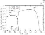
图1是示出了大气环境中的各种电磁辐射波长的透射率的曲线图100。沿着曲线图100的横轴示出电磁辐射波长(以μm为单位),并且沿着曲线图100的纵轴示出透射率(以百分比(%)为单位)。针对特定波长小于100%的透射率意味着大气环境吸收具有特定波长的电磁辐射的至少一部分。FIG. 1 is a
图1中还示出了大气环境102以及大气环境102中的吸收特定波长的电磁辐射(在一些情况下,干扰或抑制预期的感测操作)的一些分子的框图表示。图1所示的分子包括水(H2O)、氧气(O2)和二氧化碳(CO2)。Also shown in FIG. 1 is a block diagram representation of
在一些情况下,检测宽范围的SWIR波长可为有用的。例如,检测包括约1.4μm-1.5μm与约2.5μm之间的SWIR波长的SWIR波长的范围(或多个范围)可为有用的。该范围包括SWIR波长不被吸收(或相反地,透射)的两个窗口。透射SWIR波长的第一窗口或范围从约1.4μm-1.5μm延伸至约1.85μm。透射SWIR波长的第二窗口或范围从约2.0μm延伸至约2.5μm。这些窗口/范围在图1中示出。这两个窗口之间的SWIR波长(即,约1.85μm至约2.0μm的SWIR波长)被水吸收。In some cases, it may be useful to detect a broad range of SWIR wavelengths. For example, it may be useful to detect a range (or ranges) of SWIR wavelengths including SWIR wavelengths between about 1.4 μm-1.5 μm and about 2.5 μm. This range includes two windows where SWIR wavelengths are not absorbed (or conversely, transmitted). A first window or range of transmitted SWIR wavelengths extends from about 1.4 μm-1.5 μm to about 1.85 μm. The second window or range of transmitted SWIR wavelengths extends from about 2.0 μm to about 2.5 μm. These windows/ranges are shown in Figure 1. SWIR wavelengths between these two windows (ie, SWIR wavelengths from about 1.85 μm to about 2.0 μm) are absorbed by water.
InGaAs电磁辐射检测器(以下简称为InGaAs检测器,或简称为检测器)可用于检测在约1.4μm-2.5μm的范围内的SWIR波长,但是至少常规地,单吸收器BSI配置的InGaAs检测器不能以高SNR检测该范围的低端的SWIR波长。为了使用单个检测器来检测更宽范围的SWIR波长内的电磁辐射或为了使用单个检测器来检测不同范围的SWIR波长,需要一种新型的SWIR电磁辐射检测器。尽管FSI配置的InGaAs检测器可检测更大范围的SWIR波长,并且不遭受缓冲吸收,但是浸没式聚光透镜无法形成在FSI配置的InGaAs检测器上。具有浸没式聚光透镜的InGaAs检测器通常将能够通过将接收到的电磁辐射波长集中到比将以其他方式可能的区域更小的区域中来实现更高的SNR。InGaAs electromagnetic radiation detectors (hereinafter referred to simply as InGaAs detectors, or simply detectors) are available for detecting SWIR wavelengths in the range of about 1.4 μm-2.5 μm, but at least conventionally, InGaAs detectors in a single-absorber BSI configuration SWIR wavelengths at the low end of the range cannot be detected with high SNR. To detect electromagnetic radiation over a wider range of SWIR wavelengths using a single detector or to detect different ranges of SWIR wavelengths using a single detector, a new type of SWIR electromagnetic radiation detector is needed. Although the FSI-configured InGaAs detector can detect a wider range of SWIR wavelengths and does not suffer from buffer absorption, an immersion condenser lens cannot be formed on the FSI-configured InGaAs detector. An InGaAs detector with an immersion condenser lens will generally be able to achieve higher SNR by concentrating the received electromagnetic radiation wavelengths into a smaller area than would otherwise be possible.
在一些情况下,本文所述的技术可用于构造可检测在其他光谱范围内的电磁辐射波长的电磁辐射检测器。这些其他范围可包括带SWIR波长、与SWIR波长重叠或与SWIR波长不相交的范围。In some cases, the techniques described herein can be used to construct electromagnetic radiation detectors that can detect electromagnetic radiation wavelengths in other spectral ranges. These other ranges may include ranges with, overlapping with, or disjoint with SWIR wavelengths.
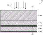
图2A示出了InGaAs检测器200的第一示例。检测器200包括InP基板202,该InP基板具有与第二表面206相对的第一表面204。多个InGaAs电磁辐射吸收器208、210和其他结构(例如,一组一个或多个缓冲层212)可形成在第一表面204上,并且可借助于投射在第二表面206上并且穿过该第二表面的电磁辐射214将电磁辐射214接收到检测器200中。电磁辐射214通过第二表面206的接收以及电磁辐射214在投射于堆叠在第一表面204上的InGaAs电磁辐射吸收器208、210之前通过InP基板202的随后传播使检测器200成为背照式InGaAs检测器。FIG. 2A shows a first example of an
第一InGaAs电磁辐射吸收器208可堆叠在InP基板202的第一表面204上,并且更具体地,可直接在第一表面204上外延生长作为晶格匹配InGaAs层(即,与InP基板晶格匹配的层)。p-n结可在外延生长期间经由植入和/或掺杂形成在第一InGaAs电磁辐射吸收器208中。The first InGaAs
一组一个或多个缓冲层212可堆叠在第一InGaAs电磁辐射吸收器208上。更具体地,并且在一些实施方案中,每个缓冲层可直接在第一InGaAs电磁辐射吸收器208上生长或在缓冲层212中的另一个缓冲层上生长。每个缓冲层可为例如InAsP层,并且每个连续缓冲层可以分级配置生长以使晶格常数从第一InGaAs电磁辐射吸收器208的第一值向第二InGaAs电磁辐射吸收器210的第二值转变。A set of one or more buffer layers 212 may be stacked on the first InGaAs
第二InGaAs电磁辐射吸收器210可堆叠在该一组一个或多个缓冲层212上,并且更具体地,可直接在缓冲层中的一个缓冲层上外延生长。第二InGaAs电磁辐射吸收器210可在缓冲层上生长作为非晶格匹配InGaAs层(即,作为与InP基板202非晶格匹配的层(例如,经扩展或应变的InGaAs层)),但是可具有与其生长所在的缓冲层的晶格常数基本匹配的晶格常数。因此,第二InGaAs电磁辐射吸收器210可经历通常将作为隔离的吸收器而具有的晶格常数环境(以及因此性能)。p-n结可经由植入、利用外延生长期间的掺杂和/或利用扩散掺杂形成在第二InGaAs电磁辐射吸收器210中。p-n结也可形成在InAsP的覆盖层中,而不是形成在InGaAs电磁辐射吸收器210本身中。The second InGaAs
第二InGaAs电磁辐射吸收器210可具有比该一组一个或多个缓冲层212更小的带隙。The second InGaAs
当电磁辐射214投射在InP基板202的第二表面206上时,一些或所有电磁辐射214可穿过InP基板202并且被第一InGaAs电磁辐射吸收器208吸收。例如,第一组电磁辐射波长(例如,第一电磁辐射波长范围)可穿过InP基板202并且被第一InGaAs电磁辐射吸收器208吸收。投射在第一InGaAs电磁辐射吸收器208上的一些电磁辐射214可在不被吸收的情况下或在最小限度的吸收的情况下穿过第一InGaAs电磁辐射吸收器208,并且被该一组一个或多个缓冲层212吸收。被该一组一个或多个缓冲层212吸收的电磁辐射可包括第一组电磁辐射波长中的至少一些电磁辐射波长。被该一组一个或多个缓冲层212吸收的电磁辐射还可包括其他电磁辐射波长。投射在第一InGaAs电磁辐射吸收器208上的一些电磁辐射也可穿过该一组一个或多个缓冲层212并且投射在第二InGaAs电磁辐射吸收器210上。该电磁辐射中的至少一些电磁辐射(例如,第二组电磁辐射波长,诸如第二电磁辐射波长范围)可被第二InGaAs电磁辐射吸收器210吸收。第二组电磁辐射波长可包括不在第一组电磁辐射波长中的至少一些电磁辐射波长,并且在一些情况下,可仅包括不在第一组电磁辐射波长中的电磁辐射波长。第二组电磁辐射波长通常包括比第一组波长更长的波长。When
在一些实施方案中,第一InGaAs电磁辐射吸收器208可被配置为吸收在约1.4μm至约1.7μm的范围内的电磁辐射波长,并且第二InGaAs电磁辐射吸收器210可被配置为吸收在约1.7μm至约2.5μm的范围内的电磁辐射波长。为了本说明书的目的,如果材料或层(诸如电磁辐射吸收器)针对电磁辐射波长具有0.5安培/瓦特(A/W)或更大的响应度(并且优选地,0.6A/W或0.7A/W或更大的响应度),则认为该材料或层“吸收”电磁辐射波长。或在缓冲器或缓冲层的情况下,如果缓冲器或缓冲层以某种任意单位(a.u.)具有等效吸收。同样为了本说明书的目的,“约”特定电磁辐射波长被认为在该特定电磁辐射波长的+/-50纳米(nm)内。In some embodiments, the first InGaAs
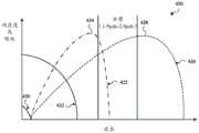
图2B示出了参考图2A描述的InGaAs检测器的吸收器的示例性响应度220。FIG. 2B shows an
第一InGaAs电磁辐射吸收器208具有第一响应度222并且可吸收在第一电磁辐射波长224周围的特定电磁辐射波长范围。The first InGaAs
第二InGaAs电磁辐射吸收器210具有第二响应度226并且可吸收在第二电磁辐射波长228周围的特定电磁辐射波长范围。如图所示,第二InGaAs电磁辐射吸收器210通常可吸收比第一InGaAs电磁辐射吸收器208更长的电磁辐射波长。因为电磁辐射首先投射在第一InGaAs电磁辐射吸收器208上,并且仅在穿过第一InGaAs电磁辐射吸收器208之后投射在第二InGaAs电磁辐射吸收器210上,所以被第一InGaAs电磁辐射吸收器208吸收的电磁辐射波长中的较少电磁辐射波长(或在一些情况下没有电磁辐射波长)可投射在第二InGaAs电磁辐射吸收器210上(并且被该第二InGaAs电磁辐射吸收器吸收)。在其他实施方案中,第一InGaAs电磁辐射吸收器208和第二InGaAs电磁辐射吸收器210的吸收范围可不重叠(例如,它们可不相交)。The second InGaAs
该一组一个或多个缓冲层212与吸收(或缓冲损失)230相关联。一个或多个缓冲层212的吸收范围可与第一InGaAs电磁辐射吸收器208的一些或全部吸收范围重叠,并且在一些情况下可与第二InGaAs电磁辐射吸收器210的一些(但并非全部)吸收范围重叠。因为电磁辐射首先投射在第一InGaAs电磁辐射吸收器208上,并且仅在投射在第一InGaAs电磁辐射吸收器208上之后投射在该一组一个或多个缓冲层212上,所以在第一InGaAs电磁辐射吸收器208的吸收范围内的电磁辐射可在其被该一组一个或多个缓冲层212吸收之前被第一InGaAs电磁辐射吸收器208吸收,从而避免缓冲吸收损失对第一InGaAs电磁辐射吸收器208的影响。另外,该一组一个或多个缓冲层212可吸收可被第一InGaAs电磁辐射吸收器208吸收但不被第一InGaAs电磁辐射吸收器208吸收的一些或所有电磁辐射,使得第二InGaAs电磁辐射吸收器210的响应度被更具体地调谐为不与第一InGaAs电磁辐射吸收器的吸收范围重叠的吸收范围(尽管被第一InGaAs电磁辐射吸收器208和第二InGaAs电磁辐射吸收器210吸收的电磁辐射波长中的一些重叠是可能的并且甚至是可能的)。The set of one or more buffer layers 212 is associated with absorption (or buffer loss) 230 . The absorption range of the one or more buffer layers 212 may overlap with some or all of the absorption range of the first InGaAs
图3A示出了如参考图2A所描述一般构造的InGaAs检测器的一个特定实施方案的示例性响应度300。图3B示出了特定实施方案的示例性检测能力310。如图3A所示,第一InGaAs电磁辐射吸收器208具有在约1.7μm处带有吸收截止的响应度302,并且可具有延伸到低于1.2μm(并且在一些情况下延伸到光谱的开始处)的吸收范围。第二InGaAs电磁辐射吸收器210在具有约1.7μm的吸收接通的情况下具有从约1.4μm延伸到约2.5μm的响应度304。因此,第一InGaAs电磁辐射吸收器208和第二InGaAs电磁辐射吸收器210的响应度302、304在约1.7μm处相交(即,具有交变点)。Figure 3A shows an
该一组一个或多个缓冲层212与吸收(或缓冲损失)306相关联,该吸收(或缓冲损失)与第一InGaAs电磁辐射吸收器的响应度302的一部分重叠。The set of one or more buffer layers 212 is associated with an absorption (or buffer loss) 306 that overlaps a portion of the
如图3B所示,第一InGaAs电磁辐射吸收器208的检测能力312(以琼斯为单位)在约1.7μm以下更高(如在第一InGaAs电磁辐射吸收器208与第二InGaAs电磁辐射吸收器210之间),并且第二InGaAs电磁辐射吸收器210的检测能力314在约1.7μm与2.5μm之间更高。参考图3A和图3B描述的InGaAs检测器的有利之处可在于,该InGaAs检测器的第一InGaAs电磁辐射吸收器与该InGaAs检测器的InP基板晶格匹配,并且不存在可能通过例如增加暗电流而干扰第一InGaAs电磁辐射吸收器的缓冲层,该暗电流可干扰该第一InGaAs电磁辐射吸收器响应于该第一InGaAs电磁辐射吸收器在其吸收范围内的电磁辐射的吸收而生成的电流的读出。另外,较短波长(即,较大带隙)半导体通常具有低暗电流密度。As shown in FIG. 3B , the detection capability 312 (in Jones) of the first InGaAs
在一些情况下,可能希望调整吸收器对作出响应的电磁辐射波长范围(即,吸收器吸收的电磁辐射波长范围)。在一些情况下,可通过调整一个或多个缓冲层的数量或厚度来调整更远离InP基板的InGaAs电磁辐射吸收器的响应度,该一个或多个缓冲层将该InP基板与在电磁辐射传播路径中较早定位的InGaAs电磁辐射吸收器分离。在一些情况下,可通过用一组附加的一个或多个缓冲层将最接近InP基板定位的InGaAs电磁辐射吸收器与InP基板分离来调整该InGaAs电磁辐射吸收器的响应度,如下文参考例如图4A和图4B所描述。在一些情况下,可通过改变InGaAs电磁辐射吸收器的组成或生长方法和/或通过调整将该InGaAs电磁辐射吸收器与InP基板或其他InGaAs电磁辐射吸收器分离的缓冲层的数量、厚度或类型来调整该InGaAs电磁辐射吸收器的响应度。In some cases, it may be desirable to adjust the wavelength range of electromagnetic radiation to which the absorber responds (ie, the wavelength range of electromagnetic radiation absorbed by the absorber). In some cases, the responsivity of the InGaAs electromagnetic radiation absorber further away from the InP substrate can be tuned by adjusting the number or thickness of one or more buffer layers that separate the InP substrate from the electromagnetic radiation transmitted by the InP substrate. The InGaAs electromagnetic radiation absorber positioned earlier in the path separates. In some cases, the responsivity of an InGaAs electromagnetic radiation absorber positioned proximate to the InP substrate can be adjusted by separating the InGaAs electromagnetic radiation absorber from the InP substrate with an additional set of one or more buffer layers, as referenced below for example Figure 4A and Figure 4B are described. In some cases, the InGaAs electromagnetic radiation absorber can be changed by changing the composition or growth method of the InGaAs electromagnetic radiation absorber and/or by adjusting the number, thickness or type of buffer layer separating the InGaAs electromagnetic radiation absorber from the InP substrate or other InGaAs electromagnetic radiation absorber. to adjust the responsivity of the InGaAs electromagnetic radiation absorber.
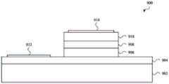
图4A示出了InGaAs检测器400的第二示例。检测器400包括InP基板402,该InP基板具有与第二表面406相对的第一表面404。多个InGaAs电磁辐射吸收器408、410和其他结构(例如,一组或多组缓冲层412、414)可形成在第一表面404上,并且可借助于投射在第二表面406上并且穿过该第二表面的电磁辐射416将电磁辐射416接收到检测器400中。电磁辐射416通过第二表面406的接收以及电磁辐射416在投射于堆叠在第一表面404上的InGaAs电磁辐射吸收器408、410之前通过InP基板402的随后传播使检测器400成为背照式InGaAs检测器。A second example of an
第一组一个或多个缓冲层412可堆叠在InP基板402的第一表面404上。更具体地,并且在一些实施方案中,第一组中的每个缓冲层可直接在InP基板402上外延生长或在缓冲层412中的另一个缓冲层上外延生长。每个缓冲层可为例如InAsP层,并且每个连续缓冲层可以分级配置生长以使晶格常数从InP基板402的第一值向第一InGaAs电磁辐射吸收器408的第二值转变。A first set of one or more buffer layers 412 may be stacked on the
第一InGaAs电磁辐射吸收器408可堆叠在第一组一个或多个缓冲层412上,其中缓冲层412设置在InP基板402与第一InGaAs电磁辐射吸收器408之间。更具体地,并且在一些实施方案中,第一InGaAs电磁辐射吸收器408可直接在第一组一个或多个缓冲层412中的缓冲层上外延生长作为短的晶格失配InGaAs层(即,作为与InP基板晶格失配的层),但是可具有与其生长所在的缓冲层的晶格常数基本匹配的晶格常数。因此,第一InGaAs电磁辐射吸收器408可经历通常将作为隔离的吸收器而具有的晶格常数环境(以及因此性能)。p-n结可经由植入、利用外延生长期间的掺杂和/或利用扩散掺杂形成在第一InGaAs电磁辐射吸收器408中。p-n结也可形成在InAsP的覆盖层中,而不是形成在InGaAs电磁辐射吸收器410本身中。The first InGaAs
第二组一个或多个缓冲层414可堆叠在第一InGaAs电磁辐射吸收器408上。更具体地,并且在一些实施方案中,该组中的每个缓冲层可直接在第一InGaAs电磁辐射吸收器408上外延生长或在缓冲层414中的另一个缓冲层上外延生长。每个缓冲层可为例如InAsP层,并且每个连续缓冲层可以分级配置生长以使晶格常数从第一InGaAs电磁辐射吸收器408的第一值向第二InGaAs电磁辐射吸收器410的第二值转变。A second set of one or more buffer layers 414 may be stacked on the first InGaAs
第二InGaAs电磁辐射吸收器410可堆叠在第二组一个或多个缓冲层414上,其中缓冲层414设置在第一InGaAs电磁辐射吸收器408与第二InGaAs电磁辐射吸收器410之间。更具体地,并且在一些实施方案中,第二InGaAs电磁辐射吸收器410可在第二组一个或多个缓冲层414中的缓冲层上外延生长作为长的或延伸的晶格失配InGaAs层(即,作为与InP基板402非晶格匹配的层(例如,经延伸或应变的InGaAs层)),但是可具有与其生长所在的缓冲层的晶格常数基本匹配的晶格常数。因此,第二InGaAs电磁辐射吸收器410可经历通常将作为隔离的吸收器而具有的晶格常数环境(以及因此性能)。p-n结可经由植入、利用外延生长期间的掺杂和/或利用扩散掺杂形成在第二InGaAs电磁辐射吸收器410中。p-n结也可形成在InAsP的覆盖层中,而不是形成在InGaAs电磁辐射吸收器410本身中。The second InGaAs
第一InGaAs电磁辐射吸收器408可具有比第一组一个或多个缓冲层412更大的带隙。类似地,第二InGaAs电磁辐射吸收器410可具有比第二组一个或多个缓冲层414更大的带隙。这使得每个InGaAs电磁辐射吸收器408、410能够吸收被更接近InP基板402的层吸收的更长的电磁辐射波长。The first InGaAs
当电磁辐射416投射在InP基板402的第二表面406上时,一些或所有电磁辐射416可穿过InP基板402并且被第一InGaAs电磁辐射吸收器408吸收。例如,第一组电磁辐射波长(例如,第一电磁辐射波长范围)可穿过InP基板402并且被第一InGaAs电磁辐射吸收器408吸收。被第一InGaAs电磁辐射吸收器408吸收的该组电磁辐射波长可受到第一组一个或多个缓冲层412的吸收范围的影响。例如,被第一组缓冲层412吸收的电磁辐射波长将不会投射在第一InGaAs电磁辐射吸收器408上。在一些情况下,第一组一个或多个缓冲层412可用于调整(或调谐)被第一InGaAs电磁辐射吸收器408吸收的电磁辐射波长范围的一个或两个界限。When
投射在第一InGaAs电磁辐射吸收器408上的一些电磁辐射416可在不被吸收的情况下或在最小限度的吸收的情况下穿过第一InGaAs电磁辐射吸收器408,并且被第二组一个或多个缓冲层414吸收。由第二组一个或多个缓冲层414吸收的电磁辐射可包括第一组电磁辐射波长中的至少一些电磁辐射波长。由第二组一个或多个缓冲层414吸收的电磁辐射还可包括其他电磁辐射波长。投射在第一InGaAs电磁辐射吸收器408上的一些电磁辐射也可穿过第二组一个或多个缓冲层414并且投射在第二InGaAs电磁辐射吸收器410上。该电磁辐射中的至少一些电磁辐射(例如,第二组电磁辐射波长,诸如第二电磁辐射波长范围)可被第二InGaAs电磁辐射吸收器410吸收。第二组电磁辐射波长可包括不在第一组电磁辐射波长中的至少一些电磁辐射波长,并且在一些情况下,可仅包括不在第一组电磁辐射波长中的电磁辐射波长。第二组电磁辐射波长通常包括比第一组波长更长的波长。Some of the
在一些实施方案中,第一InGaAs电磁辐射吸收器408可被配置为吸收在约1.4μm至约1.9μm或2.0μm的范围内的电磁辐射波长,并且第二InGaAs电磁辐射吸收器410可被配置为吸收在约1.9μm或2.0μm至约2.5μm的范围内的电磁辐射波长。将第一InGaAs电磁辐射检测器的吸收范围的截止配置在约1.85μm至约2.0μm的范围内(即,电磁辐射主要被水吸收的带,如参考图1所讨论的)并且将第二InGaAs电磁辐射检测器的吸收范围的接通配置在相同范围内将吸收器响应度之间的交变置于可执行不太有用的感测(至少在一些应用程序中)的电磁辐射波长范围内。In some embodiments, the first InGaAs
图4B示出了参考图4A描述的InGaAs检测器的吸收器的示例性响应度420。FIG. 4B shows an
第一InGaAs电磁辐射吸收器408具有第一响应度422并且可吸收在第一电磁辐射波长424周围的特定电磁辐射波长范围。The first InGaAs
第二InGaAs电磁辐射吸收器410具有第二响应度426并且可吸收在第二电磁辐射波长428周围的特定电磁辐射波长范围。如图所示,第二InGaAs电磁辐射吸收器410通常可吸收比第一InGaAs电磁辐射体408更长的电磁辐射波长。因为电磁辐射首先投射在第一InGaAs电磁辐射吸收器408上,并且仅在穿过第一InGaAs电磁辐射吸收器408之后投射在第二InGaAs电磁辐射吸收器410上,所以被第一InGaAs电磁辐射吸收器408吸收的电磁辐射波长中的较少电磁辐射波长(或在一些情况下没有电磁辐射波长)可投射在第二InGaAs电磁辐射吸收器410上(并且被该第二InGaAs电磁辐射吸收器吸收)。在其他实施方案中,第一InGaAs电磁辐射吸收器408和第二InGaAs电磁辐射吸收器410的吸收范围可不重叠(例如,它们可不相交)。The second InGaAs
第一组一个或多个缓冲层412与吸收(或缓冲损失)430相关联。第一组一个或多个缓冲层412的吸收范围可忽略不计,并且通常可在第一InGaAs电磁辐射吸收器408和第二InGaAs电磁辐射吸收器410的吸收范围之外。The first set of one or more buffer layers 412 is associated with absorption (or buffer loss) 430 . The absorption range of the first set of one or more buffer layers 412 is negligible and may generally be outside the absorption range of the first InGaAs
第二组一个或多个缓冲层414与吸收(或缓冲损失)432相关联。第二组一个或多个缓冲层414的吸收范围可与第一InGaAs电磁辐射吸收器408的一些或全部吸收范围重叠,并且在一些情况下可与第二InGaAs电磁辐射吸收器410的一些(但并非全部)吸收范围重叠。因为电磁辐射首先投射在第一InGaAs电磁辐射吸收器408上,并且仅在投射在第一InGaAs电磁辐射吸收器408上之后投射在第二组一个或多个缓冲层414上,所以在第一InGaAs电磁辐射吸收器408的吸收范围内的电磁辐射可在其被第二组一个或多个缓冲层414吸收之前被第一InGaAs电磁辐射吸收器408吸收,从而避免缓冲吸收损失对第一InGaAs电磁辐射吸收器408的影响。另外,第二组一个或多个缓冲层414可吸收可被第一InGaAs电磁辐射吸收器408吸收但不被第一InGaAs电磁辐射吸收器408吸收的一些或所有电磁辐射,使得第二InGaAs电磁辐射吸收器410的响应度被更具体地调谐为不与第一InGaAs电磁辐射吸收器的吸收范围重叠的吸收范围(尽管被第一InGaAs电磁辐射吸收器408和第二InGaAs电磁辐射吸收器410吸收的电磁辐射波长中的一些重叠是可能的并且甚至是可能的)。The second set of one or more buffer layers 414 is associated with absorption (or buffer loss) 432 . The absorption range of the second set of one or more buffer layers 414 may overlap with some or all of the absorption range of the first InGaAs
图5A示出了如参考图4A所描述一般构造的InGaAs检测器的一个特定实施方案的示例性响应度500。图5B示出了特定实施方案的示例性检测能力510。Figure 5A shows an
如图5A所示,第一InGaAs电磁辐射吸收器408具有在约1.9μm处带有吸收截止的响应度502,并且可具有延伸到约1.2μm的吸收范围。第二InGaAs电磁辐射吸收器410在具有约1.9μm的吸收接通的情况下具有从约1.4μm延伸到约2.5μm的响应度504。因此,第一InGaAs电磁辐射吸收器408和第二InGaAs电磁辐射吸收器410的响应度502、504在约1.9μm处相交(即,具有交变点)。As shown in FIG. 5A, the first InGaAs
第一组一个或多个缓冲层412与通常在第一InGaAs电磁辐射检测器408和第二InGaAs电磁辐射检测器410的响应度之外的吸收(或缓冲损失)506相关联,并且第二组一个或多个缓冲层414与同第一InGaAs电磁辐射吸收器响应度502和第二InGaAs电磁辐射吸收器响应度504的部分重叠的吸收(或缓冲损失)508相关联。The first set of one or more buffer layers 412 is associated with absorption (or buffer loss) 506 that is generally outside the responsivity of the first InGaAs
如图5B所示,第一InGaAs电磁辐射吸收器408的检测能力512(以琼斯为单位)在约1.2μm与1.9μm之间更高(如在第一InGaAs电磁辐射吸收器408与第二InGaAs电磁辐射吸收器410之间),并且第二InGaAs电磁辐射吸收器410的检测能力514在约1.9μm与2.5μm之间更高。As shown in FIG. 5B, the detection capability 512 (in Jones) of the first InGaAs
参考图5A和图5B描述的InGaAs检测器的有利之处可在于,该InGaAs检测器的第一InGaAs电磁辐射吸收器与第二InGaAs电磁辐射吸收器之间的交变点在水分吸收带(例如,在约1.85μm与约2.0μm之间的水分吸收带,如参考图1描述的)内。换句话讲,交变点处于可进行不太有用的感测的电磁辐射波长(或波长范围)处。An advantage of the InGaAs detector described with reference to FIGS. 5A and 5B may be that the transition point between the first InGaAs electromagnetic radiation absorber and the second InGaAs electromagnetic radiation absorber of the InGaAs detector is within the moisture absorption band (e.g. , within the moisture absorption band between about 1.85 μm and about 2.0 μm, as described with reference to FIG. 1 ). In other words, the transition point is at a wavelength (or range of wavelengths) of electromagnetic radiation where less useful sensing is possible.
图6A示出了如参考图4A所描述一般构造的InGaAs检测器的另一特定实施方案的示例性响应度600。图6B示出了特定实施方案的示例性检测能力610。Figure 6A shows an
如图6A所示,第一InGaAs电磁辐射吸收器408具有在约2.1μm处带有吸收截止的响应度602,并且可具有延伸到约1.4μm的吸收范围。第二InGaAs电磁辐射吸收器410在具有约2.1μm的吸收接通的情况下具有从约1.6μm延伸到约2.5μm的响应度604。因此,第一InGaAs电磁辐射吸收器408和第二InGaAs电磁辐射吸收器410的响应度602、604在约2.1μm处相交(即,具有交变点)。As shown in FIG. 6A, the first InGaAs
第一组一个或多个缓冲层412与同第一InGaAs电磁辐射检测器408的响应度的一部分重叠的吸收(或缓冲损失)606相关联,并且第二组一个或多个缓冲层414与同第一InGaAs电磁辐射吸收器响应度602和第二InGaAs电磁辐射吸收器响应度604的部分重叠的吸收(或缓冲损失)608相关联。The first set of one or more buffer layers 412 is associated with absorption (or buffer loss) 606 that overlaps with a portion of the responsivity of the first InGaAs
如图6B所示,第一InGaAs电磁辐射吸收器408的检测能力612(以琼斯为单位)在约1.4μm与2.1μm之间更高(如在第一InGaAs电磁辐射吸收器408与第二InGaAs电磁辐射吸收器410之间),并且第二InGaAs电磁辐射吸收器410的检测能力614在约2.1μm与2.5μm之间更高。As shown in FIG. 6B, the detection capability 612 (in Jones) of the first InGaAs
参考图6A和图6B描述的InGaAs检测器的有利之处可在于,该InGaAs检测器的第一InGaAs电磁辐射吸收器在比本文所述的其他InGaAs检测器更长的电磁辐射波长处具有截止。当电磁辐射穿过例如以到达第一InGaAs电磁辐射吸收器的缓冲层不吸收感兴趣范围内的电磁辐射波长时(例如,当缓冲层仅吸收低于1.4μm的电磁辐射波长时),可存在较少暗电流,该暗电流干扰该第一InGaAs电磁辐射吸收器响应于该第一InGaAs电磁辐射吸收器在其吸收范围内的电磁辐射的吸收而生成的电流的读出。对更接近InP基板的缓冲层的吸收范围的以上限制可对缓冲层的组成(例如,InAsP组成)施加约束,并且因此对可得到的晶格常数施加约束,并且因此对第一电磁辐射吸收器的组成(例如,InGaAs组成)施加约束,并且因此对第一电磁辐射吸收器的长波长截止施加约束。这种设计确保在任何感兴趣波长处,没有吸收器的响应度被缓冲吸收降低。The InGaAs detector described with reference to FIGS. 6A and 6B may be advantageous in that the first InGaAs electromagnetic radiation absorber of the InGaAs detector has a cutoff at a longer wavelength of electromagnetic radiation than other InGaAs detectors described herein. When the buffer layer through which the electromagnetic radiation passes, for example to reach the first InGaAs electromagnetic radiation absorber, does not absorb electromagnetic radiation wavelengths in the range of interest (e.g., when the buffer layer only absorbs electromagnetic radiation wavelengths below 1.4 μm), there may be Less dark current that interferes with the readout of the current generated by the first InGaAs electromagnetic radiation absorber in response to absorption of electromagnetic radiation by the first InGaAs electromagnetic radiation absorber within its absorption range. The above limitation on the absorption range of the buffer layer closer to the InP substrate may impose constraints on the composition of the buffer layer (e.g., InAsP composition), and thus on the available lattice constants, and thus on the first electromagnetic radiation absorber The composition (for example, InGaAs composition) of , and thus the long-wavelength cutoff of the first electromagnetic radiation absorber, imposes constraints. This design ensures that at any wavelength of interest, the responsivity of no absorber is reduced by buffer absorption.
在一些实施方案中,如参考图2A或图4A所描述一般构造的InGaAs检测器可包括堆叠在一组或多组附加的一个或多个缓冲层上的一个或多个附加InGaAs电磁辐射吸收器。例如,InGaAs检测器可包括堆叠在第三组一个或多个缓冲层上的第三InGaAs电磁辐射吸收器,该第三组一个或多个缓冲层可堆叠在检测器的第二InGaAs电磁辐射吸收器上。In some embodiments, an InGaAs detector generally constructed as described with reference to FIG. 2A or FIG. 4A may include one or more additional InGaAs electromagnetic radiation absorbers stacked on one or more additional sets of one or more buffer layers . For example, an InGaAs detector may include a third InGaAs electromagnetic radiation absorber stacked on a third set of one or more buffer layers, which may be stacked on a second InGaAs electromagnetic radiation absorbing absorber of the detector. device.
在一些实施方案中,检测器可包括基板、缓冲层和/或带有其他材料的电磁辐射吸收器。例如,基板可由砷化镓(GaAs)、碲化镉(CdTe)或硅(Si)形成。在GaAs、CdTe或Si基板的情况下,电磁辐射吸收器在一些情况下可由碲化汞镉(HgCdTe)形成。In some embodiments, a detector may include a substrate, a buffer layer, and/or an electromagnetic radiation absorber with other materials. For example, the substrate may be formed of gallium arsenide (GaAs), cadmium telluride (CdTe), or silicon (Si). In the case of GaAs, CdTe or Si substrates, the electromagnetic radiation absorber may in some cases be formed from mercury cadmium telluride (HgCdTe).
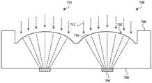
图7A示出了具有浸没式聚光透镜702的背照式InGaAs检测器700的示例性使用。在一些示例中,InGaAs检测器700可包括参考图2A至图6B中的一个或多个图描述的InGaAs电磁辐射吸收器和缓冲层。FIG. 7A shows an exemplary use of a back-illuminated
InGaAs检测器700可具有多个InGaAs电磁辐射吸收器(即,两个或更多个InGaAs电磁辐射吸收器)以及堆叠(例如,生长)在InP基板708的第一表面706上的一组或多组一个或多个缓冲层,这些缓冲层共同标记为704。InP基板708可具有第二表面710,在该第二表面上形成(例如,蚀刻)浸没式聚光透镜702,使得InGaAs电磁辐射吸收器和缓冲层704浸没在连续高折射率介质(即,InP基板708)中。浸没式聚光透镜702可改善电磁辐射712通过InGaAs检测器700的InP基板708的传送。The
浸没式聚光透镜702可通过InP基板708的第二表面710(其可为凸形表面)接收电磁辐射712,并且将电磁辐射聚焦到InGaAs电磁辐射吸收器和缓冲层704上。Immersion condenser lens 702 may receive electromagnetic radiation 712 through
在一些情况下,InGaAs检测器700可用作单个(例如,独立的)检测器单元。在其他情况下,InGaAs检测器700可为InGaAs检测器700、714或检测器单元的阵列(例如,一维或二维阵列)中的一个检测器单元。例如,不同的InGaAs检测器700、714可共享共用InP基板708(如图所示)和/或其他部件,或可单独制造(或共同制造,并且随后进行切割)并且安装在载体基板上或壳体内。In some cases,
在一些情况下,并且如图7B所示,InGaAs检测器700可用作检测器单元并且定位在发射器单元附近。发射器单元可包括电磁辐射发射器716,该电磁辐射发射器堆叠在透镜720的表面718上或定位在该表面附近,并且被配置为通过透镜720发射电磁辐射。举例来说,透镜720可准直、扩散或聚焦由电磁辐射发射器716发射的电磁辐射。电磁辐射发射器716可发射在可被InGaAs检测器700吸收的电磁辐射范围内、遍及该电磁辐射范围或包括该电磁辐射范围的电磁辐射。在一些实施方案中,可以不设置透镜720。In some cases, and as shown in Figure 7B, an
图8A至图11示出了InGaAs检测器的各种示例性触点布置。举例来说,示出了用于与参考图4描述的InGaAs检测器类似的InGaAs检测器的触点布置。然而,各种触点布置可用于本文所述的任何InGaAs检测器。8A-11 illustrate various exemplary contact arrangements for InGaAs detectors. As an example, a contact arrangement for an InGaAs detector similar to that described with reference to FIG. 4 is shown. However, various contact arrangements can be used with any of the InGaAs detectors described herein.
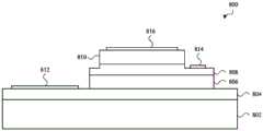
图8A示出了3触点InGaAs检测器800的平面图,并且图8B示出了InGaAs检测器800的立剖面图。InGaAs检测器800包括InP基板802,可选的第一组一个或多个缓冲层(统称为第一缓冲器804)堆叠在该InP基板上。第一InGaAs电磁辐射吸收器806堆叠在第一缓冲器804上(即,其中第一缓冲器804设置在InP基板802与第一InGaAs电磁辐射吸收器806之间),或在不设置第一缓冲器804时堆叠在InP基板802上。第二组一个或多个缓冲层(统称为第二缓冲器808)堆叠在第一InGaAs电磁辐射吸收器806上,并且第二InGaAs电磁辐射吸收器810堆叠在第二缓冲器808上(即,其中第二缓冲器808设置在第一InGaAs电磁辐射吸收器806与第二InGaAs电磁辐射吸收器810之间)。FIG. 8A shows a plan view of a 3-
第一InGaAs电磁辐射吸收器可电气设置在第一电触点812与第二电触点814之间,其中第一电触点812和第二电触点814用于使第一InGaAs电磁辐射吸收器806电气偏置并且感测由第一InGaAs电磁辐射吸收器806生成的第一电流。在一些实施方案中,第一电触点812可沉积于第一缓冲器804上,并且第二电触点814可沉积于第二缓冲器808上。在其他实施方案中,第一电触点812可沉积于例如InP基板802上,或第二电触点814可沉积于第一InGaAs电磁辐射吸收器806上。The first InGaAs electromagnetic radiation absorber can be electrically arranged between the first
第二InGaAs电磁辐射吸收器可电气设置在第二电触点814与第三电触点816之间,其中第二电触点814和第三电触点816用于使第二InGaAs电磁辐射吸收器810电气偏置并且感测由第二InGaAs电磁辐射吸收器810生成的第二电流。在一些实施方案中,第三电触点816可沉积于第二InGaAs电磁辐射吸收器810上。The second InGaAs electromagnetic radiation absorber can be electrically disposed between the second
如图8A所示,第一缓冲器804可在整个InP基板802上方延伸,或在InP基板802的比第一InGaAs电磁辐射吸收器806和第二InGaAs电磁辐射吸收器810以及第二缓冲器808中的每一者更大的部分上方延伸。第一电触点812被示出为沿着第一InGaAs电磁辐射吸收器806的三个侧面延伸,但是在其他实施方案中,可被定位成仅邻近于第一InGaAs电磁辐射吸收器806的一个侧面,或可围绕第一InGaAs电磁辐射吸收器806或具有其他配置。尽管所有基板、缓冲器和吸收器部件的周边在图8A中被示出为矩形或正方形,但是这些元件的周边可另选地具有任何形状。As shown in FIG. 8A, the
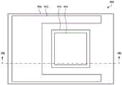
图9A示出了2触点InGaAs检测器900的平面图,并且图9B示出了InGaAs检测器900的立剖面图。InGaAs检测器900包括InP基板902,可选的第一组一个或多个缓冲层(统称为第一缓冲器904)堆叠在该InP基板上。第一InGaAs电磁辐射吸收器906堆叠在第一缓冲器904上(即,其中第一缓冲器904设置在InP基板902与第一InGaAs电磁辐射吸收器906之间),或在不设置第一缓冲器904时堆叠在InP基板902上。第二组一个或多个缓冲层(统称为第二缓冲器908)堆叠在第一InGaAs电磁辐射吸收器906上,并且第二InGaAs电磁辐射吸收器910堆叠在第二缓冲器908上(即,其中第二缓冲器908设置在第一InGaAs电磁辐射吸收器906与第二InGaAs电磁辐射吸收器910之间)。FIG. 9A shows a plan view of a 2-
第一InGaAs电磁辐射吸收器906和第二InGaAs电磁辐射吸收器910可电气设置在第一电触点912与第二电触点914之间,其中第一电触点912和第二电触点914用于使第一InGaAs电磁辐射吸收器906在正向上电气偏置并且感测与由第一InGaAs电磁辐射吸收器906生成的总电流对应的电流。另选地,第一电触点912和第二电触点914可用于使第二InGaAs电磁辐射吸收器910在反向上电气偏置并且感测与由第二InGaAs电磁辐射吸收器910生成的总电流对应的电流。在其他实施方案中,并且取决于第一InGaAs电磁辐射吸收器906和第二InGaAs电磁辐射吸收器910的植入或掺杂,电触点912、914可用于在相反方向上使第一InGaAs电磁辐射吸收器906和第二InGaAs电磁辐射吸收器910偏置和读取该第一InGaAs电磁辐射吸收器和该第二InGaAs电磁辐射吸收器。在一些实施方案中,第一电触点912可沉积于第一缓冲器904上,并且第二电触点914可沉积于第二InGaAs电磁辐射吸收器910上。The first InGaAs
如图9A所示,第一缓冲器904可在整个InP基板902上方延伸,或在InP基板902的比第一InGaAs电磁辐射吸收器906和第二InGaAs电磁辐射吸收器910以及第二缓冲器908中的每一者更大的部分上方延伸。第一电触点912被示出为沿着第一InGaAs电磁辐射吸收器906的三个侧面延伸,但是在其他实施方案中,可被定位成仅邻近于第一InGaAs电磁辐射吸收器906的一个侧面,或可围绕第一InGaAs电磁辐射吸收器906或具有其他配置。尽管所有基板、缓冲器和吸收器部件的周边在图9A中被示出为矩形或正方形,但是这些元件的周边可另选地具有任何形状。As shown in FIG. 9A, the
图10示出了第一InGaAs电磁辐射吸收器1006和第二InGaAs电磁辐射吸收器1010被配置为背对背光电二极管的InGaAs检测器1000的立视图。InGaAs检测器1000包括InP基板1002,第一组一个或多个缓冲层(统称为第一缓冲器1004)堆叠在该InP基板上。第一InGaAs电磁辐射吸收器1006堆叠在第一缓冲器1004上(即,其中第一缓冲器1004设置在InP基板1002与第一InGaAs电磁辐射吸收器1006之间)。第二组一个或多个缓冲层(统称为第二缓冲器1008)堆叠在第一InGaAs电磁辐射吸收器1006上,并且第二InGaAs电磁辐射吸收器1010堆叠在第二缓冲器1008上(即,其中第二缓冲器1008设置在第一InGaAs电磁辐射吸收器1006与第二InGaAs电磁辐射吸收器1010之间)。覆盖层1012堆叠在第二InGaAs电磁辐射吸收器1010上(即,其中第二InGaAs电磁辐射吸收器1010设置在第二缓冲器1008与覆盖层1012之间)。10 shows an elevational view of an
第一InGaAs电磁辐射吸收器1006和第二InGaAs电磁辐射吸收器1010中的每一者可为n掺杂(或n型)InGaAs电磁辐射吸收器。第一缓冲器1004和第二缓冲器1008中的每一者可包括一个或多个磷化铟砷(InAsP)层,其中第一缓冲器1004包括一个或多个p掺杂(或p型)InAsP层,并且其中第二缓冲器1008包括一个或多个n掺杂(或n型)InAsP层。InGaAs电磁辐射吸收器1006、1010、缓冲器1004、1008和覆盖层1012因此形成包括背对背光电二极管的pnnp层结构。施加到pnnp层结构的正向偏置(或另选地,反向偏置)使得能够读出第一InGaAs电磁辐射吸收器1006(或第二InGaAs电磁辐射吸收器1010)。Each of the first InGaAs
在另选的实施方案中,InGaAs电磁辐射吸收器1006、1010、缓冲层1004、1008和覆盖层1012可被植入或掺杂以形成包括背对背光电二极管的nppn、nBn或pBp层结构。In alternative embodiments, the InGaAs
图11示出了第一InGaAs电磁辐射吸收器1106和第二InGaAs电磁辐射吸收器1110被配置为面向相同方向并且通过隧道结连接的两个光电探测器的InGaAs检测器1100的立视图。InGaAs检测器1100包括InP基板1102,第一组一个或多个缓冲层(统称为第一缓冲器1104)堆叠在该InP基板上。第一InGaAs电磁辐射吸收器1106堆叠在第一缓冲器1104上(即,其中第一缓冲器1104设置在InP基板1102与第一InGaAs电磁辐射吸收器1106之间)。第二组一个或多个缓冲层(统称为第二缓冲器1108)堆叠在第一InGaAs电磁辐射吸收器1106上,并且第二InGaAs电磁辐射吸收器1110堆叠在第二缓冲器1108上(即,其中第二缓冲器1108设置在第一InGaAs电磁辐射吸收器1106与第二InGaAs电磁辐射吸收器1110之间)。覆盖层1112堆叠在第二InGaAs电磁辐射吸收器1110上(即,其中第二InGaAs电磁辐射吸收器1110设置在第二缓冲器1108与覆盖层1112之间)。Fig. 11 shows an elevational view of an
第一InGaAs电磁辐射吸收器1106和第二InGaAs电磁辐射吸收器1110中的每一者可为n掺杂(或n型)InGaAs电磁辐射吸收器。第一缓冲器1104和第二缓冲器1108中的每一者可包括一个或多个磷化铟砷(InAsP)层,其中第一缓冲器1104包括一个或多个n掺杂(或n型)InAsP层,并且其中第二缓冲器1108包括一个或多个n掺杂(或n型)InAsP层和一个或多个p掺杂(或p型)InAsP层。InGaAs电磁辐射吸收器1106、1110、缓冲器1104、1108和覆盖层1112因此形成包括具有隧道结的堆叠式光电二极管的pnpn层结构。不同于参考图10描述的InGaAs检测器,隧道结允许以相同的偏置极性从两个InGaAs电磁辐射吸收器1106、1110读出光电流,这需要不同的偏置电压来从不同的InGaAs电磁辐射吸收器提取光电流。Each of the first InGaAs
图12A和图12B示出了包括一组传感器的设备1200(电子设备)的示例。传感器可用于例如从设备1200的穿戴者或用户获取生物信息(例如,心率、呼吸率、血压、血液流速、血液充氧、血糖水平等),或确定设备1200的状态(例如,设备1200是否正在被佩戴或设备1200的紧密度)。设备的尺寸和形状因数以及带1204(例如,腕带)的包括表明设备1200是电子手表、健身监测器或健康诊断设备。然而,设备1200另选地可为任何类型的可穿戴设备。图12A示出了设备1200的前等轴视图,并且图12B示出了设备1200的后等轴视图。12A and 12B illustrate an example of a device 1200 (electronic device) including a set of sensors. Sensors may be used, for example, to obtain biological information (e.g., heart rate, respiration rate, blood pressure, blood flow rate, blood oxygenation, blood glucose levels, etc.) from the wearer or user of
设备1200可包括主体1202(例如,手表主体)和带1204。主体1202可包括输入或选择设备,诸如冠部1218或按钮1220。带1204可附接到主体1202的壳体1206,并且可用于将主体1202附接到用户的身体部位(例如,臂、手腕、腿部、脚踝或腰部)。主体1202可包括至少部分地围绕显示器1208的壳体1206。在一些实施方案中,壳体1206可包括侧壁1210,该侧壁1210可支撑前盖1212(图12A)和/或后盖1214(图12B)。前盖1212可定位在显示器1208上方,并且可提供窗口,通过该窗口可观看显示器1208。在一些实施方案中,显示器1208可附接到(或邻接)侧壁1210和/或前盖1212。在设备1200的另选的实施方案中,可不包括显示器1208和/或壳体1206可具有另选的配置。
显示器1208可包括一个或多个发光元件,包括例如限定发光二极管(LED)显示器、有机LED(OLED)显示器、液晶显示器(LCD)、电致发光(EL)显示器或其他类型的显示器的发光元件。在一些实施方案中,显示器1208可包括一个或多个触摸传感器和/或力传感器,或与之相关联,该触摸传感器和/或力传感器被配置为检测施加到前盖1212的表面的触摸和/或力。
在一些实施方案中,壳体1206的侧壁1210可使用一种或多种金属(例如,铝或不锈钢)、聚合物(例如,塑料)、陶瓷或复合材料(例如,碳纤维)形成。可例如使用玻璃、晶体(例如,蓝宝石)或透明聚合物(例如,塑料)中的一者或多者来形成前盖1212,该玻璃、晶体或透明聚合物使得用户能够通过前盖1212观看显示器1208。在一些情况下,前盖1212的一部分(例如,前盖1212的周边部分)可涂覆有不透明油墨,以遮盖壳体1206内所包括的部件。在一些情况下,壳体1206的所有外部部件可由透明材料形成,并且设备1200内的部件可被壳体1206内的不透明油墨或不透明结构遮盖或不遮盖。In some embodiments,
后盖1214可使用与用于形成侧壁1210或前盖1212的材料相同的材料形成。在一些情况下,后盖1214可为也形成侧壁1210的整体式元件的一部分。在其他情况下,并且如图所示,后盖1214可为多部分后盖,诸如具有附接到侧壁1210的第一后盖部分1214-1和附接到第一后盖部分1214-1的第二后盖部分1214-2的后盖。在一些情况下,第二后盖部分1214-2可具有圆形周边和弓形外表面1216(即,具有弓形轮廓的外表面1216)。The
可使用紧固件、粘合剂、密封件、垫圈或其他部件将前盖1212、后盖1214或第一后盖部分1214-1安装到侧壁1210。当存在时,可使用紧固件、粘合剂、密封件、垫圈或其他部件将第二后盖部分1214-2安装到第一后盖部分1214-1。
包括显示器1208的显示器叠层或设备叠层(以下称为“叠层”)可附接(或邻接)到前盖1212的内表面并且延伸到设备1200的内部体积中。在一些情况下,叠层可以包括触摸传感器(例如,电容、电阻、基于应变的、超声或其他类型的触摸感测元件的网格)或光学、机械、电气或其他类型的部件的其他层。在一些情况下,触摸传感器(或触摸传感器系统的一部分)可被配置为检测施加到前盖1212的外表面(例如,施加到设备1200的显示表面)的触摸。A display stack or device stack (hereinafter “stack”) including
在一些情况下,力传感器(或力传感器系统的一部分)可定位在显示器1208下方和/或侧面的内部体积内(并且在一些情况下,定位在设备叠层内)。力传感器(或力传感器系统)可响应于触摸传感器检测到前盖1212上的一个或多个触摸(或前盖1212上一个或多个触摸的一个或多个位置)而被触发,并且可确定与每个触摸相关联的力的大小,或与整个触摸集合相关联的力的大小。力传感器(或力传感器系统)可另选地触发触摸传感器(或触摸传感器系统)的操作,或者可独立于触摸传感器(或触摸传感器系统)使用。In some cases, a force sensor (or a portion of a force sensor system) may be positioned within the interior volume below and/or to the sides of display 1208 (and, in some cases, within the device stack). The force sensor (or force sensor system) may be triggered in response to the touch sensor detecting one or more touches on the front cover 1212 (or one or more locations of the one or more touches on the front cover 1212), and may determine The magnitude of the force associated with each touch, or the magnitude of the force associated with the entire collection of touches. The force sensor (or force sensor system) may alternatively trigger the operation of the touch sensor (or touch sensor system), or may be used independently of the touch sensor (or touch sensor system).
设备1200可包括各种传感器。在一些实施方案中,设备1200可具有在壳体1206的一侧(或别处)上的端口1222(或一组端口),并且环境压力传感器、环境温度传感器、内部/外部差压传感器、气体传感器、颗粒物浓度传感器或空气质量传感器可定位在端口1222中或附近。
在一些情况下,一个或多个面向皮肤的传感器1226可包括在设备1200内。面向皮肤的传感器可通过壳体1206(或后盖1214)发射或传输信号和/或通过壳体1206(或后盖1214)接收信号或感测状况。例如,在一些实施方案中,一个或多个此类传感器可包括多个电磁辐射发射器(例如,可见光和/或IR发射器)和/或多个电磁辐射检测器(例如,可见光和/或IR检测器,诸如本文所述的任何InGaAs检测器)。传感器可用于例如从设备1200的穿戴者或用户获取生物信息(例如,心率、呼吸率、血压、血液流速、血液充氧、血糖水平等),或确定设备1200的状态(例如,设备1200是否正在被佩戴或设备1200的紧密度)。In some cases, one or more skin-facing
设备1200可包括电路系统1224(例如,处理器和/或其他部件),该电路系统被配置为至少部分地响应于直接或间接从设备的传感器中的一个或多个传感器接收到的信号而确定或提取例如设备的用户的生物参数和/或设备1200的状态。在一些实施方案中,电路系统1224可被配置为经由设备1200的输出设备传送所确定或提取的参数或状态。例如,电路系统1224可致使指示显示在显示器1208上,经由音频或触觉输出指示,经由无线通信接口或其他通信接口传输等等。电路系统1224可另外或另选地保持或改变设备1200的一个或多个设置、功能或方面,在一些情况下包括显示在显示器1208上的内容。The
图13A和图13B示出了包括一组传感器的设备1300(电子设备)的另一示例。传感器可用于例如从设备1300的用户获取生物信息,确定设备1300的环境的参数(例如,空气质量),或确定到目标或对象的距离或目标或对象的组成。设备的尺寸和形状因数(包括其长边的长度与其短边的长度的比率)表明设备1300是移动电话(例如,智能电话)。然而,设备的尺寸和形状因数是任意选择的,并且设备1300可另选地是任何便携式电子设备,包括例如移动电话、平板电脑、便携式计算机、便携式音乐播放器、便携式终端、车辆导航系统、机器人导航系统或其他便携式或移动设备。设备1300还可为半永久地位于(或安装在)单个位置的设备(例如,门锁、恒温器、冰箱或其他器具)。图13A示出了设备1300的前等轴视图,并且图13B示出了设备1300的后等轴视图。设备1300可包括至少部分地围绕显示器1304的壳体1302。壳体1302可包括或支撑前盖1306或后盖1308。前盖1306可定位在显示器1304上方,并且可提供窗口,用户可通过该窗口观看显示器1304(包括在其上显示的图像)。在一些实施方案中,显示器1304可附接到(或邻接)壳体1302和/或前盖1306。13A and 13B illustrate another example of a device 1300 (electronic device) including a set of sensors. Sensors may be used, for example, to obtain biometric information from a user of
显示器1304可包括一个或多个发光元件或像素,并且在一些情况下可为LED显示器、OLED显示器、LCD、EL显示器、激光投影仪或另一种类型的电子显示器。在一些实施方案中,显示器1304可包括一个或多个触摸传感器和/或力传感器,或与之相关联,该触摸传感器和/或力传感器被配置为检测施加到前盖1306的表面的触摸和/或力。
壳体1302的各种部件可由相同或不同的材料形成。例如,壳体1302的侧壁1318可使用一种或多种金属(例如,不锈钢)、聚合物(例如,塑料)、陶瓷或复合材料(例如,碳纤维)形成。在一些情况下,侧壁1318可为包括一组天线的多段侧壁。天线可形成侧壁1318的结构部件。天线可通过侧壁1318的一个或多个非导电段在结构上耦接(彼此或与其他部件耦接)并且电气隔离(彼此或与其他部件电气隔离)。可例如使用玻璃、晶体(例如,蓝宝石)或透明聚合物(例如,塑料)中的一者或多者来形成前盖1306,该玻璃、晶体或透明聚合物使得用户能够通过前盖1306观看显示器1304。在一些情况下,前盖1306的一部分(例如,前盖1306的周边部分)可涂覆有不透明油墨,以遮盖壳体1302内所包括的部件。后盖1308可使用与用于形成侧壁1318或前盖1306的材料相同的材料形成,或可使用一种或多种不同的材料来形成。在一些情况下,后盖1308可为也形成侧壁1318的整体式元件的一部分(或在侧壁1318是多段侧壁的情况下,侧壁1318的那些部分是非导电的)。在其他实施方案中,壳体1302的所有外部部件可由透明材料形成,并且设备1300内的部件可被壳体1302内的不透明油墨或不透明结构遮盖或不遮盖。The various components of
可将前盖1306安装到侧壁1318以覆盖由侧壁1318限定的开口(即,进入内部体积的开口,该内部体积中可定位设备1300的各种电子部件(包括显示器1304))。可使用紧固件、粘合剂、密封件、垫圈或其他部件将前盖1306安装到侧壁1318。
包括显示器1304(并且在一些情况下为前盖1306)的显示器叠层或设备叠层(以下称为“叠层”)可附接(或邻接)到前盖1306的内表面并且延伸到设备1300的内部体积中。在一些情况下,叠层还可包括触摸传感器(例如,电容、电阻、基于应变的、超声或其他类型的触摸感测元件的网格)或光学、机械、电气或其他类型的部件的其他层。在一些情况下,触摸传感器(或触摸传感器系统的一部分)可被配置为检测施加到前盖1306的外表面(例如,施加到设备1300的显示表面)的触摸。A display stack or device stack (hereinafter "stack") including display 1304 (and, in some cases, front cover 1306 ) may be attached to (or adjoins) the inner surface of
叠层还可包括一个传感器1316或其阵列,其中传感器定位在显示器1304的发光元件前面或后面或散布在发光元件中。在一些情况下,传感器1316的阵列可跨在大小上与显示器1304的区域相等的区域延伸。另选地,光电探测器1316的阵列可跨比显示器1304的区域更小或更大的区域延伸,或可完全邻近于显示器1304定位。尽管传感器1316的阵列被示出为具有矩形边界,但阵列可另选地具有带不同形状(包括例如不规则形状)的边界。传感器1316的阵列可以不同方式被配置为环境光传感器、发光元件(例如,OLED)健康传感器(例如,老化传感器)、触摸传感器、接近传感器、健康传感器、生物计量传感器(例如,指纹传感器或面部识别传感器)、相机、深度传感器等等。传感器1316的阵列可另外或另选地用作接近传感器,以用于确定对象(例如,手指、面部或触控笔)是否靠近前盖1306。在一些实施方案中,传感器1316的阵列可提供叠层的触摸感测能力(即,触摸传感器)。The stack may also include a
在一些情况下,力传感器(或力传感器系统的一部分)可定位在显示器1304下方和/或侧面的内部体积内(并且在一些情况下,定位在叠层内)。力传感器(或力传感器系统)可响应于触摸传感器检测到前盖1306上的一个或多个触摸(或指示前盖1306上一个或多个触摸的一个或多个位置)而被触发,并且可确定与每个触摸相关联的力的大小,或与整个触摸集合相关联的力的大小。In some cases, a force sensor (or a portion of a force sensor system) may be positioned within the interior volume below and/or to the sides of display 1304 (and, in some cases, within the stack). The force sensor (or force sensor system) may be triggered in response to the touch sensor detecting one or more touches on the front cover 1306 (or one or more locations indicative of the one or more touches on the front cover 1306), and may Determines the magnitude of the force associated with each touch, or the magnitude of the force associated with the entire collection of touches.
如图13A主要所示,设备1300可包括各种其他部件。例如,设备1300的前部可包括一个或多个前向相机1310(包括一个或多个图像传感器)、扬声器1312、麦克风或被配置为向设备1300传输信号或从该设备接收信号的其他部件1314(例如,音频部件、成像部件和/或感测部件)。在一些情况下,单独或与其他传感器组合,前向相机1310可被配置为作为生物认证或面部识别传感器来操作。附加地或另选地,传感器1316的阵列可被配置为作为前向相机1310、生物认证传感器或面部识别传感器来操作。As shown generally in FIG. 13A ,
设备1300还可包括沿着设备1300的侧壁1318和/或在该设备的后表面上定位的按钮或其他输入设备。例如,音量按钮或多功能按钮1320可沿着侧壁1318定位,并且在一些情况下可延伸穿过侧壁1318中的孔口。侧壁1318可包括允许空气(而不是液体)流入和流出设备1300的一个或多个端口1322。在一些实施方案中,一个或多个传感器可定位在端口1322中或附近。例如,环境压力传感器、环境温度传感器、内部/外部差压传感器、气体传感器、颗粒物浓度传感器或空气质量传感器可定位在端口1322中或附近。
在一些实施方案中,设备1300的后表面可包括后向相机1324。闪光灯或光源1326也可沿着设备1300的后部定位(例如,靠近后向相机)。在一些情况下,设备1300的后表面可包括多个后向相机。In some implementations, the rear surface of the
在一些情况下,传感器1316、前向相机1310、后向相机1324和/或定位在设备1300的前面、后面或侧面上的其他传感器可通过壳体1302(包括前盖1306、后盖1308或侧壁1318)发射或传输信号和/或通过壳体1302接收信号或感测状况。例如,在一些实施方案中,一个或多个此类传感器可包括多个电磁辐射发射器(例如,可见光和/或IR发射器)和/或多个电磁辐射检测器(例如,可见光和/或IR检测器,诸如本文所述的任何InGaAs检测器)。In some cases,
设备1300可包括电路系统1328(例如,处理器和/或其他部件),该电路系统被配置为至少部分地响应于直接或间接从设备的传感器中的一个或多个传感器接收到的信号而确定或提取例如设备的用户的生物参数、设备1300的状态、设备1300的环境的参数(例如,空气质量)或目标或对象的组成。在一些实施方案中,电路系统1328可被配置为经由设备1300的输出设备传送所确定或提取的参数或状态。例如,电路系统1328可致使指示显示在显示器1304上,经由音频或触觉输出指示,经由无线通信接口或其他通信接口传输等等。电路系统1328可另外或另选地保持或改变设备1300的一个或多个设置、功能或方面,在一些情况下包括显示在显示器1304上的内容。
图14示出了包括一组传感器1408的耳塞1400(电子设备)的示例。耳塞1400可包括壳体1402。壳体1402可保持可插入到用户的耳朵中的扬声器1410、可选的麦克风1404和可用于从麦克风1404获取音频、将音频传输到扬声器1402并且在扬声器1402、麦克风1404与一个或多个远程设备之间传送音频的电路系统1406。电路系统1406可与远程设备进行无线通信(例如,经由无线通信接口,使用例如Wi-Fi、
传感器1408可用于例如确定用户与耳塞1400或扬声器1410的接近,或接收来自用户的输入。在一些情况下,传感器可用于标识在耳塞1400的表面上或在接近耳塞1400的自由空间中做出的用户的手势(例如,滑动手势或按压手势)。传感器1408可包括面向皮肤和/或非面向皮肤的传感器。在一些实施方案中,一个或多个此类传感器可包括多个电磁辐射发射器(例如,可见光和/或IR发射器)和/或多个电磁辐射检测器(例如,可见光和/或IR检测器,诸如本文所述的任何InGaAs检测器)。
电路系统1406可包括被配置为至少部分地响应于直接或间接从传感器1408中的一个或多个传感器接收到的信号而确定或提取与用户的接近、用户的输入等等相关的信息的处理器和/或其他部件。在一些实施方案中,电路系统1406可被配置为经由耳塞1400的输出设备传送所确定或提取的参数或状态。例如,电路系统1406可致使指示经由扬声器1410或触觉设备输出,经由无线通信接口或其他通信接口传输等等。电路系统1406可另外或另选地保持或改变耳塞1400的一个或多个设置、功能或方面,在一些情况下包括经由扬声器1410输出的内容。
图15示出了可包括在电子设备中的电磁辐射发射器和检测器的系统1500的示例性立视图。在一些情况下,系统1500可包括在可穿戴设备(诸如参考图12A至图12B、图13A至图13B或图14描述的可穿戴设备)中。FIG. 15 shows an exemplary elevational view of a
举例来说,在图15中示出了两个电磁辐射发射器1502、1504和一个电磁辐射检测器1506。当结合到参考图12A和图12B描述的可穿戴设备中时,发射器1502、1504可定位和/或定向为朝向目标(例如,可穿戴设备的用户的手腕或其他身体部位1508)发射电磁辐射1512。类似地,检测器1506可定位和/或定向为接收从手腕或其他身体部分1508的毛发、皮肤或内部结构返回的(例如,反射的或散射的)电磁辐射1514。By way of example, two
检测器1506可类似于本文所述的任何检测器(例如,InGaAs检测器)进行配置,并且可包括两个或更多个电磁辐射吸收器。
发射器1502、1504可发射相同或不同的电磁辐射波长,并且可具有相同或不同的构造(例如,两者都可为激光器,一个可为激光器并且一个可为LED等等)。在一些实施方案中,发射器1502、1504可被配置为发射不同的电磁辐射波长,并且检测器1506可被配置为检测不同的电磁辐射波长。如果检测器的不同电磁辐射吸收器被配置为检测不同且非重叠电磁辐射波长范围,则发射器1502、1504可被激活以同时发射它们的不同电磁辐射波长,并且检测器1506可分别接收并且量化从发射器1502、1504中的每个发射器接收到的电磁辐射。这样,检测器1506可作为具有两个或更多个可分辨斑点的光谱仪来操作。
检测电路1510可被配置为在相同或不同时间操作发射器1502、1504,并且在来自发射器1502、1504的同时发射、来自发射器1502、1504的重叠发射或来自发射器1502、1504的不相交(即,在时间上间隔开)发射之后读取由第一电磁辐射吸收器和第二电磁辐射吸收器生成的电流。The
图16示出了电子设备1600的范例电气框图,该电子设备在一些情况下可被实现为参考图12A至图12B、图13A至图13B或图14描述的设备。电子设备1600可包括电子显示器1602(例如,发光显示器)、处理器1604、电源1606、存储器1608或存储设备、传感器系统1610或输入/输出(I/O)机构1612(例如,输入/输出设备、输入/输出端口或触觉输入/输出接口)。处理器1604可控制电子设备1600的一些或所有操作。处理器1604可直接或间接地与电子设备1600的一些或所有其他部件进行通信。例如,系统总线或其他通信机构1614可提供电子显示器1602、处理器1604、电源1606、存储器1608、传感器系统1610和I/O机构1612之间的通信。FIG. 16 shows an example electrical block diagram of an
处理器1604可被实现为能够处理、接收或传输数据或指令的任何电子设备,无论此类数据或指令是软件还是固件的形式或以其他方式编码。例如,处理器1604可包括微处理器、中央处理单元(CPU)、专用集成电路(ASIC)、数字信号处理器(DSP)、控制器或此类设备的组合。如本文所述,术语“处理器”意在涵盖单个处理器或处理单元、多个处理器、多个处理单元或一个或多个其他适当配置的计算元件。在一些情况下,处理器1604可提供参考图12A至图15描述的电路系统的一部分或全部。
应当指出的是,电子设备1600的部件可由多个处理器控制。例如,电子设备1600的选择部件(例如,传感器系统1610)可由第一处理器控制并且电子设备1600的其他部件(例如,电子显示器1602)可由第二处理器控制,其中第一处理器和第二处理器可或不可彼此通信。It should be noted that components of
电源1606可用能够向电子设备1600提供能量的任何设备来实现。例如,电源1606可包括一个或多个电池或可再充电电池。附加地或另选地,电源1606可包括将电子设备1600连接到另一电源(诸如壁装电源插座)的电源连接器或电源线。The
存储器1608可存储可由电子设备1600使用的电子数据。例如,存储器1608可存储电子数据或内容,诸如,例如,音频和视频文件、文档和应用程序、设备设置和用户偏好、定时信号、控制信号以及数据结构或数据库。存储器1608可包括任何类型的存储器。仅以举例的方式,存储器1608可包括随机存取存储器、只读存储器、闪存存储器、可移动存储器、其他类型的存储元件或这些存储器类型的组合。The
电子设备1600还可包括传感器系统1610,该传感器系统包括定位在电子设备1600上的几乎任何位置处的传感器。在一些情况下,传感器系统1610可包括如参考图2A至图15中的任一者所描述一般定位和/或配置的一个或多个电磁辐射发射器和检测器。传感器系统1610可被配置为感测一种或多种类型的参数,诸如但不限于振动;光;触摸;力;热;移动;相对运动;用户的生物计量数据(例如,生物参数);空气质量;接近;位置;连通性;物质类型;等等。举例来说,传感器系统1610可包括热传感器、位置传感器、接近传感器、光或光学传感器(例如,电磁辐射发射器和/或检测器)、加速度计、压力换能器、陀螺仪、磁力仪、健康监测传感器和空气质量传感器等等中的一者或多者(或中的多者)。附加地,传感器系统1610可利用任何合适的感测技术,包括但不限于干涉测量、磁力、压力、电容、超声波、电阻、光学、声音、压电或热技术。The
I/O机构1612可传输或接收来自用户或另一电子设备的数据。I/O机构1612可包括电子显示器1602、触摸感测输入表面、冠部、一个或多个按钮(例如,图形用户界面“home”按钮)、一个或多个相机(包括显示器下相机)、一个或多个麦克风或扬声器、一个或多个端口诸如麦克风端口和/或键盘。附加地或另选地,I/O机构1612可经由通信接口诸如无线、有线和/或光学通信接口传输电子信号。无线和有线通信接口的示例包括但不限于蜂窝和Wi-Fi通信接口。The I/
上述描述为了进行解释使用了特定命名来提供对所述实施方案的彻底理解。然而,对于本领域的技术人员而言将显而易见的是,在阅读本说明书之后,不需要具体细节即可实践所述实施方案。因此,出于例示和描述的目的,呈现了对本文所述的具体实施方案的前述描述。它们并非旨在是穷举性的或将实施方案限制到所公开的精确形式。对于本领域的普通技术人员而言将显而易见的是,在阅读本说明书之后,鉴于上面的教导内容,许多修改和变型是可能的。The above description, for purposes of explanation, used specific nomenclature to provide a thorough understanding of the described embodiments. It will be apparent, however, to one of ordinary skill in the art, after reading this specification, that the described embodiments can be practiced without the specific details. Thus, the foregoing descriptions of specific embodiments described herein are presented for purposes of illustration and description. They are not intended to be exhaustive or to limit the embodiments to the precise forms disclosed. It will be apparent to those of ordinary skill in the art in view of the present specification that many modifications and variations are possible in light of the above teachings.
如上所述,本技术的一个方面可为采集和使用得自各种来源的数据。本公开预期,在一些情况下,该所采集的数据可包括唯一地标识或可用于标识、定位接触或诊断特定人员的个人信息数据(例如,生物信息)。此类个人信息数据可包括人口统计数据、基于位置的数据、电话号码、电子邮件地址、家庭地址、与用户的健康或健身等级相关的数据或记录(例如,生命体征测量、药物信息、锻炼信息)、出生日期、或任何其他标识信息或个人信息。As noted above, one aspect of the technology may be the collection and use of data from various sources. This disclosure contemplates that, in some cases, this collected data may include personal information data (eg, biometric information) that uniquely identifies or can be used to identify, locate contacts, or diagnose a particular person. Such Personal Information data may include demographic data, location-based data, phone numbers, email addresses, home addresses, data or records related to the user's health or fitness level (e.g., vital sign measurements, medication information, exercise information ), date of birth, or any other identifying or personal information.
本公开认识到在本发明技术中使用此类个人信息数据可用于使用户受益。例如,个人信息数据可用于激活或去激活用户设备的各种功能,或采集用户设备或用户的性能度量。此外,本公开还预期个人信息数据有益于用户的其他用途。例如,健康和健身数据可用于向用户的总体健康状况提供见解,或者可用作使用技术来追求健康目标的个人的积极反馈。This disclosure recognizes that the use of such personal information data in the present technology may be used to benefit the user. For example, Personal Information Data may be used to activate or deactivate various functions of a user device, or to collect performance metrics of a user device or user. In addition, this disclosure also contemplates other uses of personal information data that benefit users. For example, health and fitness data can be used to provide insights into a user's overall health, or can be used as positive feedback for individuals using technology to pursue health goals.
本公开预期负责采集、分析、公开、传输、存储或其他使用此类个人信息数据的实体将遵守既定的隐私政策和/或隐私实践。具体地,此类实体应当实行并坚持使用被公认为满足或超出对维护个人信息数据的隐私性和安全性的行业或政府要求的隐私政策和实践。此类政策应该能被用户方便地访问,并应随着数据的采集和/或使用变化而被更新。来自用户的个人信息应当被收集用于实体的合法且合理的用途,并且不在这些合法使用之外共享或出售。此外,应在收到用户知情同意后进行此类采集/共享。附加地,此类实体应考虑采取任何必要步骤,保卫和保障对此类个人信息数据的访问,并确保有权访问个人信息数据的其他人遵守其隐私政策和流程。另外,这种实体可使其本身经受第三方评估以证明其遵守广泛接受的隐私政策和实践。另外,应当调整政策和实践,以便采集和/或访问的特定类型的个人信息数据,并适用于包括管辖范围的具体考虑的适用法律和标准。例如,在美国(US),对某些健康数据的收集或获取可能受联邦和/或州法律的管辖,诸如健康保险流通和责任法案(“HIPAA”);而其他国家的健康数据可能受到其他法规和政策的约束并应相应处理。因此,在每个国家应为不同的个人数据类型保持不同的隐私实践。This disclosure anticipates that entities responsible for collecting, analyzing, disclosing, transmitting, storing or otherwise using such Personal Information data will adhere to established privacy policies and/or privacy practices. Specifically, such entities shall implement and adhere to privacy policies and practices that are recognized as meeting or exceeding industry or government requirements for maintaining the privacy and security of personal information data. Such policies should be easily accessible to users and should be updated as data collection and/or use changes. Personal information from users should be collected for the entity's lawful and reasonable uses and not shared or sold outside of those lawful uses. In addition, such collection/sharing should be done after receiving informed consent from users. Additionally, such entities should consider taking any necessary steps to safeguard and secure access to such personal information data and to ensure that others who have access to personal information data comply with their privacy policies and procedures. In addition, such entities may subject themselves to third-party assessments to demonstrate compliance with widely accepted privacy policies and practices. In addition, policies and practices should be tailored to the specific types of personal data collected and/or accessed, and to applicable laws and standards including jurisdiction-specific considerations. For example, in the United States (US), the collection or acquisition of certain health data may be governed by federal and/or state laws, such as the Health Insurance Portability and Accountability Act (“HIPAA”); while health data in other countries may be governed by other Regulations and policies are binding and should be dealt with accordingly. Therefore, different privacy practices should be maintained in each country for different types of personal data.
不管前述情况如何,本公开还预期用户可选择性地阻止使用或访问个人信息数据的实施方案。即本公开预期可提供硬件元件和/或软件元件,以防止或阻止对此类个人信息数据的访问。例如,就广告递送服务而言,本发明的技术可被配置为在注册服务期间或之后任何时候允许用户选择“选择加入”或“选择退出”参与对个人信息数据的收集。在另一示例中,用户可以选择不为目标内容递送服务提供情绪相关数据。在另一个示例中,用户可选择限制情绪相关数据被保持的时间长度,或完全禁止基础情绪状况的开发。除了提供“选择加入”和“选择退出”选项外,本公开还预期提供与访问或使用个人信息相关的通知。例如,可在下载应用时向用户通知其个人信息数据将被访问,然后就在个人信息数据被应用访问之前再次提醒用户。Notwithstanding the foregoing, this disclosure also contemplates embodiments in which a user can selectively block use or access to personal information data. That is, the present disclosure contemplates that hardware elements and/or software elements may be provided to prevent or prevent access to such personal information data. For example, with respect to advertising delivery services, the technology of the present invention can be configured to allow users to choose to "opt in" or "opt out" to participate in the collection of personal information data at any time during or after registration for the service. In another example, a user may choose not to provide emotion-related data to a targeted content delivery service. In another example, a user may choose to limit the length of time that emotion-related data is maintained, or disable development of underlying emotional conditions entirely. In addition to providing "opt-in" and "opt-out" options, this disclosure also contemplates providing notice related to the access or use of personal information. For example, users can be notified that their personal information data will be accessed when downloading an application, and then reminded again just before personal information data is accessed by the application.
此外,本公开的目的是应管理和处理个人信息数据以最小化无意或未经授权访问或使用的风险。一旦不再需要数据,通过限制数据收集和删除数据可最小化风险。此外,并且当适用时,包括在某些健康相关应用程序中,数据去标识可用于保护用户的隐私。在适当的情况下,可通过移除特定标识符(例如,出生日期等),控制所存储的数据的量或特异性(例如,在城市级而不是在地址级收集位置数据),控制数据的存储方式(例如,跨用户聚合数据)和/或其他方法来促进去标识。Furthermore, it is an object of this disclosure that personal information data should be managed and processed to minimize the risk of unintentional or unauthorized access or use. Risk is minimized by limiting data collection and deleting data once it is no longer needed. Additionally, and when applicable, including in certain health-related applications, data de-identification may be used to protect user privacy. Where appropriate, data availability can be controlled by removing specific identifiers (e.g., date of birth, etc.), controlling the amount or specificity of the data stored (e.g., collecting location data at the city level rather than at the address level). storage (e.g., aggregate data across users) and/or other methods to facilitate de-identification.
因此,虽然本公开广泛地覆盖了使用个人信息数据来实现一个或多个各种所公开的实施方案,但本公开还预期各种实施方案也可在无需访问此类个人信息数据的情况下被实现。即,本发明技术的各种实施方案不会由于缺少此类个人信息数据的全部或一部分而无法正常进行。例如,可通过基于非个人信息数据或绝对最低数量的个人信息诸如与用户相关联的设备所请求的内容、对内容递送服务可用的其他非个人信息或公开可用的信息来推断偏好,从而选择内容并将该内容递送至用户。Accordingly, while this disclosure broadly covers the use of personal information data to implement one or more of the various disclosed embodiments, this disclosure also contemplates that various embodiments may also be implemented without access to such personal information data. accomplish. That is, the various embodiments of the technology of the present invention will not be unable to function normally due to the lack of all or part of such personal information data. For example, content may be selected by inferring preferences based on non-personal information data or an absolute minimum amount of personal information such as content requested by a device associated with a user, other non-personal information available to the content delivery service, or publicly available information and deliver the content to the user.
Claims (21)
Translated fromChineseApplications Claiming Priority (5)
| Application Number | Priority Date | Filing Date | Title |
|---|---|---|---|
| US202063059862P | 2020-07-31 | 2020-07-31 | |
| US63/059,862 | 2020-07-31 | ||
| US17/385,813US12206032B2 (en) | 2020-07-31 | 2021-07-26 | Wideband back-illuminated electromagnetic radiation detectors |
| US17/385,813 | 2021-07-26 | ||
| PCT/US2021/043596WO2022026638A2 (en) | 2020-07-31 | 2021-07-29 | Wideband back-illuminated electromagnetic radiation detectors |
Publications (1)
| Publication Number | Publication Date |
|---|---|
| CN116113808Atrue CN116113808A (en) | 2023-05-12 |
Family
ID=80004583
Family Applications (1)
| Application Number | Title | Priority Date | Filing Date |
|---|---|---|---|
| CN202180058238.8APendingCN116113808A (en) | 2020-07-31 | 2021-07-29 | Broadband back-illuminated electromagnetic radiation detector |
Country Status (4)
| Country | Link |
|---|---|
| US (1) | US12206032B2 (en) |
| EP (1) | EP4189339A2 (en) |
| CN (1) | CN116113808A (en) |
| WO (1) | WO2022026638A2 (en) |
Families Citing this family (3)
| Publication number | Priority date | Publication date | Assignee | Title |
|---|---|---|---|---|
| US12125865B2 (en) | 2021-03-31 | 2024-10-22 | Apple Inc. | Electromagnetic radiation detectors integrated with immersion lenses |
| US12094986B1 (en) | 2021-08-25 | 2024-09-17 | Apple Inc. | Quantum-efficiency enhanced optical detector pixel having one or more optical scattering structures |
| US20250110043A1 (en) | 2023-09-29 | 2025-04-03 | Apple Inc. | Optical measurement systems and methods |
Citations (3)
| Publication number | Priority date | Publication date | Assignee | Title |
|---|---|---|---|---|
| US5479032A (en)* | 1994-07-21 | 1995-12-26 | Trustees Of Princeton University | Multiwavelength infrared focal plane array detector |
| US20130260565A1 (en)* | 2012-03-30 | 2013-10-03 | Sumitomo Electric Device Innovations, Inc. | Method to form convex structure on surface of semiconductor material |
| CN111214209A (en)* | 2018-11-27 | 2020-06-02 | 晶元光电股份有限公司 | Optical sensing module |
Family Cites Families (27)
| Publication number | Priority date | Publication date | Assignee | Title |
|---|---|---|---|---|
| US4042821A (en) | 1975-10-28 | 1977-08-16 | The Magnavox Company | Remote control light receiver |
| JP3031238B2 (en) | 1996-03-29 | 2000-04-10 | 日本電気株式会社 | Semiconductor light receiving element |
| US20020085390A1 (en) | 2000-07-14 | 2002-07-04 | Hironobu Kiyomoto | Optical device and apparatus employing the same |
| US7135698B2 (en) | 2002-12-05 | 2006-11-14 | Lockheed Martin Corporation | Multi-spectral infrared super-pixel photodetector and imager |
| EP1517166B1 (en) | 2003-09-15 | 2015-10-21 | Nuvotronics, LLC | Device package and methods for the fabrication and testing thereof |
| CN103646848B (en) | 2004-06-04 | 2018-06-05 | 伊利诺伊大学评议会 | The method of assembling printable semiconductor elements and manufacture electronic device |
| JP5195172B2 (en)* | 2008-08-29 | 2013-05-08 | 住友電気工業株式会社 | Moisture detector, moisture detector in living body, moisture detector in natural products, and moisture detector in products and materials |
| JP5750827B2 (en) | 2010-01-26 | 2015-07-22 | セイコーエプソン株式会社 | Method for manufacturing thermal detector |
| US8816461B2 (en) | 2011-09-13 | 2014-08-26 | The Boeing Company | Dichromatic photodiodes |
| US8816415B2 (en) | 2012-11-29 | 2014-08-26 | Taiwan Semiconductor Manufacturing Company, Ltd. | Photodiode with concave reflector |
| US8773562B1 (en) | 2013-01-31 | 2014-07-08 | Apple Inc. | Vertically stacked image sensor |
| WO2014186731A1 (en)* | 2013-05-16 | 2014-11-20 | United States Of America, As Represented By The Administrator Of The National Aeronautics And Space Administration | Integrated multi-color light emitting device made with hybrid crystal structure |
| JP2015076569A (en) | 2013-10-11 | 2015-04-20 | ソニー株式会社 | Imaging device, manufacturing method thereof and electronic apparatus |
| TWI660023B (en) | 2014-01-29 | 2019-05-21 | 日立化成股份有限公司 | Resin composition, method for manufacturing semiconductor device using resin composition, and solid-state imaging element |
| US9825073B2 (en) | 2014-05-23 | 2017-11-21 | Omnivision Technologies, Inc. | Enhanced back side illuminated near infrared image sensor |
| US10644187B2 (en) | 2015-07-24 | 2020-05-05 | Artilux, Inc. | Multi-wafer based light absorption apparatus and applications thereof |
| TWI781085B (en) | 2015-11-24 | 2022-10-21 | 日商索尼半導體解決方案公司 | Fly-eye lens module and fly-eye camera module |
| US9923114B2 (en)* | 2015-12-01 | 2018-03-20 | The Boeing Company | Infrared detector and method of detecting one or more bands of infrared radiation |
| EP3454724B1 (en)* | 2016-05-10 | 2023-12-06 | Apple Inc. | Systems and methods for non-pulsatile blood volume measurements |
| JP2018078245A (en) | 2016-11-11 | 2018-05-17 | ソニーセミコンダクタソリューションズ株式会社 | Light receiving element, light receiving element manufacturing method, and electronic apparatus |
| CN110300950B (en) | 2017-02-06 | 2023-06-16 | 平蛙实验室股份公司 | Optical coupling in touch sensing systems |
| CN110710196B (en) | 2017-04-04 | 2022-08-05 | 奥特逻科公司 | High-speed light detection device |
| DE202018006696U1 (en) | 2017-05-15 | 2022-04-01 | Ouster, Inc. | Optical image transmitter with brightness improvement |
| US10344328B2 (en) | 2017-11-17 | 2019-07-09 | Ultima Genomics, Inc. | Methods for biological sample processing and analysis |
| CN113491015A (en) | 2018-10-03 | 2021-10-08 | 阵列光子学公司 | Optically transparent semiconductor buffer layer and structures employing such semiconductor buffer layer |
| TW202127637A (en) | 2019-11-19 | 2021-07-16 | 日商索尼半導體解決方案公司 | Light receiving element, and ranging module |
| US12125865B2 (en) | 2021-03-31 | 2024-10-22 | Apple Inc. | Electromagnetic radiation detectors integrated with immersion lenses |
- 2021
- 2021-07-26USUS17/385,813patent/US12206032B2/enactiveActive
- 2021-07-29WOPCT/US2021/043596patent/WO2022026638A2/ennot_activeCeased
- 2021-07-29CNCN202180058238.8Apatent/CN116113808A/enactivePending
- 2021-07-29EPEP21762187.9Apatent/EP4189339A2/enactivePending
Patent Citations (3)
| Publication number | Priority date | Publication date | Assignee | Title |
|---|---|---|---|---|
| US5479032A (en)* | 1994-07-21 | 1995-12-26 | Trustees Of Princeton University | Multiwavelength infrared focal plane array detector |
| US20130260565A1 (en)* | 2012-03-30 | 2013-10-03 | Sumitomo Electric Device Innovations, Inc. | Method to form convex structure on surface of semiconductor material |
| CN111214209A (en)* | 2018-11-27 | 2020-06-02 | 晶元光电股份有限公司 | Optical sensing module |
Also Published As
| Publication number | Publication date |
|---|---|
| US12206032B2 (en) | 2025-01-21 |
| WO2022026638A2 (en) | 2022-02-03 |
| US20220037543A1 (en) | 2022-02-03 |
| EP4189339A2 (en) | 2023-06-07 |
| WO2022026638A3 (en) | 2022-03-10 |
Similar Documents
| Publication | Publication Date | Title |
|---|---|---|
| US12206032B2 (en) | Wideband back-illuminated electromagnetic radiation detectors | |
| US20210050385A1 (en) | Photodetectors Integrated into Thin-Film Transistor Backplanes | |
| US11476883B2 (en) | Electronic devices having optical and audio components | |
| US20250015106A1 (en) | Electromagnetic radiation detectors integrated with immersion lenses | |
| US11347189B1 (en) | Watch having a camera | |
| CN109299631B (en) | A screen and terminal | |
| US11839133B2 (en) | Organic photodetectors for in-cell optical sensing | |
| CN115143999B (en) | Hybrid interferometry and scatterometry sensing using in-plane sensors | |
| US8981302B2 (en) | Infrared sensors for electronic devices | |
| US10306350B1 (en) | Electronic device having transreflective optical sensors | |
| US12016237B2 (en) | Display stack with integrated photodetectors | |
| KR102599772B1 (en) | Biometric information sensing device and controlling method thereof | |
| US20140314120A1 (en) | Portable Device With Temperature Sensing | |
| US20230083807A1 (en) | Directional Voice Sensing Using Coherent Optical Detection | |
| US11909171B2 (en) | Laser-integrated balance detection for self-mixing interferometry | |
| US11877071B1 (en) | Flicker and proximity detection in image sensors with embedded low power readout circuitry | |
| US12396686B2 (en) | Sensing health parameters in wearable devices | |
| CN116324959A (en) | Electronic apparatus and method of controlling the same | |
| US20230402472A1 (en) | Electronic Devices Having Semiconductor Sensors With Metal Optical Filters | |
| US20240107782A1 (en) | Same Focal Plane Pixel Design for RGB-IR Image Sensors | |
| US20240047602A1 (en) | Electromagnetic Radiation Detector with Reduced Dark Current | |
| US20250109970A1 (en) | Optical sensors having an absence of guard structures between adjacent photodiodes | |
| US20250102631A1 (en) | Electronic Devices with Transmitter-Receiver Array |
Legal Events
| Date | Code | Title | Description |
|---|---|---|---|
| PB01 | Publication | ||
| PB01 | Publication | ||
| SE01 | Entry into force of request for substantive examination | ||
| SE01 | Entry into force of request for substantive examination |