CN116113309A - Low-offset Hall device adopting double protection rings and application method thereof - Google Patents
Low-offset Hall device adopting double protection rings and application method thereofDownload PDFInfo
- Publication number
- CN116113309A CN116113309ACN202310388847.0ACN202310388847ACN116113309ACN 116113309 ACN116113309 ACN 116113309ACN 202310388847 ACN202310388847 ACN 202310388847ACN 116113309 ACN116113309 ACN 116113309A
- Authority
- CN
- China
- Prior art keywords
- region
- well
- hall device
- voltage
- low
- Prior art date
- Legal status (The legal status is an assumption and is not a legal conclusion. Google has not performed a legal analysis and makes no representation as to the accuracy of the status listed.)
- Granted
Links
- 238000000034methodMethods0.000titleclaimsabstractdescription17
- 239000000758substrateSubstances0.000claimsabstractdescription21
- 229910052751metalInorganic materials0.000claimsdescription16
- 239000002184metalSubstances0.000claimsdescription16
- 238000002955isolationMethods0.000claimsdescription4
- 230000035945sensitivityEffects0.000abstractdescription8
- 238000010586diagramMethods0.000description10
- 238000009826distributionMethods0.000description7
- 239000012535impuritySubstances0.000description7
- 238000012986modificationMethods0.000description5
- 230000004048modificationEffects0.000description5
- XUIMIQQOPSSXEZ-UHFFFAOYSA-NSiliconChemical compound[Si]XUIMIQQOPSSXEZ-UHFFFAOYSA-N0.000description4
- 230000008901benefitEffects0.000description4
- 229910052710siliconInorganic materials0.000description4
- 239000010703siliconSubstances0.000description4
- 238000013461designMethods0.000description3
- 238000004519manufacturing processMethods0.000description3
- 239000000463materialSubstances0.000description3
- 239000004065semiconductorSubstances0.000description3
- 238000004088simulationMethods0.000description3
- 229910000530Gallium indium arsenideInorganic materials0.000description2
- 229910000577Silicon-germaniumInorganic materials0.000description2
- KXNLCSXBJCPWGL-UHFFFAOYSA-N[Ga].[As].[In]Chemical compound[Ga].[As].[In]KXNLCSXBJCPWGL-UHFFFAOYSA-N0.000description2
- 239000000969carrierSubstances0.000description2
- 238000011161developmentMethods0.000description2
- 238000005516engineering processMethods0.000description2
- JBRZTFJDHDCESZ-UHFFFAOYSA-NAsGaChemical compound[As]#[Ga]JBRZTFJDHDCESZ-UHFFFAOYSA-N0.000description1
- JMASRVWKEDWRBT-UHFFFAOYSA-NGallium nitrideChemical compound[Ga]#NJMASRVWKEDWRBT-UHFFFAOYSA-N0.000description1
- GPXJNWSHGFTCBW-UHFFFAOYSA-NIndium phosphideChemical compound[In]#PGPXJNWSHGFTCBW-UHFFFAOYSA-N0.000description1
- LEVVHYCKPQWKOP-UHFFFAOYSA-N[Si].[Ge]Chemical compound[Si].[Ge]LEVVHYCKPQWKOP-UHFFFAOYSA-N0.000description1
- INQLNSVYIFCUML-QZTLEVGFSA-N[[(2r,3s,4r,5r)-5-(6-aminopurin-9-yl)-3,4-dihydroxyoxolan-2-yl]methoxy-hydroxyphosphoryl] [(2r,3s,4r,5r)-5-(4-carbamoyl-1,3-thiazol-2-yl)-3,4-dihydroxyoxolan-2-yl]methyl hydrogen phosphateChemical compoundNC(=O)C1=CSC([C@H]2[C@@H]([C@H](O)[C@@H](COP(O)(=O)OP(O)(=O)OC[C@@H]3[C@H]([C@@H](O)[C@@H](O3)N3C4=NC=NC(N)=C4N=C3)O)O2)O)=N1INQLNSVYIFCUML-QZTLEVGFSA-N0.000description1
- 230000009286beneficial effectEffects0.000description1
- 239000003086colorantSubstances0.000description1
- 238000010276constructionMethods0.000description1
- 230000000694effectsEffects0.000description1
- 230000005684electric fieldEffects0.000description1
- 230000008030eliminationEffects0.000description1
- 238000003379elimination reactionMethods0.000description1
- 230000010354integrationEffects0.000description1
- 238000004806packaging method and processMethods0.000description1
- 230000003071parasitic effectEffects0.000description1
- 238000012552reviewMethods0.000description1
- HBMJWWWQQXIZIP-UHFFFAOYSA-Nsilicon carbideChemical compound[Si+]#[C-]HBMJWWWQQXIZIP-UHFFFAOYSA-N0.000description1
- 239000002210silicon-based materialSubstances0.000description1
- 238000009987spinningMethods0.000description1
- 230000003068static effectEffects0.000description1
- 238000006467substitution reactionMethods0.000description1
Images


Classifications
- G—PHYSICS
- G01—MEASURING; TESTING
- G01R—MEASURING ELECTRIC VARIABLES; MEASURING MAGNETIC VARIABLES
- G01R33/00—Arrangements or instruments for measuring magnetic variables
- G01R33/02—Measuring direction or magnitude of magnetic fields or magnetic flux
- G01R33/06—Measuring direction or magnitude of magnetic fields or magnetic flux using galvano-magnetic devices
- G01R33/07—Hall effect devices
Landscapes
- Physics & Mathematics (AREA)
- Condensed Matter Physics & Semiconductors (AREA)
- General Physics & Mathematics (AREA)
- Hall/Mr Elements (AREA)
Abstract
Translated fromChinese
Description
Translated fromChinese技术领域technical field
本发明涉及传感器技术领域,尤其是一种采用双保护环的低失调霍尔器件及其使用方法。The invention relates to the technical field of sensors, in particular to a low-offset Hall device using double guard rings and its application method.
背景技术Background technique
近年来霍尔传感器由于具有成本低、功耗低、集成度高等优点,成为了一种主流的磁性传感器。其能够检测交、直流磁场并产生与磁场强度成比例的输出电信号,被广泛用于汽车控制、电池充电器、无刷动直流电机、功率计和光伏逆变器等领域。目前,霍尔传感器正朝着高线性度、高精度和宽带的方向发展,对霍尔器件的高灵敏度和低失调特性提出了更高的要求。In recent years, the Hall sensor has become a mainstream magnetic sensor due to its advantages of low cost, low power consumption, and high integration. It can detect AC and DC magnetic fields and generate an output electrical signal proportional to the strength of the magnetic field. It is widely used in automotive control, battery chargers, brushless DC motors, power meters, and photovoltaic inverters. At present, the Hall sensor is developing towards the direction of high linearity, high precision and broadband, which puts forward higher requirements for the high sensitivity and low offset characteristics of the Hall device.
硅基霍尔器件凭借低成本、较高的温度稳定性以及与标准CMOS工艺良好的兼容性而得到最广泛的研究与应用。然而集成的CMOS霍尔器件由于采用掺杂浓度较高的N阱作为有源区,增大了电离杂质散射对载流子运动的影响, 降低了霍尔器件的迁移率,导致霍尔器件的灵敏度比较低。另一方面,CMOS工艺下的N阱杂质浓度分布不均、封装应力、器件接触孔和N阱之间掩膜版的对准误差造成霍尔器件输出失调非常大,失调电压可达到几毫伏至几十毫伏,将微弱的霍尔信号淹没。除此之外,传统霍尔器件通常仅采用P阱环对有源区进行隔离,无法克服电路中高频信号和衬底噪声的干扰,导致霍尔器件的抗干扰能力比较差,使硅基霍尔器件无法满足低磁场、高分辨率的工作要求,因此如何减小霍尔器件失调、提高灵敏度和信噪比是硅基霍尔传感器急需解决的关键性技术问题。Silicon-based Hall devices have been the most widely researched and applied due to their low cost, high temperature stability, and good compatibility with standard CMOS processes. However, because the integrated CMOS Hall device uses the N-well with higher doping concentration as the active region, the impact of ionized impurity scattering on the movement of carriers is increased, the mobility of the Hall device is reduced, and the Hall device's The sensitivity is relatively low. On the other hand, the uneven distribution of impurity concentration in the N-well under the CMOS process, the packaging stress, and the alignment error of the mask between the device contact hole and the N-well cause a very large output offset of the Hall device, and the offset voltage can reach several millivolts. To tens of millivolts, the weak Hall signal will be submerged. In addition, traditional Hall devices usually only use P-well rings to isolate the active area, which cannot overcome the interference of high-frequency signals and substrate noise in the circuit, resulting in poor anti-interference ability of Hall devices, making silicon-based Hall devices Hall devices cannot meet the working requirements of low magnetic field and high resolution. Therefore, how to reduce the offset of Hall devices, improve sensitivity and signal-to-noise ratio is a key technical problem that needs to be solved urgently for silicon-based Hall sensors.
发明内容Contents of the invention
本部分的目的在于概述本发明的实施例的一些方面以及简要介绍一些较佳实施例,在本部分以及本申请的说明书摘要和发明名称中可能会做些简化或省略以避免使本部分、说明书摘要和发明名称的目的模糊,而这种简化或省略不能用于限制本发明的范围。The purpose of this section is to summarize some aspects of the embodiments of the present invention and briefly introduce some preferred embodiments. Some simplifications or omissions may be made in this section and in the abstract and title of the application to avoid making this section, the specification The abstract and titles are intended to be vague, and such simplifications or omissions should not be used to limit the scope of the invention.
鉴于上述和/或现有技术中所存在的问题,提出了本发明。In view of the problems mentioned above and/or in the prior art, the present invention is proposed.
因此,本发明所要解决的技术问题是现有CMOS工艺下霍尔器件的失调大、灵敏度低、抗噪声和干扰能力差的问题。Therefore, the technical problem to be solved by the present invention is the problems of large offset, low sensitivity, and poor anti-noise and interference ability of the Hall device under the existing CMOS technology.
为解决上述技术问题,本发明提供如下技术方案:一种采用双保护环的低失调霍尔器件,包括,In order to solve the above technical problems, the present invention provides the following technical solutions: a low offset Hall device using double guard rings, comprising,
横向层组,所述横向层组包括P型衬底、设置于P型衬底中心区域的N+埋层和设置于N+埋层顶部中心区域的P-埋层,P-埋层上方设置有N阱有源区,N+埋层和P-埋层形成横向保护环;The lateral layer group, the lateral layer group includes a P-type substrate, an N+ buried layer arranged in the central region of the P-type substrate, and a P-buried layer arranged in the top central region of the N+ buried layer, and an N+ buried layer is arranged above the P-buried layer In the well active region, the N+ buried layer and the P- buried layer form a lateral guard ring;
侧围层组,所述侧围层组包括设置于N阱有源区外侧的P型外延层,所述P型外延层中设置有与N+埋层顶部连接的高压N阱,所述P型外延层中设置有与P型衬底顶部连接的高压P阱,高压P阱设置于高压N阱外侧,P型外延层和高压N阱形成纵向保护环。The side surrounding layer group, the side surrounding layer group includes a P-type epitaxial layer arranged outside the N well active region, the P type epitaxial layer is provided with a high-voltage N well connected to the top of the N+ buried layer, and the P type A high-voltage P-well connected to the top of the P-type substrate is arranged in the epitaxial layer, and the high-voltage P-well is arranged outside the high-voltage N-well, and the P-type epitaxial layer and the high-voltage N-well form a longitudinal protection ring.
作为本发明所述采用双保护环的低失调霍尔器件的一种优选方案,其中:所述侧围层组为对称结构,关于第一对称轴对称;所述N阱有源区为对称结构,关于第二对称轴对称,所述第一对称轴和第二对称轴重合。As a preferred solution of the low-offset Hall device using double guard rings in the present invention, wherein: the side surrounding layer group is a symmetrical structure, which is symmetrical about the first axis of symmetry; the N-well active region is a symmetrical structure , symmetric about a second axis of symmetry, the first axis of symmetry and the second axis of symmetry coincide.
作为本发明所述采用双保护环的低失调霍尔器件的一种优选方案,其中:所述N阱有源区的边缘均匀分布设置有第一N+区,第一N+区关于第二对称轴对称,第一N+区平行于N阱有源区的边缘放置。As a preferred solution of the low-offset Hall device using double guard rings in the present invention, wherein: the edge of the N-well active region is evenly distributed with first N+ regions, and the first N+ regions are about the second symmetry axis Symmetrically, the first N+ region is placed parallel to the edge of the N-well active region.
作为本发明所述采用双保护环的低失调霍尔器件的一种优选方案,其中:四个所述第一N+区上均设置有金属,形成四个偏置电极。As a preferred solution of the low-offset Hall device using double guard rings in the present invention, metal is provided on each of the four first N+ regions to form four bias electrodes.
作为本发明所述采用双保护环的低失调霍尔器件的一种优选方案,其中:相邻的所述第一N+区中心的N阱有源区中设置有第二N+区,第二N+区关于第二对称轴对称,第二N+区平行于N阱有源区的边缘放置;As a preferred solution of the low offset Hall device using double guard rings in the present invention, wherein: a second N+ region is arranged in the N well active region at the center of the adjacent first N+ region, and the second N+ The region is symmetrical about the second axis of symmetry, and the second N+ region is placed parallel to the edge of the N-well active region;
第一N+区尺寸大于第二N+区。The size of the first N+ region is larger than that of the second N+ region.
作为本发明所述采用双保护环的低失调霍尔器件的一种优选方案,其中:四个所述第二N+区上均设置有金属,形成四个输出电极;As a preferred solution of the low-offset Hall device using double guard rings in the present invention, wherein: the four second N+ regions are all provided with metal to form four output electrodes;
对角的两个输出电极通过金属连线短接。The two output electrodes at the opposite corners are short-circuited through metal wires.
作为本发明所述采用双保护环的低失调霍尔器件的一种优选方案,其中:所述高压N阱表面设置有第三N+区,所述第三N+区上设置有金属,形成第一接触电极。As a preferred solution of the low-offset Hall device using double guard rings in the present invention, a third N+ region is arranged on the surface of the high-voltage N well, and metal is arranged on the third N+ region to form a first contact electrodes.
作为本发明所述采用双保护环的低失调霍尔器件的一种优选方案,其中:所述N阱有源区上方非电极部分覆盖有第一P+区;As a preferred solution of the low-offset Hall device using double guard rings in the present invention, wherein: the non-electrode part above the N-well active region is covered with a first P+ region;
所述高压P阱表面设有第二P+区,所述第二P+区上设置有金属,形成第二接触电极。A second P+ region is provided on the surface of the high-voltage P well, and metal is arranged on the second P+ region to form a second contact electrode.
作为本发明所述采用双保护环的低失调霍尔器件的一种优选方案,其中:在所述第一N+区和第三N+区之间、第一N+区和第一P+区、第三N+区和第二P+区之间设有隔离浅沟槽。As a preferred solution of the low offset Hall device using double guard rings in the present invention, wherein: between the first N+ region and the third N+ region, the first N+ region and the first P+ region, the third An isolation shallow trench is provided between the N+ region and the second P+ region.
本发明还公开了一种前述采用双保护环的低失调霍尔器件的使用方法:The present invention also discloses a method of using the aforementioned low-offset Hall device using double guard rings:
对两个相对的偏置电极输入大小相等、方向相反的电流或电压偏置信号;Input current or voltage bias signals of equal magnitude and opposite directions to two opposite bias electrodes;
另外两个相对的偏置电极接地;The other two opposite bias electrodes are grounded;
输出电极之间输出霍尔电流或霍尔电压信号;Output Hall current or Hall voltage signal between the output electrodes;
第一接触电极接高电平;第二接触电极接地。The first contact electrode is connected to high level; the second contact electrode is connected to ground.
本发明的有益效果:本发明的霍尔器件具有低失调、高灵敏度和强抗干扰能力。Beneficial effects of the present invention: the Hall device of the present invention has low offset, high sensitivity and strong anti-interference ability.
附图说明Description of drawings
为了更清楚地说明本发明实施例的技术方案,下面将对实施例描述中所需要使用的附图作简单地介绍,显而易见地,下面描述中的附图仅仅是本发明的一些实施例,对于本领域普通技术人员来讲,在不付出创造性劳动性的前提下,还可以根据这些附图获得其它的附图。其中:In order to more clearly illustrate the technical solutions of the embodiments of the present invention, the following will briefly introduce the accompanying drawings that need to be used in the description of the embodiments. Obviously, the accompanying drawings in the following description are only some embodiments of the present invention. For Those of ordinary skill in the art can also obtain other drawings based on these drawings without any creative effort. in:
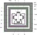
图1为本发明提供的一种实施例所述的采用双保护环的低失调霍尔器件的俯视示意图;FIG. 1 is a schematic top view of a low-offset Hall device using double guard rings according to an embodiment of the present invention;
图2为本发明提供的一种实施例所述的采用双保护环的低失调霍尔器件中N阱有源区与外轮廓的相对位置示意图;2 is a schematic diagram of the relative position of the N-well active region and the outer contour in the low-offset Hall device using double guard rings according to an embodiment of the present invention;
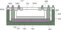
图3为本发明提供的一种实施例所述的采用双保护环的低失调霍尔器件的剖面结构示意图;3 is a schematic cross-sectional structure diagram of a low-offset Hall device using double guard rings according to an embodiment of the present invention;
图4为本发明提供的一种实施例所述的采用双保护环的低失调霍尔器件的双保护环结构示意图;FIG. 4 is a schematic diagram of a double guard ring structure of a low offset Hall device using double guard rings according to an embodiment of the present invention;
图5为本发明提供的一种实施例所述的采用双保护环的低失调霍尔器件的工作偏置结构示意图;FIG. 5 is a schematic diagram of a working bias structure of a low-offset Hall device using double guard rings according to an embodiment of the present invention;
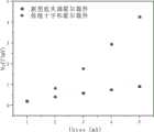
图6为本发明与传统十字形霍尔器件结构进行三维仿真得到的输出失调对比图。FIG. 6 is a comparison diagram of output offset obtained by three-dimensional simulation between the present invention and the traditional cross-shaped Hall device structure.
具体实施方式Detailed ways
为使本发明的上述目的、特征和优点能够更加明显易懂,下面结合说明书附图对本发明的具体实施方式做详细的说明。In order to make the above objects, features and advantages of the present invention more obvious and comprehensible, specific implementations of the present invention will be described in detail below in conjunction with the accompanying drawings.
在下面的描述中阐述了很多具体细节以便于充分理解本发明,但是本发明还可以采用其他不同于在此描述的其它方式来实施,本领域技术人员可以在不违背本发明内涵的情况下做类似推广,因此本发明不受下面公开的具体实施例的限制。In the following description, a lot of specific details are set forth in order to fully understand the present invention, but the present invention can also be implemented in other ways different from those described here, and those skilled in the art can do it without departing from the meaning of the present invention. By analogy, the present invention is therefore not limited to the specific examples disclosed below.
其次,本发明结合示意图进行详细描述,在详述本发明实施例时,为便于说明,表示器件结构的剖面图会不依一般比例作局部放大,而且所述示意图只是示例,其在此不应限制本发明保护的范围。此外,在实际制作中应包含长度、宽度及深度的三维空间尺寸。Secondly, the present invention is described in detail in combination with schematic diagrams. When describing the embodiments of the present invention in detail, for the convenience of explanation, the cross-sectional view showing the device structure will not be partially enlarged according to the general scale, and the schematic diagram is only an example, and it should not be limited here. The protection scope of the present invention. In addition, the three-dimensional space dimensions of length, width and depth should be included in actual production.
再其次,此处所称的“一个实施例”或“实施例”是指可包含于本发明至少一个实现方式中的特定特征、结构或特性。在本说明书中不同地方出现的“在一个实施例中”并非均指同一个实施例,也不是单独的或选择性的与其他实施例互相排斥的实施例。Second, "one embodiment" or "embodiment" referred to herein refers to a specific feature, structure or characteristic that may be included in at least one implementation of the present invention. "In one embodiment" appearing in different places in this specification does not all refer to the same embodiment, nor is it a separate or selective embodiment that is mutually exclusive with other embodiments.
实施例1Example 1
参照图1和图3为本发明提供的一种实施例所述的采用双保护环的低失调霍尔器件的俯视示意图和剖面结构示意图,本实施例提供了一种采用双保护环的低失调霍尔器件,包括,Referring to FIG. 1 and FIG. 3, it is a schematic top view and a schematic cross-sectional structure diagram of a low offset Hall device using double guard rings according to an embodiment of the present invention. This embodiment provides a low offset Hall device using double guard rings. Hall devices, including,
横向层组100,横向层组100包括P型衬底101、设置于P型衬底101中心区域的N+埋层102和设置于N+埋层102顶部中心区域的P-埋层103,P-埋层103上方设置有N阱有源区104,N+埋层102和P-埋层103形成横向保护环;The
N+埋层102处于P型衬底101中心上方,N+埋层102部分嵌于P型衬底101中。The N+ buried
具体的,P型衬底101可以为半导体硅材料,Specifically, the P-
侧围层组200,侧围层组200包括设置于N阱有源区104外侧的P型外延层201,P型外延层201中设置有与N+埋层102顶部连接的高压N阱202,P型外延层201中设置有与P型衬底101顶部连接的高压P阱203,高压P阱203设置于高压N阱202外侧,P型外延层201和高压N阱202形成纵向保护环。The side surrounding
高压P阱203和高压N阱202之间间隔设置有一定厚度的P型外延层201。A P-
需要说明的是,本发明所提出的双保护环,分别是纵向保护环和横向保护环,参照图4。横向保护环是N+埋层102和P-埋层103之间形成的PN结。纵向保护环是在高压N阱202和P型外延层201之间形成的PN结。It should be noted that the double guard rings proposed in the present invention are respectively a longitudinal guard ring and a transverse guard ring, as shown in FIG. 4 . The lateral guard ring is a PN junction formed between the N+ buried
进一步的,参照图2,侧围层组200为对称结构,关于第一对称轴Y1对称;N阱有源区104为对称结构,关于第二对称轴Y2对称,第一对称轴Y1和第二对称轴Y2重合。Further, referring to FIG. 2 , the lateral surrounding
具体的,参照图2(a),所述正方形侧环组件200关于第一对称轴Y1对称轴对称,所述切角正方形N阱有源区104关于第二对称轴Y2对称,所述第一N+区104a均匀分布在N阱有源区104边缘,关于第二对称轴Y2对称,所述第二N+区104b均匀分布在N阱有源区104边缘,关于第二对称轴Y2对称,第一N+区104a和第二N+区104b平行于N阱有源区104边缘放置。第二N+区104b分布在相邻两个第一N+区中心的N阱有源区104上。Specifically, referring to FIG. 2( a ), the square
参照图2(b),所述正八边形侧环组件200关于第一对称轴Y1对称轴对称,所述切角菱形N阱有源区104关于第二对称轴Y2对称,所述第一N+区104a均匀分布在N阱有源区104边缘,关于第二对称轴Y2对称,所述第二N+区104b均匀分布在N阱有源区104边缘,关于第二对称轴Y2对称,第一N+区104a和第二N+区104b平行于N阱有源区104边缘放置。第二N+区104b分布在相邻两个第一N+区中心的N阱有源区104上。Referring to FIG. 2( b ), the regular octagonal
参照图2(c),所述正方形侧环组件200关于第一对称轴Y1对称轴对称,所述切角菱形N阱有源区104关于第二对称轴Y2对称,所述第一N+区104a均匀分布在N阱有源区104边缘,关于第二对称轴Y2对称,所述第二N+区104b均匀分布在N阱有源区104边缘,关于第二对称轴Y2对称,第一N+区104a和第二N+区104b平行于N阱有源区104边缘放置。第二N+区104b分布在相邻两个第一N+区中心的N阱有源区104上。Referring to FIG. 2(c), the square
参照图2(d),所述圆形侧环组件200关于第一对称轴Y1对称轴对称,所述切角菱形N阱有源区104关于第二对称轴Y2对称,所述第一N+区104a均匀分布在N阱有源区104边缘,关于第二对称轴Y2对称,所述第二N+区104b均匀分布在N阱有源区104边缘,关于第二对称轴Y2对称,第一N+区104a和第二N+区104b平行于N阱有源区104边缘放置。第二N+区104b分布在相邻两个第一N+区中心的N阱有源区104上。Referring to FIG. 2( d ), the circular
N阱有源区104的边缘均匀分布设置有第一N+区104a,第一N+区104a关于第二对称轴Y2对称,第一N+区104a平行于N阱有源区104的边缘放置。The edge of the N-well
四个第一N+区104a上均设置有金属,形成四个偏置电极A、B、C和D。Metal is disposed on the four
相邻的第一N+区104a中心的N阱有源区中设置有第二N+区104b,第二N+区104b关于第二对称轴Y2对称,第二N+区104b平行于N阱有源区104的边缘放置;A
第一N+区104a尺寸大于第二N+区104b。The size of the
对角的两个第一N+区104a距其之间的第二N+区104b的距离相同。Diagonally two
四个第二N+区104b上均设置有金属,形成四个输出电极E、F、G和H;Metal is provided on the four
相对的两个输出电极E和H以及F和G通过金属连线短接。The two opposite output electrodes E and H and F and G are short-circuited through metal wires.
高压N阱202表面设置有第三N+区104c,第三N+区104c上设置有金属,形成第一接触电极J。A
N阱有源区104上方非电极部分覆盖有第一P+区104d。The non-electrode portion above the N-well
高压P阱203表面设有第二P+区203a,第二P+区203a上设置有金属,形成第二接触电极K。A
在第一N+区104a和第三N+区104c之间、第一N+区104a和第一P+区104d、第三N+区104c和第二P+区203a之间设有隔离浅沟槽300。Isolation
进一步地,对所用层次结构的作用进行详细阐述,Further, elaborating on the role of the hierarchy used,
P-埋层103可以控制掺杂分布,和N+埋层102之间形成更加均匀的PN结,即横向PN结,改善N阱有源区104底部杂质浓度分布,从而提高霍尔器件的对称性,减小输出失调。The P-buried
横向PN结形成内建电场可以减小N阱有源区104底部的电流损耗,降低器件工作时外部噪声干扰。The built-in electric field formed by the lateral PN junction can reduce the current loss at the bottom of the N-well
第一P+区104d和N阱104之间形成耗尽层,从而增加电流输运路径,避免短路效应,也可以减小N阱厚度来增加其电流相关灵敏度。第一P+区104d还可以形成PMOS晶体管,由于PMOS管是“埋沟”器件,可以有效降低器件的闪烁噪声和电流的表面损耗,增大霍尔电压。A depletion layer is formed between the
高压N阱202与P型外延层201之间形成PN结,即为纵向保护环有效减小横向漏电流和1/f噪声。A PN junction is formed between the high-voltage N-well 202 and the P-
本发明采用N+埋层102和P-埋层103形成横向PN结作为保护环,代替了原本P型外延层与N阱有源区之间的PN结,有效改善了N阱有源区104的杂质浓度分布,减小了霍尔器件由于N阱有源区104杂质浓度呈高斯分布造成的输出失调,而且所形成的的PN结耗尽层更宽,并进一步提高霍尔器件的抗干扰能力,减小底部漏电流。The present invention uses the N+ buried
本发明采用高压N阱202与N+埋层102接触,将高压N阱202顶部的第一接触电极J接高电平,从而使N+埋层102接高电平,N+埋层102和P-埋层103之间的横向PN结反偏,进一步加宽横向PN结耗尽层,使霍尔器件的抗干扰能力更强,失调更小,同时这种方式减小了N阱有源区104的有效深度,提高霍尔器件的灵敏度。高压N阱202还可以与P型外延层201之间形成纵向PN结,进一步减小霍尔器件的横向漏电流和噪声,对霍尔器件起到了双重保护。The present invention adopts the high-voltage N well 202 to contact the N+ buried
实施例2Example 2
参照图5和6,本实施例还提出了上述采用双保护环的低失调霍尔器件的使用方法,为:Referring to Figures 5 and 6, this embodiment also proposes the method of using the above-mentioned low-offset Hall device with double guard rings, which is:
所提出的霍尔器件的偏置电极A、B、C、D中,其中两个相对的偏置电极输入大小相等、方向相反的电流或电压偏置信号,另外两个相对的偏置电极接地,例如偏置电极A和C中输入大小相等、方向相反的电流或电压偏置信号则偏置电极B和D接地;所提出的霍尔器件的两个短接的输出电极E(或H)和F(或G)之间输出霍尔电流或霍尔电压信号;所提出的第一接触电极J接高电平;所提出的第二接触电极K接地。Among the bias electrodes A, B, C, and D of the proposed Hall device, two opposite bias electrodes input current or voltage bias signals of equal size and opposite directions, and the other two opposite bias electrodes are grounded , For example, the bias electrodes A and C are input with equal and opposite current or voltage bias signals, and the bias electrodes B and D are grounded; the two short-circuited output electrodes E (or H) of the proposed Hall device Output Hall current or Hall voltage signal between F and F (or G); the proposed first contact electrode J is connected to high level; the proposed second contact electrode K is grounded.
进一步,所提出的霍尔器件的衬底材料不仅限于硅(Si)半导体,还可以利用锗硅(SiGe)、砷化镓(GaAs)、磷化铟(InP)、氮化镓(GaN)、碳化硅(SiC)和铟镓砷(InGaAs)等多种半导体材料作为衬底。Further, the substrate material of the proposed Hall device is not limited to silicon (Si) semiconductor, but silicon germanium (SiGe), gallium arsenide (GaAs), indium phosphide (InP), gallium nitride (GaN), Various semiconductor materials such as silicon carbide (SiC) and indium gallium arsenide (InGaAs) are used as substrates.
进一步,所提出的霍尔器件的N阱有源区104还可以设计为八边形、菱形和圆形结构。Further, the N-well
制作本发明提出的低失调霍尔器件结构的工艺步骤为:The process steps for making the low offset Hall device structure proposed by the present invention are:
步骤S1,首先在P型衬底101上的中心区域形成N+埋层102。In step S1 , an N+ buried
步骤S2,在P型衬底101上生长一层P型外延层201,并在P型外延层201顶部形成隔离浅沟槽300。In step S2 , a P-
步骤S3,在N+埋层102上方的外延层中形成P-埋层103,P-埋层103底部与N+埋层102顶部连接。In step S3 , a P-buried
步骤S4,在P-埋层103上的P型外延层201中注入N阱有源区104。Step S4 , implanting the N-well
步骤S5,在N阱有源区104周围的P型外延层201中形成高压N阱202,高压N阱底部与N+埋层102顶部相连接。In step S5 , a high voltage N well 202 is formed in the P-
步骤S6,在高压N阱202周围的P型外延层201中形成高压P阱203,高压P阱203底部与P型衬底101相连接。Step S6 , forming a high voltage P well 203 in the P
步骤S7,在N阱有源区104顶部形成第一N+区104a和第二N+区104b,在高压N阱202表面形成第三N+区104c。In step S7 , a
步骤S8,在N阱有源区104表面形成第一P+区104d,在高压P阱203表面形成第二P+区203a。In step S8 , a
步骤S9,在P型外延层201上设有接触孔,形成金属互连线。In step S9, a contact hole is provided on the P-
结合图5中低失调霍尔器件的工作偏置示意图,进一步说明所提出的霍尔器件工作方法:Combined with the working bias diagram of the low offset Hall device in Figure 5, the proposed working method of the Hall device is further explained:
当霍尔偏置电极A、C输入大小相等极性相反的电流偏置,另外两个偏置电极B、D连接到地,无外加磁场时,假设N阱有源区104整体浓度分布均匀,这时四个输出电极E、F、G、H附近的电流密度相同,理想上输出的电压为0。When the Hall bias electrodes A and C input current biases of equal magnitude and opposite polarity, the other two bias electrodes B and D are connected to ground, and there is no external magnetic field, assuming that the overall concentration distribution of the N-well
进一步地,当施加垂直纸面向内的磁场,载流子受到洛伦兹力发生偏转,同时极化四个输出电极,由于实际情况下,霍尔器件有源区杂质分布不均,所以四个输出电极附近的电流密度存在不对称的现象。Furthermore, when a magnetic field perpendicular to the surface of the paper is applied inward, the carriers are deflected by the Lorentz force, and the four output electrodes are polarized at the same time. Due to the uneven distribution of impurities in the active region of the Hall device, the four There is an asymmetry in the current density near the output electrode.
进一步地,本发明中霍尔器件的对角输出电极E和H、F和G短接,迫使电流在有源区中均匀分布,减小了由于电阻率、杂质浓度不均或工艺应力不均产生的失调,实现了静态消除失调信号,且不需要旋转电流技术,减小了前端电路的寄生电容。Further, in the present invention, the diagonal output electrodes E and H, F and G of the Hall device are short-circuited, forcing the current to be evenly distributed in the active region, reducing the resistance due to resistivity, uneven impurity concentration, or uneven process stress. The generated offset realizes the static elimination of the offset signal, and does not require the spinning current technology, which reduces the parasitic capacitance of the front-end circuit.
进一步地,由于第一接触电极J始终接高电平,第二接触电极K始终接地,可以使所述的横向保护环和纵向保护环反偏,减小了漏电流和工作时电路中高频信号干扰,增强了霍尔器件的抗干扰能力。Further, since the first contact electrode J is always connected to a high level and the second contact electrode K is always connected to the ground, the horizontal guard ring and the longitudinal guard ring can be reverse-biased, reducing the leakage current and the high-frequency signal in the circuit during operation. Interference, enhance the anti-interference ability of the Hall device.
参照图6为本发明与传统十字形霍尔器件结构的输出失调对比仿真图。Referring to FIG. 6 , it is a comparison simulation diagram of the output offset between the present invention and the traditional cross-shaped Hall device structure.
具体的,针对图1和图2所示的器件结构,根据高压BCD工艺的工艺流程参数,使用Silvaco TCAD仿真工具对低失调霍尔器件结构进行了器件电学特性仿真,得到图5低失调霍尔器件与传统四接触孔的霍尔器件的输出失调大小的对比,可以发现在0-5mA的偏置电流下,低失调霍尔器件的输出失调始终在1mV以下,而传统十字形霍尔器件输出失调在5mA偏置电流下就达到了4.5mV左右,说明本发明设计的低失调霍尔器件方案具有可行性。Specifically, for the device structure shown in Figure 1 and Figure 2, according to the process parameters of the high-voltage BCD process, the Silvaco TCAD simulation tool was used to simulate the device electrical characteristics of the low-offset Hall device structure, and the low-offset Hall device structure in Figure 5 was obtained. Comparing the output offset of the device with the traditional four-contact Hall device, it can be found that under the bias current of 0-5mA, the output offset of the low-offset Hall device is always below 1mV, while the output of the traditional cross-shaped Hall device The offset reaches about 4.5mV under the bias current of 5mA, which shows that the low offset Hall device solution designed by the present invention is feasible.
重要的是,应注意,在多个不同示例性实施方案中示出的本申请的构造和布置仅是例示性的。尽管在此公开内容中仅详细描述了几个实施方案,但参阅此公开内容的人员应容易理解,在实质上不偏离该申请中所描述的主题的新颖教导和优点的前提下,许多改型是可能的(例如,各种元件的尺寸、尺度、结构、形状和比例、以及参数值(例如,温度、压力等)、安装布置、材料的使用、颜色、定向的变化等)。例如,示出为整体成形的元件可以由多个部分或元件构成,元件的位置可被倒置或以其它方式改变,并且分立元件的性质或数目或位置可被更改或改变。因此,所有这样的改型旨在被包含在本发明的范围内。可以根据替代的实施方案改变或重新排序任何过程或方法步骤的次序或顺序。在权利要求中,任何“装置加功能”的条款都旨在覆盖在本文中所描述的执行所述功能的结构,且不仅是结构等同而且还是等同结构。在不背离本发明的范围的前提下,可以在示例性实施方案的设计、运行状况和布置中做出其他替换、改型、改变和省略。因此,本发明不限制于特定的实施方案,而是扩展至仍落在所附的权利要求书的范围内的多种改型。It is important to note that the construction and arrangement of the application, shown in the various exemplary embodiments, are illustrative only. Although only a few embodiments have been described in detail in this disclosure, it should be readily apparent to those who review this disclosure that many modifications are possible without materially departing from the novel teachings and advantages of the subject matter described in this application. are possible (e.g., variations in dimensions, dimensions, structures, shapes and proportions of various elements, as well as parameter values (e.g., temperature, pressure, etc.), mounting arrangements, use of materials, colors, orientations, etc.). For example, elements shown as integrally formed may be constructed of multiple parts or elements, the position of elements may be inverted or otherwise varied, and the nature or number or positions of discrete elements may be altered or varied. Accordingly, all such modifications are intended to be included within the scope of this invention. The order or sequence of any process or method steps may be varied or re-sequenced according to alternative embodiments. In the claims, any "means-plus-function" clause is intended to cover the structures described herein as performing the recited function and not only structural equivalents but also equivalent structures. Other substitutions, modifications, changes and omissions may be made in the design, operation and arrangement of the exemplary embodiments without departing from the scope of the invention. Accordingly, the invention is not limited to a particular embodiment, but extends to various modifications still falling within the scope of the appended claims.
此外,为了提供示例性实施方案的简练描述,可以不描述实际实施方案的所有特征(即,与当前考虑的执行本发明的最佳模式不相关的那些特征,或于实现本发明不相关的那些特征)。Furthermore, in order to provide a concise description of exemplary embodiments, not all features of an actual embodiment (i.e., those features not relevant to the best mode presently considered for carrying out the invention, or to practicing the invention feature).
应理解的是,在任何实际实施方式的开发过程中,如在任何工程或设计项目中,可做出大量的具体实施方式决定。这样的开发努力可能是复杂的且耗时的,但对于那些得益于此公开内容的普通技术人员来说,不需要过多实验,所述开发努力将是一个设计、制造和生产的常规工作。It should be appreciated that during the development of any actual implementation, as in any engineering or design project, numerous implementation-specific decisions may be made. Such a development effort would be complex and time-consuming, but would be a routine matter of design, fabrication, and production without undue experimentation to those of ordinary skill having the benefit of this disclosure .
应说明的是,以上实施例仅用以说明本发明的技术方案而非限制,尽管参照较佳实施例对本发明进行了详细说明,本领域的普通技术人员应当理解,可以对本发明的技术方案进行修改或者等同替换,而不脱离本发明技术方案的精神和范围,其均应涵盖在本发明的权利要求范围当中。It should be noted that the above embodiments are only used to illustrate the technical solutions of the present invention without limitation, although the present invention has been described in detail with reference to the preferred embodiments, those of ordinary skill in the art should understand that the technical solutions of the present invention can be carried out Modifications or equivalent replacements without departing from the spirit and scope of the technical solution of the present invention shall be covered by the claims of the present invention.
Claims (10)
Translated fromChinesePriority Applications (1)
| Application Number | Priority Date | Filing Date | Title |
|---|---|---|---|
| CN202310388847.0ACN116113309B (en) | 2023-04-13 | 2023-04-13 | A low-offset Hall device using double guard rings and its application method |
Applications Claiming Priority (1)
| Application Number | Priority Date | Filing Date | Title |
|---|---|---|---|
| CN202310388847.0ACN116113309B (en) | 2023-04-13 | 2023-04-13 | A low-offset Hall device using double guard rings and its application method |
Publications (2)
| Publication Number | Publication Date |
|---|---|
| CN116113309Atrue CN116113309A (en) | 2023-05-12 |
| CN116113309B CN116113309B (en) | 2023-07-25 |
Family
ID=86260140
Family Applications (1)
| Application Number | Title | Priority Date | Filing Date |
|---|---|---|---|
| CN202310388847.0AActiveCN116113309B (en) | 2023-04-13 | 2023-04-13 | A low-offset Hall device using double guard rings and its application method |
Country Status (1)
| Country | Link |
|---|---|
| CN (1) | CN116113309B (en) |
Cited By (2)
| Publication number | Priority date | Publication date | Assignee | Title |
|---|---|---|---|---|
| CN117279481A (en)* | 2023-11-23 | 2023-12-22 | 深圳市晶扬电子有限公司 | High-performance vertical Hall device |
| CN118591264A (en)* | 2024-07-31 | 2024-09-03 | 南京邮电大学 | High-sensitivity four-hole vertical Hall device and its use, preparation and coupling method |
Citations (10)
| Publication number | Priority date | Publication date | Assignee | Title |
|---|---|---|---|---|
| US20050179093A1 (en)* | 2004-02-17 | 2005-08-18 | Silicon Space Technology Corporation | Buried guard ring and radiation hardened isolation structures and fabrication methods |
| CN102236736A (en)* | 2011-07-08 | 2011-11-09 | 南京邮电大学 | Circuit simulation model of crossed CMOS (complementary metal-oxide-semiconductor) integrated Hall magnetic sensor |
| JP2012212700A (en)* | 2011-03-30 | 2012-11-01 | Asahi Kasei Electronics Co Ltd | Hall element and semiconductor device with hall element |
| US20130307609A1 (en)* | 2012-05-15 | 2013-11-21 | Infineon Technologies Ag | Hall Effect Device |
| US20160079344A1 (en)* | 2014-09-11 | 2016-03-17 | Semiconductor Components Industries, Llc | Electronic Device Including An Isolation Structure |
| US20160268498A1 (en)* | 2015-03-13 | 2016-09-15 | Infineon Technologies Ag | Method for doping an active hall effect region of a hall effect device and hall effect device having a doped active hall effect region |
| CN106449969A (en)* | 2016-12-01 | 2017-02-22 | 上海南麟电子股份有限公司 | Hall sensor and preparation method thereof |
| US20180315919A1 (en)* | 2017-04-28 | 2018-11-01 | Ablic Inc. | Semiconductor device |
| US20190086484A1 (en)* | 2017-09-20 | 2019-03-21 | Texas Instruments Incorporated | Vertical hall-effect sensor for detecting two-dimensional in-plane magnetic fields |
| CN110501031A (en)* | 2018-05-16 | 2019-11-26 | 英飞凌科技股份有限公司 | Compensation for mechanical stress of Hall sensor circuits integrated in semiconductor substrates |
- 2023
- 2023-04-13CNCN202310388847.0Apatent/CN116113309B/enactiveActive
Patent Citations (10)
| Publication number | Priority date | Publication date | Assignee | Title |
|---|---|---|---|---|
| US20050179093A1 (en)* | 2004-02-17 | 2005-08-18 | Silicon Space Technology Corporation | Buried guard ring and radiation hardened isolation structures and fabrication methods |
| JP2012212700A (en)* | 2011-03-30 | 2012-11-01 | Asahi Kasei Electronics Co Ltd | Hall element and semiconductor device with hall element |
| CN102236736A (en)* | 2011-07-08 | 2011-11-09 | 南京邮电大学 | Circuit simulation model of crossed CMOS (complementary metal-oxide-semiconductor) integrated Hall magnetic sensor |
| US20130307609A1 (en)* | 2012-05-15 | 2013-11-21 | Infineon Technologies Ag | Hall Effect Device |
| US20160079344A1 (en)* | 2014-09-11 | 2016-03-17 | Semiconductor Components Industries, Llc | Electronic Device Including An Isolation Structure |
| US20160268498A1 (en)* | 2015-03-13 | 2016-09-15 | Infineon Technologies Ag | Method for doping an active hall effect region of a hall effect device and hall effect device having a doped active hall effect region |
| CN106449969A (en)* | 2016-12-01 | 2017-02-22 | 上海南麟电子股份有限公司 | Hall sensor and preparation method thereof |
| US20180315919A1 (en)* | 2017-04-28 | 2018-11-01 | Ablic Inc. | Semiconductor device |
| US20190086484A1 (en)* | 2017-09-20 | 2019-03-21 | Texas Instruments Incorporated | Vertical hall-effect sensor for detecting two-dimensional in-plane magnetic fields |
| CN110501031A (en)* | 2018-05-16 | 2019-11-26 | 英飞凌科技股份有限公司 | Compensation for mechanical stress of Hall sensor circuits integrated in semiconductor substrates |
Cited By (4)
| Publication number | Priority date | Publication date | Assignee | Title |
|---|---|---|---|---|
| CN117279481A (en)* | 2023-11-23 | 2023-12-22 | 深圳市晶扬电子有限公司 | High-performance vertical Hall device |
| CN117279481B (en)* | 2023-11-23 | 2024-02-09 | 深圳市晶扬电子有限公司 | High-performance vertical Hall device |
| CN118591264A (en)* | 2024-07-31 | 2024-09-03 | 南京邮电大学 | High-sensitivity four-hole vertical Hall device and its use, preparation and coupling method |
| CN118591264B (en)* | 2024-07-31 | 2024-10-11 | 南京邮电大学 | High-sensitivity four-hole vertical Hall device and using, preparing and coupling methods thereof |
Also Published As
| Publication number | Publication date |
|---|---|
| CN116113309B (en) | 2023-07-25 |
Similar Documents
| Publication | Publication Date | Title |
|---|---|---|
| CN116113309B (en) | A low-offset Hall device using double guard rings and its application method | |
| KR101446387B1 (en) | Io esd device and methods for forming the same | |
| US9343459B2 (en) | Method for creating the high voltage complementary BJT with lateral collector on bulk substrate with resurf effect | |
| US11024649B2 (en) | Integrated circuit with resurf region biasing under buried insulator layers | |
| CN102738245A (en) | Diodes with embedded dummy gate electrodes | |
| US9484525B2 (en) | Hall effect device | |
| CN113690337B (en) | Single photon avalanche diode, manufacturing method thereof and single photon avalanche diode array | |
| US7511346B2 (en) | Design of high-frequency substrate noise isolation in BiCMOS technology | |
| US20230178677A1 (en) | Single-photon avalanche photodiode | |
| CN104134695A (en) | Tunneling field effect transistor and manufacturing method thereof | |
| WO2025102568A1 (en) | Horizontal hall device and preparation method therefor | |
| CN103779429B (en) | High-voltage diode | |
| CN117082961A (en) | Vertical Hall device and preparation method thereof | |
| US9543378B2 (en) | Semiconductor devices and fabrication methods thereof | |
| US7755168B2 (en) | Semiconductor device provided with floating electrode | |
| CN104659023A (en) | Semiconductor structure and forming method thereof | |
| CN205177856U (en) | Zener diode and circuit | |
| CN118591264B (en) | High-sensitivity four-hole vertical Hall device and using, preparing and coupling methods thereof | |
| CN109817726B (en) | Asymmetric transient voltage suppressor apparatus and method of forming | |
| US7598575B1 (en) | Semiconductor die with reduced RF attenuation | |
| CN110349939A (en) | Induction structure and preparation method thereof | |
| US20250306138A1 (en) | Vertical hall element | |
| CN118434265B (en) | Single-chip integrated 3D Hall device and preparation method thereof | |
| CN105355594B (en) | Integrated circuit structure | |
| US20250311640A1 (en) | Vertical hall element |
Legal Events
| Date | Code | Title | Description |
|---|---|---|---|
| PB01 | Publication | ||
| PB01 | Publication | ||
| SE01 | Entry into force of request for substantive examination | ||
| SE01 | Entry into force of request for substantive examination | ||
| GR01 | Patent grant | ||
| GR01 | Patent grant |