CN116111990A - Comparators used in full bridge rectifiers, full bridge rectifiers and electronics - Google Patents
Comparators used in full bridge rectifiers, full bridge rectifiers and electronicsDownload PDFInfo
- Publication number
- CN116111990A CN116111990ACN202211326699.1ACN202211326699ACN116111990ACN 116111990 ACN116111990 ACN 116111990ACN 202211326699 ACN202211326699 ACN 202211326699ACN 116111990 ACN116111990 ACN 116111990A
- Authority
- CN
- China
- Prior art keywords
- pmos transistor
- transistor
- source
- drain
- nmos
- Prior art date
- Legal status (The legal status is an assumption and is not a legal conclusion. Google has not performed a legal analysis and makes no representation as to the accuracy of the status listed.)
- Granted
Links
Images


Classifications
- H—ELECTRICITY
- H03—ELECTRONIC CIRCUITRY
- H03K—PULSE TECHNIQUE
- H03K5/00—Manipulating of pulses not covered by one of the other main groups of this subclass
- H03K5/22—Circuits having more than one input and one output for comparing pulses or pulse trains with each other according to input signal characteristics, e.g. slope, integral
- H03K5/24—Circuits having more than one input and one output for comparing pulses or pulse trains with each other according to input signal characteristics, e.g. slope, integral the characteristic being amplitude
- H03K5/2472—Circuits having more than one input and one output for comparing pulses or pulse trains with each other according to input signal characteristics, e.g. slope, integral the characteristic being amplitude using field effect transistors
- H—ELECTRICITY
- H02—GENERATION; CONVERSION OR DISTRIBUTION OF ELECTRIC POWER
- H02M—APPARATUS FOR CONVERSION BETWEEN AC AND AC, BETWEEN AC AND DC, OR BETWEEN DC AND DC, AND FOR USE WITH MAINS OR SIMILAR POWER SUPPLY SYSTEMS; CONVERSION OF DC OR AC INPUT POWER INTO SURGE OUTPUT POWER; CONTROL OR REGULATION THEREOF
- H02M7/00—Conversion of AC power input into DC power output; Conversion of DC power input into AC power output
- H02M7/02—Conversion of AC power input into DC power output without possibility of reversal
- H02M7/04—Conversion of AC power input into DC power output without possibility of reversal by static converters
- H02M7/12—Conversion of AC power input into DC power output without possibility of reversal by static converters using discharge tubes with control electrode or semiconductor devices with control electrode
- H02M7/21—Conversion of AC power input into DC power output without possibility of reversal by static converters using discharge tubes with control electrode or semiconductor devices with control electrode using devices of a triode or transistor type requiring continuous application of a control signal
- H02M7/217—Conversion of AC power input into DC power output without possibility of reversal by static converters using discharge tubes with control electrode or semiconductor devices with control electrode using devices of a triode or transistor type requiring continuous application of a control signal using semiconductor devices only
- H02M7/219—Conversion of AC power input into DC power output without possibility of reversal by static converters using discharge tubes with control electrode or semiconductor devices with control electrode using devices of a triode or transistor type requiring continuous application of a control signal using semiconductor devices only in a bridge configuration
- Y—GENERAL TAGGING OF NEW TECHNOLOGICAL DEVELOPMENTS; GENERAL TAGGING OF CROSS-SECTIONAL TECHNOLOGIES SPANNING OVER SEVERAL SECTIONS OF THE IPC; TECHNICAL SUBJECTS COVERED BY FORMER USPC CROSS-REFERENCE ART COLLECTIONS [XRACs] AND DIGESTS
- Y02—TECHNOLOGIES OR APPLICATIONS FOR MITIGATION OR ADAPTATION AGAINST CLIMATE CHANGE
- Y02B—CLIMATE CHANGE MITIGATION TECHNOLOGIES RELATED TO BUILDINGS, e.g. HOUSING, HOUSE APPLIANCES OR RELATED END-USER APPLICATIONS
- Y02B70/00—Technologies for an efficient end-user side electric power management and consumption
- Y02B70/10—Technologies improving the efficiency by using switched-mode power supplies [SMPS], i.e. efficient power electronics conversion e.g. power factor correction or reduction of losses in power supplies or efficient standby modes
Landscapes
- Engineering & Computer Science (AREA)
- Power Engineering (AREA)
- Physics & Mathematics (AREA)
- Nonlinear Science (AREA)
- Rectifiers (AREA)
- Measurement Of Current Or Voltage (AREA)
Abstract
Description
Translated fromChinese技术领域technical field
本公开涉及集成电路技术领域,具体涉及一种用于全桥整流器中的比较器、全桥整流器及电子设备。The disclosure relates to the technical field of integrated circuits, in particular to a comparator used in a full-bridge rectifier, a full-bridge rectifier and electronic equipment.
背景技术Background technique
现有的全桥整流器结构通常采用比较器检测MOS管源、漏两端电压的大小从而导通或者关断MOS管,以实现整流功能。由于使用了比较器,现有的比较器存在失调电压,且该失调电压随温度和工艺的变化而变化,使得整流器的导通与关断受限于比较器的响应速度。慢的比较器速度会导致整流器不能及时关断,额外的反向泄漏电流甚至会严重地降低整流器的效率。The existing full-bridge rectifier structure usually uses a comparator to detect the voltage across the source and drain of the MOS tube to turn on or off the MOS tube to realize the rectification function. Due to the use of the comparator, the existing comparator has an offset voltage, and the offset voltage changes with changes in temperature and process, so that the turn-on and turn-off of the rectifier is limited by the response speed of the comparator. A slow comparator speed will cause the rectifier not to turn off in time, and the extra reverse leakage current will even seriously reduce the efficiency of the rectifier.
发明内容Contents of the invention
为了解决相关技术中的问题,本公开实施例提供一种用于全桥整流器中的比较器、全桥整流器及电子设备。In order to solve the problems in the related art, embodiments of the present disclosure provide a comparator used in a full-bridge rectifier, a full-bridge rectifier and electronic equipment.
第一方面,本公开实施例中提供了一种用于全桥整流器中的比较器。In a first aspect, embodiments of the present disclosure provide a comparator used in a full-bridge rectifier.
具体地,所述比较器的输出端为所述全桥整流器中的NMOS管提供控制信号,所述比较器包括:偏置电流电路和共栅极比较电路;所述偏置电流电路用于向所述共栅极比较电路提供电流偏置;所述共栅极比较电路包括NMOS管MN1,所述NMOS管MN1与所述NMOS管的类型相同且尺寸不同;其中,所述NMOS管MN1的源极作为所述共栅极比较电路的一个输入端接地电平pvss,所述共栅极比较电路的另一个输入端接所述全桥整流器的输入电压Vinp。Specifically, the output terminal of the comparator provides a control signal for the NMOS transistor in the full-bridge rectifier, and the comparator includes: a bias current circuit and a common gate comparison circuit; the bias current circuit is used to provide The common gate comparison circuit provides current bias; the common gate comparison circuit includes an NMOS transistor MN1 , and the NMOS transistor MN1 is the same type as the NMOS transistor and has a different size; wherein, the NMOS transistor M The source ofN1 is used as one input terminal of the common gate comparison circuit to ground level pvss, and the other input terminal of the common gate comparison circuit is connected to the input voltage Vinp of the full bridge rectifier.
根据本公开的实施例,所述偏置电流电路包括电阻R1、PMOS管Mp1、PMOS管Mp4和恒流源Iref;所述共栅极比较电路包括PMOS管Mp2、PMOS管Mp3、PMOS管Mp5、PMOS管Mp6、NMOS管MN2、NMOS管MN3 、NMOS管MN4、恒流源I1、和反相器INV1;According to an embodiment of the present disclosure, the bias current circuit includes a resistor R1, a PMOS transistor Mp1 , a PMOS transistor Mp4 and a constant current source Iref ; the common gate comparison circuit includes a PMOS transistor Mp2 and a PMOS transistor Mp3 , PMOS transistor Mp5 , PMOS transistor Mp6 , NMOS transistor MN2 , NMOS transistor MN3 , NMOS transistor MN4 , constant current source I1 , and inverter INV1;
其中,PMOS管Mp1的源极、PMOS管Mp2的源极、PMOS管Mp3的源极、恒流源I1的一端连接电源电压VDD;电阻R1的一端、PMOS管Mp1的栅极、PMOS管Mp2的栅极、PMOS管Mp3的栅极、PMOS管Mp4的漏极共接,电阻R1的另一端连接PMOS管Mp4的栅极、PMOS管Mp5的栅极、PMOS管Mp6的栅极、恒流源Iref的一端;恒流源Iref的另一端、NMOS管MN4的源级接地;NMOS管MN4的漏级连接恒流源I1的另一端、反相器INV1的输入端;反相器INV1的输出端作为所述比较器的第一输出端;Among them, the source of the PMOS transistorMp1 , the source of the PMOS transistorMp2 , the source of the PMOS transistorMp3 , and one end of the constant current sourceI1 are connected to the power supply voltage VDD; one end of the resistor R1, the gate of the PMOS transistorMp1 , the grid of the PMOS transistorMp2 , the grid of the PMOS transistorMp3 , and the drain of the PMOS transistorMp4 are connected together, and the other end of the resistor R1 is connected to the grid of the PMOS transistorMp4 , the grid of the PMOS transistorMp5 , the PMOS The gate of the tube Mp6 , one end of the constant current source Iref ; the other end of the constant current source Iref , the source level of the NMOS tube MN4 is grounded; the drain of the NMOS tube MN4 is connected to the other end of the constant current source I1 , The input terminal of the inverter INV1; the output terminal of the inverter INV1 is used as the first output terminal of the comparator;
PMOS管Mp1的漏极连接PMOS管Mp4的源极;PMOS管Mp2的漏极连接PMOS管Mp5的源极;PMOS管Mp3的漏极连接PMOS管Mp6的源极;PMOS管Mp5的漏极、NMOS管MN2的漏极、NMOS管MN2的栅极、NMOS管MN3的栅极共接;PMOS管Mp6的漏极、NMOS管MN3的漏极、NMOS管MN4的栅极共接;NMOS管MN2的源极接地电平pvss;NMOS管MN3的源极连接NMOS管MN1的漏级,NMOS管MN1的栅级接驱动电源pvdd。The drain of the PMOS transistorMp1 is connected to the source of the PMOS transistorMp4 ; the drain of the PMOS transistorMp2 is connected to the source of the PMOS transistorMp5 ; the drain of the PMOS transistorMp3 is connected to the source of the PMOS transistorMp6 ; The drain ofMp5 , the drain of NMOS transistorMN2 , the gate of NMOS transistorMN2 , and the gate of NMOS transistorMN3 are connected together; the drain of PMOS transistorMp6 , the drain of NMOS transistorMN3 , and the NMOS transistor The gates ofMN4 are connected in common; the source of NMOS transistorMN2 is connected to ground level pvss; the source of NMOS transistorMN3 is connected to the drain of NMOS transistorMN1 , and the gate of NMOS transistorMN1 is connected to driving power pvdd.
根据本公开的实施例,还包括:下降沿校正电路;所述下降沿校正电路包括电阻R2、电阻R3、PMOS管Mp7、PMOS管Mp8、NMOS管MN5、恒流源I2和反相器INV2;According to the embodiment of the present disclosure, it also includes: a falling edge correction circuit; the falling edge correction circuit includes a resistor R2, a resistor R3, a PMOS transistor Mp7 , a PMOS transistor Mp8 , an NMOS transistor MN5 , a constant current source I2 and an inverter. phase device INV2;
其中,PMOS管Mp7的源极、PMOS管Mp8的源极连接电源电压VDD;PMOS管Mp7的漏极连接电阻R2的一端;电阻R2的另一端、电阻R3的一端、PMOS管Mp7的栅极、PMOS管Mp8的栅极共接;电阻R3的另一端连接NMOS管MN5的漏级;恒流源I2的一端接地;NMOS管MN5的源极接地电平pvss,NMOS管MN5的栅极接钳位电压VBN;PMOS管Mp8的漏极、恒流源I2的另一端、反相器INV2的输入端共接;反相器INV2的输出端作为所述比较器的第二输出端。Among them, the source of the PMOS transistorMp7 and the source of the PMOS transistorMp8 are connected to the power supply voltage VDD; the drain of the PMOS transistorMp7 is connected to one end of the resistor R2; the other end of the resistor R2, one end of the resistor R3, and the PMOS transistorMp7 The gate of the PMOS transistorMp8 is connected in common; the other end of the resistor R3 is connected to the drain of the NMOS transistorMN5 ; one end of the constant current sourceI2 is grounded; the source of the NMOS transistorMN5 is grounded at pvss, NMOS The gate of the tube MN5 is connected to the clamping voltage VBN; the drain of the PMOS tube Mp8 , the other end of the constant current sourceI2 , and the input end of the inverter INV2 are connected together; the output end of the inverter INV2 is used as the comparison the second output terminal of the device.
根据本公开的实施例,还包括预充电电路;所述预充电电路包括PMOS管Mp9、放大器;According to an embodiment of the present disclosure, a pre-charging circuit is also included; the pre-charging circuit includes a PMOS transistor Mp9 and an amplifier;
其中,PMOS管Mp9的源极接电源电压VDD,PMOS管Mp9的漏极、PMOS管Mp2的漏级、PMOS管Mp6的漏极共接;所述放大器的正向输入端接地电平pvss,负向输入端接NMOS管MN1的漏级电压vinp1,放大器的输出端接PMOS管Mp9的栅极。Wherein, the source of the PMOS transistorMp9 is connected to the power supply voltage VDD, the drain of the PMOS transistorMp9 , the drain of the PMOS transistorMp2 , and the drain of the PMOS transistorMp6 are connected together; the positive input terminal of the amplifier is grounded level pvss, the negative input terminal is connected to the drain voltage vinp1 of the NMOS transistor MN1, and the output terminal of the amplifier is connected to the gate of the PMOS transistorMp9 .
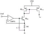
根据本公开的实施例,所述恒流源Iref包括比较器CMP3、PMOS管Mp10、PMOS管Mp11、NMOS管MN6、电阻R4和电容C;According to an embodiment of the present disclosure, the constant current source Iref includes a comparator CMP3 , a PMOS transistor Mp10 , a PMOS transistor Mp11 , an NMOS transistor MN6 , a resistor R4 and a capacitor C;
其中,PMOS管Mp10的源极、PMOS管Mp11的源极接电源电压VDD;PMOS管Mp10的漏极、PMOS管Mp10的栅极、PMOS管Mp11的栅极、NMOS管MN6的漏级共接;NMOS管MN6的源级、电阻R4的一端、比较器CMP3的负向输入端共接;电阻R4的另一端、电容C的下级板接地;电容C的上极板、NMOS管MN6的栅极、比较器CMP3的输出端共接;比较器CMP4的正向输入端接标准电压Vref。Among them, the source of the PMOS transistor Mp10 and the source of the PMOS transistor Mp11 are connected to the power supply voltage VDD; the drain of the PMOS transistor Mp10 , the gate of the PMOS transistor Mp10 , the gate of the PMOS transistor Mp11 , and the NMOS transistor MN6 The drain level of the NMOS tube MN6 is connected together; the source level of the NMOS tube M N6, one end of the resistor R4, and the negative input end of the comparator CMP3 are connected together; the other end of the resistor R4 and the lower plate of the capacitor C are grounded; the upper plate of the capacitor C, The gate of the NMOS transistorMN6 is connected to the output terminal of the comparator CMP3; the positive input terminal of the comparator CMP4 is connected to the standard voltage Vref.
第二方面,本公开实施例中提供了一种如第一方面任一项所述的全桥整流器。In a second aspect, embodiments of the present disclosure provide a full-bridge rectifier according to any one of the first aspect.
根据本公开的实施例,所述全桥整流器包括:一对交又耦合的PMOS管P1和PMOS管P2、NMOS管N1、NMOS管N2以及如权利要求1-5任一项所述的比较器CMP1、比较器CMP2;其中,比较器CMP1输出端为所述全桥整流器中的NMOS管N1提供控制信号;比较器CMP2输出端为所述全桥整流器中的NMOS管N2提供控制信号;According to an embodiment of the present disclosure, the full-bridge rectifier includes: a pair of alternating and coupled PMOS transistors P1 and PMOS transistors P2, NMOS transistor N1, NMOS transistor N2, and the comparator according to any one of claims 1-5 CMP1, comparator CMP2; wherein, the comparator CMP1 output terminal provides a control signal for the NMOS transistor N1 in the full-bridge rectifier; the comparator CMP2 output terminal provides a control signal for the NMOS transistor N2 in the full-bridge rectifier;
其中,PMOS管P1的漏级、PMOS管P2的栅级、全桥整流器的一个输入端、NMOS管N1的漏极共接;PMOS管P2的漏级、PMOS管P1的栅级、全桥整流器的另一个输入端、NMOS管N2的漏极共接;PMOS管P1的源级、PMOS管P2的源级接电源电压;NMOS管N1的源极、NMOS管N2的源级均接地。Among them, the drain of PMOS transistor P1, the gate of PMOS transistor P2, an input terminal of the full-bridge rectifier, and the drain of NMOS transistor N1 are connected in common; the drain of PMOS transistor P2, the gate of PMOS transistor P1, and the full-bridge rectifier The other input end of the NMOS transistor N2 is connected to the drain; the source of the PMOS transistor P1 and the source of the PMOS transistor P2 are connected to the power supply voltage; the source of the NMOS transistor N1 and the source of the NMOS transistor N2 are both grounded.
第三方面,本公开实施例中提供了一种如第二方面所述的全桥整流器的工作方法,所述方法包括:所述比较器检测所述全桥整流器输入端的节点电压与地电平的大小关系,当节点电压小于地电平时,输出高电平控制NMOS管导通;当节点电压大于NMOS管的VDS电压时,输出低电平控制NMOS管关断。In a third aspect, an embodiment of the present disclosure provides a working method of the full-bridge rectifier as described in the second aspect, the method includes: the comparator detects the node voltage and the ground level of the input terminal of the full-bridge rectifier When the node voltage is lower than the ground level, the output high level controls the NMOS tube to turn on; when the node voltage is greater than the VDS voltage of the NMOS tube, the output low level controls the NMOS tube to turn off.
第四方面,本公开实施例中提供了一种电子设备,包括如第二方面任一项所述的全桥整流器。In a fourth aspect, an embodiment of the present disclosure provides an electronic device, including the full-bridge rectifier according to any one of the second aspect.
本公开实施例提供的技术方案可以包括以下有益效果:The technical solutions provided by the embodiments of the present disclosure may include the following beneficial effects:
本公开实施例提供的用于全桥整流器中的比较器,所述比较器的输出端为所述全桥整流器中的NMOS管提供控制信号,所述比较器包括:偏置电流电路和共栅极比较电路;所述偏置电流电路用于向所述共栅极比较电路提供电流偏置;所述共栅极比较电路包括NMOS管MN1,所述NMOS管MN1与所述NMOS管的类型相同且尺寸不同;其中,所述NMOS管MN1的源极作为所述共栅极比较电路的一个输入端接地电平pvss,所述共栅极比较电路的另一个输入端接所述全桥整流器的输入电压Vinp。上述技术方案通过设置与被驱动的NMOS管的类型相同且尺寸不同的NMOS管MN1,由于可以配置二者的尺寸比例并且该比例是已知的,从而通过调节偏置电流电路的偏置电流即可确定比较器的反转电压。此时,由于偏置电流可以设置为不受温度漂移、工艺误差等影响的恒定电流,因此确定的翻转点所对应的功率管电流也不随温度漂移和工艺误差等因素影响,具有较好的精度。In the comparator used in the full-bridge rectifier provided by the embodiment of the present disclosure, the output terminal of the comparator provides a control signal for the NMOS transistor in the full-bridge rectifier, and the comparator includes: a bias current circuit and a common gate pole comparison circuit; the bias current circuit is used to provide current bias to the common gate comparison circuit; the common gate comparison circuit includes an NMOS transistor MN1 , and the NMOS transistor MN1 and the NMOS transistor The types are the same and the sizes are different; wherein, the source of the NMOS transistor MN1 is used as the ground level pvss of one input terminal of the common gate comparison circuit, and the other input terminal of the common gate comparison circuit is connected to the full The input voltage Vinp of the bridge rectifier. The above technical solution sets the NMOS transistor MN1 of the same type and different size as the driven NMOS transistor. Since the size ratio of the two can be configured and the ratio is known, the bias current of the bias current circuit can be adjusted The inversion voltage of the comparator can be determined. At this time, since the bias current can be set as a constant current that is not affected by temperature drift, process error, etc., the power tube current corresponding to the determined flip point is not affected by factors such as temperature drift and process error, and has good accuracy. .
应当理解的是,以上的一般描述和后文的细节描述仅是示例性和解释性的,并不能限制本公开。It is to be understood that both the foregoing general description and the following detailed description are exemplary and explanatory only and are not restrictive of the present disclosure.
附图说明Description of drawings
结合附图,通过以下非限制性实施方式的详细描述,本公开的其它特征、目的和优点将变得更加明显。在附图中。Other features, objects and advantages of the present disclosure will become more apparent through the following detailed description of non-limiting embodiments in conjunction with the accompanying drawings. In the attached picture.
图1示出根据本公开实施例的全桥整流器的结构示意图。FIG. 1 shows a schematic structural diagram of a full-bridge rectifier according to an embodiment of the present disclosure.
图2示出根据本公开实施例的用于全桥整流器中的比较器的结构示意图。FIG. 2 shows a schematic structural diagram of a comparator used in a full-bridge rectifier according to an embodiment of the present disclosure.
图3示出根据本公开另一实施例的用于全桥整流器中的比较器的结构示意图。FIG. 3 shows a schematic structural diagram of a comparator used in a full-bridge rectifier according to another embodiment of the present disclosure.
图4示出根据本公开实施例的恒流源Iref的结构示意图。FIG. 4 shows a schematic structural diagram of a constant current source Iref according to an embodiment of the present disclosure.
图5示出根据本公开实施例的电子设备的结构框图。FIG. 5 shows a structural block diagram of an electronic device according to an embodiment of the present disclosure.
具体实施方式Detailed ways
下文中,将参考附图详细描述本公开的示例性实施例,以使本领域技术人员可容易地实现它们。此外,为了清楚起见,在附图中省略了与描述示例性实施例无关的部分。Hereinafter, exemplary embodiments of the present disclosure will be described in detail with reference to the accompanying drawings so that those skilled in the art can easily realize them. Also, for clarity, parts not related to describing the exemplary embodiments are omitted in the drawings.
在本公开中,应理解,诸如“包括”或“具有”等的术语旨在指示本说明书中所公开的特征、数字、步骤、行为、部件、部分或其组合的存在,并且不欲排除一个或多个其他特征、数字、步骤、行为、部件、部分或其组合存在或被添加的可能性。In the present disclosure, it should be understood that terms such as "comprising" or "having" are intended to indicate the presence of features, numbers, steps, acts, components, parts or combinations thereof disclosed in the specification, and are not intended to exclude one or a plurality of other features, numbers, steps, acts, parts, parts or combinations thereof exist or are added.
另外还需要说明的是,在不冲突的情况下,本公开中的实施例及实施例中的特征可以相互组合。下面将参考附图并结合实施例来详细说明本公开。In addition, it should be noted that, in the case of no conflict, the embodiments in the present disclosure and the features in the embodiments can be combined with each other. The present disclosure will be described in detail below with reference to the accompanying drawings and embodiments.
现有的全桥整流器结构通常采用比较器检测MOS管源、漏两端电压的大小从而导通或者关断MOS管,以实现整流功能。由于使用了比较器,现有的比较器存在失调电压,且该失调电压随温度和工艺的变化而变化,使得整流器的导通与关断受限于比较器的响应速度。慢的比较器速度会导致整流器不能及时关断,额外的反向泄漏电流甚至会严重地降低整流器的效率。The existing full-bridge rectifier structure usually uses a comparator to detect the voltage across the source and drain of the MOS tube to turn on or off the MOS tube to realize the rectification function. Due to the use of the comparator, the existing comparator has an offset voltage, and the offset voltage changes with changes in temperature and process, so that the turn-on and turn-off of the rectifier is limited by the response speed of the comparator. A slow comparator speed will cause the rectifier not to turn off in time, and the extra reverse leakage current will even seriously reduce the efficiency of the rectifier.
为至少部分地解决发明人发现的现有技术中的问题而提出本公开。The present disclosure is proposed to at least partially solve problems in the prior art discovered by the inventors.
图1示出根据本公开实施例的全桥整流器的结构示意图。FIG. 1 shows a schematic structural diagram of a full-bridge rectifier according to an embodiment of the present disclosure.
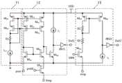
如图1所示,所述全桥整流器包括一对交又耦合的PMOS管P1和PMOS管P2、两个NMOS管(N1和N2)以及两个比较器(CMP1和CMP2)。其中,比较器CMP1输出端为所述全桥整流器中的NMOS管N1提供控制信号;比较器CMP2输出端为所述全桥整流器中的NMOS管N2提供控制信号;PMOS管P1的漏级、PMOS管P2的栅级、全桥整流器的一个输入端(输入电压为Vinp)、NMOS管N1的漏极共接;PMOS管P2的漏级、PMOS管P1的栅级、全桥整流器的另一个输入端(输入电压为Vinn)、NMOS管N2的漏极共接;PMOS管P1的源级、PMOS管P2的源级均接电源电压VDD;NMOS管N1的源极、NMOS管N2的源级均接地。全桥整流器的两个输入端接交流电源;PMOS管P1的源级、PMOS管P2的源级共接作为全桥整流器的输出端。其中,Rc为负载和Cc为电容。As shown in FIG. 1 , the full bridge rectifier includes a pair of alternating and coupled PMOS transistors P1 and PMOS transistors P2 , two NMOS transistors ( N1 and N2 ) and two comparators ( CMP1 and CMP2 ). Wherein, the output terminal of the comparator CMP1 provides a control signal for the NMOS transistor N1 in the full-bridge rectifier; the output terminal of the comparator CMP2 provides a control signal for the NMOS transistor N2 in the full-bridge rectifier; the drain stage of the PMOS transistor P1, the PMOS The gate of the transistor P2, an input terminal of the full-bridge rectifier (the input voltage is Vinp), and the drain of the NMOS transistor N1 are connected in common; the drain of the PMOS transistor P2, the gate of the PMOS transistor P1, and the other input of the full-bridge rectifier terminal (the input voltage is Vinn), and the drain of the NMOS transistor N2 are connected together; the source of the PMOS transistor P1 and the source of the PMOS transistor P2 are both connected to the power supply voltage VDD; the source of the NMOS transistor N1 and the source of the NMOS transistor N2 are connected grounded. The two input terminals of the full-bridge rectifier are connected to the AC power supply; the source stage of the PMOS transistor P1 and the source stage of the PMOS transistor P2 are jointly connected as the output terminals of the full-bridge rectifier. where Rc is the load and Cc is the capacitance.
当节点电压Vinp小于地电平时,输出高电平控制NMOS管N1导通;当节点电压Vinp大于NMOS管N1的VDS电压时,输出低电平控制NMOS管N1关断。同理,比较器CMP2用于检测全桥整流器输入端的节点电压Vinn与地电平的大小关系,当节点电压Vinn小于地电平时,输出高电平控制NMOS管N2导通;当节点电压Vinn大于NMOS管N2的VDS电压时,输出低电平控制NMOS管N2关断。When the node voltage Vinp is lower than the ground level, the output high level controls the NMOS transistor N1 to turn on; when the node voltage Vinp is greater than the VDS voltage of the NMOS transistor N1, the output low level controls the NMOS transistor N1 to turn off. Similarly, the comparator CMP2 is used to detect the relationship between the node voltage Vinn at the input end of the full-bridge rectifier and the ground level. When the node voltage Vinn is lower than the ground level, the output high level controls the NMOS transistor N2 to turn on; when the node voltage Vinn is greater than When the VDS voltage of the NMOS transistor N2 is at a low level, it outputs a low level to control the NMOS transistor N2 to turn off.
图2示出根据本公开实施例的用于全桥整流器中的比较器的结构示意图。FIG. 2 shows a schematic structural diagram of a comparator used in a full-bridge rectifier according to an embodiment of the present disclosure.
如图2所示,所述用于全桥整流器中的比较器即为图1中的比较器CMP1以及比较器CMP2,下面仅以比较器CMP1为例进行示意性说明。As shown in FIG. 2 , the comparators used in the full-bridge rectifier are the comparators CMP1 and CMP2 in FIG. 1 , and the comparator CMP1 is used as an example for schematic illustration below.
比较器CMP1的输出端与所述全桥整流器中的NMOS管N1的栅极连接。比较器CMP1包括偏置电流电路11和共栅极比较电路12。偏置电流电路11用于向共栅极比较电路12提供电流偏置;共栅极比较电路12包括NMOS管MN1,所述NMOS管MN1与NMOS管N1的类型相同且尺寸不同;其中,所述NMOS管MN1的源极作为共栅极比较电路12的一个输入端接地电平pvss,共栅极比较电路12的另一个输入端接所述全桥整流器的输入电压Vinp。The output terminal of the comparator CMP1 is connected to the gate of the NMOS transistor N1 in the full-bridge rectifier. The comparator CMP1 includes a bias
根据本公开实施例的技术方案,通过设置与被驱动的NMOS管的类型相同且尺寸不同的NMOS管MN1,由于可以配置二者的尺寸比例并且该比例是已知的,从而通过调节偏置电流电路的偏置电流即可确定比较器的反转电压。此时,由于偏置电流可以设置为不受温度漂移、工艺误差等影响的恒定电流,因此确定的翻转点所对应的功率管电流也不随温度漂移和工艺误差等因素影响,具有较好的精度。According to the technical solutions of the embodiments of the present disclosure, by setting the NMOS transistor MN1 of the same type and different size as the driven NMOS transistor, since the size ratio of the two can be configured and the ratio is known, by adjusting the bias The bias current of the current circuit determines the inversion voltage of the comparator. At this time, since the bias current can be set as a constant current that is not affected by temperature drift, process error, etc., the power tube current corresponding to the determined flip point is not affected by factors such as temperature drift and process error, and has good accuracy. .
在本公开实施例中,偏置电流电路11包括电阻R1、PMOS管Mp1、PMOS管Mp4和恒流源Iref;共栅极比较电路12包括PMOS管Mp2、PMOS管Mp3、PMOS管Mp5、PMOS管Mp6、NMOS管MN1、NMOS管MN2、NMOS管MN3、NMOS管MN4、恒流源I1、和反相器INV1。In the embodiment of the present disclosure, the bias
其中,PMOS管Mp1的源极、PMOS管Mp2的源极、PMOS管Mp3的源极、恒流源I1的一端连接电源电压VDD;电阻R1的一端、PMOS管Mp1的栅极、PMOS管Mp2的栅极、PMOS管Mp3的栅极、PMOS管Mp4的漏极共接,电阻R1的另一端连接PMOS管Mp4的栅极、PMOS管Mp5的栅极、PMOS管Mp6的栅极、恒流源Iref的一端;恒流源Iref的另一端、NMOS管MN4的源级接地;NMOS管MN4的漏级连接恒流源I1的另一端、反相器INV1的输入端;反相器INV1的输出端作为所述比较器的第一输出端Out1;Among them, the source of the PMOS transistorMp1 , the source of the PMOS transistorMp2 , the source of the PMOS transistorMp3 , and one end of the constant current sourceI1 are connected to the power supply voltage VDD; one end of the resistor R1, the gate of the PMOS transistorMp1 , the grid of the PMOS transistorMp2 , the grid of the PMOS transistorMp3 , and the drain of the PMOS transistorMp4 are connected together, and the other end of the resistor R1 is connected to the grid of the PMOS transistorMp4 , the grid of the PMOS transistorMp5 , the PMOS The gate of the tube Mp6 , one end of the constant current source Iref ; the other end of the constant current source Iref , the source level of the NMOS tube MN4 is grounded; the drain of the NMOS tube MN4 is connected to the other end of the constant current source I1 , The input terminal of the inverter INV1; the output terminal of the inverter INV1 is used as the first output terminal Out1 of the comparator;
PMOS管Mp1的漏极连接PMOS管Mp4的源极;PMOS管Mp2的漏极连接PMOS管Mp5的源极;PMOS管Mp3的漏极连接PMOS管Mp6的源极;PMOS管Mp5的漏极、NMOS管MN2的漏极、NMOS管MN2的栅极、NMOS管MN3的栅极共接;PMOS管Mp6的漏极、NMOS管MN3的漏极、NMOS管MN4的栅极共接;NMOS管MN2的源极接地电平pvss;NMOS管MN3的源极连接NMOS管MN1的漏级,NMOS管MN1的栅级接驱动电源pvdd。本公开方式中,在共栅极比较电路12中增加了NMOS管MN1,以与被驱动的NMOS管的电流匹配,由于二者的压降相同,通过调节偏置电流电路11中恒流源Iref,能够精确控制上升沿的翻转电压,例如Vinp的电压低于零时输出1,从而提前使得电压翻转,以提高比较器的响应速度。The drain of the PMOS transistorMp1 is connected to the source of the PMOS transistorMp4 ; the drain of the PMOS transistorMp2 is connected to the source of the PMOS transistorMp5 ; the drain of the PMOS transistorMp3 is connected to the source of the PMOS transistorMp6 ; The drain ofMp5 , the drain of NMOS transistorMN2 , the gate of NMOS transistorMN2 , and the gate of NMOS transistorMN3 are connected together; the drain of PMOS transistorMp6 , the drain of NMOS transistorMN3 , and the NMOS transistor The gates ofMN4 are connected in common; the source of NMOS transistorMN2 is connected to ground level pvss; the source of NMOS transistorMN3 is connected to the drain of NMOS transistorMN1 , and the gate of NMOS transistorMN1 is connected to driving power pvdd. In the present disclosure, an NMOS transistor MN1 is added in the common
在本公开实施例中,比较器CMP1还包括:下降沿校正电路13;所述下降沿校正电路13包括电阻R2、电阻R3、PMOS管Mp7、PMOS管Mp8、NMOS管MN5、恒流源I2和反相器INV2;其中,PMOS管Mp7的源极、PMOS管Mp8的源极连接电源电压VDD;PMOS管Mp7的漏极连接电阻R2的一端;电阻R2的另一端、电阻R3的一端、PMOS管Mp7的栅极、PMOS管Mp8的栅极共接;电阻R3的另一端连接NMOS管MN5的漏级;恒流源I2的一端接地;NMOS管MN5的源极接地电平pvss,NMOS管MN5的栅极接钳位电压VBN;PMOS管Mp8的漏极、恒流源I2的另一端、反相器INV2的输入端共接;反相器INV2的输出端作为所述比较器的第二输出端Out2。本公开方式中,通过配置电阻R2、电阻R3来调节输出电流,该电流的压摆率不受限,能够快速响应下降沿的翻转。In the embodiment of the present disclosure, the comparator CMP1 further includes: a falling
本公开方式中,反相器INV1的输出端、反相器INV2的输出端连接驱动电路,将上升沿、下降沿的控制信号转换为一个输出信号,之后将驱动电路的输出信号作为全桥整流器中的NMOS管的控制信号。其中,驱动电路的具体结构可以参照现有技术,不作为本申请的重点,在此不予赘述。图3示出根据本公开另一实施例的用于全桥整流器中的比较器的结构示意图。In the disclosed method, the output terminal of the inverter INV1 and the output terminal of the inverter INV2 are connected to the driving circuit, and the control signal of the rising edge and the falling edge is converted into an output signal, and then the output signal of the driving circuit is used as a full-bridge rectifier The control signal of the NMOS tube in it. Wherein, the specific structure of the driving circuit can refer to the prior art, which is not the focus of this application, and will not be described in detail here. FIG. 3 shows a schematic structural diagram of a comparator used in a full-bridge rectifier according to another embodiment of the present disclosure.
如图3所示,所述用于全桥整流器中的比较器还包括:预充电电路14。所述预充电电路14包括PMOS管Mp9、放大器;其中,PMOS管Mp9的源极接电源电压VDD,PMOS管Mp9的漏极、PMOS管Mp2的漏级、PMOS管Mp6的漏极共接;放大器的正向输入端接地电平pvss,负向输入端接NMOS管MN1的漏级电压vinp1(A点),比较器CMP3的输出端接PMOS管Mp9的栅极。As shown in FIG. 3 , the comparator used in the full-bridge rectifier further includes: a
在本公开方式中,考虑到NMOS管MN1的关断受到偏置电流的影响,而偏执电流又不能无限大,为了提高关断速度(提高上升沿翻转的响应速度),可以增加预充电电路,为共栅极比较电路12注入电流,使得图3中B点电压迅速上升,从而进一步提高比较器上升沿的翻转速度。In this disclosure method, considering that the turn-off of the NMOS transistor MN1 is affected by the bias current, and the bias current cannot be infinite, in order to increase the turn-off speed (increase the response speed of the rising edge flip), a pre-charge circuit can be added, The current is injected into the common
图4示出根据本公开实施例的恒流源Iref的结构示意图。FIG. 4 shows a schematic structural diagram of a constant current source Iref according to an embodiment of the present disclosure.
如图4所示,恒流源Iref包括比较器CMP3、PMOS管Mp10、PMOS管Mp11、NMOS管MN6、电阻R4和电容C;其中,PMOS管Mp10的源极、PMOS管Mp11的源极接电源电压VDD;PMOS管Mp10的漏极、PMOS管Mp10的栅极、PMOS管Mp11的栅极、NMOS管MN6的漏级共接;NMOS管MN6的源级、电阻R4的一端、比较器CMP3的负向输入端共接;电阻R4的另一端、电容C的下级板接地;电容C的上极板、NMOS管MN6的栅极、比较器CMP3的输出端共接;比较器CMP3的正向输入端接标准电压Vref。As shown in Figure 4, the constant current source Iref includes a comparator CMP3, a PMOS transistor Mp10 , a PMOS transistor Mp11 , an NMOS transistor MN6 , a resistor R4 and a capacitor C; wherein, the source of the PMOS transistor Mp10 , the PMOS transistor M The source ofp11 is connected to the power supply voltage VDD; the drain of PMOS transistor Mp10 , the gate of PMOS transistor Mp10 , the gate of PMOS transistor Mp11 , and the drain of NMOS transistor MN6 are connected together; the source of NMOS transistor MN6 , one end of the resistor R4, and the negative input end of the comparator CMP3 are connected together; the other end of the resistor R4, and the lower plate of the capacitor C are grounded; the upper plate of the capacitor C, the gate of the NMOS transistor MN6 , and the output of the comparator CMP3 The terminals are connected in common; the positive input terminal of the comparator CMP3 is connected to the standard voltage Vref.
本公开提供的用于全桥整流器中的比较器的工作方法如下:首先设置偏执电流电路输出的偏置电流,之后基于所述偏置电流得到流经所述NMOS管MN1的电流,并基于NMOS管MN1与NMOS管N1的尺寸比得到流经NMOS管N1的电流,最后基于流经NMOS管N1的电流得到比较器的反转电压。当进行NMOS管N1的栅极开启相位检测时,经共栅极比较电路输出比较结果,当进行NMOS管N1的栅极关断相位检测时,经由下降沿校正电路输出比较结果。进一步地,当进行NMOS管N1的栅极开启相位检测时,还可以通过预充电电路为所述共栅极比较电路进行预充电,以提高比较器的响应速度。The working method of the comparator used in the full-bridge rectifier provided by the present disclosure is as follows: first, the bias current output by the bias current circuit is set, and then the current flowing through the NMOS transistor MN1 is obtained based on the bias current, and based on The size ratio of the NMOS transistor MN1 to the NMOS transistor N1 obtains the current flowing through the NMOS transistor N1 , and finally obtains the inversion voltage of the comparator based on the current flowing through the NMOS transistor N1 . When the gate-on phase detection of the NMOS transistor N1 is performed, the comparison result is output through the common gate comparison circuit, and when the gate-off phase detection of the NMOS transistor N1 is performed, the comparison result is output through the falling edge correction circuit. Further, when the gate-on phase detection of the NMOS transistor N1 is performed, the common-gate comparison circuit may also be pre-charged through the pre-charge circuit, so as to improve the response speed of the comparator.
本公开还公开了一种电子设备,图5示出根据本公开的实施例的电子设备的结构框图。在本公开实施例中,所述电子设备包括如图1所示的全桥整流器。The present disclosure also discloses an electronic device, and FIG. 5 shows a structural block diagram of the electronic device according to an embodiment of the present disclosure. In an embodiment of the present disclosure, the electronic device includes a full-bridge rectifier as shown in FIG. 1 .
附图中的流程图和框图,图示了按照本公开各种实施例的系统、方法和计算机程序产品的可能实现的体系架构、功能和操作。在这点上,流程图或框图中的每个方框可以代表一个模块、程序段或代码的一部分,所述模块、程序段或代码的一部分包含一个或多个用于实现规定的逻辑功能的可执行指令。也应当注意,在有些作为替换的实现中,方框中所标注的功能也可以以不同于附图中所标注的顺序发生。例如,两个接连地表示的方框实际上可以基本并行地执行,它们有时也可以按相反的顺序执行,这依所涉及的功能而定。也要注意的是,框图和/或流程图中的每个方框、以及框图和/或流程图中的方框的组合,可以用执行规定的功能或操作的专用的基于硬件的系统来实现,或者可以用专用硬件与计算机指令的组合来实现。The flowchart and block diagrams in the Figures illustrate the architecture, functionality, and operation of possible implementations of systems, methods and computer program products according to various embodiments of the present disclosure. In this regard, each block in a flowchart or block diagram may represent a module, program segment, or part of code that includes one or more Executable instructions. It should also be noted that, in some alternative implementations, the functions noted in the block may occur out of the order noted in the figures. For example, two blocks shown in succession may, in fact, be executed substantially concurrently, or they may sometimes be executed in the reverse order, depending upon the functionality involved. It should also be noted that each block of the block diagrams and/or flowchart illustrations, and combinations of blocks in the block diagrams and/or flowchart illustrations, can be implemented by a dedicated hardware-based system that performs the specified functions or operations , or may be implemented by a combination of dedicated hardware and computer instructions.
描述于本公开实施例中所涉及到的单元或模块可以通过软件的方式实现,也可以通过可编程硬件的方式来实现。所描述的单元或模块也可以设置在处理器中,这些单元或模块的名称在某种情况下并不构成对该单元或模块本身的限定。The units or modules involved in the embodiments described in the present disclosure may be implemented by means of software, or may be implemented by means of programmable hardware. The described units or modules may also be set in the processor, and the names of these units or modules do not constitute limitations on the units or modules themselves in some cases.
作为另一方面,本公开还提供了一种计算机可读存储介质,该计算机可读存储介质可以是上述实施例中电子设备或计算机系统中所包含的计算机可读存储介质;也可以是单独存在,未装配入设备中的计算机可读存储介质。计算机可读存储介质存储有一个或者一个以上程序,所述程序被一个或者一个以上的处理器用来执行描述于本公开的方法。As another aspect, the present disclosure also provides a computer-readable storage medium. The computer-readable storage medium may be the computer-readable storage medium contained in the electronic device or the computer system in the above-mentioned embodiments; it may also be a separate , a computer-readable storage medium not incorporated into a device. The computer-readable storage medium stores one or more programs, and the programs are used by one or more processors to execute the methods described in the present disclosure.
以上描述仅为本公开的较佳实施例以及对所运用技术原理的说明。本领域技术人员应当理解,本公开中所涉及的发明范围,并不限于上述技术特征的特定组合而成的技术方案,同时也应涵盖在不脱离所述发明构思的情况下,由上述技术特征或其等同特征进行任意组合而形成的其它技术方案。例如上述特征与本公开中公开的(但不限于)具有类似功能的技术特征进行互相替换而形成的技术方案。The above description is only a preferred embodiment of the present disclosure and an illustration of the applied technical principle. Those skilled in the art should understand that the scope of the invention involved in this disclosure is not limited to the technical solution formed by the specific combination of the above-mentioned technical features, but should also cover the technical solutions made by the above-mentioned technical features without departing from the inventive concept. Other technical solutions formed by any combination of or equivalent features thereof. For example, a technical solution formed by replacing the above-mentioned features with technical features with similar functions disclosed in (but not limited to) this disclosure.
Claims (9)
Translated fromChinesePriority Applications (1)
| Application Number | Priority Date | Filing Date | Title |
|---|---|---|---|
| CN202211326699.1ACN116111990B (en) | 2022-10-27 | 2022-10-27 | Comparator used in full-bridge rectifier, full-bridge rectifier and electronic equipment |
Applications Claiming Priority (1)
| Application Number | Priority Date | Filing Date | Title |
|---|---|---|---|
| CN202211326699.1ACN116111990B (en) | 2022-10-27 | 2022-10-27 | Comparator used in full-bridge rectifier, full-bridge rectifier and electronic equipment |
Publications (2)
| Publication Number | Publication Date |
|---|---|
| CN116111990Atrue CN116111990A (en) | 2023-05-12 |
| CN116111990B CN116111990B (en) | 2024-10-18 |
Family
ID=86262694
Family Applications (1)
| Application Number | Title | Priority Date | Filing Date |
|---|---|---|---|
| CN202211326699.1AActiveCN116111990B (en) | 2022-10-27 | 2022-10-27 | Comparator used in full-bridge rectifier, full-bridge rectifier and electronic equipment |
Country Status (1)
| Country | Link |
|---|---|
| CN (1) | CN116111990B (en) |
Citations (8)
| Publication number | Priority date | Publication date | Assignee | Title |
|---|---|---|---|---|
| JP2009273073A (en)* | 2008-05-12 | 2009-11-19 | Mitsumi Electric Co Ltd | Comparator circuit |
| US20110134674A1 (en)* | 2009-12-07 | 2011-06-09 | Texas Instruments Incorporated | Active rectifier and method for energy harvesting power management circuit |
| CN103023437A (en)* | 2012-12-17 | 2013-04-03 | 清华大学深圳研究生院 | Novel dynamic comparer capable of correcting offset voltage |
| CN103269173A (en)* | 2013-05-21 | 2013-08-28 | 杭州电子科技大学 | An Active Voltage Doubler Rectifier Circuit |
| CN104201915A (en)* | 2014-09-15 | 2014-12-10 | 西安电子科技大学 | Wide-input range, efficient and voltage-multiplying AC/DC (alternating current/direct current) rectifying circuit applied to piezoelectric energy gaining |
| CN104467761A (en)* | 2014-11-10 | 2015-03-25 | 西安交通大学 | Double-edge lead correction strengthening comparator and active full-bridge rectifier of double-edge lead correction strengthening comparator |
| US20190074721A1 (en)* | 2015-09-25 | 2019-03-07 | The Hong Kong University Of Science And Technology | Wireless charging receiver |
| CN110011627A (en)* | 2019-04-26 | 2019-07-12 | 苏州大学 | A Wide Input Range High Common Mode Rejection Ratio Operational Transconductance Amplifier |
- 2022
- 2022-10-27CNCN202211326699.1Apatent/CN116111990B/enactiveActive
Patent Citations (8)
| Publication number | Priority date | Publication date | Assignee | Title |
|---|---|---|---|---|
| JP2009273073A (en)* | 2008-05-12 | 2009-11-19 | Mitsumi Electric Co Ltd | Comparator circuit |
| US20110134674A1 (en)* | 2009-12-07 | 2011-06-09 | Texas Instruments Incorporated | Active rectifier and method for energy harvesting power management circuit |
| CN103023437A (en)* | 2012-12-17 | 2013-04-03 | 清华大学深圳研究生院 | Novel dynamic comparer capable of correcting offset voltage |
| CN103269173A (en)* | 2013-05-21 | 2013-08-28 | 杭州电子科技大学 | An Active Voltage Doubler Rectifier Circuit |
| CN104201915A (en)* | 2014-09-15 | 2014-12-10 | 西安电子科技大学 | Wide-input range, efficient and voltage-multiplying AC/DC (alternating current/direct current) rectifying circuit applied to piezoelectric energy gaining |
| CN104467761A (en)* | 2014-11-10 | 2015-03-25 | 西安交通大学 | Double-edge lead correction strengthening comparator and active full-bridge rectifier of double-edge lead correction strengthening comparator |
| US20190074721A1 (en)* | 2015-09-25 | 2019-03-07 | The Hong Kong University Of Science And Technology | Wireless charging receiver |
| CN110011627A (en)* | 2019-04-26 | 2019-07-12 | 苏州大学 | A Wide Input Range High Common Mode Rejection Ratio Operational Transconductance Amplifier |
Also Published As
| Publication number | Publication date |
|---|---|
| CN116111990B (en) | 2024-10-18 |
Similar Documents
| Publication | Publication Date | Title |
|---|---|---|
| CN109379064B (en) | Current comparator | |
| CN107479610B (en) | A kind of quick response LDO circuit | |
| CN104779793B (en) | Breakover time generation circuit for BUCK converter | |
| CN1991659A (en) | Semiconductor integrated circuit | |
| CN110989760B (en) | Detection circuit based on band-gap reference voltage and band-gap reference voltage circuit | |
| CN108599728A (en) | A kind of error amplifier with current limliting and clamper function | |
| US20170012609A1 (en) | Start-up circuit for bandgap reference | |
| CN110568896B (en) | Comparator, integrated circuit and method | |
| CN107092295A (en) | A High Slew Rate Fast Transient Response LDO Circuit | |
| CN110703010A (en) | Test circuit | |
| CN104796123B (en) | The non-constant biasing low-power consumption continuous time comparator of performance boost is carried out in upset point | |
| CN115360891B (en) | A linear adjustable dead time generating circuit | |
| CN106936304B (en) | A kind of current limit circuit suitable for push-pull output stage LDO | |
| TWI669518B (en) | Test device | |
| CN112730958B (en) | Voltage overshoot detection circuit | |
| CN108390550B (en) | An adjustment circuit for controlling on-time | |
| CN108549448B (en) | A Bandgap Reference Circuit with Transient Enhancement | |
| CN204361662U (en) | A kind of thermal-shutdown circuit | |
| CN116111990A (en) | Comparators used in full bridge rectifiers, full bridge rectifiers and electronics | |
| CN104104229B (en) | A kind of quiescent current control device | |
| CN113131885B (en) | Output stage circuit and AB class amplifier | |
| CN110048368B (en) | High-speed high-precision undervoltage protection circuit | |
| CN110166029B (en) | Hysteresis comparator circuit | |
| TW201443606A (en) | Current-to-voltage converter and electronic apparatus thereof | |
| CN110739942A (en) | kinds of power-on reset circuit |
Legal Events
| Date | Code | Title | Description |
|---|---|---|---|
| PB01 | Publication | ||
| PB01 | Publication | ||
| SE01 | Entry into force of request for substantive examination | ||
| SE01 | Entry into force of request for substantive examination | ||
| GR01 | Patent grant | ||
| GR01 | Patent grant |