CN116110283A - display device - Google Patents
display deviceDownload PDFInfo
- Publication number
- CN116110283A CN116110283ACN202111327237.7ACN202111327237ACN116110283ACN 116110283 ACN116110283 ACN 116110283ACN 202111327237 ACN202111327237 ACN 202111327237ACN 116110283 ACN116110283 ACN 116110283A
- Authority
- CN
- China
- Prior art keywords
- display device
- vibrators
- present disclosure
- substrate
- display panel
- Prior art date
- Legal status (The legal status is an assumption and is not a legal conclusion. Google has not performed a legal analysis and makes no representation as to the accuracy of the status listed.)
- Pending
Links
Images


Classifications
- G—PHYSICS
- G06—COMPUTING OR CALCULATING; COUNTING
- G06F—ELECTRIC DIGITAL DATA PROCESSING
- G06F3/00—Input arrangements for transferring data to be processed into a form capable of being handled by the computer; Output arrangements for transferring data from processing unit to output unit, e.g. interface arrangements
- G06F3/01—Input arrangements or combined input and output arrangements for interaction between user and computer
- G06F3/03—Arrangements for converting the position or the displacement of a member into a coded form
- G06F3/041—Digitisers, e.g. for touch screens or touch pads, characterised by the transducing means
- G06F3/0412—Digitisers structurally integrated in a display
- G—PHYSICS
- G09—EDUCATION; CRYPTOGRAPHY; DISPLAY; ADVERTISING; SEALS
- G09F—DISPLAYING; ADVERTISING; SIGNS; LABELS OR NAME-PLATES; SEALS
- G09F9/00—Indicating arrangements for variable information in which the information is built-up on a support by selection or combination of individual elements
- G09F9/30—Indicating arrangements for variable information in which the information is built-up on a support by selection or combination of individual elements in which the desired character or characters are formed by combining individual elements
- G—PHYSICS
- G06—COMPUTING OR CALCULATING; COUNTING
- G06F—ELECTRIC DIGITAL DATA PROCESSING
- G06F3/00—Input arrangements for transferring data to be processed into a form capable of being handled by the computer; Output arrangements for transferring data from processing unit to output unit, e.g. interface arrangements
- G06F3/01—Input arrangements or combined input and output arrangements for interaction between user and computer
- G06F3/016—Input arrangements with force or tactile feedback as computer generated output to the user
- G—PHYSICS
- G06—COMPUTING OR CALCULATING; COUNTING
- G06F—ELECTRIC DIGITAL DATA PROCESSING
- G06F3/00—Input arrangements for transferring data to be processed into a form capable of being handled by the computer; Output arrangements for transferring data from processing unit to output unit, e.g. interface arrangements
- G06F3/01—Input arrangements or combined input and output arrangements for interaction between user and computer
- G06F3/03—Arrangements for converting the position or the displacement of a member into a coded form
- G06F3/041—Digitisers, e.g. for touch screens or touch pads, characterised by the transducing means
- G—PHYSICS
- G09—EDUCATION; CRYPTOGRAPHY; DISPLAY; ADVERTISING; SEALS
- G09F—DISPLAYING; ADVERTISING; SIGNS; LABELS OR NAME-PLATES; SEALS
- G09F9/00—Indicating arrangements for variable information in which the information is built-up on a support by selection or combination of individual elements
- G09F9/30—Indicating arrangements for variable information in which the information is built-up on a support by selection or combination of individual elements in which the desired character or characters are formed by combining individual elements
- G09F9/301—Indicating arrangements for variable information in which the information is built-up on a support by selection or combination of individual elements in which the desired character or characters are formed by combining individual elements flexible foldable or roll-able electronic displays, e.g. thin LCD, OLED
- G—PHYSICS
- G09—EDUCATION; CRYPTOGRAPHY; DISPLAY; ADVERTISING; SEALS
- G09F—DISPLAYING; ADVERTISING; SIGNS; LABELS OR NAME-PLATES; SEALS
- G09F9/00—Indicating arrangements for variable information in which the information is built-up on a support by selection or combination of individual elements
- G09F9/30—Indicating arrangements for variable information in which the information is built-up on a support by selection or combination of individual elements in which the desired character or characters are formed by combining individual elements
- G09F9/302—Indicating arrangements for variable information in which the information is built-up on a support by selection or combination of individual elements in which the desired character or characters are formed by combining individual elements characterised by the form or geometrical disposition of the individual elements
- G—PHYSICS
- G09—EDUCATION; CRYPTOGRAPHY; DISPLAY; ADVERTISING; SEALS
- G09F—DISPLAYING; ADVERTISING; SIGNS; LABELS OR NAME-PLATES; SEALS
- G09F9/00—Indicating arrangements for variable information in which the information is built-up on a support by selection or combination of individual elements
- G09F9/30—Indicating arrangements for variable information in which the information is built-up on a support by selection or combination of individual elements in which the desired character or characters are formed by combining individual elements
- G09F9/33—Indicating arrangements for variable information in which the information is built-up on a support by selection or combination of individual elements in which the desired character or characters are formed by combining individual elements being semiconductor devices, e.g. diodes
- G—PHYSICS
- G09—EDUCATION; CRYPTOGRAPHY; DISPLAY; ADVERTISING; SEALS
- G09F—DISPLAYING; ADVERTISING; SIGNS; LABELS OR NAME-PLATES; SEALS
- G09F9/00—Indicating arrangements for variable information in which the information is built-up on a support by selection or combination of individual elements
- G09F9/30—Indicating arrangements for variable information in which the information is built-up on a support by selection or combination of individual elements in which the desired character or characters are formed by combining individual elements
- G09F9/35—Indicating arrangements for variable information in which the information is built-up on a support by selection or combination of individual elements in which the desired character or characters are formed by combining individual elements being liquid crystals
- H—ELECTRICITY
- H10—SEMICONDUCTOR DEVICES; ELECTRIC SOLID-STATE DEVICES NOT OTHERWISE PROVIDED FOR
- H10K—ORGANIC ELECTRIC SOLID-STATE DEVICES
- H10K59/00—Integrated devices, or assemblies of multiple devices, comprising at least one organic light-emitting element covered by group H10K50/00
- H—ELECTRICITY
- H10—SEMICONDUCTOR DEVICES; ELECTRIC SOLID-STATE DEVICES NOT OTHERWISE PROVIDED FOR
- H10K—ORGANIC ELECTRIC SOLID-STATE DEVICES
- H10K59/00—Integrated devices, or assemblies of multiple devices, comprising at least one organic light-emitting element covered by group H10K50/00
- H10K59/40—OLEDs integrated with touch screens
- H—ELECTRICITY
- H10—SEMICONDUCTOR DEVICES; ELECTRIC SOLID-STATE DEVICES NOT OTHERWISE PROVIDED FOR
- H10K—ORGANIC ELECTRIC SOLID-STATE DEVICES
- H10K77/00—Constructional details of devices covered by this subclass and not covered by groups H10K10/80, H10K30/80, H10K50/80 or H10K59/80
- H10K77/10—Substrates, e.g. flexible substrates
- H10K77/111—Flexible substrates
- G—PHYSICS
- G06—COMPUTING OR CALCULATING; COUNTING
- G06F—ELECTRIC DIGITAL DATA PROCESSING
- G06F2203/00—Indexing scheme relating to G06F3/00 - G06F3/048
- G06F2203/041—Indexing scheme relating to G06F3/041 - G06F3/045
- G06F2203/04102—Flexible digitiser, i.e. constructional details for allowing the whole digitising part of a device to be flexed or rolled like a sheet of paper
- G—PHYSICS
- G06—COMPUTING OR CALCULATING; COUNTING
- G06F—ELECTRIC DIGITAL DATA PROCESSING
- G06F2203/00—Indexing scheme relating to G06F3/00 - G06F3/048
- G06F2203/041—Indexing scheme relating to G06F3/041 - G06F3/045
- G06F2203/04103—Manufacturing, i.e. details related to manufacturing processes specially suited for touch sensitive devices
- H—ELECTRICITY
- H10—SEMICONDUCTOR DEVICES; ELECTRIC SOLID-STATE DEVICES NOT OTHERWISE PROVIDED FOR
- H10K—ORGANIC ELECTRIC SOLID-STATE DEVICES
- H10K2102/00—Constructional details relating to the organic devices covered by this subclass
- H10K2102/301—Details of OLEDs
- H10K2102/311—Flexible OLED
Landscapes
- Engineering & Computer Science (AREA)
- Theoretical Computer Science (AREA)
- General Engineering & Computer Science (AREA)
- Physics & Mathematics (AREA)
- General Physics & Mathematics (AREA)
- Human Computer Interaction (AREA)
- Chemical & Material Sciences (AREA)
- Crystallography & Structural Chemistry (AREA)
- Devices For Indicating Variable Information By Combining Individual Elements (AREA)
Abstract
Description
Translated fromChinese技术领域technical field
本揭露涉及一种显示装置。The present disclosure relates to a display device.
背景技术Background technique
随着现代电子产品的技术进步,市面上的电子装置已导入各种与使用者互动的功能,当使用者使用此电子装置时可感受其反馈,举例而言,当使用者于使用电子装置时可得到其给予振动等触觉反馈的体验,因此,对互动式电子装置的开发为近年来大力发展的技术之一。With the technological advancement of modern electronic products, electronic devices on the market have introduced various functions that interact with users. When users use the electronic devices, they can feel the feedback. For example, when users use electronic devices The experience of giving tactile feedback such as vibration can be obtained. Therefore, the development of interactive electronic devices is one of the technologies that have been vigorously developed in recent years.
发明内容Contents of the invention
本揭露提供一种包括振动器的电子装置,其可提升电子装置的良率;或者可提升制造电子装置的效率或降低制造电子装置的制程成本。The disclosure provides an electronic device including a vibrator, which can improve the yield rate of the electronic device; or can improve the efficiency of manufacturing the electronic device or reduce the process cost of manufacturing the electronic device.
根据本揭露的实施例,显示装置包括显示面板以及振动产生模块。振动产生模块附接于显示面板上,且包括衬底、电路层以及多个振动器。电路层及多个振动器设置于衬底上,且多个振动器与电路层电性连接。According to an embodiment of the present disclosure, a display device includes a display panel and a vibration generating module. The vibration generating module is attached to the display panel and includes a substrate, a circuit layer and a plurality of vibrators. The circuit layer and a plurality of vibrators are disposed on the substrate, and the plurality of vibrators are electrically connected to the circuit layer.
为让本揭露的上述特征和优点能更明显易懂,下文特举实施例,并配合附图作详细说明如下。In order to make the above-mentioned features and advantages of the present disclosure more comprehensible, the following specific embodiments are described in detail with accompanying drawings.
附图说明Description of drawings
包含附图以便进一步理解本揭露,且附图并入本说明书中并构成本说明书的一部分。附图说明本揭露的实施例,并与描述一起用于解释本揭露的原理。The accompanying drawings are included to provide a further understanding of this disclosure, and are incorporated in and constitute a part of this specification. The drawings illustrate the embodiments of the disclosure, and together with the description serve to explain principles of the disclosure.
图1为本揭露一实施例的显示装置的局部制作流程的流程图;FIG. 1 is a flowchart of a partial manufacturing process of a display device according to an embodiment of the present disclosure;
图2为本揭露一实施例的显示装置的制作方法的示意图;FIG. 2 is a schematic diagram of a manufacturing method of a display device according to an embodiment of the present disclosure;
图3为本揭露一实施例的显示装置中的显示面板的剖面示意图;3 is a schematic cross-sectional view of a display panel in a display device according to an embodiment of the present disclosure;
图4A为本揭露一实施例的显示装置中的电路层的俯视示意图;FIG. 4A is a schematic top view of a circuit layer in a display device according to an embodiment of the present disclosure;
图4B为本揭露另一实施例的显示装置中的电路层的俯视示意图;4B is a schematic top view of circuit layers in a display device according to another embodiment of the present disclosure;
图5A为本揭露一实施例的显示装置中的振动产生模块的俯视示意图;5A is a schematic top view of a vibration generating module in a display device according to an embodiment of the present disclosure;
图5B为本揭露另一实施例的显示装置中的振动产生模块的俯视示意图;5B is a schematic top view of a vibration generating module in a display device according to another embodiment of the present disclosure;
图5C为本揭露又一实施例的显示装置中的振动产生模块的俯视示意图;5C is a schematic top view of a vibration generating module in a display device according to another embodiment of the present disclosure;
图5D为依据图5C的局部剖面示意图;FIG. 5D is a partial cross-sectional schematic diagram according to FIG. 5C;
图5E为本揭露一实施例的显示装置中的第一功能层设置于多个振动器上的剖面示意图;5E is a schematic cross-sectional view of a first functional layer disposed on a plurality of vibrators in a display device according to an embodiment of the present disclosure;
图5F为本揭露另一实施例的显示装置中的第一功能层设置于多个振动器上的剖面示意图;5F is a schematic cross-sectional view of a first functional layer disposed on a plurality of vibrators in a display device according to another embodiment of the present disclosure;
图6为本揭露一实施例的显示装置的显示面板与振动产生模块的爆炸视图;6 is an exploded view of a display panel and a vibration generating module of a display device according to an embodiment of the present disclosure;
图7A为本揭露第一实施例的显示装置的剖面示意图;7A is a schematic cross-sectional view of a display device according to a first embodiment of the present disclosure;
图7B为本揭露第二实施例的显示装置的剖面示意图;7B is a schematic cross-sectional view of a display device according to a second embodiment of the present disclosure;
图8为本揭露第三实施例的显示装置的剖面示意图;8 is a schematic cross-sectional view of a display device according to a third embodiment of the present disclosure;
图9A为本揭露第四实施例的显示装置的剖面示意图;9A is a schematic cross-sectional view of a display device according to a fourth embodiment of the present disclosure;
图9B为本揭露第四实施例的显示装置经折叠后的剖面示意图;9B is a schematic cross-sectional view of a folded display device according to a fourth embodiment of the present disclosure;
图9C为本揭露第四实施例的显示装置的俯视示意图;9C is a schematic top view of a display device according to a fourth embodiment of the present disclosure;
图10A为本揭露第五实施例的显示装置的剖面示意图;10A is a schematic cross-sectional view of a display device according to a fifth embodiment of the present disclosure;
图10B为本揭露第五实施例的显示装置经卷起后的剖面示意图;10B is a schematic cross-sectional view of a rolled-up display device according to a fifth embodiment of the present disclosure;
图10C为本揭露第五实施例的显示装置的俯视示意图;10C is a schematic top view of a display device according to a fifth embodiment of the present disclosure;
图11A为本揭露第六实施例的显示装置的剖面示意图;11A is a schematic cross-sectional view of a display device according to a sixth embodiment of the present disclosure;
图11B为本揭露第六实施例的显示装置经卷起与折叠后的剖面示意图;11B is a schematic cross-sectional view of a rolled-up and folded display device according to a sixth embodiment of the present disclosure;
图11C为本揭露第六实施例的显示装置的俯视示意图;FIG. 11C is a schematic top view of a display device according to a sixth embodiment of the present disclosure;
图12A为本揭露第七实施例的显示装置的正面示意图;12A is a schematic front view of a display device according to a seventh embodiment of the present disclosure;
图12B为本揭露第七实施例的显示装置的背面示意图;FIG. 12B is a schematic diagram of the rear of the display device according to the seventh embodiment of the present disclosure;
图13A为本揭露第八实施例的显示装置的正面示意图;13A is a schematic front view of a display device according to an eighth embodiment of the present disclosure;
图13B为本揭露第八实施例的显示装置的背面示意图。FIG. 13B is a schematic rear view of a display device according to an eighth embodiment of the present disclosure.
具体实施方式Detailed ways
通过参考以下的详细描述并同时结合附图可以理解本揭露,须注意的是,为了使读者能容易了解及附图的简洁,本揭露中的多张附图只绘出电子装置的一部分,且附图中的特定元件并非依照实际比例绘图。此外,图中各元件的数量及尺寸仅作为示意,并非用来限制本揭露的范围。The present disclosure can be understood by referring to the following detailed description in conjunction with the accompanying drawings. It should be noted that, in order to make the readers easy to understand and the drawings are concise, several drawings in the present disclosure only depict a part of the electronic device, and Certain elements in the drawings are not drawn to scale. In addition, the number and size of each component in the figure are only for illustration, and are not intended to limit the scope of the present disclosure.
本揭露通篇说明书与后附的权利要求中会使用某些词汇来指称特定元件。本领域技术人员应理解,电子装置制造商可能会以不同的名称来指称相同的元件。本文并不意在区分那些功能相同但名称不同的元件。在下文说明书与权利要求中,“包括”、“含有”、“具有”等词为开放式词语,因此其应被解释为“含有但不限定为…”之意。因此,当本揭露的描述中使用术语“包括”、“含有”和/或“具有”时,其指定了相应的特征、区域、步骤、操作和/或构件的存在,但不排除一个或多个相应的特征、区域、步骤、操作和/或构件的存在。Certain terms will be used throughout the specification and claims that follow this disclosure to refer to particular elements. Those skilled in the art should understand that electronic device manufacturers may refer to the same component by different names. This document does not intend to distinguish between those elements that have the same function but have different names. In the following description and claims, words such as "comprising", "containing", and "having" are open-ended words, so they should be interpreted as meaning "including but not limited to...". Therefore, when the terms "comprising", "comprising" and/or "having" are used in the description of the present disclosure, it specifies the existence of corresponding features, regions, steps, operations and/or components, but does not exclude one or more The existence of a corresponding feature, region, step, operation and/or component.
本文中所提到的方向用语,例如:“上”、“下”、“前”、“后”、“左”、“右”等,仅是参考附图的方向。因此,使用的方向用语是用来说明,而并非用来限制本揭露。在附图中,各附图示出的是特定实施例中所使用的方法、结构和/或材料的通常性特征。然而,这些附图不应被解释为界定或限制由这些实施例所涵盖的范围或性质。举例来说,为了清楚起见,各膜层、区域和/或结构的相对尺寸、厚度及位置可能缩小或放大。The directional terms mentioned herein, such as "upper", "lower", "front", "rear", "left", "right", etc., are only referring to the directions of the drawings. Accordingly, the directional terms used are for illustration, not for limitation of the present disclosure. In the drawings, each figure illustrates the general characteristics of methods, structures and/or materials used in particular embodiments. However, these figures should not be interpreted as defining or limiting the scope or nature encompassed by these embodiments. For example, the relative sizes, thicknesses and positions of layers, regions and/or structures may be reduced or exaggerated for clarity.
当相应的构件(例如膜层或区域)被称为“在另一个构件上”时,它可以直接在另一个构件上,或者两者之间可存在有其他构件。另一方面,当构件被称为“直接在另一个构件上”时,则两者之间不存在任何构件。另外,当一构件被称为“在另一个构件上”时,两者在俯视方向上有上下关系,而此构件可在另一个构件的上方或下方,而此上下关系取决于装置的取向(orientation)。When a corresponding element (eg, a film layer or a region) is referred to as being "on" another element, it can be directly on the other element, or there may be other elements interposed therebetween. On the other hand, when an element is referred to as being "directly on" another element, there are no elements in between. In addition, when a component is referred to as "on another component", the two have a vertical relationship in the plan view direction, and the component can be above or below the other component, and this vertical relationship depends on the orientation of the device ( orientation).
术语“大约”、“等于”、“相等”或“相同”、“实质上”或“大致上”一般解释为在所给定的值的20%以内,或解释为在所给定的值的10%、5%、3%、2%、1%或0.5%以内的范围。The terms "about", "equal", "equal" or "the same", "substantially" or "substantially" are generally construed as being within 20% of a given value, or as being within Ranges within 10%, 5%, 3%, 2%, 1%, or 0.5%.
说明书与权利要求中所使用的序数例如「第一”、「第二”等的用词用以修饰元件,其本身并不意含及代表该(或该些)元件有任何之前的序数,也不代表某一元件与另一元件的顺序、或是制造方法上的顺序,该些序数的使用仅用来使具有某命名的元件得以和另一具有相同命名的元件能作出清楚区分。权利要求与说明书中可不使用相同用词,据此,说明书中的第一构件在权利要求中可能为第二构件。The ordinal numbers used in the description and claims, such as "first", "second", etc., are used to modify elements, which do not imply and represent that the (or these) elements have any previous ordinal numbers, nor The use of these ordinal numbers to represent the order of an element with another element, or the order of manufacturing methods, is only used to clearly distinguish an element with a certain designation from another element with the same designation. The claims and the description may not use the same term, accordingly, the first component in the description may be the second component in the claim.
须知悉的是,以下所举实施例可以在不脱离本揭露的精神下,可将数个不同实施例中的特征进行替换、重组、混合以完成其他实施例。各实施例间特征只要不违背发明精神或相冲突,均可任意混合搭配使用。It should be noted that in the following embodiments, without departing from the spirit of the present disclosure, features in several different embodiments may be replaced, reorganized, and mixed to complete other embodiments. As long as the features of the various embodiments do not violate the spirit of the invention or conflict, they can be mixed and matched arbitrarily.
本揭露中所叙述的电性连接或耦接,皆可以指直接连接或间接连接,于直接连接的情况下,两电路上元件的端点直接连接或以一导体线段互相连接,而于间接连接的情况下,两电路上元件的端点之间具有开关、二极管、电容、电感、其他适合的元件,或上述元件的组合,但不限于此。The electrical connection or coupling described in this disclosure can refer to direct connection or indirect connection. In some cases, there are switches, diodes, capacitors, inductors, other suitable components, or a combination of the above components between the terminals of the components on the two circuits, but not limited thereto.
在本揭露中,厚度、长度与宽度的测量方式可以是采用光学显微镜测量而得,厚度则可以由电子显微镜中的剖面图像测量而得,但不以此为限。另外,任两个用来比较的数值或方向,可存在着一定的误差。若第一值等于第二值,其隐含着第一值与第二值之间可存在着约10%的误差;若第一方向垂直于第二方向,则第一方向与第二方向之间的角度可介于80度至100度之间;若第一方向平行于第二方向,则第一方向与第二方向之间的角度可介于0度至10度之间。In the present disclosure, the thickness, length and width can be measured by using an optical microscope, and the thickness can be measured by a cross-sectional image in an electron microscope, but not limited thereto. In addition, any two values or directions used for comparison may have certain errors. If the first value is equal to the second value, it implies that there may be an error of about 10% between the first value and the second value; if the first direction is perpendicular to the second direction, the difference between the first direction and the second direction The angle between them may be between 80° and 100°; if the first direction is parallel to the second direction, the angle between the first direction and the second direction may be between 0° and 10°.
本揭露的电子装置可包括显示、天线(例如液晶天线)、发光、感测、触控、拼接、其他适合的功能、或上述功能的组合,但不以此为限。电子装置包括可卷曲或可挠式电子装置,但不以此为限。电子装置可例如包括液晶(liquid crystal)、二极管(diode,LED)、发光二极管(light emitting diode,LED)、量子点(quantum dot,QD)、荧光(fluorescence)、磷光(phosphor)、其他适合的材料或上述的组合。发光二极管可例如包括有机发光二极管(organic light emitting diode,OLED)、微型发光二极管(micro-LED、mini-LED)或量子点发光二极管(QLED、QDLED),但不以此为限。下文将以显示装置或拼接装置做为电子装置以说明本揭露内容,但本揭露不以此为限。The electronic device of the present disclosure may include display, antenna (such as liquid crystal antenna), lighting, sensing, touch, splicing, other suitable functions, or a combination of the above functions, but is not limited thereto. Electronic devices include, but are not limited to, rollable or flexible electronic devices. The electronic device may, for example, include liquid crystal (liquid crystal), diode (diode, LED), light emitting diode (light emitting diode, LED), quantum dot (quantum dot, QD), fluorescence (fluorescence), phosphorescence (phosphor), other suitable material or a combination of the above. The light emitting diodes may, for example, include organic light emitting diodes (organic light emitting diodes, OLEDs), micro light emitting diodes (micro-LEDs, mini-LEDs) or quantum dot light emitting diodes (QLEDs, QDLEDs), but are not limited thereto. In the following, a display device or a splicing device will be used as an electronic device to illustrate the content of the disclosure, but the disclosure is not limited thereto.
以下举例本揭露的示范性实施例,相同元件符号在附图和描述中用来表示相同或相似部分。Exemplary embodiments of the present disclosure are exemplified below, and the same reference numerals are used in the drawings and descriptions to denote the same or similar parts.
图1为本揭露一实施例的显示装置的局部制作流程的流程图。图2为本揭露一实施例的显示装置的制作方法的示意图。图3为本揭露一实施例的显示装置中的显示面板的剖面示意图。图4A为本揭露一实施例的显示装置中的电路层的俯视示意图。图4B为本揭露另一实施例的显示装置中的电路层的俯视示意图。图5A为本揭露一实施例的显示装置中的振动产生模块的俯视示意图。图5B为本揭露另一实施例的显示装置中的振动产生模块的俯视示意图。图5C为本揭露又一实施例的显示装置中的振动产生模块的俯视示意图。图5D为依据图5C的局部剖面示意图。图5E为本揭露一实施例的显示装置中的第一功能层设置于多个振动器上的剖面示意图。图5F为本揭露另一实施例的显示装置中的第一功能层设置于多个振动器上的剖面示意图。图6为本揭露一实施例的显示装置的显示面板与振动产生模块的爆炸视图。FIG. 1 is a flowchart of a partial manufacturing process of a display device according to an embodiment of the present disclosure. FIG. 2 is a schematic diagram of a manufacturing method of a display device according to an embodiment of the present disclosure. FIG. 3 is a schematic cross-sectional view of a display panel in a display device according to an embodiment of the present disclosure. FIG. 4A is a schematic top view of circuit layers in a display device according to an embodiment of the present disclosure. FIG. 4B is a schematic top view of circuit layers in a display device according to another embodiment of the disclosure. FIG. 5A is a schematic top view of a vibration generating module in a display device according to an embodiment of the present disclosure. 5B is a schematic top view of a vibration generating module in a display device according to another embodiment of the disclosure. 5C is a schematic top view of a vibration generating module in a display device according to another embodiment of the disclosure. FIG. 5D is a partial cross-sectional schematic diagram according to FIG. 5C . 5E is a schematic cross-sectional view of a first functional layer disposed on a plurality of vibrators in a display device according to an embodiment of the present disclosure. 5F is a schematic cross-sectional view of a first functional layer disposed on a plurality of vibrators in a display device according to another embodiment of the present disclosure. FIG. 6 is an exploded view of a display panel and a vibration generating module of a display device according to an embodiment of the present disclosure.
请同时参照图1至图6,在本实施例的步骤S100为提供显示面板DP。在一些实施例中,如图6所示出,显示面板DP可包括显示单元DP1以及触控单元DP2,但本揭露不以此为限。如图3所示出,在一些实施例中,显示单元DP1可包括衬底SB、电路层AC、多个发光元件LE、挡墙SW以及填充层FL,触控单元DP2可包括多个触控电极TE,但本揭露不以此为限。Please refer to FIG. 1 to FIG. 6 at the same time. In the step S100 of this embodiment, the display panel DP is provided. In some embodiments, as shown in FIG. 6 , the display panel DP may include a display unit DP1 and a touch unit DP2 , but the present disclosure is not limited thereto. As shown in FIG. 3 , in some embodiments, the display unit DP1 may include a substrate SB, a circuit layer AC, a plurality of light emitting elements LE, a barrier wall SW, and a filling layer FL, and the touch unit DP2 may include a plurality of touch screens. electrode TE, but the present disclosure is not limited thereto.
在一些实施例中,衬底SB的材料可包括玻璃、塑胶、陶瓷、石英、蓝宝石(sapphire)或其组合。举例而言,衬底SB的材料可包括聚甲基丙烯酸甲酯(polymethyl methacrylate,PMMA)、聚碳酸酯(polycarbonate,PC)、聚酰亚胺(polyimide,PI)、聚对苯二甲酸乙二酯(polyethylene terephthalate,PET)或其他适合的材料或上述材料的组合,但本揭露不以此为限。In some embodiments, the material of the substrate SB may include glass, plastic, ceramic, quartz, sapphire or combinations thereof. For example, the material of the substrate SB may include polymethyl methacrylate (polymethyl methacrylate, PMMA), polycarbonate (polycarbonate, PC), polyimide (polyimide, PI), polyethylene terephthalate PET (polyethylene terephthalate, PET) or other suitable materials or a combination of the above materials, but the disclosure is not limited thereto.
请继续参考图3。电路层AC例如设置于衬底SB上。在一些实施例中,电路层AC包括电路结构用以驱动多个发光元件LE。举例而言,电路层AC可包括多条扫描线、多条数据线、多个主动元件、多个信号线和/或多个电极、驱动单元(例如GOP,gate on panel)或其组合,但本揭露不以此为限。在一些实施例中,多个发光元件LE例如设置于电路层AC上,且挡墙SW亦例如设置于电路层AC上且可用以定义出多个发光元件LE。多个发光元件LE可阵列排列、交错排列(例如pentile方式)或其他方式设置于电路层AC上,但本揭露不以此为限。Please continue to refer to Figure 3. The circuit layer AC is, for example, disposed on the substrate SB. In some embodiments, the circuit layer AC includes a circuit structure for driving a plurality of light emitting elements LE. For example, the circuit layer AC may include a plurality of scanning lines, a plurality of data lines, a plurality of active elements, a plurality of signal lines and/or a plurality of electrodes, a driving unit (such as GOP, gate on panel) or a combination thereof, but This disclosure is not limited thereto. In some embodiments, the plurality of light emitting elements LE are disposed on the circuit layer AC, for example, and the barrier wall SW is also disposed on the circuit layer AC and can be used to define the plurality of light emitting elements LE. A plurality of light emitting elements LE can be arranged in an array, staggered (eg, pentile) or disposed on the circuit layer AC in other ways, but the disclosure is not limited thereto.
在一些实施例中,多个发光元件LE可分别通过接触垫(未示出)与主动元件电性连接。在一些实施例中,多个发光元件LE可包括发光二极管(LED)例如有机发光二极管(OLED)、微型发光二极管(micro-LED、mini-LED)、量子点发光二极管(QLED、QDLED)或荧光、磷光、量子点(QD)、其他适合的材料或上述材料的组合,但本揭露不以此为限。在其他实施例中,多个发光元件LE可包括非自发光材料,例如液晶或其它适用的介质。在多个发光元件LE包括非自发光材料的情况下,显示面板DP可还包括背光模块(未示出)。此背光模块可为直下式背光模块或侧光式背光模块,但本揭露不以此为限。In some embodiments, the plurality of light emitting elements LE can be electrically connected to the active element through contact pads (not shown). In some embodiments, the plurality of light-emitting elements LE may include light-emitting diodes (LEDs) such as organic light-emitting diodes (OLEDs), micro-LEDs (micro-LEDs, mini-LEDs), quantum-dot light-emitting diodes (QLEDs, QDLEDs), or fluorescent , phosphorescence, quantum dots (QD), other suitable materials or a combination of the above materials, but the present disclosure is not limited thereto. In other embodiments, the plurality of light emitting elements LE may include non-self-luminous materials, such as liquid crystals or other suitable media. In case the plurality of light emitting elements LE include non-self-luminous materials, the display panel DP may further include a backlight module (not shown). The backlight module can be a direct-type backlight module or an edge-type backlight module, but the disclosure is not limited thereto.
填充层FL例如设置于多个发光元件LE以及挡墙SW上,且可用于固定或保护多个发光元件LE。在一些实施例中,填充层FL可包括透明材料、有机绝缘材料或无机绝缘材料,例如环氧树脂、压克力、其他合适材料或上述的组合。在一些实施例中,填充层FL可包括单层结构或复合层结构。The filling layer FL is, for example, disposed on the plurality of light emitting elements LE and the retaining wall SW, and can be used to fix or protect the plurality of light emitting elements LE. In some embodiments, the filling layer FL may include transparent materials, organic insulating materials or inorganic insulating materials, such as epoxy resin, acrylic, other suitable materials or combinations thereof. In some embodiments, the filling layer FL may include a single layer structure or a composite layer structure.
多个触控电极TE例如设置于填充层FL上。触控电极TE的形成方法可例如是利用溅镀法而形成,但本揭露不以此为限。在一些实施例中,触控电极TE可为透明导电材料层,但不以此为限,在其他实施例中,可为不透明的导电材料层。A plurality of touch electrodes TE are, for example, disposed on the filling layer FL. The method for forming the touch electrodes TE may be, for example, a sputtering method, but the present disclosure is not limited thereto. In some embodiments, the touch electrode TE may be a transparent conductive material layer, but not limited thereto. In other embodiments, it may be an opaque conductive material layer.
另外,如图2所示出,在衬底SB的设置有上述电路层AC等构件的表面上可例如设置有盖板CP,其可减少外界环境对显示面板DP内部的构件的影响。In addition, as shown in FIG. 2 , on the surface of the substrate SB provided with components such as the circuit layer AC, for example, a cover plate CP may be provided, which can reduce the influence of the external environment on the internal components of the display panel DP.
本实施例的步骤S200为形成振动产生模块10,其中包括进行以下步骤。Step S200 of this embodiment is to form the
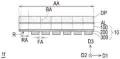
首先,在本实施例的步骤S210中,提供衬底100。在一些实施例中,衬底100的材料可包括玻璃、塑胶、陶瓷、石英、蓝宝石(sapphire)或其组合。举例而言,衬底100的材料可包括聚甲基丙烯酸甲酯(polymethyl methacrylate,PMMA)、聚碳酸酯(polycarbonate,PC)、聚酰亚胺(polyimide,PI)、聚对苯二甲酸乙二酯(polyethylene terephthalate,PET)或其他适合的材料或上述材料的组合,但本揭露不以此为限。First, in step S210 of this embodiment, a
接着,在本实施例的步骤S220中,在衬底100上形成电路层200。在一些实施例中,电路层200可包括有多条走线、接触垫、主动元件、驱动单元(例如GOP,gate on panel)或其组合。另外,在本实施例中,于衬底100上还可设置例如主动元件、驱动单元、对位标记以及电路板。举例而言,如图4A所示出,在一实施例中,于衬底100上的电路层200包含第一接触垫210、第二接触垫220、信号传输线230、第三接触垫240以及对位标记AM。第一接触垫210以及第二接触垫220可例如设置于后续欲设置振动器的区域300R中,且例如用以与此振动器电性连接,举例而言,第一接触垫210以及第二接触垫220可通过振动器具有的外部电极端子而与此振动器电性连接,但本揭露不以此为限。信号传输线230可例如与第二接触垫220以及电路板PCB电性连接,以使后续与第二接触垫220电性连接的振动器接收来自电路板PCB的信号。电路板PCB例如通过第三接触垫240与信号传输线230电性连接。在一些实施例中,电路板PCB可设置于衬底100的一侧,但本揭露不以此为限。在一些实施例中,电路板PCB可包括硬性电路板或软性电路板。举例而言,电路板PCB可为可挠性印刷电路板(flexibleprinted circuit board,FPC)。另外,电路板PCB可例如还包括有驱动晶片(未示出)以及连接器(未示出),但本揭露不以此为限。对位标记AM则例如用于使后续将形成的振动器可较精准地设置于所欲位置上。值得说明的是,一个对位标记AM可例如用于对应于一个振动器的设置处;或者一个对位标记AM可例如用于对应于一排、一列或者一个阵列的振动器的设置处,本揭露不以此为限。例如在一些实施例中,对位标记AM可应用于衬底100与显示面板DP之间的贴合对位。另外,虽然图4A示出对位标记AM具有十字形图案,但对位标记AM可具有其他形状的图案。此外,对位标记AM的材料并无特别限制,只要在辨识效果上符合所需的材料即可。Next, in step S220 of this embodiment, the
电路层200并不限于前述实施例陈述的实施例。举例而言,在另一些实施例中,如图4B所示出的电路层200的实施例,于衬底100上的电路层200可包含第一接触垫210、第二接触垫220、主动元件TFT、扫描线SL、数据线DL、共用电极线COM、对位标记AM、栅极驱动器GD以及数据驱动器DD。关于第一接触垫210、第二接触垫220、电路板PCB以及对位标记AM的技术内容可参照前述实施例,于此不再赘述。主动元件TFT例如包括有栅极G、源极S、漏极D以及半导体层SE,以用于驱动后续欲设置的振动器,其中漏极D与第二接触垫220电性连接。扫描线SL例如朝着第一方向D1延伸且与主动元件TFT中的栅极G电性连接,且数据线DL例如朝着第二方向D2延伸且与主动元件TFT中的源极S电性连接,其中第一方向D1可与第二方向D2不同,如图4B所示,第一方向D1可与第二方向D2实质垂直。另外,第一方向D1与第二方向D2可各自与衬底100的法线方向(第三方向D3)实质垂直。共用电极线COM例如朝着第一方向D1延伸且与第一接触垫210电性连接。栅极驱动器GD以及数据驱动器DD例如各自位于衬底100的第一侧与第二侧,其中第一侧可与第二侧垂直,但本揭露不以此为限。栅极驱动器GD例如与扫描线SL电性连接,且通过扫描线SL将信号传递至主动元件TFT。栅极驱动器GD例如与扫描线SL电性连接,且通过扫描线SL将相应的栅极信号传递至主动元件TFT。数据驱动器DD例如与数据线DL电性连接,且通过数据线DL将相应的数据信号传递至主动元件TFT。The
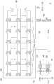
请参考图1、图5A到5E。在本实施例的步骤S230中,放置多个振动器300于衬底100上,其中多个振动器300与电路层200电性连接。多个振动器300可以阵列MxN的方式排列,例如在本实施例中,以3x6的矩阵排列,但本揭露不以此为限。另外,多个振动器300中的每一者可通过至少一个接触垫与电路层200电性连接。在本实施例中,振动器300可应用于触觉反馈或者触觉反馈与声音反馈的组合。举例而言,振动器300可包括压电元件、制动器、超音波传感器、压力传感器等构件或其组合,本揭露不以此为限。详细地说,在本实施例中,如图5A以及图5B所示出,多个振动器300可包括有外部电极端子(未示出),且多个振动器300通过该外部电极端子与设置于衬底100上的第一接触垫210以及第二接触垫220电性连接。在一些实施例中,多个振动器300与第一接触垫210以及第二接触垫220电性连接的方式可为使多个振动器300的外部电极端子与第一接触垫210以及第二接触垫220通过设置于两者之间的表面的导电胶(未示出)或于两者之间的表面进行焊锡与热压而使彼此电性连接,但本揭露不以此为限。上述导电胶的材料可包括异方性导电膜(anisotropic conductivefilm,ACF)、导电银胶、其它合适的材料或上述材料的组合,但本揭露不以此为限。另外,图5A所示出的振动器300为被动式驱动的实施例,且图5B所示出的振动器300为主动式驱动的实施例。Please refer to FIG. 1, FIGS. 5A to 5E. In step S230 of this embodiment, a plurality of
在另一些实施例中,如图5C与图5D所示出,其与图5A所示出的振动产生模块10的差异在于:于衬底100上的电路层200可还包含多个电极E,衬底100上也设置多条与电路层200电性连接的引线W。多个电极E例如朝着特定方向延伸且与信号传输线230电性连接,此特定方向(例如方向D2)可例如与信号传输线230的延伸方向(例如方向D1)实质垂直,但不限于此。多条引线W则例如设置于电路层200与多个振动器300上。在一些实施例中,多个振动器300中的每一者通过至少一条引线W与电路层200电性连接。详细地说,多条引线W设置于电路层200以及多个振动器300上,且各自与相应的电极E以及相应的振动器300电性连接,其中使电极E与振动器300电性连接的引线W在图5C与图5D中虽示出为一条,但本揭露不以此为限。基于此,振动器300可通过引线W以及电极E的设置与电路板PCB电性连接,以接受相应的信号。In some other embodiments, as shown in FIG. 5C and FIG. 5D , the difference from the
在图5E与图5F所示出的实施例中,振动产生模块10可更选择性包括第一功能层F1设置于振动器300上,使振动器300可牢固于衬底100上。其中,第一功能层F1可为如图5E所示出的非连续层,例如胶带或者为如图5F所示出的连续层,例如胶层,本揭露不以此为限。第一功能层F1还例如可具有以下实施例。在一些实施例中,第一功能层F1可例如包括高硬度特性的材料。举例而言,第一功能层F1可包括铅笔硬度大于5H的涂层(未示出)或其他合适材料,即,第一功能层F1可用作为支持层、保护层或缓冲层。在另一些实施例中,第一功能层F1可例如包括抗眩或光学匹配层的材料。光学匹配层可例如包括多个具有不同折射率的膜层,可降低在环境光的照射下,电路层干扰显示面板显示图像的问题。在又一些实施例中,第一功能层F1可包括压力感测层或压电感测层。在更一些实施例中,第一功能层F1可包括散热层。另外,在一些实施例中,第一功能层F1可包括上述的单层或多层,本揭露不以此为限。In the embodiment shown in FIG. 5E and FIG. 5F , the
然后,可选择性进行本实施例的步骤S240,测试多个振动器300中的每一者以测定多个振动器300中的每一者为合格或不合格。在将振动产生模块与显示面板贴合之前即已测试多个振动器的性能,而可减少振动器黏附以及振动器测试的次数,藉此可增加本揭露实施例的显示装置的制程效率或降低本揭露实施例的显示装置的制程成本。测试多个振动器300的方法可例如利用检测装置(如图2中的检测装置1000)对振动器300进行电性测量或振动测试,检测振动器300的性能,本揭露不以此为限。举例而言,在电性测量中利用检测电路、处理电路或其他构件来检测振动器300;或者在振动测试中,检测振动器300所产生的振动信号,或由多个振动器300所产品生的振动叠加信号,但本揭露不以此为限。在测试多个振动器300之后,若发现有不合格的振动器,则至衬底100上移除不合格的振动器,或是切断与不合格振动器之间的电性连接。Then, step S240 of this embodiment may be optionally performed to test each of the plurality of
请参考图6。由前述的制作步骤S210到S240可知,振动产生模块10至少包含了衬底100、电路层200以及多个振动器300,但不限于此。在形成了振动产生模块10之后,在本实施例的步骤S250中,将振动产生模块附接于显示面板,例如图2所示,将包含振动产生模块10的衬底100贴合至显示面板DP,藉此可减少直接将多个振动器贴附至显示面板的背面上而造成良率差及效率差的问题。在一些实施例中,衬底100与显示面板DP通过在其之间设置的黏着层AL而彼此贴合,但本揭露不以此为限。在另一些实施例中,衬底100与显示面板DP之间可通过利用静电力而彼此贴合。黏着层AL的材料可例如包括光学透明树脂(opticalclear resin;OCR)或光学透明胶(optical clear adhesive;OCA),例如包括丙烯酸系树脂、硅氧树脂、环氧树脂或其他适合的材料或上述材料的组合,但本揭露不以此为限。Please refer to Figure 6. It can be known from the aforementioned manufacturing steps S210 to S240 that the
至此,完成本揭露的显示装置的制作。值得说明的是,本实施例的显示装置的制造方法虽然是以上述方法为例进行说明;然而,本揭露的显示装置的形成方法并不以此为限。So far, the fabrication of the display device of the present disclosure is completed. It is worth noting that the method for manufacturing a display device in this embodiment is described by taking the above method as an example; however, the method for forming a display device disclosed in this disclosure is not limited thereto.
图7A为本揭露第一实施例的显示装置的剖面示意图。图7B为本揭露第二实施例的显示装置的剖面示意图。FIG. 7A is a schematic cross-sectional view of the display device according to the first embodiment of the present disclosure. 7B is a schematic cross-sectional view of a display device according to a second embodiment of the present disclosure.
请参照图7A,本实施例的显示装置1a包括显示面板DP以及振动产生模块10,其中显示面板DP与振动产生模块10之间彼此通过黏着层AL而彼此贴合。在一些实施例中,显示面板DP至少包括前述的显示单元DP1以及触控单元DP2,其中显示单元以及触控单元包括的构件及其连接关系与功能可参照前述实施例,于此不再赘述。在本实施例中,衬底100上设置有振动器300的一侧将面对显示面板DP,即,此实施例的多个振动器300设置于显示面板DP与衬底100之间,但本揭露不以此为限。本实施例的显示装置1a可还包括有偏振板PP、盖板CP以及电路板PCB’,但本揭露不以此为限。盖板CP设置于显示面板DP的电路层上,即,盖板CP与振动产生模块10设置于显示面板DP的相对侧。偏振板PP例如设置于显示面板DP与盖板CP之间。电路板PCB’例如设置于显示面板DP的至少一侧上,且可例如通过接触垫PAD与显示面板DP的电路层电性连接,但本揭露不以此为限。在一些实施例中,电路板PCB’可包括硬性电路板或软性电路板,例如可挠性印刷电路板,本揭露不以此为限。在本实施例中,电路板PCB’上可更设置有晶片TTDI(例如整合了触控与驱动功能的晶片,但不限于此)以及连接器C’。晶片TTDI例如设置于电路板PCB’上且与电路板PCB’电性连接。在一些实施例中,晶片TTDI可通过显示面板DP的电路层来控制发光元件(本实施例未示出),和/或可根据来自外界的触控信号判定触控位置并发出相应的信号。连接器C’可例如包括多个端子,外部的其他电子元件(未示出)可通过端子与电路板PCB’电性连接。在本实施例中,显示装置1a更包括驱动电路晶片DI,驱动电路晶片DI可例如设置于显示面板DP上,但本揭露不限于此。Referring to FIG. 7A , the
另外,在图7A示出的实例中,显示装置1a可选择性地更包括第二功能层F2,其中第二功能层F2设置于衬底100与多个振动器300相对的一侧上。第二功能层F2包括的材料及其功能可参照前述实施例中的第一功能层F1,本实施例不再予以赘述。在一些实施例中,第二功能层F2包括的材料及其功能可与第一功能层F1相同或类似;或者第二功能层F2包括的材料及其功能可与第一功能层F1不同。举例而言,第二功能层F2可包括散热层,本实施例不再于此赘述。在一些实施例中,显示装置1a可同时包括有设置于振动产生模块10的相对侧的第一功能层F1以及第二功能层F2,本揭露并不以此为限。In addition, in the example shown in FIG. 7A , the
振动产生模块10可例如包括衬底100、电路层200以及多个振动器300,且振动产生模块10通过与此显示面板DP电性连接而响应来自此显示面板DP的触控单元的信号。电路层200与多个振动器300例如设置于衬底100上,且多个振动器300例如与电路层200电性连接。在一些实施例中,振动产生模块10还包括电路板PCB,且电路板PCB与电路层200的其他部分可通过第三接触垫240而彼此电性连接。须说明的是,第三接触垫240可视设计而与电路层200的其他部分分别位于衬底100的同一侧或不同侧。当第三接触垫240与电路层200的其他部分不同侧时,两者可通过一通孔VH电性连接,如图7A所示。电路板PCB例如至少包括有连接器C,但本揭露不以此为限。连接器C可例如包括多个端子,与前述的连接部C’相似,外部的其他电子元件(未示出)可通过端子与电路板PCB电性连接。另外,振动产生模块10包括的其余构件及其连接关系与功能可参照前述实施例,于此不再赘述。值得一提的是,本实施例的多个振动器300与显示面板DP并未直接接触,即,多个振动器300与显示面板DP之间具有间隙G,以避免因振动器300与显示面板DP接触而影响振动器300的性能。The
如图7B所示出的显示装置1b的实施例中,衬底100上设置有振动器300的一侧背对显示面板DP,即,振动产生模块10的衬底100是设置于显示面板DP与振动产生模块10的多个振动器300之间,可减少显示装置的整体厚度。In the embodiment of the
此外,将振动产生模块10的衬底100贴合至显示面板DP之后,可进行后续工艺使振动产生模块10与显示面板DP电性连接,本揭露并未限制欲进行的后续工艺。In addition, after the
图8为本揭露第三实施例的显示装置的剖面示意图。FIG. 8 is a schematic cross-sectional view of a display device according to a third embodiment of the present disclosure.
请参照图8,其示出本实施例的显示装置1c中的显示面板DP与振动产生模块10电性连接的一种方式。如图8所示,显示面板DP包含显示区AA与非显示区NA,非显示区NA中可弯折的一部分与折叠区FA重叠,且振动产生模块10亦可弯折,当显示面板DP与振动产生模块10弯折后可彼此接触,而显示面板DP与振动产生模块10可通过设置于其上的走线(未示出)或导电胶(未示出)彼此电性连接。基于此,振动产生模块10可响应来自此显示面板DP的触控单元的信号,其例如作出振动以反馈此信号。即,本实施例的振动器300应用于触觉反馈,但本揭露不以此为限。Please refer to FIG. 8 , which shows a manner of electrical connection between the display panel DP and the
图9A为本揭露第四实施例的显示装置的剖面示意图。图9B为本揭露第四实施例的显示装置经折叠后的剖面示意图。图9C为本揭露第四实施例的显示装置的俯视示意图。FIG. 9A is a schematic cross-sectional view of a display device according to a fourth embodiment of the present disclosure. 9B is a schematic cross-sectional view of a folded display device according to a fourth embodiment of the present disclosure. FIG. 9C is a schematic top view of a display device according to a fourth embodiment of the present disclosure.
请参照图9A至图9C,其示出本揭露一实施例的显示装置1d。本实施例的显示装置1d为折叠式显示装置,即,其包括有折叠区FA并具有折叠轴BA,显示区AA与折叠区FA重叠。在本实施例中,多个振动器300不设置于折叠区FA中,以减少因显示装置1d经折叠后而损坏的机率。另外,多个振动器300(至少两个振动器)例如以阵列的方式排列,且例如沿着显示装置1d的折叠轴BA排列。详细地说,振动器300可例如为具有长边300a以及短边300b的矩形,其中振动器300的长边300a的延伸方向例如与折叠轴BA平行,但本揭露不以此为限。在其它实施例中,振动器300可为不规则形状或其它对称形状,但本揭露不以此为限。Please refer to FIG. 9A to FIG. 9C , which illustrate a
图10A为本揭露第五实施例的显示装置的剖面示意图。图10B为本揭露第五实施例的显示装置经卷起后的剖面示意图。图10C为本揭露第五实施例的显示装置的俯视示意图。FIG. 10A is a schematic cross-sectional view of a display device according to a fifth embodiment of the present disclosure. 10B is a schematic cross-sectional view of a rolled-up display device according to a fifth embodiment of the present disclosure. FIG. 10C is a schematic top view of a display device according to a fifth embodiment of the present disclosure.
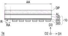
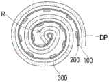
请参照图10A至图10C,其示出本揭露一实施例的显示装置1e。本实施例的显示装置1e为卷轴式显示装置,即,其包括有卷轴芯R,如图10B所是,区域RA与显示区AA的一侧重叠,当显示装置被卷成圆筒状时,区域RA可接近圆筒的中心位置,而卷轴芯R可位于区域RA中,但本揭露并不限于此。在一些实施例中,卷轴芯R的形态可例如为沿着滚动轴延伸的棒状实体卷轴,本揭露不以此为限。在本实施例中,多个振动器300不设置于卷轴芯R的区域RA中,以减少因显示装置1e被卷起时而损坏的机率。另外,多个振动器300(至少两个振动器)例如以阵列的方式排列,且例如沿着卷轴芯R的延伸方向排列。详细地说,振动器300可例如为具有长边300a以及短边300b的矩形,其中振动器300的长边300a的延伸方向例如与卷轴芯R的延伸方向平行,但本揭露不以此为限。Please refer to FIG. 10A to FIG. 10C , which illustrate a
图11A为本揭露第六实施例的显示装置的剖面示意图。图11B为本揭露第六实施例的显示装置经卷起与折叠后的剖面示意图。图11C为本揭露第六实施例的显示装置的俯视示意图。FIG. 11A is a schematic cross-sectional view of a display device according to a sixth embodiment of the present disclosure. 11B is a schematic cross-sectional view of the rolled-up and folded display device according to the sixth embodiment of the present disclosure. FIG. 11C is a schematic top view of a display device according to a sixth embodiment of the present disclosure.
请参照图11A至图11C,其示出本揭露一实施例的显示装置1f。本实施例的显示装置1f为折叠兼卷轴式(Fold'n'Roll)显示装置,即,其还包括多个折叠区FA,并具有多个折叠轴BA,更具体的说,一个折叠轴BA可位于一个折叠区FA之中。与图10A至10C的实施例相似,当显示装置被卷成筒状体时,区域RA可接近筒状体的中心位置,而卷轴芯R可位于区域RA中。卷轴芯R的形态也可为一棒状实体卷轴,但本揭露不以此为限。在本实施例中,多个振动器300不设置于折叠区FA以及卷轴芯R的区域RA中,以减少因显示装置1f被折叠或卷起时而损坏的机率。另外,多个振动器300(至少两个振动器)例如以阵列的方式排列,且例如沿着显示装置1f的折叠轴BA以及卷轴芯R的延伸方向排列。详细地说,振动器300可例如为具有长边300a以及短边300b的矩形,其中振动器300的长边300a的延伸方向例如与折叠轴BA以及卷轴芯R的延伸方向平行,但本揭露不以此为限。Please refer to FIG. 11A to FIG. 11C , which illustrate a
图12A为本揭露第七实施例的显示装置的正面示意图。图12B为本揭露第七实施例的显示装置的背面示意图。FIG. 12A is a schematic front view of a display device according to a seventh embodiment of the present disclosure. FIG. 12B is a schematic rear view of a display device according to a seventh embodiment of the present disclosure.
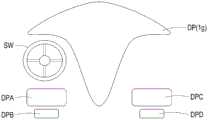
请参照图12A与图12B,其示出本揭露一实施例的显示装置1g。本实施例的显示装置1g为车用显示装置,例如可设置于仪表板(dashboard)或中控台。其具有配合车辆设计的形状。另外,也可以在车内其他位置(例如驾驶座与副驾驶座的椅背朝向后座的一面)设置显示装置,如图12A中所示的显示装置DPA、DPB、DPC、DPD。在本实施例中,振动产生模块10的衬底100的轮廓与显示面板DP类似,多个振动器300中的一部分振动器310(至少两个振动器)可沿着衬底100的边缘以在显示面板DP的背面排列。更具体的说,当振动器310沿着某元件(例如折叠轴、卷轴芯、衬底100的边缘或其它振动器)排列时,以衬底100的边缘举例,两个相邻振动器310的中心C1、C2拉出一条虚拟直线L1,而相邻两个振动器的衬底100的边缘100a与虚拟直线L1可呈现平行或是其夹角可小于或等于20度(0度≦夹角≦20度)。另外,以其它振动器举例,另外两个相邻的振动器的中心C3、C4拉出一条虚拟直线L2,则虚拟直线L1与虚拟直线L2可呈现平行或是其夹角可小于或等于20度(0度≦夹角≦20度)。Please refer to FIG. 12A and FIG. 12B , which illustrate a
在一些实施例中,显示面板DP可因其形状而具有弧形轮廓,使衬底100具有相对应的弧角R,其中尺寸较小的振动器310可设置于弧角R处,本揭露不以此为限。另外,多个振动器300中的另一部分振动器320(至少两个振动器)可沿着振动器310排列后形成的轮廓排列,即,振动器320排列后形成的轮廓与振动器310排列后形成的轮廓实质上类似,差异在于振动器320设置于较远离显示面板DP的边缘的区域。在一些实施例中,振动器310至显示面板DP的边缘的距离为振动器320至显示面板DP的边缘的距离的0.5~1倍(0.5≦距离比例<1),但本揭露不以此为限。此处欲说明的是,虽然图12B示出的振动器320排列后形成的轮廓为一个,但振动器320排列后可形成多个具有实质类似形状的轮廓。此外,多个振动器300中的又一部分振动器330(至少两个振动器)可沿着特定方向排列,该特定方向可依据例如视显示装置1g的形状决定,本揭露不以此为限。In some embodiments, the display panel DP may have an arc profile due to its shape, so that the
图13A为本揭露第八实施例的显示装置的正面示意图。图13B为本揭露第八实施例的显示装置的背面示意图。FIG. 13A is a schematic front view of a display device according to an eighth embodiment of the present disclosure. FIG. 13B is a schematic rear view of a display device according to an eighth embodiment of the present disclosure.
请参照图13A与图13B,其示出本揭露一实施例的显示装置1h。本实施例的显示装置1h亦为车用显示装置,其与显示装置1g的差异在于:振动器300分成多个组,且各组可朝着同一特定方向延伸而排列。各组的数量以及此特定方向可例如视显示装置1h的形状决定,本揭露不以此为限。另外,显示装置1h可因其形状而具有弧角R,其中尺寸较小的振动器300可设置于弧角R处,本揭露不以此为限。Please refer to FIG. 13A and FIG. 13B , which illustrate a
根据上述,本揭露实施例通过将多个振动器设置于衬底上而形成振动产生模块,并将振动产生模块与显示面板贴合,藉此可减少直接将多个振动器贴附至显示面板的背面上而造成良率差及效率差的问题。另外,本揭露实施例在将振动产生模块与显示面板贴合之前即已测试多个振动器的性能,而可减少振动器黏附以及振动器测试的次数,藉此可增加本揭露实施例的显示装置的制程效率或降低本揭露实施例的显示装置的制程成本。According to the above, the embodiments of the present disclosure form a vibration generating module by arranging a plurality of vibrators on the substrate, and attach the vibration generating module to the display panel, thereby reducing the number of directly attaching a plurality of vibrators to the display panel On the back side of the device, it causes problems of poor yield and poor efficiency. In addition, the embodiments of the present disclosure have tested the performance of multiple vibrators before attaching the vibration generating module to the display panel, which can reduce the vibrator adhesion and the number of vibrator tests, thereby increasing the display of the embodiments of the present disclosure. The process efficiency of the device may reduce the process cost of the display device of the disclosed embodiment.
最后应说明的是:以上各实施例仅用以说明本揭露的技术方案,而非对其限制;尽管参照前述各实施例对本揭露进行了详细的说明,本领域的普通技术人员应当理解:其依然可以对前述各实施例所记载的技术方案进行修改,或者对其中部分或者全部技术特征进行等同替换;而这些修改或者替换,并不使相应技术方案的本质脱离本揭露各实施例技术方案的范围。各实施例间的特征只要不违背发明精神或相冲突,均可任意混合搭配使用。Finally, it should be noted that: the above embodiments are only used to illustrate the technical solutions of the present disclosure, not to limit them; although the present disclosure has been described in detail with reference to the foregoing embodiments, those of ordinary skill in the art should understand that: It is still possible to modify the technical solutions described in the foregoing embodiments, or perform equivalent replacements for some or all of the technical features; and these modifications or replacements do not make the essence of the corresponding technical solutions deviate from the technical solutions of the various embodiments of the present disclosure. scope. As long as the features of the various embodiments do not violate the spirit of the invention or conflict, they can be mixed and matched arbitrarily.
Claims (13)
Priority Applications (4)
| Application Number | Priority Date | Filing Date | Title |
|---|---|---|---|
| CN202111327237.7ACN116110283A (en) | 2021-11-10 | 2021-11-10 | display device |
| TW111118025ATWI827053B (en) | 2021-11-10 | 2022-05-13 | Display device |
| US17/963,207US11928261B2 (en) | 2021-11-10 | 2022-10-11 | Display device |
| US18/433,439US12326977B2 (en) | 2021-11-10 | 2024-02-06 | Display device |
Applications Claiming Priority (1)
| Application Number | Priority Date | Filing Date | Title |
|---|---|---|---|
| CN202111327237.7ACN116110283A (en) | 2021-11-10 | 2021-11-10 | display device |
Publications (1)
| Publication Number | Publication Date |
|---|---|
| CN116110283Atrue CN116110283A (en) | 2023-05-12 |
Family
ID=86229471
Family Applications (1)
| Application Number | Title | Priority Date | Filing Date |
|---|---|---|---|
| CN202111327237.7APendingCN116110283A (en) | 2021-11-10 | 2021-11-10 | display device |
Country Status (3)
| Country | Link |
|---|---|
| US (2) | US11928261B2 (en) |
| CN (1) | CN116110283A (en) |
| TW (1) | TWI827053B (en) |
Cited By (1)
| Publication number | Priority date | Publication date | Assignee | Title |
|---|---|---|---|---|
| US20230262948A1 (en)* | 2022-02-15 | 2023-08-17 | Samsung Display Co., Ltd. | Emissive display device |
Families Citing this family (1)
| Publication number | Priority date | Publication date | Assignee | Title |
|---|---|---|---|---|
| GB2640158A (en)* | 2024-04-04 | 2025-10-15 | Continental Automotive Tech Gmbh | A human machine interface and a method of operating the same |
Citations (7)
| Publication number | Priority date | Publication date | Assignee | Title |
|---|---|---|---|---|
| TW201101137A (en)* | 2009-06-29 | 2011-01-01 | J Touch Corp | Touch panel with matrix type tactile feedback |
| CN203057505U (en)* | 2012-12-13 | 2013-07-10 | 瑞声声学科技(常州)有限公司 | Piezoelectric Ceramic Array Thin Film |
| CN104771190A (en)* | 2014-01-14 | 2015-07-15 | 精工爱普生株式会社 | Ultrasonic device, ultrasonic transducer device, electronic device and ultrasonic imaging device |
| US20200059733A1 (en)* | 2018-08-20 | 2020-02-20 | Lg Display Co., Ltd. | Display apparatus including flexible vibration module and method of manufacturing the flexible vibration module |
| CN111381672A (en)* | 2018-12-31 | 2020-07-07 | 乐金显示有限公司 | Vibration generating device and display apparatus including the same |
| US20200401227A1 (en)* | 2019-06-19 | 2020-12-24 | Samsung Display Co., Ltd. | Display device and method of driving the same |
| CN112346592A (en)* | 2019-08-09 | 2021-02-09 | 三星显示有限公司 | Display device |
Family Cites Families (6)
| Publication number | Priority date | Publication date | Assignee | Title |
|---|---|---|---|---|
| TWI514347B (en)* | 2006-09-29 | 2015-12-21 | Semiconductor Energy Lab | Display device and electronic device |
| KR102229137B1 (en) | 2014-05-20 | 2021-03-18 | 삼성디스플레이 주식회사 | Display apparatus |
| KR102589751B1 (en)* | 2016-07-26 | 2023-10-17 | 삼성디스플레이 주식회사 | Display device |
| KR102552930B1 (en)* | 2018-06-27 | 2023-07-07 | 삼성디스플레이 주식회사 | Panel bottom member and display device including the same |
| KR102765540B1 (en)* | 2019-03-14 | 2025-02-12 | 삼성전자주식회사 | Electronic device including haptic actuator |
| KR102821789B1 (en)* | 2019-09-30 | 2025-06-17 | 삼성전자주식회사 | Electronic device including haptic actuator |
- 2021
- 2021-11-10CNCN202111327237.7Apatent/CN116110283A/enactivePending
- 2022
- 2022-05-13TWTW111118025Apatent/TWI827053B/enactive
- 2022-10-11USUS17/963,207patent/US11928261B2/enactiveActive
- 2024
- 2024-02-06USUS18/433,439patent/US12326977B2/enactiveActive
Patent Citations (7)
| Publication number | Priority date | Publication date | Assignee | Title |
|---|---|---|---|---|
| TW201101137A (en)* | 2009-06-29 | 2011-01-01 | J Touch Corp | Touch panel with matrix type tactile feedback |
| CN203057505U (en)* | 2012-12-13 | 2013-07-10 | 瑞声声学科技(常州)有限公司 | Piezoelectric Ceramic Array Thin Film |
| CN104771190A (en)* | 2014-01-14 | 2015-07-15 | 精工爱普生株式会社 | Ultrasonic device, ultrasonic transducer device, electronic device and ultrasonic imaging device |
| US20200059733A1 (en)* | 2018-08-20 | 2020-02-20 | Lg Display Co., Ltd. | Display apparatus including flexible vibration module and method of manufacturing the flexible vibration module |
| CN111381672A (en)* | 2018-12-31 | 2020-07-07 | 乐金显示有限公司 | Vibration generating device and display apparatus including the same |
| US20200401227A1 (en)* | 2019-06-19 | 2020-12-24 | Samsung Display Co., Ltd. | Display device and method of driving the same |
| CN112346592A (en)* | 2019-08-09 | 2021-02-09 | 三星显示有限公司 | Display device |
Cited By (1)
| Publication number | Priority date | Publication date | Assignee | Title |
|---|---|---|---|---|
| US20230262948A1 (en)* | 2022-02-15 | 2023-08-17 | Samsung Display Co., Ltd. | Emissive display device |
Also Published As
| Publication number | Publication date |
|---|---|
| US20240211048A1 (en) | 2024-06-27 |
| TW202320373A (en) | 2023-05-16 |
| US20230146224A1 (en) | 2023-05-11 |
| US11928261B2 (en) | 2024-03-12 |
| TWI827053B (en) | 2023-12-21 |
| US12326977B2 (en) | 2025-06-10 |
Similar Documents
| Publication | Publication Date | Title |
|---|---|---|
| US10969832B2 (en) | Display device | |
| CN107015694B (en) | Display device | |
| US12326977B2 (en) | Display device | |
| CN109597516B (en) | display screen | |
| CN110531883B (en) | display device | |
| CN112987957B (en) | electronic devices | |
| US11067723B2 (en) | Optical touch film, display device including the same, and manufacturing method thereof | |
| CN107037917A (en) | Collapsible display | |
| US12245457B2 (en) | Display device layer aligned with display panel and display device having the same | |
| CN117412628A (en) | Flexible display device | |
| CN113066820A (en) | display device | |
| US11816281B2 (en) | Display device with input sensor having alignment member connected to ground | |
| CN114823795A (en) | Display device | |
| CN110703936B (en) | Display device | |
| CN101359106A (en) | Display panel and application thereof | |
| US12193180B2 (en) | Electronic device | |
| US20250040371A1 (en) | Display device and method of fabricating the same | |
| TW202405633A (en) | Touch device | |
| TW202301008A (en) | Electronic device | |
| CN119493491A (en) | Touch sensor and display device | |
| CN114973939A (en) | Display device | |
| CN119866139A (en) | Organic light emitting display device |
Legal Events
| Date | Code | Title | Description |
|---|---|---|---|
| PB01 | Publication | ||
| PB01 | Publication | ||
| SE01 | Entry into force of request for substantive examination | ||
| SE01 | Entry into force of request for substantive examination |