CN116096071A - Semiconductor structure and preparation method thereof - Google Patents
Semiconductor structure and preparation method thereofDownload PDFInfo
- Publication number
- CN116096071A CN116096071ACN202111298101.8ACN202111298101ACN116096071ACN 116096071 ACN116096071 ACN 116096071ACN 202111298101 ACN202111298101 ACN 202111298101ACN 116096071 ACN116096071 ACN 116096071A
- Authority
- CN
- China
- Prior art keywords
- mask layer
- layer
- pattern
- etching
- capacitor
- Prior art date
- Legal status (The legal status is an assumption and is not a legal conclusion. Google has not performed a legal analysis and makes no representation as to the accuracy of the status listed.)
- Granted
Links
Images


Classifications
- H—ELECTRICITY
- H01—ELECTRIC ELEMENTS
- H01L—SEMICONDUCTOR DEVICES NOT COVERED BY CLASS H10
- H01L21/00—Processes or apparatus adapted for the manufacture or treatment of semiconductor or solid state devices or of parts thereof
- H01L21/02—Manufacture or treatment of semiconductor devices or of parts thereof
- H01L21/04—Manufacture or treatment of semiconductor devices or of parts thereof the devices having potential barriers, e.g. a PN junction, depletion layer or carrier concentration layer
- H01L21/18—Manufacture or treatment of semiconductor devices or of parts thereof the devices having potential barriers, e.g. a PN junction, depletion layer or carrier concentration layer the devices having semiconductor bodies comprising elements of Group IV of the Periodic Table or AIIIBV compounds with or without impurities, e.g. doping materials
- H01L21/30—Treatment of semiconductor bodies using processes or apparatus not provided for in groups H01L21/20 - H01L21/26
- H01L21/302—Treatment of semiconductor bodies using processes or apparatus not provided for in groups H01L21/20 - H01L21/26 to change their surface-physical characteristics or shape, e.g. etching, polishing, cutting
- H01L21/306—Chemical or electrical treatment, e.g. electrolytic etching
- H01L21/3065—Plasma etching; Reactive-ion etching
- H—ELECTRICITY
- H10—SEMICONDUCTOR DEVICES; ELECTRIC SOLID-STATE DEVICES NOT OTHERWISE PROVIDED FOR
- H10B—ELECTRONIC MEMORY DEVICES
- H10B12/00—Dynamic random access memory [DRAM] devices
Landscapes
- Engineering & Computer Science (AREA)
- Physics & Mathematics (AREA)
- Plasma & Fusion (AREA)
- Condensed Matter Physics & Semiconductors (AREA)
- General Physics & Mathematics (AREA)
- Manufacturing & Machinery (AREA)
- Computer Hardware Design (AREA)
- Microelectronics & Electronic Packaging (AREA)
- Power Engineering (AREA)
- Semiconductor Integrated Circuits (AREA)
Abstract
Translated fromChinese
Description
Translated fromChinese技术领域technical field
本申请涉及半导体技术领域,涉及但不限于一种半导体结构及其制备方法。The present application relates to the field of semiconductor technology, and relates to but not limited to a semiconductor structure and a preparation method thereof.
背景技术Background technique
动态随机存取存储器(Dynamic Random Access Memory,DRAM)包含由多个存储单元构成的阵列区域(Array area)以及控制电路所在的外围区域(Peripheral area)。随着半导体存储技术的快速发展,市场对半导体存储产品的存储能力提出了更高的要求,对于动态随机存储器来说,存储电容的分布密度及单个电容的存储电量制约着电容存储器的存储能力及稳定性。Dynamic Random Access Memory (DRAM) includes an array area (Array area) composed of multiple memory cells and a peripheral area (Peripheral area) where the control circuit is located. With the rapid development of semiconductor storage technology, the market has put forward higher requirements for the storage capacity of semiconductor storage products. For DRAM, the distribution density of storage capacitors and the storage power of a single capacitor restrict the storage capacity and stability.
发明内容Contents of the invention
有鉴于此,本申请实施例提供一种半导体结构及其制备方法。In view of this, embodiments of the present application provide a semiconductor structure and a manufacturing method thereof.
第一方面,本申请实施例提供一种半导体结构的制备方法,包括:In a first aspect, an embodiment of the present application provides a method for preparing a semiconductor structure, including:
在具有阵列区域和外围区域的基底上形成叠层结构;forming a laminated structure on a substrate having an array region and a peripheral region;
在所述叠层结构上形成第一掩膜层;其中,对应于所述阵列区域的所述第一掩膜层具有第一图案;forming a first mask layer on the stacked structure; wherein, the first mask layer corresponding to the array region has a first pattern;
对所述阵列区域上的第一掩膜层进行离子掺杂,得到掺杂后的第一掩膜层;performing ion doping on the first mask layer on the array region to obtain a doped first mask layer;
通过所述掺杂后的第一掩膜层刻蚀所述叠层结构,以将所述第一图案转移至所述叠层结构中。The stacked structure is etched through the doped first mask layer to transfer the first pattern into the stacked structure.
在一些实施例中,在所述叠层结构上形成第一掩膜层,包括:In some embodiments, forming a first mask layer on the laminated structure includes:
在所述叠层结构上依次形成第一初始掩膜层和第二初始掩膜层;其中,所述第二初始掩膜层中形成有所述第一图案;A first initial mask layer and a second initial mask layer are sequentially formed on the laminated structure; wherein, the first pattern is formed in the second initial mask layer;
通过所述第二初始掩膜层刻蚀所述第一初始掩膜层,以实现将所述第一图案转移至所述第一初始掩膜层中,形成所述第一掩膜层;etching the first initial mask layer through the second initial mask layer, so as to transfer the first pattern into the first initial mask layer, and form the first mask layer;
其中,所述第一掩膜层暴露出部分叠层结构的表面。Wherein, the first mask layer exposes part of the surface of the laminated structure.
在一些实施例中,所述方法还包括:In some embodiments, the method also includes:
在形成所述第一掩膜层之后,去除所述第二初始掩膜层。After forming the first mask layer, the second initial mask layer is removed.
在一些实施例中,所述对所述阵列区域上的第一掩膜层进行离子掺杂,得到掺杂后的第一掩膜层,包括:In some embodiments, performing ion doping on the first mask layer on the array region to obtain a doped first mask layer includes:
在所述第一掩膜层和所述部分叠层结构上沉积牺牲层;depositing a sacrificial layer on the first mask layer and the partial stack structure;
刻蚀所述阵列区域上的所述牺牲层,以暴露出所述阵列区域上的部分所述第一掩膜层;etching the sacrificial layer on the array area to expose part of the first mask layer on the array area;
对暴露出的所述第一掩膜层进行离子掺杂,得到掺杂后的第一掩膜层。Ion doping is performed on the exposed first mask layer to obtain a doped first mask layer.
在一些实施例中,所述刻蚀所述阵列区域上的所述牺牲层,以暴露出所述阵列区域上的部分所述第一掩膜层,包括:In some embodiments, the etching the sacrificial layer on the array region to expose part of the first mask layer on the array region includes:
在所述牺牲层上形成第二掩膜层;forming a second mask layer on the sacrificial layer;
图形化所述第二掩膜层,暴露出对应于所述阵列区域的所述牺牲层;patterning the second mask layer to expose the sacrificial layer corresponding to the array area;
刻蚀去除部分暴露的所述牺牲层,以暴露出部分所述第一掩膜层。Etching and removing part of the exposed sacrificial layer to expose part of the first mask layer.
在一些实施例中,所述方法还包括:In some embodiments, the method also includes:
在对暴露出的所述第一掩膜层进行离子掺杂之后,去除所述外围区域上的第二掩膜层和剩余的所述牺牲层,暴露出所述外围区域上的第一掩膜层。After ion doping the exposed first mask layer, removing the second mask layer on the peripheral region and the remaining sacrificial layer, exposing the first mask layer on the peripheral region layer.
在一些实施例中,所述掺杂后的第一掩膜层与所述叠层结构之间的刻蚀选择比大于所述第一掩膜层与所述叠层结构之间的刻蚀选择比。In some embodiments, the etching selectivity between the doped first mask layer and the stacked structure is greater than the etching selectivity between the first mask layer and the stacked structure Compare.
在一些实施例中,对应于所述外围区域的所述第一掩膜层具有第二图案,所述第二图案的图案密度小于所述第一图案的图案密度。In some embodiments, the first mask layer corresponding to the peripheral region has a second pattern having a pattern density less than that of the first pattern.
在一些实施例中,所述第一图案为电容孔图案,且所述基底中形成有与所述电容孔图案相对应的接触结构。In some embodiments, the first pattern is a capacitor hole pattern, and a contact structure corresponding to the capacitor hole pattern is formed in the substrate.
在一些实施例中,所述叠层结构包括由下至上依次堆叠的第一牺牲层、第一支撑层、第二牺牲层和第二支撑层。In some embodiments, the stacked structure includes a first sacrificial layer, a first supporting layer, a second sacrificial layer and a second supporting layer stacked sequentially from bottom to top.
在一些实施例中,所述通过所述掺杂后的第一掩膜层刻蚀所述叠层结构,以将所述第一图案转移至所述叠层结构中,包括:In some embodiments, the etching the stacked structure through the doped first mask layer to transfer the first pattern into the stacked structure includes:
通过所述掺杂后的第一掩膜层,依次刻蚀所述第二支撑层、所述第二牺牲层、所述第一支撑层和所述第一牺牲层,以将所述电容孔图案转移至所述叠层结构中,在所述叠层结构中形成多个电容孔和位于相邻两个电容孔之间的刻蚀柱;Through the doped first mask layer, etch the second supporting layer, the second sacrificial layer, the first supporting layer and the first sacrificial layer in sequence, so that the capacitance hole The pattern is transferred to the stacked structure, and a plurality of capacitor holes and etching columns between two adjacent capacitor holes are formed in the stacked structure;
其中,所述电容孔暴露出部分所述接触结构。Wherein, the capacitor hole exposes part of the contact structure.
在一些实施例中,所述方法还包括:In some embodiments, the method also includes:
在形成所述电容孔之后,去除所述第一掩膜层。After the capacitor hole is formed, the first mask layer is removed.
在一些实施例中,所述方法还包括:In some embodiments, the method also includes:
处理所述刻蚀柱,形成电容结构。The etched pillars are processed to form capacitor structures.
在一些实施例中,所述处理所述刻蚀柱,形成电容结构,包括:In some embodiments, the processing the etched pillar to form a capacitor structure includes:
在所述电容孔的内壁和所述刻蚀柱的表面形成第一电极层;forming a first electrode layer on the inner wall of the capacitor hole and the surface of the etched pillar;
在所述第二支撑层中形成第一开口;forming a first opening in the second support layer;
通过所述第一开口去除所述第二牺牲层;removing the second sacrificial layer through the first opening;
在所述第一支撑层中形成第二开口;forming a second opening in the first support layer;
通过所述第二开口去除所述第一牺牲层。The first sacrificial layer is removed through the second opening.
在所述第一电极层的表面依次沉积电介质层和第二电极层,形成所述电容结构。A dielectric layer and a second electrode layer are sequentially deposited on the surface of the first electrode layer to form the capacitance structure.
第二方面,本申请实施例提供一种半导体结构,所述半导体结构通过上述半导体结构制备方法制备,所述半导体结构至少包括:基底和电容结构;In a second aspect, an embodiment of the present application provides a semiconductor structure, the semiconductor structure is prepared by the above semiconductor structure preparation method, and the semiconductor structure at least includes: a substrate and a capacitor structure;
其中,所述基底包括接触结构;Wherein, the substrate includes a contact structure;
所述电容结构位于所述基底的表面,且所述电容结构与所述接触结构相接触。The capacitive structure is located on the surface of the substrate, and the capacitive structure is in contact with the contact structure.
本申请实施例提供的半导体结构及其制备方法,其中,半导体结构的制备方法包括:在具有阵列区域和外围区域的基底上形成叠层结构;在叠层结构上形成第一掩膜层;对应于阵列区域的第一掩膜层具有第一图案;对阵列区域上的第一掩膜层进行离子掺杂,得到掺杂后的第一掩膜层;通过掺杂后的第一掩膜层刻蚀叠层结构,以将第一图案转移至叠层结构中。本申请实施例中,通过对阵列区域上的第一掩膜层进行掺杂,使得阵列区域上的第一掩膜层与外围区域上的第一掩膜层具有不同的刻蚀选择比,如此,可以抵消不同区域上的第一掩膜层在刻蚀过程中所带来的刻蚀负载效应,进而可以提高电容图案的完整性和所形成的电容结构的容量。The semiconductor structure and its preparation method provided in the embodiments of the present application, wherein, the preparation method of the semiconductor structure includes: forming a stacked structure on a substrate having an array region and a peripheral region; forming a first mask layer on the stacked structure; corresponding The first mask layer on the array area has a first pattern; ion doping is performed on the first mask layer on the array area to obtain a doped first mask layer; The stacked structure is etched to transfer the first pattern into the stacked structure. In the embodiment of the present application, by doping the first mask layer on the array region, the first mask layer on the array region and the first mask layer on the peripheral region have different etching selectivity ratios, thus , the etching load effect brought by the first mask layer on different regions during the etching process can be offset, thereby improving the integrity of the capacitance pattern and the capacity of the formed capacitance structure.
附图说明Description of drawings
在附图(其不一定是按比例绘制的)中,相似的附图标记可在不同的视图中描述相似的部件。具有不同字母后缀的相似附图标记可表示相似部件的不同示例。附图以示例而非限制的方式大体示出了本文中所讨论的各个实施例。In the drawings (which are not necessarily drawn to scale), like reference numerals may describe like parts in different views. Similar reference numbers with different letter suffixes may indicate different instances of similar components. The drawings generally illustrate the various embodiments discussed herein, by way of example and not limitation.
图1a~1c为本申请一个实施例提供的半导体结构形成过程的结构示意图;Figures 1a-1c are structural schematic diagrams of the process of forming a semiconductor structure provided by an embodiment of the present application;
图2为本申请另一个实施例提供的半导体结构的制备方法的一种结构示意图;FIG. 2 is a schematic structural diagram of a method for preparing a semiconductor structure provided in another embodiment of the present application;
图3a~3n为本申请一个实施例提供的半导体结构制备过程的结构示意图;3a-3n are structural schematic diagrams of the semiconductor structure preparation process provided by an embodiment of the present application;
图4为本申请一个实施例提供的半导体结构的一种剖面图;FIG. 4 is a cross-sectional view of a semiconductor structure provided by an embodiment of the present application;
附图标记说明:Explanation of reference signs:
100/200-基底;101/201-叠层结构;102-第一硬掩膜层;103-第二硬掩膜层;101-1/B-外围区域;100-2/A-阵列区域;102a-第一次刻蚀后的第一硬掩膜层;102b-第二次刻蚀后的第一硬掩膜层;101a-电容图形;201a-第一牺牲层;201b/213-第一支撑层;201c-第二牺牲层;201d/214-第二支撑层;200a-接触结构;200b-绝缘层;202a-第一初始掩膜层;203a-第二初始掩膜层;202-第一掩膜层;202b-掺杂后的第一掩膜层;204-牺牲层;205-第二掩膜层;205a-介电抗反射涂层;205b-底部抗反射涂层;205c-光刻胶层;206c-图形化的光刻胶层;206b-图形化的底部抗反射涂层;206a-图形化的介电抗反射涂层;204a-部分牺牲层;207-电容孔;208-刻蚀柱;209-第一电极层;210-电介质层;211-第二电极层;212-导电材料;40-半导体结构;D-第一开口;E-第二开口。100/200-substrate; 101/201-stack structure; 102-first hard mask layer; 103-second hard mask layer; 101-1/B-peripheral area; 100-2/A-array area; 102a-the first hard mask layer after the first etching; 102b-the first hard mask layer after the second etching; 101a-capacitor pattern; 201a-the first sacrificial layer; 201b/213-the first 201c-second sacrificial layer; 201d/214-second supporting layer; 200a-contact structure; 200b-insulating layer; 202a-first initial mask layer; 203a-second initial mask layer; 202-first A mask layer; 202b-doped first mask layer; 204-sacrifice layer; 205-second mask layer; 205a-dielectric anti-reflection coating; 205b-bottom anti-reflection coating; 205c-light Resist layer; 206c-patterned photoresist layer; 206b-patterned bottom antireflective coating; 206a-patterned dielectric antireflective coating; 204a-partial sacrificial layer; 207-capacitor hole; 208- 209-first electrode layer; 210-dielectric layer; 211-second electrode layer; 212-conductive material; 40-semiconductor structure; D-first opening; E-second opening.
具体实施方式Detailed ways
下面将参照附图更详细地描述本申请公开的示例性实施方式。虽然附图中显示了本申请的示例性实施方式,然而应当理解,可以以各种形式实现本申请,而不应被这里阐述的具体实施方式所限制。相反,提供这些实施方式是为了能够更透彻地理解本申请,并且能够将本申请公开的范围完整的传达给本领域的技术人员。Exemplary embodiments disclosed in the present application will be described in more detail below with reference to the accompanying drawings. Although exemplary embodiments of the present application are shown in the drawings, it should be understood that the present application may be embodied in various forms and should not be limited to the specific embodiments set forth herein. Rather, these embodiments are provided for a more thorough understanding of the present application and for fully conveying the scope disclosed in the present application to those skilled in the art.
在下文的描述中,给出了大量具体的细节以便提供对本申请更为彻底的理解。然而,对于本领域技术人员而言显而易见的是,本申请可以无需一个或多个这些细节而得以实施。在其他的例子中,为了避免与本申请发生混淆,对于本领域公知的一些技术特征未进行描述;即,这里不描述实际实施例的全部特征,不详细描述公知的功能和结构。In the following description, numerous specific details are given in order to provide a more thorough understanding of the present application. It will be apparent, however, to one skilled in the art that the present application may be practiced without one or more of these details. In other examples, in order to avoid confusion with the present application, some technical features known in the art are not described; that is, all features of the actual embodiment are not described here, and well-known functions and structures are not described in detail.
在附图中,为了清楚,层、区、元件的尺寸以及其相对尺寸可能被夸大。自始至终相同附图标记表示相同的元件。In the drawings, the size of layers, regions, elements and their relative sizes may be exaggerated for clarity. Like reference numerals refer to like elements throughout.
应当明白,当元件或层被称为“在……上”、“与……相邻”、“连接到”或“耦合到”其它元件或层时,其可以直接地在其它元件或层上、与之相邻、连接或耦合到其它元件或层,或者可以存在居间的元件或层。相反,当元件被称为“直接在……上”、“与……直接相邻”、“直接连接到”或“直接耦合到”其它元件或层时,则不存在居间的元件或层。应当明白,尽管可使用术语第一、第二、第三等描述各种元件、部件、区、层和/或部分,这些元件、部件、区、层和/或部分不应当被这些术语限制。这些术语仅仅用来区分一个元件、部件、区、层或部分与另一个元件、部件、区、层或部分。因此,在不脱离本申请教导之下,下面讨论的第一元件、部件、区、层或部分可表示为第二元件、部件、区、层或部分。而当讨论的第二元件、部件、区、层或部分时,并不表明本申请必然存在第一元件、部件、区、层或部分。It will be understood that when an element or layer is referred to as being "on," "adjacent to," "connected to" or "coupled to" another element or layer, it can be directly on the other element or layer. , adjacent to, connected to, or coupled to other elements or layers, or intervening elements or layers may be present. In contrast, when an element is referred to as being "directly on," "directly adjacent to," "directly connected to" or "directly coupled to" another element or layer, there are no intervening elements or layers present. It will be understood that, although the terms first, second, third etc. may be used to describe various elements, components, regions, layers and/or sections, these elements, components, regions, layers and/or sections should not be limited by these terms. These terms are only used to distinguish one element, component, region, layer or section from another element, component, region, layer or section. Thus, a first element, component, region, layer or section discussed below could be termed a second element, component, region, layer or section without departing from the teachings of the present application. When a second element, component, region, layer or section is discussed, it does not necessarily indicate that the present application must have a first element, component, region, layer or section.
在此使用的术语的目的仅在于描述具体实施例并且不作为本申请的限制。在此使用时,单数形式的“一”、“一个”和“所述/该”也意图包括复数形式,除非上下文清楚指出另外的方式。还应明白术语“组成”和/或“包括”,当在该说明书中使用时,确定所述特征、整数、步骤、操作、元件和/或部件的存在,但不排除一个或更多其它的特征、整数、步骤、操作、元件、部件和/或组的存在或添加。在此使用时,术语“和/或”包括相关所列项目的任何及所有组合。The terminology used herein is for the purpose of describing particular embodiments only and is not intended to be limiting of the application. As used herein, the singular forms "a", "an" and "the/the" are intended to include the plural forms as well, unless the context clearly dictates otherwise. It should also be understood that the terms "consists of" and/or "comprising", when used in this specification, identify the presence of stated features, integers, steps, operations, elements and/or parts, but do not exclude one or more other Presence or addition of features, integers, steps, operations, elements, parts and/or groups. As used herein, the term "and/or" includes any and all combinations of the associated listed items.
在详细介绍本申请实施例提供的半导体结构的形成方法之前,首先对相关技术中半导体结构的形成过程进行说明。Before introducing the method for forming the semiconductor structure provided in the embodiment of the present application in detail, the process of forming the semiconductor structure in the related art will be described first.
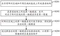
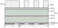
图1a~1c为本申请一个实施例提供的半导体结构形成过程的结构示意图,如图1a所示,在基底100的表面形成叠层结构101,并且在叠层结构101的表面形成第一硬掩膜层102和第二硬掩膜层103,其中,第二硬掩膜层103中具有形成电容孔的图案。基底100包括外围区域100-1和阵列区域100-2,其中,阵列区域100-2上的第二硬掩膜层中的电容孔图案的图案密度大于外围区域100-1上的第二硬掩膜层中的电容孔图案的图案密度。1a-1c are structural schematic diagrams of the semiconductor structure formation process provided by an embodiment of the present application. As shown in FIG. The
半导体结构的形成过程包括两次图案转移过程,第一次图案转移过程是:通过第二硬掩膜层刻蚀第一硬掩膜层,以实现将第二硬掩膜层中的电容孔图案转移至第一硬掩膜层中。如图1b所示,第一次图案转移得到了第一次刻蚀后的第一硬掩膜层102a。在第一次图案转移过程中,由于刻蚀负载效应,位于阵列区域100-2上的第二硬掩膜层103的厚度t1,小于位于外围区域100-1上第二硬掩膜层103的厚度t2。第二次图案转移过程是:通过第一次刻蚀后的第一硬掩膜层102a刻蚀叠层结构101,以实现将电容孔图案转移至叠层结构101中;在进行第二次图案转移之前,需要去除第二硬掩膜层103。如图1c所示,第二次图案转移过程形成电容图形101a和第二次刻蚀后的第一硬掩膜层102b,其中,电容图形(Bar)101a具有顶部尺寸B和高度D,且相邻两个电容图形之间的距离为S。在去除第二硬掩膜层103和第二次图案转移过程中,由于刻蚀负载效应,位于阵列区域100-2上的第一硬掩膜层的厚度t3,小于位于外围区域100-1上第一硬掩膜层的厚度t4,且阵列区域100-2上的第一硬掩膜层与位于外围区域100-1上的第一硬掩膜层具有不同的粗糙度。The forming process of the semiconductor structure includes two pattern transfer processes, the first pattern transfer process is: etching the first hard mask layer through the second hard mask layer, so as to realize the capacitance hole pattern in the second hard mask layer into the first hard mask layer. As shown in FIG. 1b, the first pattern transfer obtains the first
在将电容孔图案转移至叠层结构中后,还需要去除上述第二次刻蚀后的第一硬掩膜层102b。After the capacitor hole pattern is transferred to the stacked structure, the first
本申请的另一个实施例提供了一种半导体结构及其制备方法,其中,半导体结构的制备方法包括:在具有阵列区域和外围区域的基底上形成叠层结构;在叠层结构上形成第一掩膜层;对应于阵列区域的第一掩膜层具有第一图案;对阵列区域上的第一掩膜层进行离子掺杂,得到掺杂后的第一掩膜层;通过掺杂后的第一掩膜层刻蚀叠层结构,以将第一图案转移至叠层结构中。本申请实施例中,通过对阵列区域上的第一掩膜层进行掺杂,使得阵列区域上的第一掩膜层与外围区域上的第一掩膜层具有不同的刻蚀选择比,如此,可以抵消不同区域上的第一掩膜层在刻蚀过程中所带来的刻蚀负载效应,进而可以提高电容图案的完整性和所形成的电容结构的容量。Another embodiment of the present application provides a semiconductor structure and a manufacturing method thereof, wherein the manufacturing method of the semiconductor structure includes: forming a stacked structure on a substrate having an array region and a peripheral region; forming a first stacked structure on the stacked structure Mask layer; the first mask layer corresponding to the array area has a first pattern; ion doping is performed on the first mask layer on the array area to obtain a doped first mask layer; through the doped The first mask layer etches the stacked structure to transfer the first pattern into the stacked structure. In the embodiment of the present application, by doping the first mask layer on the array region, the first mask layer on the array region and the first mask layer on the peripheral region have different etching selectivity ratios, thus , the etching load effect brought by the first mask layer on different regions during the etching process can be offset, thereby improving the integrity of the capacitance pattern and the capacity of the formed capacitance structure.
图2为本申请另一个实施例提供的半导体结构的制备方法的一种结构示意图,如图2所示,包括以下步骤:Fig. 2 is a schematic structural diagram of a method for preparing a semiconductor structure provided in another embodiment of the present application, as shown in Fig. 2 , including the following steps:
步骤S201、在具有阵列区域和外围区域的基底上形成叠层结构。Step S201 , forming a laminated structure on a substrate having an array area and a peripheral area.
叠层结构用于形成电容结构,叠层结构包括由下至上依次堆叠的第一牺牲层、第一支撑层、第二牺牲层和第二支撑层。其中,第一牺牲层和第二牺牲层可以是氧化物层,例如氧化硅层;第一支撑层和第二支撑层可以是氮化硅层。The stacked structure is used to form a capacitor structure, and the stacked structure includes a first sacrificial layer, a first supporting layer, a second sacrificial layer and a second supporting layer stacked in sequence from bottom to top. Wherein, the first sacrificial layer and the second sacrificial layer may be oxide layers, such as silicon oxide layers; the first supporting layer and the second supporting layer may be silicon nitride layers.
基底包括阵列区域和外围区域,阵列区域用于形成半导体存储单元的存储器件,例如,存储电容;外围区域用于形成外围控制电路。The substrate includes an array area and a peripheral area. The array area is used to form a storage device of the semiconductor memory unit, for example, a storage capacitor; the peripheral area is used to form a peripheral control circuit.
本申请实施例中,基底至少包括接触结构,接触结构用于与形成的电容结构电连接。本申请实施例中,接触结构的材料可以是任意一种导电材料,例如,钨(W)、钴(Co)、铜(Cu)、铝(Al)、多晶硅、掺杂硅、硅化物或其任何组合。In the embodiment of the present application, the substrate at least includes a contact structure, and the contact structure is used to electrically connect with the formed capacitor structure. In the embodiment of the present application, the material of the contact structure can be any conductive material, for example, tungsten (W), cobalt (Co), copper (Cu), aluminum (Al), polysilicon, doped silicon, silicide or any combination.
在其它实施例中,基底还可以包括半导体衬底、位于半导体衬底内部字线结构、位于半导体衬底表面的位线结构和覆盖接触结构的绝缘层。半导体衬底的材料可以选择硅(Si)、硅锗合金(SiGe)、碳化硅(SiC)、氧化铝(Al2O3)、氮化铝(AlN)、氧化锌(ZnO)、氧化镓(Ga2O3)或铝酸锂(LiAlO2)等中的任意一种。In other embodiments, the base may further include a semiconductor substrate, a word line structure inside the semiconductor substrate, a bit line structure on the surface of the semiconductor substrate, and an insulating layer covering the contact structure. The material of the semiconductor substrate can be selected from silicon (Si), silicon germanium alloy (SiGe), silicon carbide (SiC), aluminum oxide (Al2 O3 ), aluminum nitride (AlN), zinc oxide (ZnO), gallium oxide ( any of Ga2 O3 ), lithium aluminate (LiAlO2 ), and the like.
步骤S202、在叠层结构上形成第一掩膜层;其中,对应于阵列区域的第一掩膜层具有第一图案。Step S202 , forming a first mask layer on the stacked structure; wherein, the first mask layer corresponding to the array area has a first pattern.
本申请实施例中,第一掩膜层可以是任意一种硬掩膜层,例如,多晶硅层、氮化硅层或者旋涂碳层。第一图案可以为电容孔图案或者其它图案。In the embodiment of the present application, the first mask layer may be any hard mask layer, for example, a polysilicon layer, a silicon nitride layer, or a spin-on-carbon layer. The first pattern may be a capacitor hole pattern or other patterns.
在一些实施例中,对应于外围区域的第一掩膜层具有第二图案,第二图也可以为电容孔图案或者其它图案。In some embodiments, the first mask layer corresponding to the peripheral region has a second pattern, and the second pattern may also be a capacitance hole pattern or other patterns.
需要说明的是,本申请实施例中,第二图案的图案密度小于第一图案的图案密度。It should be noted that, in the embodiment of the present application, the pattern density of the second pattern is smaller than the pattern density of the first pattern.
步骤S203、对阵列区域上的第一掩膜层进行离子掺杂,得到掺杂后的第一掩膜层。Step S203 , performing ion doping on the first mask layer on the array area to obtain a doped first mask layer.
本申请实施例中,对阵列区域上的第一掩膜层进行掺杂的离子可以是任意一种能够使得第一掩膜层的刻蚀难度加大的离子,例如,P型离子或其他类型的离子,如此,阵列区域上的第一掩膜层和外围区域上的第一掩膜层会具有不同的刻蚀选择比。In the embodiment of the present application, the ions that dope the first mask layer on the array region can be any kind of ions that can make the etching of the first mask layer more difficult, for example, P-type ions or other types of ions. In this way, the first mask layer on the array area and the first mask layer on the peripheral area will have different etching selectivity ratios.
步骤S204、通过掺杂后的第一掩膜层刻蚀叠层结构,以将第一图案转移至叠层结构中。Step S204 , etching the stacked structure through the doped first mask layer, so as to transfer the first pattern into the stacked structure.
图3a~3n为本申请一个实施例提供的半导体结构制备过程的结构示意图,接下来请参考图3a~3n对本申请实施例提供的半导体结构的制备方法进一步地详细说明。3a-3n are schematic structural diagrams of the semiconductor structure preparation process provided by an embodiment of the present application. Next, please refer to FIGS. 3a-3n to further describe the preparation method of the semiconductor structure provided by the embodiment of the present application in detail.
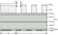
首先,执行步骤S201、在具有阵列区域和外围区域的基底上形成叠层结构。Firstly, step S201 is performed to form a laminated structure on a substrate having an array area and a peripheral area.
如图3a所示,在基底200上形成叠层结构201,其中,叠层结构201包括由下至上依次堆叠的第一牺牲层201a、第一支撑层201b、第二牺牲层201c和第二支撑层201d。基底200包括阵列区域A和外围区域B,且基底200中形成有接触结构200a和覆盖接触结构200a的绝缘层200b。As shown in FIG. 3a, a
接下来,执行步骤S202、在叠层结构上形成第一掩膜层;其中,对应于阵列区域的第一掩膜层具有第一图案。Next, step S202 is performed to form a first mask layer on the stacked structure; wherein, the first mask layer corresponding to the array region has a first pattern.
在一些实施例中,步骤S202可以通过以下步骤形成:In some embodiments, step S202 may be formed by the following steps:
步骤S2021、在叠层结构上依次形成第一初始掩膜层和第二初始掩膜层;其中,第二初始掩膜层中形成有第一图案。Step S2021 , sequentially forming a first initial mask layer and a second initial mask layer on the laminated structure; wherein, the first pattern is formed in the second initial mask layer.
如图3b所示,在叠层结构201的表面依次形成第一初始掩膜层202a第二初始掩膜层203a,其中,对应于阵列区域A上的第二初始掩膜层203a中形成有第一图案。As shown in FIG. 3b, a first
本申请实施例中,对应于外围区域B上的第二初始掩膜层203a中形成有第二图案,且第二图案的图案密度小于第一图案的图案密度。In the embodiment of the present application, a second pattern is formed in the second
本申请实施例中,可以通过任意一种合适的沉积工艺形成第一初始掩膜层和第二初始掩膜层,例如,化学气相沉积(Chemical Vapor Deposition,CVD)工艺、物理气相沉积(Physical Vapor Deposition,PVD)工艺、原子层沉积(Atomic Layer Deposition,ALD)工艺、旋涂工艺或者涂敷工艺。In the embodiment of the present application, the first initial mask layer and the second initial mask layer can be formed by any suitable deposition process, for example, chemical vapor deposition (Chemical Vapor Deposition, CVD) process, physical vapor deposition (Physical Vapor Deposition) Deposition, PVD) process, atomic layer deposition (Atomic Layer Deposition, ALD) process, spin coating process or coating process.
步骤S2022、通过第二初始掩膜层刻蚀第一初始掩膜层,以实现将第一图案转移至第一初始掩膜层中,形成第一掩膜层。Step S2022 , etching the first initial mask layer through the second initial mask layer, so as to transfer the first pattern to the first initial mask layer, and form a first mask layer.
请继续参见图3b,通过第二初始掩膜层203a刻蚀第一初始掩膜层202a,以将第二初始掩膜层203a中的第一图案转移至第一初始掩膜层202a中,得到如图3c所示的第一掩膜层202。其中,第一掩膜层202暴露出部分叠层结构201的表面。Please continue to refer to FIG. 3b, the first
值得注意的是,在通过第二初始掩膜层203a刻蚀第一初始掩膜层202a的过程中,由于阵列区域A与外围区域B上图案的图案密度不同所带来的刻蚀负载效应,导致阵列区域A上的第二初始掩膜层的厚度h1,小于外围区域B上的第二初始掩膜层的厚度h2。It should be noted that during the process of etching the first
在一些实施例中,半导体结构的制备方法还包括:在形成第一掩膜层之后,去除第二初始掩膜层。In some embodiments, the manufacturing method of the semiconductor structure further includes: after forming the first mask layer, removing the second initial mask layer.
如图3d所示,可以通过干法或者湿法刻蚀工艺去除第二初始掩膜层203a。As shown in FIG. 3d, the second
接下来,执行步骤S203,对阵列区域上的第一掩膜层进行离子掺杂,得到掺杂后的第一掩膜层。Next, step S203 is performed to perform ion doping on the first mask layer on the array region to obtain a doped first mask layer.
在一些实施例中,步骤S203可以包括以下步骤:In some embodiments, step S203 may include the following steps:
步骤S2031、在第一掩膜层和部分叠层结构上沉积牺牲层。Step S2031 , depositing a sacrificial layer on the first mask layer and part of the stacked structure.
本申请实施例中,牺牲层可以是旋涂硬掩膜层(Spin-On Hard Mask,SOH)、旋涂碳层或者其它硬掩膜层。In the embodiment of the present application, the sacrificial layer may be a spin-on hard mask layer (Spin-On Hard Mask, SOH), a spin-on carbon layer or other hard mask layers.
请继续参见图3d,在第一掩膜层202和部分叠层结构201上形成如图3e所示的牺牲层204。本申请实施例中,可以通过任意一种合适的沉积工艺形成牺牲层204。Please continue to refer to FIG. 3 d , a
步骤S2032、刻蚀阵列区域上的牺牲层,以暴露出阵列区域上的部分第一掩膜层。Step S2032, etching the sacrificial layer on the array area to expose part of the first mask layer on the array area.
在一些实施例中,步骤S2032可以通过以下步骤形成:In some embodiments, step S2032 may be formed by the following steps:
步骤S10、在牺牲层上形成第二掩膜层。Step S10, forming a second mask layer on the sacrificial layer.
本申请实施例中,第二掩膜层包括抗反射涂层(Anti-Reflective Coating,ARC)和光刻胶层(Photoresist,PR),且抗反射涂层包括介电抗反射涂层(Dielectric Anti-Reflective Coating,DARC)和底部抗反射涂层(Bottom Anti-Reflective Coating,BARC)。In the embodiment of the present application, the second mask layer includes an antireflective coating (Anti-Reflective Coating, ARC) and a photoresist layer (Photoresist, PR), and the antireflective coating includes a dielectric antireflective coating (Dielectric Antireflective Coating). -Reflective Coating, DARC) and bottom anti-reflective coating (Bottom Anti-Reflective Coating, BARC).
请继续参见图3e,在牺牲层204上形成如图3f所示的第二掩膜层205,第二掩膜层205包括由下至上依次堆叠的介电抗反射涂层205a、底部抗反射涂层205b和光刻胶层205c。本申请实施例中,可以通过任意一种合适的沉积工艺形成介电抗反射涂层205a、底部抗反射涂层205b和光刻胶层205c。Please continue to refer to FIG. 3e, on the
步骤S11、图形化第二掩膜层,暴露出对应于阵列区域的牺牲层。Step S11 , patterning the second mask layer to expose the sacrificial layer corresponding to the array area.
请继续参见图3f和3g,采用预设的掩膜版C,对光刻胶层205c、底部抗反射涂层205b和介电抗反射涂层205a进行曝光处理,得到如图3g所示的图形化的光刻胶层206c、图形化的底部抗反射涂层206b和图形化的介电抗反射涂层206a,暴露出对应于阵列区域A的牺牲层204。Please continue to refer to Figures 3f and 3g, using the preset mask C to expose the
步骤S12、刻蚀去除部分暴露的牺牲层,以暴露出部分第一掩膜层。Step S12 , etching and removing part of the exposed sacrificial layer, so as to expose part of the first mask layer.
如图3h所示,刻蚀去除部分暴露出来的牺牲层,保留位于外围区域B上的部分牺牲层204a,暴露出了第一掩膜层202。这里,可以通过干法刻蚀工艺或者湿法刻蚀工艺刻蚀去除部分暴露的牺牲层。As shown in FIG. 3 h , part of the exposed sacrificial layer is removed by etching, and part of the
步骤S2033、对暴露出的第一掩膜层进行离子掺杂,得到掺杂后的第一掩膜层。Step S2033 , performing ion doping on the exposed first mask layer to obtain a doped first mask layer.
本申请实施例中,对暴露出的第一掩膜层进行离子掺杂的过程可以是:采用特定的离子发生器,产生高速离子,通过高速离子轰击暴露出的第一掩膜层的表面,从而实现对暴露出的第一掩膜层进行掺杂。这里,对暴露出的第一掩膜层进行掺杂的离子类型可以是P型离子,例如,硼离子。即本申请实施例中,在离子掺杂之前,不论第一掩膜层是未掺杂、N型离子掺杂或者是P型离子掺杂,均对暴露出的第一掩膜层进行P型离子掺杂,以使得P型离子掺杂后的第一掩膜层相较于离子掺杂之前的第一掩膜层的刻蚀速率更慢。In the embodiment of the present application, the process of ion doping the exposed first mask layer may be: using a specific ion generator to generate high-speed ions, bombarding the surface of the exposed first mask layer by high-speed ions, In this way, the exposed first mask layer is doped. Here, the ion type for doping the exposed first mask layer may be P-type ions, for example, boron ions. That is, in the embodiment of the present application, before ion doping, regardless of whether the first mask layer is undoped, N-type ion-doped or P-type ion-doped, the exposed first mask layer is P-type Ion doping, so that the etching rate of the first mask layer after P-type ion doping is slower than that of the first mask layer before ion doping.
在一些实施例中,第一掩膜层的厚度在500纳米(nm)至800nm之间,对暴露出的第一掩膜层进行离子掺杂的能量在10千电子伏(Kev)至100Kev之间,对暴露出的第一掩膜层进行离子掺杂的剂量在1013原子/cm2至1015原子/cm2之间。In some embodiments, the thickness of the first mask layer is between 500 nanometers (nm) and 800 nm, and the ion doping energy for the exposed first mask layer is between 10 kiloelectron volts (Kev) and 100 Kev. During the period, the ion doping dose for the exposed first mask layer is between 1013 atoms/cm2 and 1015 atoms/cm2 .
需要说明的是,本申请实施例中,对暴露出的第一掩膜层进行掺杂的程度是:使得掺杂后的第一掩膜层相对于叠层结构的刻蚀选择比,大于未掺杂的第一掩膜层相对于叠层结构的刻蚀选择比。It should be noted that, in the embodiment of the present application, the degree of doping the exposed first mask layer is such that the etching selectivity ratio of the doped first mask layer relative to the stacked structure is greater than that of the undoped first mask layer. The etching selectivity ratio of the doped first mask layer relative to the stacked structure.
请继续参见图3h,对阵列区域A上暴露出的第一掩膜层进行离子掺杂,得到如图3i所示的位于阵列区域A上的掺杂后的第一掩膜层202b。由于外围区域B上的第一掩膜层表面覆盖有部分牺牲层204a、图形化的光刻胶层206c、图形化的底部抗反射涂层206b和图形化的介电抗反射涂层206a,因此,对外围区域B上的第一掩膜层202未进行离子掺杂。Please continue to refer to FIG. 3h , the first mask layer exposed on the array region A is ion-doped to obtain the doped
本申请实施例中,掺杂后的第一掩膜层202b与叠层结构201之间的刻蚀选择比,大于未进行离子掺杂的第一掩膜层202与叠层结构201之间的刻蚀选择比。In the embodiment of the present application, the etching selectivity ratio between the doped
在一些实施例中,在对暴露出的第一掩膜层进行离子掺杂之后,半导体结构的制备方法还包括:去除外围区域上的第二掩膜层和剩余的牺牲层,暴露出外围区域上的第一掩膜层。In some embodiments, after performing ion doping on the exposed first mask layer, the manufacturing method of the semiconductor structure further includes: removing the second mask layer and the remaining sacrificial layer on the peripheral region, exposing the peripheral region on the first mask layer.
如图3j所示,在得到掺杂后的第一掩膜层202b之后,可以采用湿法或者干法刻蚀技术刻蚀去除外围区域B上的第二掩膜层(即图形化的光刻胶层206c、图形化的底部抗反射涂层206b和图形化的介电抗反射涂层206a)和剩余的牺牲层,暴露出外围区域B上的第一掩膜层202。As shown in FIG. 3j, after obtaining the doped
本申请实施例中,对阵列区域上的第一掩膜层进行离子掺杂的目的是,提高阵列区域上第一掩膜层的刻蚀难度,使得掺杂后的第一掩膜层与叠层结构之间的刻蚀选择比,大于未进行离子掺杂的第一掩膜层与叠层结构之间的刻蚀选择比。In the embodiment of the present application, the purpose of ion doping the first mask layer on the array region is to improve the etching difficulty of the first mask layer on the array region, so that the doped first mask layer and the stack The etching selectivity ratio between the layer structures is greater than the etching selectivity ratio between the first mask layer without ion doping and the laminated structure.
接下来,执行步骤S204、通过掺杂后的第一掩膜层刻蚀叠层结构,以将第一图案转移至叠层结构中。Next, step S204 is performed to etch the stacked structure through the doped first mask layer, so as to transfer the first pattern into the stacked structure.
在一些实施例中,第一图案可以是电容孔图案,步骤S204可以包括以下步骤:In some embodiments, the first pattern may be a capacitor hole pattern, and step S204 may include the following steps:
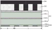
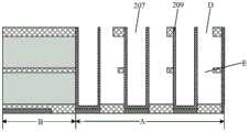
通过掺杂后的第一掩膜层,依次刻蚀第二支撑层、第二牺牲层、第一支撑层和第一牺牲层,以将电容孔图案转移至叠层结构中,在叠层结构中形成多个电容孔和位于相邻两个电容孔之间的刻蚀柱;其中,电容孔暴露出部分接触结构。Through the doped first mask layer, etch the second supporting layer, the second sacrificial layer, the first supporting layer and the first sacrificial layer in sequence, so as to transfer the capacitor hole pattern to the stacked structure, in the stacked structure A plurality of capacitor holes and an etching column between two adjacent capacitor holes are formed; wherein, the capacitor holes expose part of the contact structure.
请继续参见图3j,通过掺杂后的第一掩膜层202b,依次刻蚀第二支撑层201d、第二牺牲层201c、第一支撑层201b、第一牺牲层201a和部分绝缘层200b,形成如图3k所示的多个电容孔207和位于相邻两个电容孔之间的刻蚀柱(即定义电容孔的图形)208。其中,每一电容孔207暴露出接触结构200a。Please continue to refer to FIG. 3j, through the doped
在一些实施例中,在形成电容孔之后,半导体结构的制备方法还包括:去除第一掩膜层。In some embodiments, after forming the capacitor hole, the method for manufacturing the semiconductor structure further includes: removing the first mask layer.
如图3l所示,在形成电容孔207之后,通过干法刻蚀工艺去除了第一掩膜层(包括位于阵列区域A上掺杂后的第一掩膜层202b和位于外围区域B上未掺杂的第一掩膜层202),暴露出了刻蚀柱208的顶表面。As shown in FIG. 3l, after the
本申请实施例中,由于位于阵列区域上的掺杂后的第一掩膜层与叠层结构之间的刻蚀选择比,大于位于外围区域上未进行离子掺杂的第一掩膜层与叠层结构之间的刻蚀选择比,如此,可以抵消不同区域上的第一掩膜层在刻蚀过程中所带来的刻蚀负载效应,这样在后续刻蚀去除第一掩膜层时,不会损伤刻蚀柱,进而也就不会影响所形成的电容结构的容量。In the embodiment of the present application, since the etching selectivity ratio between the doped first mask layer on the array region and the stacked structure is greater than that of the first mask layer not ion-doped on the peripheral region and The etch selectivity ratio between stacked structures, in this way, can offset the etch load effect brought by the first mask layer on different regions during the etching process, so that when the first mask layer is removed by subsequent etching , will not damage the etched pillars, and thus will not affect the capacity of the formed capacitor structure.
在一些实施例中,在去除第一掩膜层之后,半导体结构的制备方法还包括:处理刻蚀柱,形成电容结构。In some embodiments, after removing the first mask layer, the method for manufacturing the semiconductor structure further includes: processing the etched pillars to form a capacitor structure.
在一些实施例中,处理刻蚀柱,形成电容结构,包括:In some embodiments, processing the etched pillar to form the capacitor structure includes:
步骤S20、在电容孔的内壁和刻蚀柱的表面形成第一电极层。Step S20, forming a first electrode layer on the inner wall of the capacitor hole and the surface of the etched pillar.
第一电极层可以是氮化钛层。The first electrode layer may be a titanium nitride layer.
步骤S21、在第二支撑层中形成第一开口。Step S21 , forming a first opening in the second supporting layer.
步骤S22、通过第一开口去除第二牺牲层。Step S22 , removing the second sacrificial layer through the first opening.
步骤S23、在第一支撑层中形成第二开口。Step S23 , forming a second opening in the first supporting layer.
步骤S24、通过第二开口去除第一牺牲层。Step S24 , removing the first sacrificial layer through the second opening.
如图3m所示,在电容孔207的内壁和刻蚀柱的表面形成第一电极层209;在第二支撑层中形成第一开口D,通过第一开口D去除了第二牺牲层;在第一支撑层中形成第二开口E,通过第一开口E去除了第一牺牲层。As shown in FIG. 3m, a
本申请实施例中,可以采用干法刻蚀技术,例如,等离子刻蚀技术形成第一开口D和第二开口E。In the embodiment of the present application, the first opening D and the second opening E may be formed by using a dry etching technique, for example, a plasma etching technique.
本申请实施例中,可以采用湿法刻蚀技术,例如,采用硫酸、氢氟酸、硝酸等腐蚀液去除第二牺牲层和第一牺牲层。In the embodiment of the present application, a wet etching technique may be used, for example, sulfuric acid, hydrofluoric acid, nitric acid and other etching solutions are used to remove the second sacrificial layer and the first sacrificial layer.
步骤S25、在第一电极层的表面依次沉积电介质层和第二电极层,形成电容结构。Step S25 , depositing a dielectric layer and a second electrode layer sequentially on the surface of the first electrode layer to form a capacitor structure.
如图3n所示,在第一电极层209的表面形成电介质层210和第二电极层211。本申请实施例中,电介质层210可以是氧化锆层和/或氧化铝层,也可以是其它高介电常数材料层;第二电极层211与第一电极层209可以相同,也可以不同。As shown in FIG. 3 n , a
在一些实施例中,半导体结构的形成方法还包括:在第二电极层之间沉积导电材料。导电材料可以是多晶硅,也可以是其它任意一种合适的导电材料,例如,钨、钴或者掺杂多晶硅。In some embodiments, the method for forming the semiconductor structure further includes: depositing a conductive material between the second electrode layers. The conductive material may be polysilicon, or any other suitable conductive material, such as tungsten, cobalt or doped polysilicon.
本申请实施例提供的半导体结构的制备方法,通过对阵列区域上的第一掩膜层进行掺杂,使得阵列区域上的第一掩膜层和外围区域上的第一掩膜层具有不同的刻蚀选择比,如此,可以抵消不同区域上的第一掩膜层在刻蚀过程中所带来的刻蚀负载效应,进而可以提高电容图案的完整性和所形成的电容结构的容量。In the manufacturing method of the semiconductor structure provided by the embodiment of the present application, by doping the first mask layer on the array region, the first mask layer on the array region and the first mask layer on the peripheral region have different The etching selectivity, in this way, can offset the etching load effect brought by the first mask layer on different regions during the etching process, thereby improving the integrity of the capacitor pattern and the capacity of the formed capacitor structure.
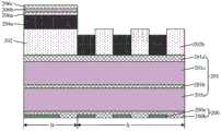
除此之外,本申请实施例还提供一种半导体结构,半导体结构通过上述实施例提供的半导体结构的制备方法制备。图4为本申请一个实施例提供的半导体结构的一种剖面图,如图4所示,半导体结构40包括:基底200和电容结构;其中,基底200包括接触结构200a和覆盖接触结构200a的绝缘层,接触结构200a用于与形成的电容结构电连接。In addition, the embodiment of the present application also provides a semiconductor structure, which is prepared by the method for preparing the semiconductor structure provided in the above embodiment. FIG. 4 is a cross-sectional view of a semiconductor structure provided by an embodiment of the present application. As shown in FIG. 4, the semiconductor structure 40 includes: a
本申请实施例中,基底200包括阵列区域A和外围区域B,电容结构位于基底200的阵列区域A的表面。In the embodiment of the present application, the
请继续参见图4,电容结构包括依次堆叠的第一电极层209、电介质层210和第二电极层211,且相邻的第二电极层211之间填充有导电材料212。Please continue to refer to FIG. 4 , the capacitor structure includes a
本申请实施例中,电容结构为杯状结构,电容结构还包括平行设置的第一支撑层213和第二支撑层214;其中,第一支撑层213设置于电容结构的中部外周,第二支撑层214设置于电容结构的顶部外周,第一支撑层213和第二支撑层214共同用于支撑电容结构。In the embodiment of the present application, the capacitor structure is a cup-shaped structure, and the capacitor structure also includes a first supporting
在一些实施例中,第二支撑层214的厚度h3大于第一支撑层213的厚度h4,如此,可以实现更好的支撑效果。In some embodiments, the thickness h3 of the second supporting
本申请实施例中的半导体结构与上述实施例中的半导体结构的制备方法类似,对于本申请实施例未详尽披露的技术特征,请参考上述实施例进行理解,这里,不再赘述。The semiconductor structure in the embodiment of the present application is similar to the method for preparing the semiconductor structure in the above-mentioned embodiment. For the technical features not disclosed in detail in the embodiment of the present application, please refer to the above-mentioned embodiment for understanding, and details will not be repeated here.
本申请实施例提供的半导体结构,由于具有完整的电容图案,如此,可以提高所形成的电容结构的容量。Since the semiconductor structure provided by the embodiment of the present application has a complete capacitor pattern, the capacity of the formed capacitor structure can be improved.
在本申请所提供的几个实施例中,应该理解到,所揭露的设备和方法,可以通过非目标的方式实现。以上所描述的设备实施例仅仅是示意性的,例如,单元的划分,仅仅为一种逻辑功能划分,实际实现时可以有另外的划分方式,如:多个单元或组件可以结合,或可以集成到另一个系统,或一些特征可以忽略,或不执行。另外,所显示或讨论的各组成部分相互之间的耦合、或直接耦合。In the several embodiments provided in this application, it should be understood that the disclosed devices and methods may be implemented in non-target ways. The device embodiments described above are only illustrative. For example, the division of units is only a logical function division. In actual implementation, there may be other division methods, such as: multiple units or components can be combined or integrated. to another system, or some features may be ignored, or not implemented. In addition, the various components shown or discussed are coupled with each other, or directly coupled.
上述作为分离部件说明的单元可以是、或也可以不是物理上分开的,作为单元显示的部件可以是、或也可以不是物理单元,即可以位于一个地方,也可以分布到多个网络单元上;可以根据实际的需要选择其中的部分或全部单元来实现本实施例方案的目的。The units described above as separate components may or may not be physically separated, and the components displayed as units may or may not be physical units, that is, they may be located in one place or distributed to multiple network units; Part or all of the units can be selected according to actual needs to achieve the purpose of the solution of this embodiment.
本申请所提供的几个方法或设备实施例中所揭露的特征,在不冲突的情况下可以任意组合,得到新的方法实施例或设备实施例。The features disclosed in several method or device embodiments provided in this application can be combined arbitrarily without conflict to obtain new method embodiments or device embodiments.
以上所述,仅为本申请实施例的一些实施方式,但本申请实施例的保护范围并不局限于此,任何熟悉本技术领域的技术人员在本申请实施例揭露的技术范围内,可轻易想到变化或替换,都应涵盖在本申请实施例的保护范围之内。因此,本申请实施例的保护范围应以权利要求的保护范围为准。The above are only some implementations of the embodiments of the present application, but the scope of protection of the embodiments of the present application is not limited thereto. Anyone familiar with the technical field can easily Any changes or substitutions that come to mind should be covered within the protection scope of the embodiments of the present application. Therefore, the protection scope of the embodiments of the present application should be determined by the protection scope of the claims.
Claims (15)
Translated fromChinesePriority Applications (3)
| Application Number | Priority Date | Filing Date | Title |
|---|---|---|---|
| CN202111298101.8ACN116096071B (en) | 2021-11-04 | 2021-11-04 | Semiconductor structure and preparation method thereof |
| PCT/CN2021/135767WO2023077602A1 (en) | 2021-11-04 | 2021-12-06 | Semiconductor structure and preparation method therefor |
| US17/804,178US12432940B2 (en) | 2021-11-04 | 2022-05-26 | Semiconductor structure and method for manufacturing same |
Applications Claiming Priority (1)
| Application Number | Priority Date | Filing Date | Title |
|---|---|---|---|
| CN202111298101.8ACN116096071B (en) | 2021-11-04 | 2021-11-04 | Semiconductor structure and preparation method thereof |
Publications (2)
| Publication Number | Publication Date |
|---|---|
| CN116096071Atrue CN116096071A (en) | 2023-05-09 |
| CN116096071B CN116096071B (en) | 2025-08-22 |
Family
ID=86203030
Family Applications (1)
| Application Number | Title | Priority Date | Filing Date |
|---|---|---|---|
| CN202111298101.8AActiveCN116096071B (en) | 2021-11-04 | 2021-11-04 | Semiconductor structure and preparation method thereof |
Country Status (2)
| Country | Link |
|---|---|
| CN (1) | CN116096071B (en) |
| WO (1) | WO2023077602A1 (en) |
Families Citing this family (1)
| Publication number | Priority date | Publication date | Assignee | Title |
|---|---|---|---|---|
| WO2024234349A1 (en)* | 2023-05-17 | 2024-11-21 | 长江存储科技有限责任公司 | Semiconductor structure and manufacturing method therefor, memory, and memory system |
Citations (6)
| Publication number | Priority date | Publication date | Assignee | Title |
|---|---|---|---|---|
| JP2001237173A (en)* | 2000-02-24 | 2001-08-31 | Sony Corp | Resist pattern forming method and semiconductor device manufacturing method |
| KR20030085784A (en)* | 2002-05-02 | 2003-11-07 | 동부전자 주식회사 | Dram fabrication capable of high integration and fabrication method |
| US20050070064A1 (en)* | 2003-09-25 | 2005-03-31 | International Business Machines Corporation | Self-limited metal recess for deep trench metal fill |
| US20050212026A1 (en)* | 2004-03-26 | 2005-09-29 | Suk-Jin Chung | Trench capacitors with insulating layer collars in undercut regions and method of fabricating the same |
| US20170178914A1 (en)* | 2015-12-21 | 2017-06-22 | Varian Semiconductor Equipment Associates, Inc. | Etch Rate Modulation Through Ion Implantation |
| KR20170103204A (en)* | 2016-03-03 | 2017-09-13 | 에스케이하이닉스 주식회사 | Method for manufacturing semiconductor device |
Family Cites Families (4)
| Publication number | Priority date | Publication date | Assignee | Title |
|---|---|---|---|---|
| KR20060010927A (en)* | 2004-07-29 | 2006-02-03 | 주식회사 하이닉스반도체 | Semiconductor device manufacturing method |
| JP2007335660A (en)* | 2006-06-15 | 2007-12-27 | Toshiba Corp | Pattern forming method for semiconductor device |
| CN103663357B (en)* | 2012-09-18 | 2017-07-07 | 无锡华润上华半导体有限公司 | The lithographic method of silicon |
| CN110265290B (en)* | 2019-06-27 | 2020-06-30 | 英特尔半导体(大连)有限公司 | Method for enhancing semiconductor etching capability |
- 2021
- 2021-11-04CNCN202111298101.8Apatent/CN116096071B/enactiveActive
- 2021-12-06WOPCT/CN2021/135767patent/WO2023077602A1/ennot_activeCeased
Patent Citations (6)
| Publication number | Priority date | Publication date | Assignee | Title |
|---|---|---|---|---|
| JP2001237173A (en)* | 2000-02-24 | 2001-08-31 | Sony Corp | Resist pattern forming method and semiconductor device manufacturing method |
| KR20030085784A (en)* | 2002-05-02 | 2003-11-07 | 동부전자 주식회사 | Dram fabrication capable of high integration and fabrication method |
| US20050070064A1 (en)* | 2003-09-25 | 2005-03-31 | International Business Machines Corporation | Self-limited metal recess for deep trench metal fill |
| US20050212026A1 (en)* | 2004-03-26 | 2005-09-29 | Suk-Jin Chung | Trench capacitors with insulating layer collars in undercut regions and method of fabricating the same |
| US20170178914A1 (en)* | 2015-12-21 | 2017-06-22 | Varian Semiconductor Equipment Associates, Inc. | Etch Rate Modulation Through Ion Implantation |
| KR20170103204A (en)* | 2016-03-03 | 2017-09-13 | 에스케이하이닉스 주식회사 | Method for manufacturing semiconductor device |
Also Published As
| Publication number | Publication date |
|---|---|
| CN116096071B (en) | 2025-08-22 |
| WO2023077602A1 (en) | 2023-05-11 |
Similar Documents
| Publication | Publication Date | Title |
|---|---|---|
| US4650544A (en) | Shallow groove capacitor fabrication method | |
| US5930640A (en) | Mechanical supports for very thin stacked capacitor plates | |
| TW201007889A (en) | Methods of forming a plurality of capacitors | |
| CN111710682A (en) | Three-dimensional memory and preparation method thereof | |
| JPH09232540A (en) | Manufacture of semiconductor device | |
| US20220093509A1 (en) | Contact window structure, metal plug and forming method thereof, and semiconductor structure | |
| US12402295B2 (en) | Method for fabricating semiconductor device and semiconductor device | |
| CN210110740U (en) | Capacitor array and storage device | |
| WO2023077602A1 (en) | Semiconductor structure and preparation method therefor | |
| JP2006319058A (en) | Manufacturing method of semiconductor device | |
| CN115996561B (en) | Method for forming capacitor and semiconductor device | |
| CN115241372B (en) | Memory device, semiconductor structure and method for forming the same | |
| KR100465865B1 (en) | Method for forming storage node electrode in MML device | |
| CN116264766B (en) | Semiconductor structure forming method, stacked structure and forming method thereof | |
| US12432940B2 (en) | Semiconductor structure and method for manufacturing same | |
| US11374011B1 (en) | Method of manufacturing dynamic random access memory | |
| CN116156875A (en) | Semiconductor structure and forming method thereof | |
| US7208095B2 (en) | Method for fabricating bottom electrodes of stacked capacitor memory cells and method for cleaning and drying a semiconductor wafer | |
| EP3840034B1 (en) | Method for producing nanoscaled electrically conductive lines for semiconductor devices | |
| CN119486103B (en) | Semiconductor structure and preparation method thereof | |
| CN118338649A (en) | Semiconductor structure and forming method thereof | |
| CN118338650A (en) | Method for forming semiconductor structure and storage structure | |
| KR20010093011A (en) | Method of fabricating a semiconductor device | |
| CN118338652A (en) | Semiconductor structure and forming method thereof | |
| CN118338651A (en) | Semiconductor structure and forming method thereof |
Legal Events
| Date | Code | Title | Description |
|---|---|---|---|
| PB01 | Publication | ||
| PB01 | Publication | ||
| SE01 | Entry into force of request for substantive examination | ||
| SE01 | Entry into force of request for substantive examination | ||
| GR01 | Patent grant | ||
| GR01 | Patent grant |