CN116094307A - Power factor correction converter, controller and digital peak hold circuit thereof - Google Patents
Power factor correction converter, controller and digital peak hold circuit thereofDownload PDFInfo
- Publication number
- CN116094307A CN116094307ACN202210695955.8ACN202210695955ACN116094307ACN 116094307 ACN116094307 ACN 116094307ACN 202210695955 ACN202210695955 ACN 202210695955ACN 116094307 ACN116094307 ACN 116094307A
- Authority
- CN
- China
- Prior art keywords
- signal
- digital
- input signal
- peak
- generate
- Prior art date
- Legal status (The legal status is an assumption and is not a legal conclusion. Google has not performed a legal analysis and makes no representation as to the accuracy of the status listed.)
- Pending
Links
Images


Classifications
- H—ELECTRICITY
- H02—GENERATION; CONVERSION OR DISTRIBUTION OF ELECTRIC POWER
- H02M—APPARATUS FOR CONVERSION BETWEEN AC AND AC, BETWEEN AC AND DC, OR BETWEEN DC AND DC, AND FOR USE WITH MAINS OR SIMILAR POWER SUPPLY SYSTEMS; CONVERSION OF DC OR AC INPUT POWER INTO SURGE OUTPUT POWER; CONTROL OR REGULATION THEREOF
- H02M1/00—Details of apparatus for conversion
- H02M1/42—Circuits or arrangements for compensating for or adjusting power factor in converters or inverters
- H02M1/4208—Arrangements for improving power factor of AC input
- H02M1/4225—Arrangements for improving power factor of AC input using a non-isolated boost converter
- H—ELECTRICITY
- H02—GENERATION; CONVERSION OR DISTRIBUTION OF ELECTRIC POWER
- H02M—APPARATUS FOR CONVERSION BETWEEN AC AND AC, BETWEEN AC AND DC, OR BETWEEN DC AND DC, AND FOR USE WITH MAINS OR SIMILAR POWER SUPPLY SYSTEMS; CONVERSION OF DC OR AC INPUT POWER INTO SURGE OUTPUT POWER; CONTROL OR REGULATION THEREOF
- H02M1/00—Details of apparatus for conversion
- H02M1/32—Means for protecting converters other than automatic disconnection
- H02M1/322—Means for rapidly discharging a capacitor of the converter for protecting electrical components or for preventing electrical shock
- H—ELECTRICITY
- H02—GENERATION; CONVERSION OR DISTRIBUTION OF ELECTRIC POWER
- H02M—APPARATUS FOR CONVERSION BETWEEN AC AND AC, BETWEEN AC AND DC, OR BETWEEN DC AND DC, AND FOR USE WITH MAINS OR SIMILAR POWER SUPPLY SYSTEMS; CONVERSION OF DC OR AC INPUT POWER INTO SURGE OUTPUT POWER; CONTROL OR REGULATION THEREOF
- H02M3/00—Conversion of DC power input into DC power output
- H02M3/02—Conversion of DC power input into DC power output without intermediate conversion into AC
- H02M3/04—Conversion of DC power input into DC power output without intermediate conversion into AC by static converters
- H02M3/10—Conversion of DC power input into DC power output without intermediate conversion into AC by static converters using discharge tubes with control electrode or semiconductor devices with control electrode
- H02M3/145—Conversion of DC power input into DC power output without intermediate conversion into AC by static converters using discharge tubes with control electrode or semiconductor devices with control electrode using devices of a triode or transistor type requiring continuous application of a control signal
- H02M3/155—Conversion of DC power input into DC power output without intermediate conversion into AC by static converters using discharge tubes with control electrode or semiconductor devices with control electrode using devices of a triode or transistor type requiring continuous application of a control signal using semiconductor devices only
- H02M3/156—Conversion of DC power input into DC power output without intermediate conversion into AC by static converters using discharge tubes with control electrode or semiconductor devices with control electrode using devices of a triode or transistor type requiring continuous application of a control signal using semiconductor devices only with automatic control of output voltage or current, e.g. switching regulators
- H02M3/157—Conversion of DC power input into DC power output without intermediate conversion into AC by static converters using discharge tubes with control electrode or semiconductor devices with control electrode using devices of a triode or transistor type requiring continuous application of a control signal using semiconductor devices only with automatic control of output voltage or current, e.g. switching regulators with digital control
- Y—GENERAL TAGGING OF NEW TECHNOLOGICAL DEVELOPMENTS; GENERAL TAGGING OF CROSS-SECTIONAL TECHNOLOGIES SPANNING OVER SEVERAL SECTIONS OF THE IPC; TECHNICAL SUBJECTS COVERED BY FORMER USPC CROSS-REFERENCE ART COLLECTIONS [XRACs] AND DIGESTS
- Y02—TECHNOLOGIES OR APPLICATIONS FOR MITIGATION OR ADAPTATION AGAINST CLIMATE CHANGE
- Y02B—CLIMATE CHANGE MITIGATION TECHNOLOGIES RELATED TO BUILDINGS, e.g. HOUSING, HOUSE APPLIANCES OR RELATED END-USER APPLICATIONS
- Y02B70/00—Technologies for an efficient end-user side electric power management and consumption
- Y02B70/10—Technologies improving the efficiency by using switched-mode power supplies [SMPS], i.e. efficient power electronics conversion e.g. power factor correction or reduction of losses in power supplies or efficient standby modes
Landscapes
- Engineering & Computer Science (AREA)
- Power Engineering (AREA)
- Rectifiers (AREA)
- Measurement Of Current Or Voltage (AREA)
- Dc-Dc Converters (AREA)
Abstract
Translated fromChinese
Description
Translated fromChinese技术领域technical field
本发明涉及一种转换器,特别涉及一种功率因数校正转换器。本发明还涉及一种适于功率因数校正转换器的功率因数校正控制器及数字峰值保持电路。The invention relates to a converter, in particular to a power factor correction converter. The invention also relates to a power factor correction controller and a digital peak holding circuit suitable for a power factor correction converter.
背景技术Background technique
功率因数校正转换器(Power Factor Correction converter,PFC converter)是电源领域中常见的一种电路,其经常被应用于电源供应器(Power supply)中以解决功率损耗(power loss)的问题,其中功率损耗的问题与功率因数(Power Factor,PF)有相关。功率因数的定义为实际功率与视在功率之间的比值,其中实际功率为一供应电源(例如为电源供应器)所耦接的一负载所实际消耗的功率,视在功率为所述供应电源需要提供的总功率。一般来说,功率因数介于0至1之间,其中当功率因数的值小于1时,代表所述供应电源所提供的电压与电流之间不同相(phase),进而导致所述功率损耗的问题;而当功率因数的值愈接近于0时,代表所述功率损耗的问题愈严重。The power factor correction converter (Power Factor Correction converter, PFC converter) is a common circuit in the field of power supply, which is often used in the power supply (Power supply) to solve the problem of power loss (power loss), where the power The problem of loss is related to power factor (Power Factor, PF). Power factor is defined as the ratio between real power and apparent power, where real power is the power actually consumed by a load coupled to a power supply (such as a power supply), and apparent power is the power of the power supply The total power that needs to be provided. Generally speaking, the power factor is between 0 and 1, wherein when the value of the power factor is less than 1, it means that the voltage and current provided by the power supply are out of phase, which leads to the loss of power. problem; and when the value of the power factor is closer to 0, it means that the problem of power loss is more serious.
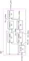
请参照图1A,图1A是现有技术的功率因数校正转换器10的模块方块图。如图1A所示,现有技术的功率因数校正转换器10包含一整流器101、一功率因数校正控制器102以及一功率级电路103,其中功率因数校正转换器10用以将一交流电压Vac转换为与其同相的一输出电压Vo,使其功率因数的值接近于1,进而避免功率损耗的问题。Please refer to FIG. 1A , which is a block diagram of a power
尽管现有技术的功率因数校正转换器10可以改善功率损耗的问题,其依旧有着电路尺寸、成本及运作时整体功耗较大的问题存在。请参照图1B,图1B是现有技术的功率因数校正转换器10中整流电压Vi与输出电压Vo之间的波形比较图。如图1B所示,波形W1为输出电压Vo的波形,波形W2为整流电压Vi的波形,其中输出电压Vo的值为一固定的值(例如为400伏特),整流电压Vi通过整流器101将交流电压Vac整流后而产生。如图1B的虚线方框Sq1所示,当整流电压Vi的峰值(peak)较低时(例如为85伏特),现有技术的功率因数校正转换器10依旧会将其转换为具有较大固定值(400伏特)的输出电压Vo。由于整流电压Vi的峰值与输出电压Vo之间的压差较大(例如为315伏特),使得现有技术的功率因数校正转换器10中必须采用尺寸较大的储能元件(例如,电容器或电感器)及开关(例如,二极管或晶体管)以避免电路烧坏,进而使现有技术的功率因数校正转换器10的成本及运作时的整体功耗较大。Although the power factor correction converter 10 in the prior art can improve the problem of power loss, it still has the problems of circuit size, cost and overall power consumption during operation. Please refer to FIG. 1B . FIG. 1B is a waveform comparison diagram between the rectified voltage Vi and the output voltage Vo in the prior art power
有鉴于此,本发明提出一种适于功率因数校正转换器的功率因数校正控制器及数字峰值保持电路,使得输出电压Vo的值跟随整流电压Vi的峰值变化以降低其二者之间的压差,进而降低功率因数校正转换器的电路尺寸、成本及其运作时的整体功耗。In view of this, the present invention proposes a power factor correction controller and a digital peak hold circuit suitable for power factor correction converters, so that the value of the output voltage Vo follows the peak value of the rectified voltage Vi to reduce the voltage between the two. Poor, thereby reducing the circuit size, cost of the power factor correction converter and its overall power consumption during operation.
发明内容Contents of the invention
本发明提供了一种数字峰值保持电路,包含:一延迟电路,用以延迟一数字输入信号而产生一延迟输入信号,其中该延迟输入信号延迟于该数字输入信号至少一个时钟周期;一数字上升感测器,用以比较该数字输入信号及该延迟输入信号而产生一上升信号,其中当该数字输入信号大于该延迟输入信号时,该数字上升感测器控制该上升信号转换为一使能状态;一追踪暂存器,用以于该上升信号为该使能状态时,闩锁该数字输入信号的值而产生一追踪信号;一数字下降感测器,用以比较该数字输入信号及该延迟输入信号而产生一下降信号,其中当该数字输入信号小于该延迟输入信号时,该数字下降感测器控制该下降信号转换为该使能状态;以及一保持暂存器,用以于该下降信号转换为该使能状态的时点,闩锁该追踪信号的值而产生一峰值信号。The present invention provides a digital peak hold circuit, comprising: a delay circuit for delaying a digital input signal to generate a delayed input signal, wherein the delayed input signal is delayed by at least one clock period of the digital input signal; a digital rising A sensor for comparing the digital input signal and the delayed input signal to generate a rising signal, wherein when the digital input signal is greater than the delayed input signal, the digital rising sensor controls the rising signal to be converted into an enable state; a tracking register, used to latch the value of the digital input signal to generate a tracking signal when the rising signal is in the enable state; a digital falling sensor, used to compare the digital input signal and The delayed input signal generates a falling signal, wherein when the digital input signal is smaller than the delayed input signal, the digital falling sensor controls the falling signal to be converted to the enable state; and a holding register is used for When the falling signal turns into the enable state, the value of the tracking signal is latched to generate a peak signal.
在一些实施例中,当上述追踪暂存器接收一重置信号时,该追踪暂存器将该追踪信号设定为一重置值,其中该追踪信号的初始值为该重置值;及/或当该保持暂存器接收另一重置信号时,该保持暂存器将该峰值信号设定为另一重置值,其中该峰值信号的初始值为该另一重置值。In some embodiments, when the tracking register receives a reset signal, the tracking register sets the tracking signal to a reset value, wherein the initial value of the tracking signal is the reset value; and /or when the holding register receives another reset signal, the holding register sets the peak signal to another reset value, wherein the initial value of the peak signal is the other reset value.
在一些实施例中,上述数字峰值保持电路还包含一保持信号产生器,用以产生一保持信号,该保持信号产生器用以于该下降信号转换为该使能状态的时点触发该保持信号的一脉冲,其中该保持暂存器于该脉冲的触发时点闩锁该追踪信号的值而产生该峰值信号。In some embodiments, the digital peak hold circuit further includes a hold signal generator for generating a hold signal, and the hold signal generator is used for triggering the hold signal when the falling signal is converted to the enable state A pulse, wherein the holding register latches the value of the tracking signal at the trigger time point of the pulse to generate the peak signal.
在一些实施例中,上述数字峰值保持电路还包含一数字滤波器,该数字滤波器用以屏蔽或过滤该数字输入信号的噪声,使得该数字输入信号的值于该数字输入信号的1/2周期或1/4周期内单调递增或单调递减。In some embodiments, the digital peak hold circuit further includes a digital filter, which is used to shield or filter the noise of the digital input signal, so that the value of the digital input signal is within 1/2 period of the digital input signal Or monotonically increasing or monotonically decreasing within 1/4 cycle.
在一些实施例中,上述数字峰值保持电路适于一功率因数校正转换器,其中该功率因数校正转换器包括:一整流器,用以将一交流电压整流而产生一整流电压;一功率级电路,包括至少一开关及一电感器,用以通过一切换电感式转换方法(switched inductorconversion)将该整流电压转换为一输出电压;一反馈电路,用以根据该输出电压而产生一反馈信号;一模拟数字转换器,用以将一整流信号转换为该数字输入信号,其中该整流信号相关于该整流电压;一参考电压产生器,用以根据该峰值信号而产生一参考电压;一误差放大器,用以根据该反馈信号与该参考电压之间的差值而产生一误差放大信号;以及一脉冲宽度调制电路,用以对该误差放大信号进行脉冲宽度调制而产生一驱动信号,其中该驱动信号用以控制该至少一开关的切换。In some embodiments, the above digital peak hold circuit is suitable for a power factor correction converter, wherein the power factor correction converter includes: a rectifier for rectifying an AC voltage to generate a rectified voltage; a power stage circuit, Including at least one switch and an inductor for converting the rectified voltage into an output voltage through a switched inductance conversion method (switched inductor conversion); a feedback circuit for generating a feedback signal according to the output voltage; an analog A digital converter is used to convert a rectified signal into the digital input signal, wherein the rectified signal is related to the rectified voltage; a reference voltage generator is used to generate a reference voltage according to the peak signal; an error amplifier is used for to generate an error amplification signal according to the difference between the feedback signal and the reference voltage; and a pulse width modulation circuit for performing pulse width modulation on the error amplification signal to generate a driving signal, wherein the driving signal is used to control switching of the at least one switch.
在一些实施例中,上述整流信号具有一全波整流形式或一半波整流形式。In some embodiments, the rectified signal has a full-wave rectified form or a half-wave rectified form.
在一些实施例中,上述参考电压与该峰值信号之间具有线性或分段线性的一映像关系,使得该输出电压与该峰值信号所对应的该整流电压的值具有对应的线性或分段线性的另一映像关系,其中该输出电压恒大于该峰值信号所对应的该整流电压的值。In some embodiments, there is a linear or piecewise linear mapping relationship between the reference voltage and the peak signal, so that the output voltage and the value of the rectified voltage corresponding to the peak signal have a corresponding linear or piecewise linear relationship. Another mapping relationship of , wherein the output voltage is always greater than the value of the rectified voltage corresponding to the peak signal.
在一些实施例中,上述参考电压产生器包括:一查找表,用以根据该映射关系将该峰值信号映像而产生一映像输出信号;以及一数字模拟转换器,用以将该映像输出信号转换为该参考电压,其中该映像输出信号为一数字信号,该参考电压为一模拟信号。In some embodiments, the reference voltage generator includes: a look-up table for mapping the peak signal according to the mapping relationship to generate an image output signal; and a digital-to-analog converter for converting the image output signal is the reference voltage, wherein the image output signal is a digital signal, and the reference voltage is an analog signal.
在一些实施例中,上述查找表包括一只读存储器(ROM)、一随机存取存储器(RAM)、一闪存(Flash)及其组合。In some embodiments, the above look-up table includes a read only memory (ROM), a random access memory (RAM), a flash memory (Flash) and combinations thereof.
本发明另提供了一种功率因数校正控制器,适于一功率因数校正转换器,包含:一模拟数字转换器,用以将一整流信号转换为一数字输入信号;一数字峰值保持电路,用以根据该数字输入信号而产生一峰值信号,该数字峰值保持电路包括:一延迟电路,用以延迟该数字输入信号而产生一延迟输入信号,其中该延迟输入信号较该数字输入信号延迟至少一个时钟周期;一数字上升感测器,用以比较该数字输入信号及该延迟输入信号而产生一上升信号,其中当该数字输入信号大于该延迟输入信号时,该数字上升感测器控制该上升信号转换为一使能状态;一追踪暂存器,用以于该上升信号转换为该使能状态的时点,闩锁该数字输入信号的值而产生一追踪信号;一数字下降感测器,用以比较该数字输入信号及该延迟输入信号而产生一下降信号,其中当该数字输入信号小于该延迟输入信号时,该数字下降感测器控制该下降信号转换为该使能状态;以及一保持暂存器,用以于该下降信号转换为该使能状态的时点,闩锁该追踪信号的值而产生该峰值信号;一参考电压产生器,用以根据该峰值信号而产生一参考电压;一误差放大器,用以根据一反馈信号与该参考电压之间的差值而产生一误差放大信号;以及一脉冲宽度调制电路,用以对该误差放大信号进行脉冲宽度调制而产生一驱动信号,其中该驱动信号用以控制至少一开关的切换。The present invention also provides a power factor correction controller suitable for a power factor correction converter, comprising: an analog-to-digital converter for converting a rectified signal into a digital input signal; a digital peak hold circuit for To generate a peak signal according to the digital input signal, the digital peak hold circuit includes: a delay circuit for delaying the digital input signal to generate a delayed input signal, wherein the delayed input signal is delayed by at least one clock cycle; a digital rising sensor for comparing the digital input signal and the delayed input signal to generate a rising signal, wherein when the digital input signal is greater than the delayed input signal, the digital rising sensor controls the rising The signal is converted to an enable state; a tracking register is used to latch the value of the digital input signal to generate a tracking signal when the rising signal is converted to the enable state; a digital falling sensor , for comparing the digital input signal and the delayed input signal to generate a falling signal, wherein when the digital input signal is smaller than the delayed input signal, the digital falling sensor controls the falling signal to switch to the enable state; and A holding register is used to latch the value of the tracking signal to generate the peak signal when the falling signal is converted to the enable state; a reference voltage generator is used to generate a peak signal according to the peak signal. a reference voltage; an error amplifier for generating an error amplification signal according to a difference between a feedback signal and the reference voltage; and a pulse width modulation circuit for performing pulse width modulation on the error amplification signal to generate a A driving signal, wherein the driving signal is used to control switching of at least one switch.
本发明另提供了一种功率因数校正转换器,包含:一整流器,用以将一交流电压整流而产生一整流电压;一功率因数校正控制器,用以根据一整流信号及一反馈信号而产生该驱动信号,其中该整流信号相关于该整流电压,该功率因数校正控制器包括:一模拟数字转换器,用以将该整流信号转换为一数字输入信号;一数字峰值保持电路,用以根据该数字输入信号而产生一峰值信号,该数字峰值保持电路包括:一延迟电路,用以延迟该数字输入信号而产生一延迟输入信号,其中该延迟输入信号延迟于该数字输入信号至少一个时钟周期;一数字上升感测器,用以比较该数字输入信号及该延迟输入信号而产生一上升信号,其中当该数字输入信号大于该延迟输入信号时,该数字上升感测器控制该上升信号转换为一使能状态;一追踪暂存器,用以于该上升信号为该使能状态时,闩锁该数字输入信号的值而产生一追踪信号;一数字下降感测器,用以比较该数字输入信号及该延迟输入信号而产生一下降信号,其中当该数字输入信号小于该延迟输入信号时,该数字下降感测器控制该下降信号转换为该使能状态;以及一保持暂存器,用以于该下降信号转换为该使能状态的时点,闩锁该追踪信号的值而产生该峰值信号;一参考电压产生器,用以根据该峰值信号而产生一参考电压;一误差放大器,用以根据该反馈信号与该参考电压之间的差值而产生一误差放大信号;以及一脉冲宽度调制电路,用以对该误差放大信号进行脉冲宽度调制而产生一驱动信号,其中该驱动信号用以控制该开关的切换;一功率级电路,包括至少一开关及一电感器,用以通过一切换电感式转换方法将该整流电压转换为一输出电压;以及一反馈电路,用以根据该输出电压而产生该反馈信号。The present invention also provides a power factor correction converter, including: a rectifier, used to rectify an AC voltage to generate a rectified voltage; a power factor correction controller, used to generate a rectified voltage according to a rectified signal and a feedback signal The drive signal, wherein the rectified signal is related to the rectified voltage, the power factor correction controller includes: an analog-to-digital converter for converting the rectified signal into a digital input signal; a digital peak hold circuit for according to The digital input signal generates a peak signal, and the digital peak hold circuit includes: a delay circuit for delaying the digital input signal to generate a delayed input signal, wherein the delayed input signal is delayed by at least one clock period of the digital input signal ; A digital rising sensor for comparing the digital input signal and the delayed input signal to generate a rising signal, wherein when the digital input signal is greater than the delayed input signal, the digital rising sensor controls the rising signal conversion It is an enabling state; a tracking register is used to latch the value of the digital input signal to generate a tracking signal when the rising signal is in the enabling state; a digital falling sensor is used to compare the A digital input signal and the delayed input signal generate a falling signal, wherein when the digital input signal is smaller than the delayed input signal, the digital falling sensor controls the falling signal to convert to the enable state; and a holding register , used to latch the value of the tracking signal to generate the peak signal when the falling signal is converted to the enabled state; a reference voltage generator, used to generate a reference voltage according to the peak signal; an error an amplifier, used to generate an error amplification signal according to the difference between the feedback signal and the reference voltage; and a pulse width modulation circuit, used to perform pulse width modulation on the error amplification signal to generate a driving signal, wherein the The driving signal is used to control the switching of the switch; a power stage circuit, including at least one switch and an inductor, is used to convert the rectified voltage into an output voltage through a switched inductive conversion method; and a feedback circuit is used for The feedback signal is generated according to the output voltage.
以下将通过具体实施例详加说明,以更容易了解本发明的目的、技术内容、特点及其所实现的效果。The following will be described in detail through specific embodiments to make it easier to understand the purpose, technical content, features and effects of the present invention.
附图说明Description of drawings
图1A是现有技术的功率因数校正转换器的模块方块图。FIG. 1A is a block diagram of a prior art power factor correction converter.
图1B是现有技术的功率因数校正转换器中整流电压与输出电压之间的波形比较图。FIG. 1B is a waveform comparison diagram between the rectified voltage and the output voltage in the prior art power factor correction converter.
图2是本发明的一实施例中功率因数校正转换器的模块方块图。FIG. 2 is a block diagram of a power factor correction converter in an embodiment of the invention.
图3是本发明的一实施例中功率因数校正控制器的模块方块图。FIG. 3 is a block diagram of a power factor correction controller according to an embodiment of the present invention.
图4是本发明的一实施例中,功率因数校正控制器中各元件的输入/输出电压随着时间变化的波形图。FIG. 4 is a waveform diagram of the input/output voltage of each element in the power factor correction controller changing with time in an embodiment of the present invention.
图5A是本发明的一实施例中数字峰值保持电路的模块方块图。FIG. 5A is a block diagram of a digital peak hold circuit according to an embodiment of the present invention.
图5B是本发明的另一实施例中数字峰值保持电路的模块方块图。FIG. 5B is a block diagram of a digital peak hold circuit in another embodiment of the present invention.
图6A是本发明的一实施例中数字峰值保持电路的电路示意图。FIG. 6A is a schematic circuit diagram of a digital peak hold circuit in an embodiment of the present invention.
图6B是本发明的另一实施例中数字峰值保持电路的电路示意图。FIG. 6B is a schematic circuit diagram of a digital peak hold circuit in another embodiment of the present invention.
图7A及图7B是本发明的另二实施例中数字峰值保持电路的模块方块图。7A and 7B are block diagrams of the digital peak hold circuit in another second embodiment of the present invention.
图8A是本发明的一实施例中参考电压与峰值信号之间的映像关系示意图。FIG. 8A is a schematic diagram of the mapping relationship between the reference voltage and the peak signal in an embodiment of the present invention.
图8B是本发明的一实施例中参考电压产生器的示意图。FIG. 8B is a schematic diagram of a reference voltage generator according to an embodiment of the invention.
图9是本发明的一实施例中功率级电路的电路示意图。FIG. 9 is a schematic circuit diagram of a power stage circuit in an embodiment of the present invention.
图10是本发明的一实施例中反馈电路的电路示意图。FIG. 10 is a schematic circuit diagram of a feedback circuit in an embodiment of the present invention.
图11A是本发明的一实施例中功率因数校正转换器的控制方法的流程图(一)。FIG. 11A is a flowchart (1) of a control method of a power factor correction converter in an embodiment of the present invention.
图11B是本发明的一实施例中功率因数校正转换器的控制方法的流程图(二)。FIG. 11B is a flowchart (2) of the control method of the power factor correction converter in an embodiment of the present invention.
图11C是本发明的一实施例中功率因数校正转换器的控制方法的流程图(三)。FIG. 11C is a flow chart (3) of the control method of the power factor correction converter in an embodiment of the present invention.
图12是本发明的一实施例中,功率因数校正转换器中交流电压与输出电压之间的波形比较图。FIG. 12 is a waveform comparison diagram between the AC voltage and the output voltage in the power factor correction converter according to an embodiment of the present invention.
图中符号说明Explanation of symbols in the figure
10:功率因数校正转换器10: Power Factor Correction Converter
20:功率因数校正转换器20: Power Factor Correction Converter
100:整流器100: rectifier
101:整流器101: rectifier
102:功率因数校正控制器102: Power Factor Correction Controller
103:功率级电路103: Power stage circuit
200:功率因数校正控制器200: Power Factor Correction Controller
210:模拟数字转换器210: Analog-to-Digital Converter
220:数字峰值保持电路220: Digital peak hold circuit
221:延迟电路221: Delay circuit
222:数字上升感测器222: Digital rise sensor
223:追踪暂存器223: Tracking register
224:数字下降感测器224: Digital drop sensor
225:保持暂存器225: Keep scratchpad
226:保持信号产生器226: Hold signal generator
230:参考电压产生器230: Reference voltage generator
231:查找表231: Lookup table
232:数字模拟转换器232: Digital to Analog Converter
240:误差放大器240: Error Amplifier
250:脉冲宽度调制电路250: Pulse Width Modulation Circuit
300:功率级电路300: power stage circuit
400:反馈电路400: Feedback circuit
AND:与门AND: AND gate
clk:时钟clk: clock
C1:电容器C1: Capacitor
COM:比较器COM: Comparator
D:输入端D: input terminal
D1:二极管D1: Diode
D-FF:D型正反器D-FF: D-type flip-flop
DRV:驱动信号DRV: drive signal
DVo:映像输出信号DVo : Video output signal
DVAC:数字输入信号DVAC : digital input signal
DVAC[k]:数字输入信号于第k个时钟周期的值DVAC [k]: the value of the digital input signal at the kth clock cycle
DVAC[k-1]:数字输入信号于第k-1个时钟周期的值DVAC [k-1]: The value of the digital input signal at the k-1th clock cycle
DVAC_falling:下降信号DVAC_falling : Falling signal
DVAC_holding:保持信号DVAC_holding : holding signal
DVAC_peak:峰值信号DVAC_peak : peak signal
DVAC_rising:上升信号DVAC _rising: rising signal
DVAC_tracking:追踪信号DVAC _tracking: tracking signal
DDVAC:延迟输入信号DDVAC : delayed input signal
DDVAC[k]:延迟输入信号于第k个时钟周期的值DDVAC [k]: The value of the delayed input signal at the kth clock cycle
k,k-1:时钟周期计数值k, k-1: clock cycle count value
L1:电感器L1: Inductor
Q:正相输出端Q: Non-inverting output
Q_bar:反相输出端Q_bar: inverting output
Q1:晶体管Q1: Transistor
R1-R2:电阻器R1-R2: Resistors
Reg:暂存器Reg: scratchpad
S1-S3:分段S1-S3: Segmentation
S100-S400:步骤S100-S400: Steps
S210-S250:步骤S210-S250: Steps
S221-S225:步骤S221-S225: Steps
Sq1:虚线方框Sq1: dashed box
t1-t5:时间点t1-t5: point in time
T1-T3:时段T1-T3: time period
Vac:交流电压Vac: AC voltage
Vref:参考电压Vref: reference voltage
VAC:整流信号VAC: rectified signal
VEOA:误差放大信号VEOA: error amplification signal
VFB:反馈信号VFB: feedback signal
Vi:整流电压Vi: rectified voltage
Vo:输出电压Vo: output voltage
W1-W8:波形W1-W8: waveform
具体实施方式Detailed ways
本发明中的附图均属示意,主要意在表示各电路间的耦接关系,以及各信号波形之间的关系,至于电路、信号波形与频率则并未依照比例绘制。为明确说明起见,许多实务上的细节将在以下叙述中一并说明,但这并不旨在限制本发明的申请专利范围。The drawings in the present invention are all schematic diagrams, mainly intended to show the coupling relationship between various circuits and the relationship between various signal waveforms. As for the circuits, signal waveforms and frequencies, they are not drawn to scale. For the sake of clarity, many practical details will be described together in the following description, but this is not intended to limit the patentable scope of the present invention.
请参照图2,图2是本发明的一实施例中功率因数校正转换器20的模块方块图。如图2所示,功率因数校正转换器20包含一整流器100、一功率因数校正控制器200、一功率级电路300及一反馈电路400,其中功率因数校正控制器200耦接整流器100、功率级电路300及反馈电路400,且功率级电路300耦接整流器100及反馈电路400。以下将详细解释整流器100、功率因数校正控制器200、功率级电路300及反馈电路400各自的结构与功能,并说明彼此间的运作方式。Please refer to FIG. 2 , which is a block diagram of a power
在一些实施例中,整流器100用以将一交流电压Vac整流为一整流电压Vi,其中整流电压Vi为一半波信号(half-wave signal)或一全波信号(full-wave signal)。当整流电压Vi为所述半波信号时,代表整流器100消除了交流电压Vac中的负电压,进而将其整流为具有半波整流形式的整流电压Vi;当整流电压Vi为所述全波信号时,代表整流器100将交流电压Vac中的负电压转换为正电压,进而将其整流为具有全波整流形式的整流电压Vi。整流器的结构与功能为本领域技术人员所熟知,故不赘述。In some embodiments, the
在一些实施例中,功率因数校正控制器200用以根据一整流信号VAC及一反馈信号VFB而产生一驱动信号DRV,其中整流信号VAC相关于整流电压Vi。在一些实施例中,整流信号VAC为一半波信号或一全波信号,其中整流信号VAC可以等于或不等于整流电压Vi。换句话说,当整流电压Vi为一半波信号时,整流信号VAC为所述半波信号或一全波信号;当整流电压Vi为一全波信号时,整流信号VAC为一半波信号或所述全波信号。In some embodiments, the power
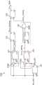
请参照图3,图3是本发明的一实施例中功率因数校正控制器200的电路示意图。如图3所示,在一些实施例中,功率因数校正控制器200包含一模拟数字转换器210、一数字峰值保持电路220、一参考电压产生器230、一误差放大器240及一脉冲宽度调制电路250,其中模拟数字转换器210耦接数字峰值保持电路220,数字峰值保持电路220耦接参考电压产生器230,参考电压产生器230耦接误差放大器240,误差放大器240耦接脉冲宽度调制电路250。以下将详细解释模拟数字转换器210、数字峰值保持电路220、参考电压产生器230、误差放大器240及脉冲宽度调制电路250各自的结构与功能,并说明彼此间的运作方式。Please refer to FIG. 3 . FIG. 3 is a schematic circuit diagram of a power
请参照图4,图4是本发明的一实施例中,功率因数校正控制器200中各元件的输入/输出电压随着时间变化的波形图。如图4所示,在一些实施例中,模拟数字转换器210用以将整流信号VAC(对应于波形W3)转换为一数字输入信号DVAC(对应于波形W4),其中数字输入信号DVAC为一连续的阶梯波形,且数字输入信号DVAC基于一时钟频率以持续更新其数值。如图4的时钟clk及波形W4所示,每经过一个时钟周期,数字输入信号DVAC的值更新一次。模拟数字转换器的结构与功能为本领域技术人员所熟知,故不赘述。Please refer to FIG. 4 . FIG. 4 is a waveform diagram of the input/output voltage of each element in the power
在一些实施例中,数字峰值保持电路220用以根据数字输入信号DVAC而产生一峰值信号DVAC_peak。请参照图5A,图5A是本发明的一实施例中数字峰值保持电路220的模块方块图。如图5A所示,数字峰值保持电路220包含一延迟电路221、一数字上升感测器222、一追踪暂存器223、一数字下降感测器224及一保持暂存器225,其中延迟电路221耦接数字上升感测器222、追踪暂存器223及数字下降感测器224,数字上升感测器222耦接追踪暂存器223,追踪暂存器223耦接保持暂存器225,数字下降感测器224耦接保持暂存器225。以下将详细解释延迟电路221、数字上升感测器222、追踪暂存器223、数字下降感测器224及保持暂存器225各自的结构与功能,并说明彼此间的运作方式。In some embodiments, the digital
在一些实施例中,延迟电路221用以延迟数字输入信号DVAC而产生一延迟输入信号DDVAC,其中延迟输入信号DDVAC延迟于数字输入信号DVAC至少一个时钟周期。如图4所示,在本实施例中,延迟输入信号DDVAC延迟于数字输入信号DVAC一个时钟周期,因此延迟输入信号DDVAC于一第k个时钟周期的值DDVAC[k]等于数字输入信号DVAC于前一个时钟周期,即第k-1个时钟周期的值DVAC[k-1]。其中,k为时钟周期计数值,k-1代表第k个时钟周期的前一个时钟周期。以图4的第1个时钟周期(时间点t1)及波形W4为例,数字输入信号DVAC于第1个时钟周期(时间点t1)的值DVAC[1]为1,而数字输入信号DVAC于前一个时钟周期,即第0个时钟周期(时间点t0)的值DVAC[0]为0,因此延迟输入信号DDVAC于第1个时钟周期(时间点t1)的值DDVAC[1]等于0。需注意的是,延迟输入信号DDVAC延迟于数字输入信号DVAC不限于一个时钟周期,也可以是两个时钟周期、三个时钟周期,或其他多个时钟周期等。In some embodiments, the
在一些实施例中,数字上升感测器222用以比较数字输入信号DVAC及延迟输入信号DDVAC而产生一上升信号DVAC_rising,其中当数字输入信号DVAC于第k个时钟周期的值DVAC[k]大于延迟输入信号DDVAC于第k个时钟周期的值DDVAC[k]时,上升信号DVAC_rising转换为一使能状态(enable)。以图4的时间点t1为例,数字输入信号于第1个时钟周期(时间点t1)的值DVAC[1]为1且延迟输入信号DDVAC于第1个时钟周期(时间点t1)的值DDVAC[1]为0,此时数字输入信号于第k个时钟周期的值DVAC[1]大于延迟输入信号DDVAC于第k个时钟周期的值DDVAC[1],使得上升信号DVAC_rising转换为所述使能状态,其中所述使能状态为一高电位。In some embodiments, the digital rising
在一些实施例中,追踪暂存器223用以于上升信号DVAC_rising为所述使能状态时,闩锁(latch)数字输入信号DVAC的值而产生一追踪信号DVAC_tracking(对应于波形W5)。如图4的波形W4、波形W5所示,当上升信号DVAC_rising为所述使能状态时,追踪暂存器223闩锁数字输入信号DVAC的值而产生追踪信号DVAC_tracking,因此在时段T1中,波形W4与波形W5一致。在一些实施例中,当追踪暂存器223接收一重置信号时,追踪暂存器223将追踪信号DVAC_tracking设定为一重置值,其中追踪信号DVAC_tracking的初始值即为所述重置值。换句话说,追踪暂存器223具有重置功能,使得追踪暂存器223可以将追踪信号DVAC_tracking设定为所述重置值。在一些实施例中,所述重置值为所述禁止状态(即低电位)。In some embodiments, the
在一些实施例中,数字下降感测器224用以比较数字输入信号DVAC及延迟输入信号DDVAC而产生一下降信号DVAC_falling,其中当数字输入信号DVAC于第k个时钟周期(例如时间点t3)的值DVAC[k]小于延迟输入信号DDVAC于第k个时钟周期(时间点t3)的值DDVAC[k]时,下降信号DVAC_falling转换为所述使能状态。以图4的时间点t3为例,时间点t3是数字输入信号DVAC于上升后首次下降的时间点,此时数字输入信号DVAC于时间点t3的值DVAC[k]为5且延迟输入信号DDVAC于时间点t3的值DDVAC[k]为6。由于数字输入信号于时间点t3的值DVAC[k]小于延迟输入信号DDVAC于时间点t3的值DDVAC[k],使得下降信号DVAC_falling转换为所述使能状态。In some embodiments, the digital falling
在一些实施例中,保持暂存器225用以于下降信号DVAC_falling转换为所述使能状态的时点,闩锁追踪信号DVAC_tracking的值而产生峰值信号DVAC_peak(对应于波形W6)。如图4的波形W5、波形W6所示,当下降信号DVAC_falling转换为所述使能状态的时点(例如为时间点t3、时间点t4及时间点t5),保持暂存器225会闩锁追踪信号DVAC_tracking的值而产生峰值信号DVAC_peak。以时间点t3为例,当下降信号DVAC_falling于时间点t3转换为所述使能状态时,保持暂存器225会产生峰值信号DVAC_peak,其中峰值信号DVAC_peak的值等于追踪信号DVAC_tracking于时间点t3的值,因此在时段T2中,峰值信号DVAC_peak的值是闩锁并保持于追踪信号DVAC_tracking于时间点t3的值;又以时间点t4为例,当下降信号DVAC_falling于时间点t4转换为所述使能状态时,保持暂存器225会产生峰值信号DVAC_peak,其中峰值信号DVAC_peak的值等于追踪信号DVAC_tracking于时间点t4的值,因此在时段T3中,峰值信号DVAC_peak的值是闩锁并保持于追踪信号DVAC_tracking于时间点t4的值。In some embodiments, the holding
在一些实施例中,当保持暂存器225接收另一重置信号时,保持暂存器225将峰值信号DVAC_peak设定为另一重置值,其中峰值信号DVAC_peak的初始值即为所述另一重置值。换句话说,保持暂存器225具有重置功能,使得保持暂存器225可以将峰值信号DVAC_peak设定为所述另一重置值。在一些实施例中,所述另一重置值为所述禁止状态(即低电位)。In some embodiments, when the
请参照图5B,图5B是本发明的另一实施例中数字峰值保持电路220的模块方块图。如图5B所示,在一些实施例中,数字峰值保持电路220还包含一保持信号产生器226,其中保持信号产生器226耦接于数字下降感测器224与保持暂存器225之间。保持信号产生器226用以产生一保持信号DVAC_holding,并用以于下降信号DVAC_falling转换为所述使能状态的时点而触发保持信号DVAC_holding的一脉冲(pulse),其中保持暂存器225于所述脉冲的触发时点闩锁追踪信号DVAC_tracking的值而产生峰值信号DVAC_peak的值。Please refer to FIG. 5B , which is a block diagram of a digital
请同时参照图6A及图6B,图6A是本发明的一实施例中数字峰值保持电路220的电路示意图,图6B是本发明的另一实施例中数字峰值保持电路220的电路示意图。如图6A所示,在一些实施例中,延迟电路221为一暂存器Reg,数字上升感测器222由一比较器COM及一D型正反器D-FF所组成,追踪暂存器223为一暂存器Reg,数字下降感测器224由一比较器COM及一D型正反器D-FF所组成,保持暂存器225为一暂存器Reg。如图6B所示,在一些实施例中,保持信号产生器226由一D型正反器D-FF及一与门AND所组成。Please refer to FIG. 6A and FIG. 6B at the same time. FIG. 6A is a schematic circuit diagram of the digital
请同时参照图7A及图7B,图7A及图7B是本发明的另二实施例中数字峰值保持电路220的模块方块图。如图7A及图7B所示,在一些实施例中,数字峰值保持电路220还包含一数字滤波器227,其中数字滤波器227耦接延迟电路221、数字上升感测器222、追踪暂存器223及数字下降感测器224。数字滤波器227用以屏蔽(mask)或过滤(filter)数字输入信号DVAC中的噪声,使得数字输入信号DVAC的值于数字输入信号DVAC的1/2周期或1/4周期内单调递增(monotonically increase)或单调递减(monotonically decrease),进而避免数字输入信号DVAC产生较大的误差值。Please refer to FIG. 7A and FIG. 7B at the same time. FIG. 7A and FIG. 7B are block diagrams of the digital
在一些实施例中,参考电压产生器230用以根据峰值信号DVAC_peak而产生一参考电压Vref,其中参考电压Vref为一定值。一般来说,参考电压Vref具有极佳的稳定性,使其不易受到噪声的影响而导致数值改变。在理想的状况下,参考电压Vref产生之后,维持为一固定的值,且参考电压Vref的值不会受到任何噪声或负载的影响而改变。In some embodiments, the
在一些实施例中,参考电压Vref与峰值信号DVAC_peak之间具有线性(linear)或分段线性(piecewise linear)的一映像关系。请参照图8A,图8A是本发明的一实施例中参考电压Vref与峰值信号DVAC_peak之间的映像关系示意图,其中图8A的横轴所代表的是峰值信号DVAC_peak的值,单位是伏特(V);图8A的纵轴所代表的是参考电压Vref的值,单位是伏特。如图8A所示,图中具有三个分段S1-S3,换句话说,在本实施例中参考电压Vref与峰值信号DVAC_peak之间为分段线性的映像关系。在分段S1中,当峰值信号DVAC_peak的值介于120伏特至170伏特时,参考电压产生器230将参考电压Vref的值映像至210伏特,其中210伏特为本实施例中参考电压Vref的最小值。在分段S2中,当峰值信号DVAC_peak的值介于170伏特至359伏特时,参考电压产生器230将参考电压Vref的值线性地映像至210伏特与400伏特之间。在分段S3中,当峰值信号DVAC_peak的值介于359伏特至375伏特时,参考电压产生器230将参考电压Vref的值映像至400伏特,其中400伏特为本实施例中参考电压Vref的最大值。In some embodiments, there is a linear or piecewise linear mapping relationship between the reference voltage Vref and the peak signal DVAC_peak . Please refer to FIG. 8A. FIG. 8A is a schematic diagram of the image relationship between the reference voltage Vref and the peak signal DVAC_peak in an embodiment of the present invention, wherein the horizontal axis of FIG. 8A represents the value of the peak signal DVAC _peak, and the unit is is volts (V); the vertical axis of FIG. 8A represents the value of the reference voltage Vref, and the unit is volts. As shown in FIG. 8A , there are three segments S1 - S3 in the figure. In other words, in this embodiment, the mapping relationship between the reference voltage Vref and the peak signal DVAC_peak is segmented linear. In segment S1, when the value of the peak signal DVAC_peak is between 120 volts and 170 volts, the
请参照图8B,图8B是本发明的一实施例中参考电压产生器230的示意图。如图8B所示,在一些实施例中,参考电压产生器230包括一查找表231及一数字模拟转换器232,其中查找表231耦接数字模拟转换器232。查找表231用以根据所述映像关系将峰值信号DVAC_peak映像而产生一映像输出信号DVo,数字模拟转换器232则用以将映像输出信号DVo转换为参考电压Vref,其中映像输出信号DVo为一数字信号(digital signal),参考电压Vref为一模拟信号(analog signal)。在一些实施例中,查找表231为一只读存储器(ROM)、一随机存取存储器(RAM)、一闪存(Flash)及其组合所构成的电路。数字模拟转换器232的结构与功能为本领域技术人员所熟知,故不赘述。Please refer to FIG. 8B , which is a schematic diagram of the
在一些实施例中,误差放大器240用以根据反馈信号VFB与参考电压Vref之间的差值而产生一误差放大信号VEOA,其中误差放大器240具有一增益(gain),使得误差放大信号VEOA的值为反馈信号VFB与参考电压Vref之间差值的所述增益倍。举例来说,假设误差放大器240的增益为100,即代表误差放大信号VEOA的值为反馈信号VFB与参考电压Vref之间差值的100倍。在一些实施例中,误差放大器240具有一正相输入端、一反相输入端以及一输出端,其中所述正相输入端用以接收参考电压Vref,所述反相输入端用以接收反馈信号VFB,所述输出端用以输出误差放大信号VEOA。误差放大器240的结构与功能为本领域技术人员所熟知,故不赘述。In some embodiments, the
在一些实施例中,脉冲宽度调制电路250用以对误差放大信号VEOA进行脉冲宽度调制(pulse-width modulation)而产生一驱动信号DRV。脉冲宽度调制是一种将一模拟信号转换为一脉冲信号(pulse signal)的技术,其中当所述模拟信号的值大于一三角波的值或一锯齿波的值时,脉冲宽度调制电路250会输出一高电位状态(例如为1)的驱动信号DRV;当所述模拟信号的值小于所述三角波的值或所述锯齿波的值时,脉冲宽度调制电路250会输出一低电位状态(例如为0)的驱动信号DRV。脉冲宽度调制技术为本领域技术人员所熟知,故不赘述。In some embodiments, the pulse-width modulation circuit 250 is used for performing pulse-width modulation on the error amplifier signal VEOA to generate a driving signal DRV. Pulse width modulation is a technique for converting an analog signal into a pulse signal, wherein when the value of the analog signal is greater than the value of a triangle wave or a sawtooth wave, the pulse width modulation circuit 250 outputs A drive signal DRV in a high potential state (for example, 1); when the value of the analog signal is smaller than the value of the triangle wave or the value of the sawtooth wave, the pulse width modulation circuit 250 will output a low potential state (for example, 0) of the drive signal DRV. The pulse width modulation technology is well known to those skilled in the art, so it will not be described in detail.
在一些实施例中,功率级电路300用以通过一切换电感式转换方法(switchedinductor conversion)将整流电压Vi转换为一输出电压Vo,其中功率级电路300的运作由驱动信号DRV所控制。由于参考电压Vref与峰值信号DVAC_peak之间具有线性或分段线性的映像关系,使得参考电压Vref所对应的输出电压Vo与峰值信号DVAC_peak所对应的整流电压Vi(或交流电压Vac)也具有对应的线性或分段线性的映像关系,在本发明的应用中,输出电压Vo高于整流电压Vi。In some embodiments, the
在一些实施例中,功率级电路300包括至少一电感器、多个开关及至少一电容器,其中所述多个开关可以是二极管(Diode)、双极性晶体管(BJT)或金氧半晶体管(MOSFET)。请参照图9,图9是本发明的一实施例中功率级电路300的电路示意图。如图9所示,功率级电路300例如为一种升压型(boost)功率级电路,例如包括一电感器L1、一二极管D1、一晶体管Q1以及一电容器C1,其中二极管D1及晶体管Q1用以当作开关使用。当驱动信号DRV处于高电位状态时,晶体管Q1被控制而处于一导通状态且二极管D1处于一非导通状态,此时功率级电路300所接收的整流电压Vi会对电感器L1充电;当驱动信号DRV处于低电位状态时,晶体管Q1被控制而处于所述非导通状态且二极管D1处于所述导通状态,此时功率级电路300所接收的整流电压Vi会对电容器C1充电,同时电感器L1也会放电而对电容器C1充电以产生输出电压Vo,以使输出电压Vo高于整流电压Vi。In some embodiments, the
在一些实施例中,反馈电路400用以根据输出电压Vo而产生反馈信号VFB,其中输出电压Vo与反馈信号VFB之间具有一比例关系。在一些实施例中,反馈电路400包括多个电阻器所形成的分压电路,其中各该电阻器的值会影响所述比例关系的值。请参照图10,图10是本发明的一实施例中反馈电路400的电路示意图。如图10所示,在本实施例中,反馈电路400包括二个电阻器R1、R2,其中电阻器R1的值与电阻器R2的值决定输出电压Vo与反馈信号VFB之间的比例关系。举例来说,当电阻器R1的值为4千欧姆(kΩ)且电阻器R2的值为1千欧姆时,输出电压Vo与反馈信号VFB之间的比例关系为5比1,也就是说输出电压Vo的值为反馈信号VFB的值的5倍。In some embodiments, the
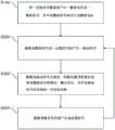
请同时参照图11A至图11C,图11A至图11C是本发明的一实施例中功率因数校正转换器20的控制方法的流程图。如图11A所示,当功率因数校正转换器20开始运作时,功率因数校正转换器20的整流器100将一交流电压Vac整流而产生一整流电压Vi及一整流信号VAC,其中整流信号VAC相关于整流电压Vi(步骤S100)。接着,功率因数校正转换器20的功率因数校正控制器200会根据整流信号VAC及一反馈信号VFB而产生一驱动信号DRV(步骤S200)。随后,功率因数校正转换器20的功率级电路300根据驱动信号DRV并通过一切换电感式转换方法将整流电压Vi转换为一输出电压Vo,其中驱动信号DRV用以控制功率级电路300的一开关的切换以实现所述切换电感式转换方法(步骤S300)。最后,功率因数校正转换器20的反馈电路400会根据输出电压Vo产生反馈信号VFB(步骤S400),使得功率因数校正转换器20重复执行步骤S200至步骤S400。Please refer to FIG. 11A to FIG. 11C at the same time. FIG. 11A to FIG. 11C are flowcharts of a control method of the power
如图11B所示,图11B是功率因数校正控制器200根据整流信号VAC及反馈信号VFB而产生驱动信号DRV的详细流程(即步骤S200的详细流程)。当功率因数校正控制器200接收整流信号VAC及反馈信号VFB时,功率因数校正控制器200的模拟数字转换器210会将整流信号VAC转换为一数字输入信号DVAC(步骤S210)。接着,功率因数校正控制器200的数字峰值保持电路220会根据数字输入信号DVAC而产生一峰值信号DVAC_peak(步骤S220)。随后,功率因数校正控制器200的参考电压产生器230会根据峰值信号DVAC_peak而产生一参考电压Vref(步骤S230),此时功率因数校正控制器200的误差放大器240会根据根据反馈信号VFB与参考电压Vref之间的差值而产生一误差放大信号VEOA(步骤S240)。最后,功率因数校正控制器200的脉冲宽度调制电路250会对误差放大信号VEOA进行脉冲宽度调制而产生驱动信号DRV(步骤S250)。As shown in FIG. 11B , FIG. 11B is a detailed flow of the power
如图11C所示,图11C是数字峰值保持电路220根据数字输入信号DVAC而产生峰值信号DVAC_peak的详细流程(即步骤S220的详细流程)。当数字峰值保持电路220接收数字输入信号DVAC时,数字峰值保持电路220的延迟电路221会延迟数字输入信号DVAC而产生一延迟输入信号DDVAC(步骤S221)。接着,数字峰值保持电路220的数字上升感测器222会比较数字输入信号DVAC及延迟输入信号DDVAC而产生一上升信号DVAC_rising(步骤S222),而当上升信号DVAC_rising转换为一使能状态时,数字峰值保持电路220的追踪暂存器223会闩锁数字输入信号DVAC的值而产生一追踪信号DVAC_tracking(步骤S223);同时,数字峰值保持电路220的数字下降感测器224会比较数字输入信号DVAC及延迟输入信号DDVAC而产生一下降信号DVAC_falling(步骤S224)。最后,当下降信号DVAC_falling转换为所述使能状态时,数字峰值保持电路220的保持暂存器225会闩锁追踪信号DVAC_tracking的值而产生峰值信号DVAC_peak(步骤S225)。As shown in FIG. 11C , FIG. 11C is a detailed flow of the digital
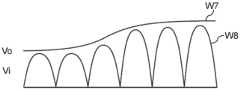
请参照图12,图12是本发明的一实施例中,功率因数校正转换器20中整流电压Vi与输出电压Vo之间的波形比较图,其中波形W7为输出电压Vo的波形,波形W8为整流电压Vi的波形。如图12所示,由于功率因数校正转换器20所输出的输出电压Vo的值跟随整流电压Vi的峰值变化(即波形W7跟随波形W8的峰值变化),使得输出电压Vo与整流电压Vi之间的压差并不大,进而使本实施例的功率因数校正转换器20得以采用尺寸较小的储能元件及开关,以降低功率因数校正转换器20的电路尺寸、成本及运作时的整体功耗。Please refer to FIG. 12. FIG. 12 is a waveform comparison diagram between the rectified voltage Vi and the output voltage Vo in the power
综上所述,相较于图1A与图1B的现有技术,由于本发明的功率因数校正控制器200中设置有数字峰值保持电路220,使得本发明的参考电压Vref被限制在一区间范围内,进而使功率因数校正转换器20所输出的输出电压Vo的值跟随整流电压Vi的峰值变化以降低其二者之间的压差。因此,相较于现有技术,本发明的功率因数校正转换器20有着电路尺寸、成本及其运作时的整体功耗较小的优势存在。此外,由于本发明的功率因数校正转换器20中设置有反馈电路400,使得本发明的功率因数校正转换器20还有着输出电压Vo较稳定的优势存在。To sum up, compared with the prior art shown in FIG. 1A and FIG. 1B , since the power
以上已针对较佳实施例来说明本发明,但以上所述,仅为使本领域技术人员易于了解本发明的内容,并非用来限定本发明的权利范围。所说明的各个实施例,并不限于单独应用,也可以组合应用,举例而言,两个或以上的实施例可以组合运用,而一实施例中的部分组成也可用以取代另一实施例中对应的组成部件。此外,在本发明的相同精神下,本领域技术人员可以想到各种等效变化以及各种组合,举例而言,本发明所称“根据某信号进行处理或运算或产生某输出结果”,不限于根据该信号的本身,也包含于必要时,将该信号进行电压电流转换、电流电压转换、及/或比例转换等,之后根据转换后的信号进行处理或运算产生某输出结果。由此可知,在本发明的相同精神下,本领域技术人员可以想到各种等效变化以及各种组合,其组合方式甚多,在此不一一列举说明。因此,本发明的范围应涵盖上述及其他所有等效变化。The present invention has been described above with reference to preferred embodiments, but the above description is only for those skilled in the art to easily understand the content of the present invention, and is not intended to limit the scope of rights of the present invention. The various embodiments described are not limited to single application, and can also be used in combination. For example, two or more embodiments can be used in combination, and some components in one embodiment can also be used to replace another embodiment. corresponding components. In addition, under the same spirit of the present invention, those skilled in the art can think of various equivalent changes and various combinations. It is limited to the signal itself, and also includes performing voltage-to-current conversion, current-to-voltage conversion, and/or ratio conversion on the signal when necessary, and then processing or computing the converted signal to generate a certain output result. It can be seen that under the same spirit of the present invention, those skilled in the art can think of various equivalent changes and various combinations, and there are many combinations, which will not be listed here. Accordingly, the scope of the invention should encompass the above and all other equivalent variations.
Claims (19)
Translated fromChineseApplications Claiming Priority (2)
| Application Number | Priority Date | Filing Date | Title |
|---|---|---|---|
| US202163277024P | 2021-11-08 | 2021-11-08 | |
| US63/277,024 | 2021-11-08 |
Publications (1)
| Publication Number | Publication Date |
|---|---|
| CN116094307Atrue CN116094307A (en) | 2023-05-09 |
Family
ID=86197964
Family Applications (1)
| Application Number | Title | Priority Date | Filing Date |
|---|---|---|---|
| CN202210695955.8APendingCN116094307A (en) | 2021-11-08 | 2022-06-20 | Power factor correction converter, controller and digital peak hold circuit thereof |
Country Status (2)
| Country | Link |
|---|---|
| CN (1) | CN116094307A (en) |
| TW (1) | TWI824556B (en) |
Family Cites Families (5)
| Publication number | Priority date | Publication date | Assignee | Title |
|---|---|---|---|---|
| US6115273A (en)* | 1998-07-09 | 2000-09-05 | Illinois Tool Works Inc. | Power converter with low loss switching |
| TWI479942B (en)* | 2010-05-12 | 2015-04-01 | Point Somee Ltd Liability Co | Adaptive current regulation for solid state lighting |
| JP5933548B2 (en)* | 2010-08-18 | 2016-06-08 | フィンシックス コーポレイションFinsix Corporation | Ultra high frequency switching cell based power converter |
| US9722487B2 (en)* | 2015-05-11 | 2017-08-01 | Infineon Technologies Ag | Hysteresis controllers for power factor correction in AC/DC power converters |
| US10236763B2 (en)* | 2015-08-04 | 2019-03-19 | Power Integrations, Inc. | Reverse current blockage through buck controller block |
- 2022
- 2022-06-10TWTW111121754Apatent/TWI824556B/enactive
- 2022-06-20CNCN202210695955.8Apatent/CN116094307A/enactivePending
Also Published As
| Publication number | Publication date |
|---|---|
| TWI824556B (en) | 2023-12-01 |
| TW202320464A (en) | 2023-05-16 |
Similar Documents
| Publication | Publication Date | Title |
|---|---|---|
| CN109713889B (en) | Power factor correction circuit and control method thereof | |
| JP6439484B2 (en) | Switching power supply circuit and power factor correction circuit | |
| US10951120B2 (en) | Flyback converter, control circuit and control method therefor | |
| CN110445353B (en) | Digital low-pass filter, power converter, control circuit and driving chip thereof | |
| US9543824B2 (en) | Active power factor correction control circuit, chip and LED driving circuit thereof | |
| KR100829121B1 (en) | Power Factor Correction Circuit for Single Power Operation in BCM Mode | |
| US9385603B2 (en) | Control method and control circuit for switching power supply | |
| US20100259957A1 (en) | Bridgeless pfc circuit for critical continuous current mode and controlling method thereof | |
| TWI575862B (en) | A system controller for adjusting a power converter and a method thereof | |
| US9998005B2 (en) | Single inductor dual output voltage converter and the method thereof | |
| US7352599B2 (en) | Switching power source apparatus | |
| TWI633744B (en) | Control device and control method of Boost PFC converter for quasi-resonant working mode | |
| CN115378248B (en) | Automatic mode switching method and circuit for DC-DC converter | |
| CN107222088B (en) | Control module, switching type power supply device and peak current mode control method | |
| CN100355191C (en) | Controlling circuit, controlling method and sequence generator for dc-dc converter | |
| TWI824556B (en) | Power factor correction converter, controller and digital peak-hold circuit thereof | |
| CN104702092B (en) | Power Factor Correction Circuits for Power Converters | |
| CN109980959A (en) | Method and system based on the peak point current Operation switch power adapter by switch element | |
| CN115833582B (en) | Buck-boost converter, controller and control method thereof | |
| JP2024064507A (en) | Switching control circuit, control circuit, power supply circuit | |
| Tanitteerapan et al. | Simplified input current waveshaping technique by using inductor voltage sensing for high power factor isolated Sepic, Cuk and flyback rectifiers | |
| CN210780542U (en) | Control circuit with high power factor and AC/DC conversion circuit | |
| US20230144791A1 (en) | Power factor correction converter, controller and digital peak-hold circuit thereof | |
| CN116846200B (en) | Control chip and PFC converter | |
| CN114938131B (en) | Control circuit and method of power factor correction circuit based on FLYBACK |
Legal Events
| Date | Code | Title | Description |
|---|---|---|---|
| PB01 | Publication | ||
| PB01 | Publication | ||
| SE01 | Entry into force of request for substantive examination | ||
| SE01 | Entry into force of request for substantive examination |