CN116075005A - Dimming control circuit and LED drive circuit with the same - Google Patents
Dimming control circuit and LED drive circuit with the sameDownload PDFInfo
- Publication number
- CN116075005A CN116075005ACN202111302092.5ACN202111302092ACN116075005ACN 116075005 ACN116075005 ACN 116075005ACN 202111302092 ACN202111302092 ACN 202111302092ACN 116075005 ACN116075005 ACN 116075005A
- Authority
- CN
- China
- Prior art keywords
- dimming
- voltage
- unit
- coupled
- signal
- Prior art date
- Legal status (The legal status is an assumption and is not a legal conclusion. Google has not performed a legal analysis and makes no representation as to the accuracy of the status listed.)
- Granted
Links
Images


Classifications
- H—ELECTRICITY
- H05—ELECTRIC TECHNIQUES NOT OTHERWISE PROVIDED FOR
- H05B—ELECTRIC HEATING; ELECTRIC LIGHT SOURCES NOT OTHERWISE PROVIDED FOR; CIRCUIT ARRANGEMENTS FOR ELECTRIC LIGHT SOURCES, IN GENERAL
- H05B45/00—Circuit arrangements for operating light-emitting diodes [LED]
- H05B45/10—Controlling the intensity of the light
- H—ELECTRICITY
- H05—ELECTRIC TECHNIQUES NOT OTHERWISE PROVIDED FOR
- H05B—ELECTRIC HEATING; ELECTRIC LIGHT SOURCES NOT OTHERWISE PROVIDED FOR; CIRCUIT ARRANGEMENTS FOR ELECTRIC LIGHT SOURCES, IN GENERAL
- H05B45/00—Circuit arrangements for operating light-emitting diodes [LED]
- H05B45/30—Driver circuits
- H05B45/32—Pulse-control circuits
- H05B45/325—Pulse-width modulation [PWM]
- H—ELECTRICITY
- H05—ELECTRIC TECHNIQUES NOT OTHERWISE PROVIDED FOR
- H05B—ELECTRIC HEATING; ELECTRIC LIGHT SOURCES NOT OTHERWISE PROVIDED FOR; CIRCUIT ARRANGEMENTS FOR ELECTRIC LIGHT SOURCES, IN GENERAL
- H05B45/00—Circuit arrangements for operating light-emitting diodes [LED]
- H05B45/50—Circuit arrangements for operating light-emitting diodes [LED] responsive to malfunctions or undesirable behaviour of LEDs; responsive to LED life; Protective circuits
Landscapes
- Circuit Arrangement For Electric Light Sources In General (AREA)
Abstract
Translated fromChinese
Description
Translated fromChinese技术领域technical field
本发明是关于LED驱动装置的技术领域,尤指整合在LED驱动装置内的一种调光控制电路。The invention relates to the technical field of LED driving devices, in particular to a dimming control circuit integrated in the LED driving device.
背景技术Background technique
目前,发光二极管(Light-Emitting Diode,LED)已被广泛地应用于照明装置、背光装置及显示设备。随着LED照明装置市场的快速发展,人们对于LED照明装置产品可靠度、使用寿命与环保节能方面不断要求。此外,人们还要求LED照明装置必须具有可调光功能,其中对于LED照明装置调光功能的要求不仅在于能够达到节能省电的目的,更多的是如何利用调整LED照明装置亮度、色温来获得更佳的生活质量。Currently, light-emitting diodes (Light-Emitting Diode, LED) have been widely used in lighting devices, backlight devices and display devices. With the rapid development of the LED lighting device market, people are constantly demanding the reliability, service life, environmental protection and energy saving of LED lighting device products. In addition, people also require that the LED lighting device must have a dimming function. The requirement for the dimming function of the LED lighting device is not only to achieve the purpose of energy saving and power saving, but also how to use the brightness and color temperature of the LED lighting device to obtain Better quality of life.
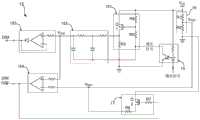
图1显示习知的一种具调光功能的LED驱动电路的电路图。如图1所示,习知技术的具调光功能的LED驱动电路1a可以和一LED发光单元2a一同组成一照明装置,且其基础结构系包括:一直流电压源11a、一输入电容12a、一调光信号产生单元13a、一光耦合器14a、一调光启用/关断电路15a、一开关控制单元16a、一开关组件17a、以及一输出单元18a。进一步地,图2为绘示于图1之中的调光启用/关断电路15a的电路图。如图2所示,习知的调光启用/关断电路15a主要包括:一信号输入单元151a、一直流电压转换单元152a、一第一比较器单元153a、以及一第二比较器单元154a。FIG. 1 shows a circuit diagram of a conventional LED driving circuit with dimming function. As shown in Figure 1, the
使用所述照明装置时,用户可通过操作一调光控制器3a(如:旋钮式控制器或按键式控制器)的方式传送一调光控制信号至所述LED驱动电路1的该调光信号产生单元13a,使该调光信号产生单元13a产生一调光信号(即,PWM信号),从而通过该光耦合器14a将该调光信号传送至该调光启用/关断电路15a。如图2所示,该调光启用/关断电路15a的该信号输入单元151a将所述调光信号进一步地传送至该直流电压转换单元152a,藉由该直流电压转换单元152a将所述调光信号转换成一直流调光电压VDIM。When using the lighting device, the user can transmit a dimming control signal to the dimming signal of the
在习知的LED驱动电路1a中,该第一比较器单元153a依据该直流调光电压VDIM而产生一第一比较信号DIM,且将该第一比较信号DIM传送至该开关控制单元16a(如图1所示)。另一方面,该第二比较器单元154a依据该直流调光电压VDIM以及通过一分压电阻器19a所接收的一参考电压VREF而产生一第二比较信号DIM_OFF,且将该第二比较信号DIM_OFF传送至该开关控制单元16a(如图1所示)。In the conventional
如图1所示,开关组件17a工作的汲极电流直接影响流经LED发光单元2a的电流,而流经LED发光单元2a的电流即为LED驱动电路1a的输出电流。因此,对于使用第一比较器单元153a和第二比较器单元154a实现调光功能的LED驱动电路1a而言,若调光控制器2a输入的调光控制信号最终使LED驱动电路1a的输出电流在开启、关闭的断点附近时,则容易出现输出电流在开启、关闭断点附近出现频繁切换的问题,导致人眼看见灯闪。As shown in FIG. 1 , the drain current of the
为了解决人眼看见灯闪的问题,如图1与图2所示,习知技术是通过加入一个兆奥姆(MΩ)级别的电阻RF的方式,将第二比较器单元154a设计成一迟滞比较器电路。如此设计,可以将开启和关闭的断点之间的距离拉长,解决了灯闪问题。可惜的是,此解决方案无法精确地计算开启和关闭的断点之间的距离。同时,在所述调光启用/关断电路15a被芯片化之后,开启和关闭的断点之间的距离便无法随意更改。In order to solve the problem that the human eye sees the light flickering, as shown in Fig. 1 and Fig. 2, the conventional technology is to design the
由上述说明可知,习知技术具调光功能的LED驱动电路1a显然仍具有加以改善的空间。有鉴于此,本案发明人极力加以研究发明,而终于研发完成一种调光控制电路。From the above description, it can be seen that the conventional
发明内容Contents of the invention
本发明主要目的在于提供一种调光控制电路,其主要包括:一参考电压提供单元、一调光启用/关断电路以及一调整单元。正常工作时,该调光启用/关断电路依据一调光信号(如:PWM信号)而产生且传送一第一比较信号和一第二比较信号至LED驱动电路之中的一开关控制单元。并且,在由该调光信号转换而成的一直流调光电压大于参考电压的情况下,该第二比较信号为具有一第一准位(H或L),且该第二比较信号在该直流调光电压小于该参考电压时具有一第二准位(L或H)。依据本发明的设计,在该参考电压低于该直流调光电压的情况下,该调整单元启用以拉低该参考电压的电压值,使得调光关断时所需的直流调光电压相较于调光开启时所需的直流调光电压来的更低,从而实现调光开启和调光关闭之间的迟滞。如此设计,可以将调光开启和关闭的断点之间的距离拉长,解决了灯闪问题。The main purpose of the present invention is to provide a dimming control circuit, which mainly includes: a reference voltage supply unit, a dimming enabling/disabling circuit and an adjusting unit. When working normally, the dimming enable/disable circuit generates according to a dimming signal (such as: PWM signal) and transmits a first comparison signal and a second comparison signal to a switch control unit in the LED driving circuit. Moreover, when a DC dimming voltage converted from the dimming signal is greater than the reference voltage, the second comparison signal has a first level (H or L), and the second comparison signal is at the When the DC dimming voltage is lower than the reference voltage, it has a second level (L or H). According to the design of the present invention, when the reference voltage is lower than the DC dimming voltage, the adjustment unit is activated to pull down the voltage value of the reference voltage, so that the required DC dimming voltage is lower than the The required DC dimming voltage is lower when the dimming is turned on, so as to realize the hysteresis between dimming on and dimming off. With such a design, the distance between the breakpoints of dimming on and off can be lengthened, which solves the problem of light flickering.
因此,对于调光控制电路的开发者而言,其仅需调整参考电压提供单元以变更该参考电压的电压值,即可自行变更调光开启和关闭的断点之间的距离。Therefore, for the developer of the dimming control circuit, he only needs to adjust the reference voltage supply unit to change the voltage value of the reference voltage, and he can change the distance between the dimming on and off breakpoints by himself.
为达成上述目的,本发明提出所述调光控制电路的一第一实施例,其应用于整合在一LED照明装置所具有的一LED驱动电路之中,且包括:To achieve the above object, the present invention proposes a first embodiment of the dimming control circuit, which is applied to be integrated in an LED driving circuit of an LED lighting device, and includes:
一参考电压提供单元,具有一第一端、一第二端与一电压提供端,其中该一第一端和一第二端分别耦接一工作电压与一接地端;A reference voltage supply unit having a first terminal, a second terminal and a voltage supply terminal, wherein the first terminal and the second terminal are respectively coupled to a working voltage and a ground terminal;
一调光启用/关断电路,耦接一调光信号、该工作电压与该接地端,且耦接该参考电压提供单元的该电压提供端以接收一参考电压,且包括:A dimming enable/disable circuit, coupled to a dimming signal, the operating voltage and the ground terminal, and coupled to the voltage supply terminal of the reference voltage supply unit to receive a reference voltage, and includes:
一直流电压转换单元,耦接该调光信号与该接地端,用以将该调光信号转换成一直流调光电压;a DC voltage conversion unit, coupled to the dimming signal and the ground terminal, for converting the dimming signal into a DC dimming voltage;
一第一比较器单元,耦接该直流电压转换单元以接收该直流调光电压,且依据该直流调光电压而产生一第一比较信号,从而以其一输出端传送该第一比较信号至该LED驱动电路之中的一开关控制单元;以及,A first comparator unit, coupled to the DC voltage conversion unit to receive the DC dimming voltage, and generate a first comparison signal according to the DC dimming voltage, so as to transmit the first comparison signal to the a switch control unit in the LED driving circuit; and,
一第二比较器单元,耦接该直流电压转换单元以接收该直流调光电压,且同时耦接该参考电压提供单元的该电压提供端以接收所述参考电压,其中该第二比较器单元依据该直流调光电压和该参考电压而产生一第二比较信号,从而以其一输出端传送该第二比较信号至该LED驱动电路的该开关控制单元;以及,A second comparator unit, coupled to the DC voltage conversion unit to receive the DC dimming voltage, and coupled to the voltage supply end of the reference voltage supply unit to receive the reference voltage, wherein the second comparator unit generating a second comparison signal according to the DC dimming voltage and the reference voltage, so as to transmit the second comparison signal to the switch control unit of the LED driving circuit through an output terminal thereof; and,
一调整单元,具有一第一电性端、一第二电性端与一第三电性端,其中该第一电性端耦接该第二比较器单元的该输出端,该第二电性端耦接该接地端,且该第三电性端耦接该参考电压提供单元的该电压提供端以接收所述参考电压;An adjusting unit has a first electrical terminal, a second electrical terminal and a third electrical terminal, wherein the first electrical terminal is coupled to the output terminal of the second comparator unit, and the second electrical terminal is coupled to the output terminal of the second comparator unit. The ground terminal is coupled to the ground terminal, and the third electrical terminal is coupled to the voltage supply terminal of the reference voltage supply unit to receive the reference voltage;
其中,在该直流调光电压大于该参考电压的情况下,该第二比较信号具有高准位,且该第二比较信号在该直流调光电压小于该参考电压时具有低准位;Wherein, when the DC dimming voltage is greater than the reference voltage, the second comparison signal has a high level, and the second comparison signal has a low level when the DC dimming voltage is lower than the reference voltage;
其中,在该参考电压低于该直流调光电压的情况下,该调整单元启用以拉低该参考电压的电压值。Wherein, when the reference voltage is lower than the DC dimming voltage, the adjustment unit is enabled to pull down the voltage value of the reference voltage.
并且,本发明同时提出所述调光控制电路的一第二实施例,其应用于整合在一LED照明装置所具有的一LED驱动电路之中,且包括:Moreover, the present invention also proposes a second embodiment of the dimming control circuit, which is applied to be integrated in an LED driving circuit of an LED lighting device, and includes:
一参考电压提供单元,具有一第一端、一第二端与一电压提供端,其中该一第一端和一第二端分别耦接一工作电压与一接地端;A reference voltage supply unit having a first terminal, a second terminal and a voltage supply terminal, wherein the first terminal and the second terminal are respectively coupled to a working voltage and a ground terminal;
一调光启用/关断电路,耦接一调光信号、该工作电压与该接地端,且耦接该参考电压提供单元的该电压提供端以接收一参考电压,且包括:A dimming enable/disable circuit, coupled to a dimming signal, the operating voltage and the ground terminal, and coupled to the voltage supply terminal of the reference voltage supply unit to receive a reference voltage, and includes:
一直流电压转换单元,耦接该调光信号与该接地端,用以将该调光信号转换成一直流调光电压;a DC voltage conversion unit, coupled to the dimming signal and the ground terminal, for converting the dimming signal into a DC dimming voltage;
一第一比较器单元,耦接该直流电压转换单元以接收该直流调光电压,且依据该直流调光电压而产生一第一比较信号,从而以其一输出端传送该第一比较信号至该LED驱动电路之中的一开关控制单元;以及,A first comparator unit, coupled to the DC voltage conversion unit to receive the DC dimming voltage, and generate a first comparison signal according to the DC dimming voltage, so as to transmit the first comparison signal to the a switch control unit in the LED driving circuit; and,
一第二比较器单元,耦接该直流电压转换单元以接收该直流调光电压,且同时耦接该参考电压提供单元的该电压提供端以接收所述参考电压,其中该第二比较器单元依据该直流调光电压和该参考电压而产生一第二比较信号,从而以其一输出端传送该第二比较信号至该LED驱动电路的该开关控制单元;以及,A second comparator unit, coupled to the DC voltage conversion unit to receive the DC dimming voltage, and coupled to the voltage supply end of the reference voltage supply unit to receive the reference voltage, wherein the second comparator unit generating a second comparison signal according to the DC dimming voltage and the reference voltage, so as to transmit the second comparison signal to the switch control unit of the LED driving circuit through an output terminal thereof; and,
一调整单元,具有一第一电性端、一第二电性端与一第三电性端,其中该第一电性端耦接该第二比较器单元的该输出端,该第二电性端耦接该工作电压,且该第三电性端耦接该参考电压提供单元的该电压提供端以接收所述参考电压;An adjusting unit has a first electrical terminal, a second electrical terminal and a third electrical terminal, wherein the first electrical terminal is coupled to the output terminal of the second comparator unit, and the second electrical terminal is coupled to the output terminal of the second comparator unit. The polarity terminal is coupled to the working voltage, and the third electrical terminal is coupled to the voltage supply terminal of the reference voltage supply unit to receive the reference voltage;
其中,在该直流调光电压大于该参考电压的情况下,该第二比较信号具有低准位,且该第二比较信号在该直流调光电压小于该参考电压时具有高准位;Wherein, when the DC dimming voltage is greater than the reference voltage, the second comparison signal has a low level, and the second comparison signal has a high level when the DC dimming voltage is lower than the reference voltage;
其中,在该直流调光电压大于该参考电压的情况下,该调整单元启用以拉低该参考电压的电压值。Wherein, when the direct current dimming voltage is greater than the reference voltage, the adjustment unit is enabled to pull down the voltage value of the reference voltage.
在可行的实施例中,该参考电压提供单元为包括一第一电阻与一第二电阻的一分压电阻器。In a feasible embodiment, the reference voltage providing unit is a voltage dividing resistor including a first resistor and a second resistor.
在可行的实施例中,该直流电压转换单元为一二阶RC滤波器。In a feasible embodiment, the DC voltage conversion unit is a second-order RC filter.
在可行的实施例中,该调光启用/关断电路更包括耦接于该调光信号与该直流电压转换单元之间的一信号输入单元,其包括:In a feasible embodiment, the dimming enable/disable circuit further includes a signal input unit coupled between the dimming signal and the DC voltage conversion unit, which includes:
一第一MOS晶体管,其一源极端耦接该工作电压;a first MOS transistor, one source terminal of which is coupled to the working voltage;
一第三电阻,耦接于该第一MOS晶体管的一汲极端与该接地端之间;a third resistor coupled between a drain terminal of the first MOS transistor and the ground terminal;
一第四电阻,耦接于该第一MOS晶体管的一闸极端与该工作电压之间;以及,a fourth resistor coupled between a gate terminal of the first MOS transistor and the operating voltage; and,
一第五电阻,耦接于该第一MOS晶体管的该闸极端与该接地端之间;a fifth resistor, coupled between the gate terminal of the first MOS transistor and the ground terminal;
其中,该直流电压转换单元具有一第一端、一第二端与一第三端,该第一端耦接至该第三电阻与该第一MOS晶体管的该汲极端之间的一共接点,该第二端用以提供所述直流调光电压至该第一比较器单元,且该第三端耦接该接地端。Wherein, the DC voltage conversion unit has a first terminal, a second terminal and a third terminal, the first terminal is coupled to a common point between the third resistor and the drain terminal of the first MOS transistor, The second terminal is used to provide the DC dimming voltage to the first comparator unit, and the third terminal is coupled to the ground terminal.
在可行的实施例中,该调整单元包括:In a feasible embodiment, the adjustment unit includes:
一第二MOS晶体管,其一源极端耦接该接地端;a second MOS transistor, a source terminal of which is coupled to the ground terminal;
一第六电阻,耦接于该第二MOS晶体管的一汲极端与该参考电压提供单元的该电压提供端之间;以及,a sixth resistor coupled between a drain terminal of the second MOS transistor and the voltage supply terminal of the reference voltage supply unit; and,
一第七电阻,耦接于该第二MOS晶体管的一闸极端与该第二比较器单元的该输出端之间。A seventh resistor is coupled between a gate terminal of the second MOS transistor and the output terminal of the second comparator unit.
在该LED驱动电路之中,一调光信号产生单元接收发送自一调光控制器的一调光控制信号,且将该调光控制信号转换成一调光信号,该调光信号通过一光耦合器传送至该调光启用/关断电路的该信号输入单元,使该直流电压转换单元通过所述信号输入单元接收该调光信号。In the LED driving circuit, a dimming signal generating unit receives a dimming control signal sent from a dimming controller, and converts the dimming control signal into a dimming signal, and the dimming signal is passed through an optical coupling The signal input unit of the dimming enabling/disabling circuit is transmitted to the signal input unit of the dimming enable/disable circuit, so that the DC voltage conversion unit receives the dimming signal through the signal input unit.
在一实施例中,该调光信号为一PWM信号。In one embodiment, the dimming signal is a PWM signal.
进一步地,本发明同时揭示一种LED驱动电路,具有如前所述本发明的调光控制电路。Further, the present invention also discloses an LED driving circuit, which has the dimming control circuit of the present invention as mentioned above.
附图说明Description of drawings
图1为习知的一种具调光功能的LED驱动电路的电路图;Fig. 1 is a circuit diagram of a known LED drive circuit with dimming function;
图2为绘示于图1之中的调光启用/关断电路的电路图;FIG. 2 is a circuit diagram of the dimming enable/disable circuit shown in FIG. 1;
图3为包含本发明一种调光控制电路的一LED驱动电路的第一电路图;3 is a first circuit diagram of an LED drive circuit including a dimming control circuit of the present invention;
图4为绘示于图3之中的调光启用/关断电路的电路图;FIG. 4 is a circuit diagram of the dimming enable/disable circuit shown in FIG. 3;
图5为包含本发明一种调光控制电路的一LED驱动电路的第二电路图;以及,5 is a second circuit diagram of an LED driving circuit including a dimming control circuit of the present invention; and,
图6为绘示于图5之中的调光启用/关断电路的电路图。FIG. 6 is a circuit diagram of the dimming enable/disable circuit shown in FIG. 5 .
附图标记说明:Explanation of reference signs:
1a:LED驱动电路1a: LED drive circuit
11a:直流电压源11a: DC voltage source
12a:输入电容12a: Input capacitance
13a:调光信号产生单元13a: Dimming signal generation unit
14a:光耦合器14a: Optical coupler
15a:调光启用/关断电路15a: Dimming enable/shutdown circuit
151a:信号输入单元151a: Signal input unit
152a:直流电压转换单元152a: DC voltage conversion unit
153a:第一比较器单元153a: first comparator unit
154a:第二比较器单元154a: second comparator unit
RF:电阻RF : Resistance
16a:开关控制单元16a: Switch control unit
17a:开关组件17a: switch assembly
18a:输出单元18a: Output unit
19a:分压电阻器19a: Divider resistor
2a:LED发光单元2a: LED lighting unit
3a:调光控制器3a: Dimming controller
1:LED驱动电路1: LED drive circuit
11:直流电压源11: DC voltage source
12:输入电容12: Input capacitance
13:调光信号产生单元13: Dimming signal generating unit
14:光耦合器14: Optocoupler
15:调光启用/关断电路15: Dimming enable/shutdown circuit
151:信号输入单元151: Signal input unit
152:直流电压转换单元152: DC voltage conversion unit
153:第一比较器单元153: The first comparator unit
154:第二比较器单元154: The second comparator unit
16:开关控制单元16: Switch control unit
17:开关组件17: switch assembly
18:输出单元18: Output unit
19:参考电压提供单元19: Reference voltage supply unit
1T:调整单元1T: adjustment unit
2:LED发光单元2: LED lighting unit
3:调光控制器3: Dimming controller
R1:第一电阻R1: the first resistor
R2:第二电阻R2: Second resistor
R3:第三电阻R3: the third resistor
R4:第四电阻R4: the fourth resistor
R5:第五电阻R5: Fifth resistor
R6:第六电阻R6: the sixth resistor
R7:第七电阻R7: The seventh resistor
Q1:第一MOS晶体管Q1: First MOS transistor
Q2:第二MOS晶体管Q2: Second MOS transistor
具体实施方式Detailed ways
为了能够更清楚地描述本发明所提出一种调光控制电路及具有该调光电路的LED驱动电路,以下将配合图式,详尽说明本发明的较佳实施例。In order to more clearly describe the dimming control circuit and the LED driving circuit with the dimming circuit provided by the present invention, preferred embodiments of the present invention will be described in detail below with reference to the drawings.
第一实施例first embodiment
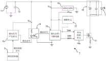
图3显示包含本发明一种调光控制电路的一LED驱动电路的第一电路图。如图3所示,LED驱动电路1可以和一LED发光单元2一同组成一照明装置,且其基础结构系包括:一直流电压源11、一输入电容12、一开关控制单元16(受控于一回授控制器,图中未显示)、一开关组件17、以及一输出单元18。长期涉及LED驱动电路设计与制造的电子工程师必然知道,绘示于图3之中的直流电压源11可为一交流-直流转换器或一直流-直流转换器。进一步地,将本发明一种调光控制电路及一调光控制器3与该LED驱动电路1进行整合之后,所述照明装置即具有可调光功能。如图3所示,本发明一种调光控制电路包括:一调光信号产生单元13、一光耦合器14、一参考电压提供单元19、一调光启用/关断电路15、以及一调整单元1T。继续地参阅图3,并请同时参阅图4,其为绘示于图3之中的调光启用/关断电路15的电路图。如图4所示,该调光启用/关断电路15主要包括:一信号输入单元151、一直流电压转换单元152、一第一比较器单元153、以及一第二比较器单元154。其中,该参考电压提供单元19为包括一第一电阻R1与一第二电阻R2的一分压电阻器,且其具有一第一端、一第二端与一电压提供端,其中该一第一端和一第二端分别耦接一工作电压VCC与一接地端。FIG. 3 shows a first circuit diagram of an LED driving circuit including a dimming control circuit of the present invention. As shown in Figure 3, the
更详细地说明,使用此具有调光功能的照明装置时,用户可通过操作该调光控制器3(如:旋钮式控制器或按键式控制器)的方式传送一调光控制信号至该调光信号产生单元13。接着,该调光信号产生单元13将该调光控制信号转换成一调光信号,且通过该光耦合器14将该调光信号传送至该调光启用/关断电路15的该信号输入单元151,使该直流电压转换单元152通过所述信号输入单元151接收该调光信号。如图4所示,在可行的实施例中,该信号输入单元151耦接于该调光信号与该直流电压转换单元152之间,且其包括:一第一MOS晶体管Q1、一第三电阻R3、一第四电阻R4、以及一第五电阻R5。(由于专利前案没有揭示,因此发明人可以在此进一步地补充由Q1、R3~R5组成信号输入单元151的功用)To explain in more detail, when using this lighting device with dimming function, the user can send a dimming control signal to the dimming
承上述说明,该第一MOS晶体管Q1的源极端耦接该工作电压VCC,该第三电阻R3耦接于该第一MOS晶体管Q1的汲极端与该接地端之间,该第四电阻R4耦接于该第一MOS晶体管Q1的闸极端与该工作电压VCC之间,且该第五电阻R5耦接于该第一MOS晶体管Q1的该闸极端与该接地端之间。并且,依据本发明设计,该直流电压转换单元152为一二阶RC滤波器,用以将所述调光信号(如,PWM信号)转换成一直流调光电压VDIM,且其具有一第一端、一第二端与一第三端,其中该第一端耦接至该第三电阻R3与该第一MOS晶体管Q1的该汲极端之间的一共接点,该第二端用以提供所述直流调光电压VDIM至该第一比较器单元153,且该第三端耦接该接地端。According to the above description, the source terminal of the first MOS transistor Q1 is coupled to the working voltage VCC , the third resistor R3 is coupled between the drain terminal of the first MOS transistor Q1 and the ground terminal, and the fourth resistor R4 The fifth resistor R5 is coupled between the gate terminal of the first MOS transistor Q1 and the working voltage VCC , and the fifth resistor R5 is coupled between the gate terminal of the first MOS transistor Q1 and the ground terminal. Moreover, according to the design of the present invention, the DC
如图3与图4所示,该第一比较器单元153耦接该直流电压转换单元152以接收该直流调光电压VDIM,且依据该直流调光电压VDIM而产生一第一比较信号DIM,从而以其一输出端传送该第一比较信号DIM至该开关控制单元16。另一方面,该第二比较器单元154耦接该直流电压转换单元152以接收该直流调光电压VDIM,且同时耦接该参考电压提供单元19的该电压提供端以接收所述参考电压VREF。如此设置,该第二比较器单元154依据该直流调光电压VDIM和该参考电压VREF而产生一第二比较信号DIM_OFF,从而以其一输出端传送该第二比较信号DIM_OF至该开关控制单元16。As shown in FIG. 3 and FIG. 4 , the
在第一实施例中,该调整单元1T由一第二MOS晶体管Q2、一第六电阻R6以及一第七电阻R7组成,且具有用以对外连接的一第一电性端、一第二电性端与一第三电性端。如图3与图4所示,该第一电性端耦接该第二比较器单元154的该输出端,该第二电性端耦接该接地端,且该第三电性端耦接该参考电压提供单元19的该电压提供端以接收所述参考电压VREF。更详细地说明,在该调整单元1T之中,该第二MOS晶体管Q2的源极端耦接该接地端,该第六电阻R6耦接于该第二MOS晶体管Q2的汲极端与该参考电压提供单元19的该电压提供端之间,且该第七电阻R7耦接于该第二MOS晶体管Q2的闸极端与该第二比较器单元152的该输出端之间。In the first embodiment, the
正常工作时,如图4所示,在该直流调光电压VDIM大于该参考电压VREF的情况下,该第二比较信号DIM_OFF具有高准位,此时调光启用。相反地,该第二比较信号DIM_OFF在该直流调光电压VDIM小于该参考电压VREF时具有低准位,此时调光关闭。为了调光开启和关闭的断点之间的距离拉长以解决灯闪问题,本发明设计了由一第二MOS晶体管Q2、一第六电阻R6以及一第七电阻R7组成的调整单元1T。如图4所示,在该参考电压VREF低于该直流调光电压VDIM的情况下,该调整单元1T启用以拉低该参考电压VREF的电压值。During normal operation, as shown in FIG. 4 , when the DC dimming voltage VDIM is greater than the reference voltage VREF , the second comparison signal DIM_OFF has a high level, and dimming is enabled at this time. Conversely, the second comparison signal DIM_OFF has a low level when the DC dimming voltage VDIM is lower than the reference voltage VREF , and the dimming is turned off at this time. In order to lengthen the distance between the breakpoints of dimming on and off to solve the problem of light flickering, the present invention designs an
更详细地说明,如图4所示,第二MOS晶体管Q2的源极端耦接该接地端,且第二MOS晶体管Q2的汲极端通过该第六电阻R6而耦接至该参考电压提供单元19的该电压提供端。因此,当第二比较信号DIM_OFF具有低准位时(即,VDIM>VREF),由该参考电压提供单元19的该电压提供端所输出的参考电压VREF会因为第二MOS晶体管Q2的导通而被拉低电压值。在此情况下,对于该第二第二比较器单元154而言,调光关断时所需的直流调光电压相较于调光开启时所需的直流调光电压来的更低,从而实现调光开启和调光关闭之间的迟滞。如此设计,便可以将调光开启和关闭的断点之间的距离拉长,解决了灯闪问题。In more detail, as shown in FIG. 4, the source terminal of the second MOS transistor Q2 is coupled to the ground terminal, and the drain terminal of the second MOS transistor Q2 is coupled to the reference
第二实施例second embodiment
图5显示包含本发明一种调光控制电路的一LED驱动电路的第二电路图。如图5所示,在第二实施例中,LED驱动电路1可以和一LED发光单元2一同组成一照明装置,且其基础结构系包括:一直流电压源11、一输入电容12、一开关控制单元16(受控于一回授控制器,图中未显示)、一开关组件17、以及一输出单元18。进一步地,将本发明一种调光控制电路及一调光控制器3与该LED驱动电路1进行整合之后,所述照明装置即具有可调光功能。FIG. 5 shows a second circuit diagram of an LED driving circuit including a dimming control circuit of the present invention. As shown in Figure 5, in the second embodiment, the
如图5所示,本发明一种调光控制电路包括:一调光信号产生单元13、一光耦合器14、一参考电压提供单元19、一调光启用/关断电路15、以及一调整单元1T。继续地参阅图5,并请同时参阅图6,其为绘示于图5之中的调光启用/关断电路15的电路图。如图4所示,该调光启用/关断电路15主要包括:一信号输入单元151、一直流电压转换单元152、一第一比较器单元153、以及一第二比较器单元154。As shown in FIG. 5 , a dimming control circuit of the present invention includes: a dimming
在比较图5和图3以及图6和图4之后,电子工程师可以轻易地理解,在第二实施例中,该调整单元1T同样是由一第二MOS晶体管Q2、一第六电阻R6以及一第七电阻R7组成,且具有用以对外连接的一第一电性端、一第二电性端与一第三电性端。然而,与前述第一实施例不同的是,该第一电性端耦接该第二比较器单元154的该输出端,该第二电性端耦接该工作电压VCC,且该第三电性端耦接该参考电压提供单元19的该电压提供端以接收所述参考电压VREF。更详细地说明,在该调整单元1T之中,该第二MOS晶体管Q2的源极端耦接该该参考电压VREF,该第六电阻R6耦接于该第二MOS晶体管Q2的汲极端与该工作电压VCC之间,且该第七电阻R7耦接于该第二MOS晶体管Q2的闸极端与该第二比较器单元152的该输出端之间。After comparing Fig. 5 and Fig. 3 and Fig. 6 and Fig. 4, electronic engineers can easily understand that in the second embodiment, the
正常工作时,如图6所示,在该直流调光电压VDIM大于该参考电压VREF的情况下,该第二比较信号DIM_OFF具有低准位,此时调光启用。相反地,该第二比较信号DIM_OFF在该直流调光电压VDIM小于该参考电压VREF时具有高准位,此时调光关闭。为了调光开启和关闭的断点之间的距离拉长以解决灯闪问题,本发明设计了由一第二MOS晶体管Q2、一第六电阻R6以及一第七电阻R7组成的调整单元1T。如图6所示,在该直流调光电压VDIM大于该参考电压VREF的情况下,该调整单元1T启用以拉低该参考电压VREF的电压值。During normal operation, as shown in FIG. 6 , when the DC dimming voltage VDIM is greater than the reference voltage VREF , the second comparison signal DIM_OFF has a low level, and dimming is enabled at this time. Conversely, the second comparison signal DIM_OFF has a high level when the DC dimming voltage VDIM is lower than the reference voltage VREF , and the dimming is turned off at this time. In order to lengthen the distance between the breakpoints of dimming on and off to solve the problem of light flickering, the present invention designs an
更详细地说明,如图6所示,第二MOS晶体管Q2的源极端耦接该参考电压VREF,且第二MOS晶体管Q2的汲极端通过该第六电阻R6而耦接至该工作电压VCC。因此,当第二比较信号DIM_OFF具有低准位时(即,VDIM>VREF),由该参考电压提供单元19的该电压提供端所输出的参考电压VREF会因为第二MOS晶体管Q2的关断而被拉低电压值。在此情况下,对于该第二第二比较器单元154而言,调光关断时所需的直流调光电压相较于调光开启时所需的直流调光电压来的更低,从而实现调光开启和调光关闭之间的迟滞。如此设计,便可以将调光开启和关闭的断点之间的距离拉长,解决了灯闪问题。In more detail, as shown in FIG. 6 , the source terminal of the second MOS transistor Q2 is coupled to the reference voltage VREF , and the drain terminal of the second MOS transistor Q2 is coupled to the operating voltage V through the sixth resistor R6.CC . Therefore, when the second comparison signal DIM_OFF has a low level (that is, VDIM >VREF ), the reference voltage VREF output by the voltage supply end of the reference
如此,上述已完整且清楚地说明本发明一种调光控制电路及具有该调光电路的LED驱动电路。然而,必须加以强调的是,前述本案所揭示者乃为较佳实施例,举凡局部的变更或修饰而源于本案的技术思想而为熟习该项技艺之人所易于推知者,俱不脱本案的专利权范畴。Thus, the above has completely and clearly described a dimming control circuit and an LED driving circuit having the dimming circuit of the present invention. However, it must be emphasized that what is disclosed in the above-mentioned case is a preferred embodiment, and all partial changes or modifications derived from the technical ideas of this case and easily deduced by those who are familiar with the art will not deviate from this case. scope of patent rights.
Claims (16)
Priority Applications (1)
| Application Number | Priority Date | Filing Date | Title |
|---|---|---|---|
| CN202111302092.5ACN116075005B (en) | 2021-11-04 | 2021-11-04 | Dimming control circuit and LED driving circuit having the same |
Applications Claiming Priority (1)
| Application Number | Priority Date | Filing Date | Title |
|---|---|---|---|
| CN202111302092.5ACN116075005B (en) | 2021-11-04 | 2021-11-04 | Dimming control circuit and LED driving circuit having the same |
Publications (2)
| Publication Number | Publication Date |
|---|---|
| CN116075005Atrue CN116075005A (en) | 2023-05-05 |
| CN116075005B CN116075005B (en) | 2025-05-02 |
Family
ID=86182585
Family Applications (1)
| Application Number | Title | Priority Date | Filing Date |
|---|---|---|---|
| CN202111302092.5AActiveCN116075005B (en) | 2021-11-04 | 2021-11-04 | Dimming control circuit and LED driving circuit having the same |
Country Status (1)
| Country | Link |
|---|---|
| CN (1) | CN116075005B (en) |
Citations (9)
| Publication number | Priority date | Publication date | Assignee | Title |
|---|---|---|---|---|
| CN101001497A (en)* | 2006-01-12 | 2007-07-18 | 普诚科技股份有限公司 | Light regulating system, control device and method of fluorescent lamp |
| WO2009119617A1 (en)* | 2008-03-24 | 2009-10-01 | 東芝ライテック株式会社 | Electric power device, and lighting fixture |
| TW201203207A (en)* | 2009-11-24 | 2012-01-16 | Samsung Electronics Co Ltd | Method of controlling supply voltage, multi-channel light-emitting diode driving circuit and multi-channel system using the same |
| CN102740541A (en)* | 2011-04-15 | 2012-10-17 | 登丰微电子股份有限公司 | conversion controller |
| CN102958240A (en)* | 2011-08-19 | 2013-03-06 | 盛群半导体股份有限公司 | light source device and dimming control circuit thereof |
| CN105992436A (en)* | 2015-02-13 | 2016-10-05 | 台达电子工业股份有限公司 | LED driving device and control method thereof |
| CN107301849A (en)* | 2017-07-19 | 2017-10-27 | 深圳市华星光电半导体显示技术有限公司 | Display driver chip and liquid crystal display device |
| US20180054865A1 (en)* | 2016-08-22 | 2018-02-22 | Fairchild Korea Semiconductor Ltd. | Hybrid dimming for lighting circuits |
| TWI658748B (en)* | 2017-12-13 | 2019-05-01 | Leadtrend Technology Corporation | Dimming controller capable of receiving pulse width modulation signal and DC signal and related dimming method |
- 2021
- 2021-11-04CNCN202111302092.5Apatent/CN116075005B/enactiveActive
Patent Citations (9)
| Publication number | Priority date | Publication date | Assignee | Title |
|---|---|---|---|---|
| CN101001497A (en)* | 2006-01-12 | 2007-07-18 | 普诚科技股份有限公司 | Light regulating system, control device and method of fluorescent lamp |
| WO2009119617A1 (en)* | 2008-03-24 | 2009-10-01 | 東芝ライテック株式会社 | Electric power device, and lighting fixture |
| TW201203207A (en)* | 2009-11-24 | 2012-01-16 | Samsung Electronics Co Ltd | Method of controlling supply voltage, multi-channel light-emitting diode driving circuit and multi-channel system using the same |
| CN102740541A (en)* | 2011-04-15 | 2012-10-17 | 登丰微电子股份有限公司 | conversion controller |
| CN102958240A (en)* | 2011-08-19 | 2013-03-06 | 盛群半导体股份有限公司 | light source device and dimming control circuit thereof |
| CN105992436A (en)* | 2015-02-13 | 2016-10-05 | 台达电子工业股份有限公司 | LED driving device and control method thereof |
| US20180054865A1 (en)* | 2016-08-22 | 2018-02-22 | Fairchild Korea Semiconductor Ltd. | Hybrid dimming for lighting circuits |
| CN107301849A (en)* | 2017-07-19 | 2017-10-27 | 深圳市华星光电半导体显示技术有限公司 | Display driver chip and liquid crystal display device |
| TWI658748B (en)* | 2017-12-13 | 2019-05-01 | Leadtrend Technology Corporation | Dimming controller capable of receiving pulse width modulation signal and DC signal and related dimming method |
Non-Patent Citations (1)
| Title |
|---|
| 吴传奎;张竹贤;王鑫;周泽坤;明鑫;张波;: "LLC模式LED驱动的精确调光补偿算法及实现", 微电子学, no. 05, 20 October 2013 (2013-10-20)* |
Also Published As
| Publication number | Publication date |
|---|---|
| CN116075005B (en) | 2025-05-02 |
Similar Documents
| Publication | Publication Date | Title |
|---|---|---|
| US10314124B1 (en) | LED driving power supply based on 2.4G remote controlling adjustment of brightness and color temperature | |
| TWI477201B (en) | Using two-way communication to trigger dimming control system and method triode dimmer | |
| TW201117643A (en) | LED lamp and LED lamp module | |
| CN203301611U (en) | Direct-current switching circuit and switching power source | |
| CN107787089B (en) | An LED lamp control system | |
| TWI594664B (en) | Light-emitting diode driving device and short protection method for driving device | |
| EP3603343B1 (en) | Dual led drive circuit | |
| CN104025713B (en) | Low power standby breaking circuit and operating method | |
| CN105338690A (en) | LED dimming power source | |
| CN110621099A (en) | Multi-mode current control method and dimming circuit | |
| CN105898926B (en) | A kind of LED power system and its LED drive device | |
| CN221748627U (en) | Lighting control circuit and lighting device using the same | |
| CN116075005A (en) | Dimming control circuit and LED drive circuit with the same | |
| CN111836433A (en) | A control circuit for a power supply | |
| CN102958240A (en) | light source device and dimming control circuit thereof | |
| CN204634089U (en) | Converter circuit and LED | |
| CN208848603U (en) | A backlight control circuit and display terminal | |
| US20120019158A1 (en) | Polarity-reversible dimming controller having function of switching light source | |
| CN110035573A (en) | It is a kind of based on infrared RGB light bar controller and attaching plug | |
| CN214315692U (en) | PWM control anti-flashback circuit and LED driving power supply | |
| CN204362370U (en) | A kind of LED drive circuit | |
| TWI678130B (en) | Light emitting diode driving device | |
| CN212231095U (en) | Improved circuit for AC priority DC output | |
| CN110461061B (en) | Single-live wire circuit based on micro switch or optocoupler control | |
| WO2015024277A1 (en) | Backlight drive circuit, electronic device and backlight drive method |
Legal Events
| Date | Code | Title | Description |
|---|---|---|---|
| PB01 | Publication | ||
| PB01 | Publication | ||
| SE01 | Entry into force of request for substantive examination | ||
| SE01 | Entry into force of request for substantive examination | ||
| GR01 | Patent grant | ||
| GR01 | Patent grant |