CN116073658A - Power supply device and method with power limiting mechanism - Google Patents
Power supply device and method with power limiting mechanismDownload PDFInfo
- Publication number
- CN116073658A CN116073658ACN202111285556.6ACN202111285556ACN116073658ACN 116073658 ACN116073658 ACN 116073658ACN 202111285556 ACN202111285556 ACN 202111285556ACN 116073658 ACN116073658 ACN 116073658A
- Authority
- CN
- China
- Prior art keywords
- current
- voltage
- power
- control
- power supply
- Prior art date
- Legal status (The legal status is an assumption and is not a legal conclusion. Google has not performed a legal analysis and makes no representation as to the accuracy of the status listed.)
- Pending
Links
Images


Classifications
- H—ELECTRICITY
- H02—GENERATION; CONVERSION OR DISTRIBUTION OF ELECTRIC POWER
- H02M—APPARATUS FOR CONVERSION BETWEEN AC AND AC, BETWEEN AC AND DC, OR BETWEEN DC AND DC, AND FOR USE WITH MAINS OR SIMILAR POWER SUPPLY SYSTEMS; CONVERSION OF DC OR AC INPUT POWER INTO SURGE OUTPUT POWER; CONTROL OR REGULATION THEREOF
- H02M3/00—Conversion of DC power input into DC power output
- H02M3/02—Conversion of DC power input into DC power output without intermediate conversion into AC
- H02M3/04—Conversion of DC power input into DC power output without intermediate conversion into AC by static converters
- H02M3/10—Conversion of DC power input into DC power output without intermediate conversion into AC by static converters using discharge tubes with control electrode or semiconductor devices with control electrode
- H02M3/145—Conversion of DC power input into DC power output without intermediate conversion into AC by static converters using discharge tubes with control electrode or semiconductor devices with control electrode using devices of a triode or transistor type requiring continuous application of a control signal
- H02M3/155—Conversion of DC power input into DC power output without intermediate conversion into AC by static converters using discharge tubes with control electrode or semiconductor devices with control electrode using devices of a triode or transistor type requiring continuous application of a control signal using semiconductor devices only
- H02M3/156—Conversion of DC power input into DC power output without intermediate conversion into AC by static converters using discharge tubes with control electrode or semiconductor devices with control electrode using devices of a triode or transistor type requiring continuous application of a control signal using semiconductor devices only with automatic control of output voltage or current, e.g. switching regulators
- H02M3/157—Conversion of DC power input into DC power output without intermediate conversion into AC by static converters using discharge tubes with control electrode or semiconductor devices with control electrode using devices of a triode or transistor type requiring continuous application of a control signal using semiconductor devices only with automatic control of output voltage or current, e.g. switching regulators with digital control
- G—PHYSICS
- G06—COMPUTING OR CALCULATING; COUNTING
- G06F—ELECTRIC DIGITAL DATA PROCESSING
- G06F1/00—Details not covered by groups G06F3/00 - G06F13/00 and G06F21/00
- G06F1/26—Power supply means, e.g. regulation thereof
- G06F1/266—Arrangements to supply power to external peripherals either directly from the computer or under computer control, e.g. supply of power through the communication port, computer controlled power-strips
- G—PHYSICS
- G06—COMPUTING OR CALCULATING; COUNTING
- G06F—ELECTRIC DIGITAL DATA PROCESSING
- G06F1/00—Details not covered by groups G06F3/00 - G06F13/00 and G06F21/00
- G06F1/26—Power supply means, e.g. regulation thereof
- G06F1/28—Supervision thereof, e.g. detecting power-supply failure by out of limits supervision
- G—PHYSICS
- G06—COMPUTING OR CALCULATING; COUNTING
- G06F—ELECTRIC DIGITAL DATA PROCESSING
- G06F1/00—Details not covered by groups G06F3/00 - G06F13/00 and G06F21/00
- G06F1/26—Power supply means, e.g. regulation thereof
- G06F1/32—Means for saving power
- G06F1/3203—Power management, i.e. event-based initiation of a power-saving mode
- G06F1/3206—Monitoring of events, devices or parameters that trigger a change in power modality
- G06F1/3212—Monitoring battery levels, e.g. power saving mode being initiated when battery voltage goes below a certain level
- G—PHYSICS
- G06—COMPUTING OR CALCULATING; COUNTING
- G06F—ELECTRIC DIGITAL DATA PROCESSING
- G06F1/00—Details not covered by groups G06F3/00 - G06F13/00 and G06F21/00
- G06F1/26—Power supply means, e.g. regulation thereof
- G06F1/32—Means for saving power
- G06F1/3203—Power management, i.e. event-based initiation of a power-saving mode
- G06F1/3206—Monitoring of events, devices or parameters that trigger a change in power modality
- G06F1/3215—Monitoring of peripheral devices
- G—PHYSICS
- G06—COMPUTING OR CALCULATING; COUNTING
- G06F—ELECTRIC DIGITAL DATA PROCESSING
- G06F1/00—Details not covered by groups G06F3/00 - G06F13/00 and G06F21/00
- G06F1/26—Power supply means, e.g. regulation thereof
- G06F1/32—Means for saving power
- G06F1/3203—Power management, i.e. event-based initiation of a power-saving mode
- G06F1/3234—Power saving characterised by the action undertaken
- G06F1/3296—Power saving characterised by the action undertaken by lowering the supply or operating voltage
- H—ELECTRICITY
- H02—GENERATION; CONVERSION OR DISTRIBUTION OF ELECTRIC POWER
- H02M—APPARATUS FOR CONVERSION BETWEEN AC AND AC, BETWEEN AC AND DC, OR BETWEEN DC AND DC, AND FOR USE WITH MAINS OR SIMILAR POWER SUPPLY SYSTEMS; CONVERSION OF DC OR AC INPUT POWER INTO SURGE OUTPUT POWER; CONTROL OR REGULATION THEREOF
- H02M1/00—Details of apparatus for conversion
- H02M1/32—Means for protecting converters other than automatic disconnection
- G—PHYSICS
- G06—COMPUTING OR CALCULATING; COUNTING
- G06F—ELECTRIC DIGITAL DATA PROCESSING
- G06F1/00—Details not covered by groups G06F3/00 - G06F13/00 and G06F21/00
- G06F1/16—Constructional details or arrangements
- G06F1/18—Packaging or power distribution
- G06F1/189—Power distribution
- G—PHYSICS
- G06—COMPUTING OR CALCULATING; COUNTING
- G06F—ELECTRIC DIGITAL DATA PROCESSING
- G06F1/00—Details not covered by groups G06F3/00 - G06F13/00 and G06F21/00
- G06F1/26—Power supply means, e.g. regulation thereof
- G—PHYSICS
- G06—COMPUTING OR CALCULATING; COUNTING
- G06F—ELECTRIC DIGITAL DATA PROCESSING
- G06F1/00—Details not covered by groups G06F3/00 - G06F13/00 and G06F21/00
- G06F1/26—Power supply means, e.g. regulation thereof
- G06F1/32—Means for saving power
- G06F1/3203—Power management, i.e. event-based initiation of a power-saving mode
Landscapes
- Engineering & Computer Science (AREA)
- Theoretical Computer Science (AREA)
- General Engineering & Computer Science (AREA)
- Physics & Mathematics (AREA)
- General Physics & Mathematics (AREA)
- Power Engineering (AREA)
- Computer Hardware Design (AREA)
- Dc-Dc Converters (AREA)
- Control Of Voltage And Current In General (AREA)
- Direct Current Feeding And Distribution (AREA)
Abstract
Translated fromChinese
Description
Translated fromChinese技术领域technical field
本发明是关于电源供应技术,尤其是关于一种具有功率限制机制的电源供应装置及方法。The present invention relates to power supply technology, in particular to a power supply device and method with a power limiting mechanism.
背景技术Background technique
以太网供电(Power over Ethernet;PoE)是利用网络线的能力将电力输送给装置的技术。以传统而言,装置需要网络连线以及电源连线,但有了以太网供电技术后,则只需要网络连线,以网络连接器来供电。Power over Ethernet (PoE) is a technology that uses the capabilities of network cables to deliver power to devices. Traditionally, a device needs a network connection and a power connection, but with Power over Ethernet technology, only a network connection is required, and the network connector is used for power supply.
在进行以太网供电时,往往需要由一个开关晶体管做为驱动电源供应设备对受电装置供电的开关。开关晶体管的功率必须要限制在一个特定值以下。然而,常见的功率限制机制一方面无法精准控制,一方面在开关晶体管的电流过大需要进行限流时,为降低电流而使开关晶体管的导通程度下降,反而会造成开关晶体管的导通电阻(Ron)上升,进而使功率无法下降。When performing power over Ethernet, it is often necessary to use a switching transistor as a switch for driving the power supply device to supply power to the power receiving device. The power of the switching transistor must be limited below a certain value. However, on the one hand, the common power limiting mechanism cannot be precisely controlled. On the other hand, when the current of the switching transistor is too large and needs to be limited, in order to reduce the current, the conduction degree of the switching transistor is reduced, which will cause the on-resistance of the switching transistor (Ron) rises, making it impossible to drop power.
发明内容Contents of the invention
鉴于现有技术的问题,本发明的一个目的在于提供一种具有功率限制机制的电源供应装置及方法,以改善现有技术。In view of the problems in the prior art, an object of the present invention is to provide a power supply device and method with a power limiting mechanism to improve the prior art.
本发明包含一种具有功率限制机制的电源供应装置,包含:开关晶体管、电压检测电路、功率限制电路以及电流限制电路。开关晶体管与受电装置相串联,并受控于控制电压,以在导通时形成通路而使电源供应单元提供电源对受电装置供电,其中开关晶体管在导通时具有工作电流、工作电压以及工作功率。电压检测电路被配置为检测工作电压。功率限制电路包含:模拟至数字转换电路、运算电路以及数字至模拟转换电路。模拟至数字转换电路被配置为对工作电压进行模拟至数字转换。运算电路被配置为根据工作电压依照预设电压与电流曲线产生与电流限制值相关的电流限制信号,其中预设电压与电流曲线使工作功率不大于预设值。数字至模拟转换电路被配置为对电流限制信号进行数字至模拟转换,以产生参考电压。电流限制电路被配置为接收参考电压以及根据工作电流反馈产生的反馈电压进行比较并据以产生控制电压控制开关晶体管,以将工作电流维持在电流限制值。The invention includes a power supply device with a power limiting mechanism, including: a switching transistor, a voltage detection circuit, a power limiting circuit and a current limiting circuit. The switching transistor is connected in series with the power receiving device and is controlled by the control voltage to form a path when it is turned on so that the power supply unit provides power to the power receiving device, wherein the switching transistor has an operating current, an operating voltage and working power. The voltage detection circuit is configured to detect an operating voltage. The power limiting circuit includes: an analog-to-digital conversion circuit, an arithmetic circuit and a digital-to-analog conversion circuit. The analog-to-digital conversion circuit is configured to perform analog-to-digital conversion of the operating voltage. The arithmetic circuit is configured to generate a current limit signal related to a current limit value according to a preset voltage and current curve according to the working voltage, wherein the preset voltage and current curve makes the working power not greater than the preset value. The digital-to-analog conversion circuit is configured to digital-to-analog convert the current limit signal to generate a reference voltage. The current limiting circuit is configured to receive a reference voltage and compare the feedback voltage generated according to the operating current feedback to generate a control voltage to control the switching transistor so as to maintain the operating current at a current limiting value.
本发明还包含一种具有功率限制机制的电源供应方法,包含:使与受电装置相串联的开关晶体管受控于控制电压,以在导通时形成通路而使电源供应单元提供电源对受电装置供电,开关晶体管在导通时具有工作电流、工作电压以及工作功率;使电压检测电路检测工作电压;使功率限制电路的模拟至数字转换电路对工作电压进行模拟至数字转换;使功率限制电路的运算电路根据工作电压依照预设电压与电流曲线产生与电流限制值相关的电流限制信号,其中预设电压与电流曲线使工作功率不大于预设值;使功率限制电路的数字至模拟转换电路对电流限制信号进行数字至模拟转换,以产生参考电压;以及使电流限制电路接收参考电压以及根据工作电流反馈产生的反馈电压进行比较并据以产生控制电压控制开关晶体管,以将工作电流维持在电流限制值。The present invention also includes a power supply method with a power limiting mechanism, including: making the switching transistor connected in series with the power receiving device controlled by a control voltage, so as to form a path when it is turned on, so that the power supply unit provides power to the power receiving device The device is powered, and the switching transistor has working current, working voltage and working power when it is turned on; the voltage detection circuit detects the working voltage; the analog-to-digital conversion circuit of the power limiting circuit performs analog-to-digital conversion on the working voltage; the power limiting circuit The operation circuit generates a current limit signal related to the current limit value according to the working voltage according to the preset voltage and current curve, wherein the preset voltage and current curve makes the working power not greater than the preset value; the digital-to-analog conversion circuit of the power limit circuit Digital-to-analog conversion is performed on the current limit signal to generate a reference voltage; and the current limit circuit receives the reference voltage and compares the feedback voltage generated according to the operating current feedback to generate a control voltage to control the switching transistor to maintain the operating current at current limit value.
有关本发明的特征、实施与功效,在此配合附图作较佳实施例详细说明如下。Regarding the characteristics, implementation and effects of the present invention, preferred embodiments are described in detail below in conjunction with the accompanying drawings.
附图说明Description of drawings
图1显示本发明的一个实施例中,一种电源系统的方块图;Fig. 1 shows in one embodiment of the present invention, a kind of block diagram of power supply system;
图2A显示本发明的一个实施例中,预设电压与电流曲线的示意图;FIG. 2A shows a schematic diagram of preset voltage and current curves in one embodiment of the present invention;
图2B显示本发明的一个实施例中,预设电压与电流曲线的示意图;FIG. 2B shows a schematic diagram of preset voltage and current curves in one embodiment of the present invention;
图3显示本发明的一个实施例中,开关晶体管、电流限制电路以及反馈电压产生电路的电路图;以及Figure 3 shows a circuit diagram of a switching transistor, a current limiting circuit and a feedback voltage generating circuit in one embodiment of the present invention; and
图4显示本发明的一个实施例中,一种电源供应方法的流程图。FIG. 4 shows a flowchart of a power supply method in an embodiment of the present invention.
具体实施方式Detailed ways
本发明的一个目的在于提供一种具有功率限制机制的电源供应装置及方法,根据工作电压依照预设电压与电流曲线产生电流限制信号,并据以控制开关晶体管的导通状态以使其工作电流维持在电流限制值,达到精确的功率限制机制。An object of the present invention is to provide a power supply device and method with a power limiting mechanism, which generates a current limiting signal according to the preset voltage and current curve according to the operating voltage, and controls the conduction state of the switching transistor to make the operating current Maintain the current limit value to achieve a precise power limit mechanism.
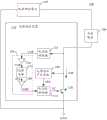
请参照图1。图1显示本发明的一个实施例中,一种电源系统100的方块图。电源系统100被配置为对受电装置190进行供电。电源系统100包含:电源供应单元105以及具有功率限制机制的电源供应装置110。Please refer to Figure 1. FIG. 1 shows a block diagram of a
电源供应单元(Power Supply Unit;PSU)105是用于提供例如,但不限于57伏特或48伏特的电源装置。电源供应装置110包含:开关晶体管120、电压检测电路125、功率限制电路130、电流限制电路135以及反馈电压产生电路140。A power supply unit (Power Supply Unit; PSU) 105 is used to provide a power supply such as, but not limited to, 57V or 48V. The power supply device 110 includes: a
电源供应单元105与受电装置190电性耦接,用以提供电源至受电装置190。开关晶体管120与受电装置190串联,并受控于控制电压VC,以在导通时形成通路,而使电源供应单元105提供电源对受电装置190供电。The
在一个实施例中,电源系统100与受电装置190之间根据以太网供电技术进行电源的传输。因此,在进行电源传输的时候,电源供应装置110工作为供电端设备(PowerSourcing Equipment;PSE),而受电装置190工作为受电端设备(Powered Device;PD)。In one embodiment, power is transmitted between the
在一个实施例中,开关晶体管120是N型晶体管,具有漏极、源极以及栅极。漏极电性耦接于受电装置190,源极电性耦接于接地端GND,栅极接收控制电压VC。开关晶体管120在导通时具有工作电流IOP、工作电压VOP(亦即漏极与源极间的跨压)以及工作功率(未示于图中)。In one embodiment, the
电压检测电路125被配置为检测工作电压VOP。需注意的是,在图1中,电压检测电路125描绘为仅电性耦接于开关晶体管120的漏极,然而为了检测开关晶体管120在漏极与源极间的跨压,电压检测电路125实际上可电性耦接于开关晶体管120的漏极与源极。The
功率限制电路130包含:模拟至数字转换电路150、运算电路155以及数字至模拟转换电路160。The
模拟至数字转换电路150被配置为对工作电压VOP进行模拟至数字转换。The analog-to-
运算电路155被配置为根据经过模拟至数字转换后的工作电压VOP,依照预设电压与电流曲线产生与电流限制值相关的电流限制信号ILS。其中,预设电压与电流曲线使工作电压与电流限制值成反比,进而使开关晶体管120的工作功率不大于预设值。The arithmetic circuit 155 is configured to generate a current limit signal ILS related to a current limit value according to a preset voltage-current curve according to the analog-to-digital converted operating voltage VOP. Wherein, the preset voltage and current curve makes the working voltage and the current limit value inversely proportional, so that the working power of the
请一并参照图2A。图2A显示本发明的一个实施例中,预设电压与电流曲线200的示意图。其中,x轴(水平轴)对应于电压值,y轴(垂直轴)对应于电流值。Please also refer to FIG. 2A . FIG. 2A shows a schematic diagram of a preset voltage and
在本实施例中,预设电压与电流曲线200为直线,并可表示为Y=aX+b,其中X及Y为正数,a为预设负值系数且b为预设正值系数。在一个实际数值示例中,预设电压与电流曲线200可为Y=-X+5。In this embodiment, the preset voltage and
在这样的情况下,由于功率为电压值与电流值的乘积,可表示为X(aX+b),且此功率的二次曲线具有最大值。因此,运算电路155可根据工作电压VOP依照预设电压与电流曲线200计算所需的电流限制值,产生与电流限制值相关的电流限制信号ILS,并确保开关晶体管120的工作功率不大于此曲线的最大值。In such a case, since the power is the product of the voltage value and the current value, it can be expressed as X(aX+b), and the quadratic curve of this power has a maximum value. Therefore, the arithmetic circuit 155 can calculate the required current limit value according to the preset voltage and
请一并参照图2B。图2B显示本发明的一个实施例中,预设电压与电流曲线210的示意图。其中,x轴(水平轴)对应于电压值,y轴(垂直轴)对应于电流值。Please also refer to FIG. 2B. FIG. 2B shows a schematic diagram of a preset voltage and current curve 210 in one embodiment of the present invention. Wherein, the x-axis (horizontal axis) corresponds to the voltage value, and the y-axis (vertical axis) corresponds to the current value.
在本实施例中,预设电压与电流曲线210为反比曲线,并可表示为XY=c,其中X及Y为正数,c为预设正值系数。在一个实际数值示例中,预设电压与电流曲线210可为XY=10。In this embodiment, the preset voltage and current curve 210 is an inverse curve, and can be expressed as XY=c, where X and Y are positive numbers, and c is a preset positive coefficient. In an actual numerical example, the preset voltage and current curve 210 may be XY=10.
在这样的情况下,由于功率为电压值与电流值的乘积,即为c。因此,运算电路155可根据工作电压VOP依照预设电压与电流曲线210计算所需的电流限制值,产生与电流限制值相关的电流限制信号ILS,并确保开关晶体管120的工作功率为不大于c。In such a case, since the power is the product of the voltage value and the current value, it is c. Therefore, the arithmetic circuit 155 can calculate the required current limit value according to the preset voltage and current curve 210 according to the operating voltage VOP, generate a current limit signal ILS related to the current limit value, and ensure that the operating power of the switching
需注意的是,上述的预设电压与电流曲线仅为示例。在其他实施例中,也可能通过其他的曲线达到使工作功率不大于预设值的目的。It should be noted that the above preset voltage and current curves are just examples. In other embodiments, it is also possible to use other curves to achieve the purpose of keeping the working power not greater than the preset value.
数字至模拟转换电路160被配置为对电流限制信号ILS进行数字至模拟转换,以产生参考电压VRF。The digital-to-analog conversion circuit 160 is configured to perform digital-to-analog conversion on the current limit signal ILS to generate a reference voltage VRF.
电流限制电路135被配置为接收参考电压VRF以及根据工作电流IOP反馈产生的反馈电压VFE进行比较并据以产生控制电压VC控制开关晶体管120,以将工作电流IOP维持在电流限制值。其中,反馈电压VFE由反馈电压产生电路140所产生。The current limiting
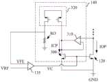
请参照图3。图3显示本发明的一个实施例中,开关晶体管120、电流限制电路135以及反馈电压产生电路140的电路图。其中,反馈电压产生电路140包含:控制晶体管300、比较器310以及电流镜320。Please refer to Figure 3. FIG. 3 shows a circuit diagram of the switching
在一个实施例中,控制晶体管300是N型晶体管,具有漏极、源极以及栅极。漏极电性耦接于比较器310以及电流镜320,源极电性耦接于开关晶体管120的源极,栅极接收控制电压VC。开关晶体管120在导通时具有控制电流ICP。In one embodiment, the
比较器310具有两个输入端以及输出端,两个输入端分别电性耦接于开关晶体管120的漏极以及控制晶体管300的漏极,输出端电性耦接于控制晶体管300的漏极。通过反馈机制比较开关晶体管120以及控制晶体管300的漏极电压使两者的漏极电压相等,比较器310可使控制电流ICP与工作电流IOP呈现固定比例,且此固定比例与开关晶体管120以及控制晶体管300间的通道尺寸(例如宽长比)相关。在一个实施例中,当开关晶体管120以及控制晶体管300的通道尺寸相同时,控制电流ICP与工作电流IOP相同。The
电流镜320具有第一电流输出端以及第二电流输出端,分别电性耦接于控制晶体管300的漏极以及输出电阻RO,以镜射控制电流ICP至输出电阻RO并在第二电流输出端产生反馈电压VFE。The
在一个实施例中,电流限制电路135可以是比较器,被配置为接收反馈电压VFE以及参考电压VRF进行比较,以根据比较结果输出控制电压VC至各个开关晶体管120以及控制晶体管300的栅极。In one embodiment, the current limiting
通过这样的反馈机制,电流限制电路135可在工作电流IOP大于或小于电流限制值时,根据接收反馈电压VFE以及参考电压VRF的比较结果调整控制电压VC的大小,改变开关晶体管120的导通程度,进而将工作电流IOP维持在电流限制值,使开关晶体管120的工作功率不大于预设值。Through such a feedback mechanism, the current limiting
需注意的是,上述反馈电压产生电路140的架构仅为示例。在其他实施例中,也可采用其他的架构达到根据工作电流IOP产生反馈电压VFE的目的。It should be noted that the structure of the feedback
在部分技术中,开关晶体管的功率限制机制利用完全模拟的比较器进行,一方面电压值与电流限制值间的准确性与一致性无法精确的控制,另一方面这样的方式仅能线性调整,在开关晶体管的电流过大进行限流时,为使开关晶体管的导通程度下降,反而会造成开关晶体管的导通电阻上升,进而使功率无法下降。无法弹性的选择适合的曲线来对功率进行控制,将难以实现真正的功率限制。In some technologies, the power limiting mechanism of the switching transistor is implemented by a fully analog comparator. On the one hand, the accuracy and consistency between the voltage value and the current limit value cannot be precisely controlled. On the other hand, this method can only be adjusted linearly. When the current of the switching transistor is too large to limit the current, in order to reduce the conduction degree of the switching transistor, the on-resistance of the switching transistor will increase instead, so that the power cannot be reduced. It will be difficult to achieve true power limitation if you cannot flexibly select a suitable curve to control the power.
本发明的电源供应装置可通过数字的控制,根据转换为数字形式的工作电压依照预设电压与电流曲线,例如使电流与电压成反比的曲线产生电流限制信号,再将电流限制信号转换为模拟形式据以控制开关晶体管的导通状态以使其工作电流维持于电流限制值,达到精确的功率限制机制。The power supply device of the present invention can be digitally controlled, according to the working voltage converted into digital form according to the preset voltage and current curve, for example, the current and voltage are inversely proportional to the curve to generate a current limit signal, and then convert the current limit signal into an analog According to the form, the conduction state of the switching transistor is controlled so that its operating current is maintained at the current limit value to achieve an accurate power limit mechanism.
在一个实施例中,上述图1中的模拟至数字转换电路150以及数字至模拟转换电路160可选择性地与其他可搭配开关晶体管120工作的电路共用。举例而言,模拟至数字转换电路150可与被配置为暂存工作电压VOP的暂存电路(未示于图中)共用,且此暂存电路可为其他电路存取以根据工作电压VOP进行其他运算与处理。数字至模拟转换电路160可与过电流保护(over current protection;OCP)电路(未示于图中)共用。通过这样的配置,电源供应装置110将可对电路面积进行更为有效的利用。In one embodiment, the above-mentioned analog-to-
请参照图4。图4显示本发明一个实施例中,一种电源供应方法400的流程图。Please refer to Figure 4. FIG. 4 shows a flowchart of a
除前述装置外,本发明还公开一种电源供应方法400,应用于例如,但不限于图1的电源供应装置110中。电源供应方法400的一个实施例如图4所示,包含下列步骤。In addition to the aforementioned devices, the present invention also discloses a
在步骤S410,使电源供应装置110中与受电装置190相串联的开关晶体管120受控于控制电压,以在导通时形成通路而使电源供应单元105提供电源对受电装置190供电,开关晶体管120在导通时具有工作电流IOP、工作电压VOP以及工作功率。In step S410, the switching
在步骤S420,使电压检测电路125检测工作电压VOP。In step S420, the
在步骤S430,使功率限制电路130的模拟至数字转换电路150对工作电压VOP进行模拟至数字转换。In step S430 , the analog-to-
在步骤S440,使功率限制电路130的运算电路155根据工作电压VOP依照预设电压与电流曲线产生与电流限制值相关的电流限制信号ILS,其中预设电压与电流曲线使工作功率不大于预设值。In step S440, make the operation circuit 155 of the
在步骤S450,使功率限制电路130的数字至模拟转换电路160对电流限制信号ILS进行数字至模拟转换,以产生参考电压VRF。In step S450 , the digital-to-analog conversion circuit 160 of the
在步骤S460,使电流限制电路135接收参考电压VRF以及根据工作电流IOP反馈产生的反馈电压VFE进行比较并据以产生控制电压VC控制开关晶体管120,以将工作电流IOP维持在电流限制值。In step S460 , the current limiting
需注意的是,上述的实施方式仅为示例。在其他实施例中,本领域普通技术人员可在不违背本发明的精神下进行更改。It should be noted that the above-mentioned embodiments are merely examples. In other embodiments, those skilled in the art can make changes without departing from the spirit of the present invention.
综合上述,本发明中具有功率限制机制的电源供应装置及方法可通过数字的控制,根据转换为数字形式的工作电压依照预设电压与电流曲线产生电流限制信号,再将电流限制信号转换为模拟形式据以控制开关晶体管的导通状态以使其工作电流维持于电流限制值,达到精确的功率限制机制。To sum up the above, the power supply device and method with a power limiting mechanism in the present invention can generate a current limiting signal according to the preset voltage and current curve according to the working voltage converted into a digital form through digital control, and then convert the current limiting signal into an analog According to the form, the conduction state of the switching transistor is controlled so that its operating current is maintained at the current limit value to achieve an accurate power limit mechanism.
虽然本发明的实施例如上所述,然而这些实施例并非用来限定本发明,本领域普通技术人员可依据本发明的明示或隐含的内容对本发明的技术特征施以变化,凡此种种变化均可能属于本发明所寻求的专利保护范围,换言之,本发明的专利保护范围须视本说明书的权利要求所界定的为准。Although the embodiments of the present invention are as described above, these embodiments are not intended to limit the present invention, and those skilled in the art can make changes to the technical characteristics of the present invention according to the explicit or implicit contents of the present invention. All may belong to the scope of patent protection sought by the present invention. In other words, the scope of patent protection of the present invention shall be defined by the claims of this specification.
附图标记说明:Explanation of reference signs:
100:电源系统100: Power system
105:电源供应单元105: Power supply unit
110:电源供应装置110: Power supply device
120:开关晶体管120: switching transistor
125:电压检测电路125: voltage detection circuit
130:功率限制电路130: Power limiting circuit
135:电流限制电路135: current limiting circuit
140:反馈电压产生电路140: Feedback voltage generating circuit
150:模拟至数字转换电路150: Analog to digital conversion circuit
155:运算电路155: Operation circuit
160:数字至模拟转换电路160: Digital to analog conversion circuit
190:受电装置190: Power receiving device
200、210:预设电压与电流曲线200, 210: preset voltage and current curve
300:控制晶体管300: control transistor
310:比较器310: Comparator
320:电流镜320: current mirror
400:电源供应方法400: Power Supply Method
S410~S460:步骤S410~S460: Steps
GND:接地端GND: ground terminal
ICP:控制电流ICP: control current
ILS:电流限制信号ILS: current limit signal
IOP:工作电流IOP: operating current
RO:输出电阻RO: output resistance
VC:控制电压VC: control voltage
VFE:反馈电压VFE: feedback voltage
VOP:工作电压VOP: operating voltage
VRF:参考电压VRF: reference voltage
Claims (10)
Priority Applications (3)
| Application Number | Priority Date | Filing Date | Title |
|---|---|---|---|
| CN202111285556.6ACN116073658A (en) | 2021-11-02 | 2021-11-02 | Power supply device and method with power limiting mechanism |
| TW111100977ATWI801088B (en) | 2021-11-02 | 2022-01-10 | Power supply apparatus and method having power limitation mechanism |
| US17/844,779US11860709B2 (en) | 2021-11-02 | 2022-06-21 | Power supply apparatus and method having power limiting mechanism |
Applications Claiming Priority (1)
| Application Number | Priority Date | Filing Date | Title |
|---|---|---|---|
| CN202111285556.6ACN116073658A (en) | 2021-11-02 | 2021-11-02 | Power supply device and method with power limiting mechanism |
Publications (1)
| Publication Number | Publication Date |
|---|---|
| CN116073658Atrue CN116073658A (en) | 2023-05-05 |
Family
ID=86146198
Family Applications (1)
| Application Number | Title | Priority Date | Filing Date |
|---|---|---|---|
| CN202111285556.6APendingCN116073658A (en) | 2021-11-02 | 2021-11-02 | Power supply device and method with power limiting mechanism |
Country Status (3)
| Country | Link |
|---|---|
| US (1) | US11860709B2 (en) |
| CN (1) | CN116073658A (en) |
| TW (1) | TWI801088B (en) |
Cited By (1)
| Publication number | Priority date | Publication date | Assignee | Title |
|---|---|---|---|---|
| CN117424767B (en)* | 2023-12-18 | 2024-02-23 | 晶艺半导体有限公司 | Communication handshake circuit and method applied to POE system |
Families Citing this family (1)
| Publication number | Priority date | Publication date | Assignee | Title |
|---|---|---|---|---|
| CN119966386A (en)* | 2024-11-29 | 2025-05-09 | 无锡市稳先微电子有限公司 | Intelligent electronic switches, chips, chip products and electromechanical devices that reduce power |
Citations (4)
| Publication number | Priority date | Publication date | Assignee | Title |
|---|---|---|---|---|
| CN101667772A (en)* | 2008-09-04 | 2010-03-10 | 绿达光电股份有限公司 | Digital overcurrent protection device for power supply and related power supply |
| KR20120129209A (en)* | 2011-05-19 | 2012-11-28 | (주)태진기술 | Current Limit circuit |
| CN105811759A (en)* | 2014-12-29 | 2016-07-27 | 登丰微电子股份有限公司 | Power supply device |
| US20180006643A1 (en)* | 2016-06-29 | 2018-01-04 | Texas Instruments Incorporated | Methods and Apparatus for Continuous Current Limiting for FETS in High Inductive Load Systems |
Family Cites Families (13)
| Publication number | Priority date | Publication date | Assignee | Title |
|---|---|---|---|---|
| US7567579B2 (en)* | 1999-08-02 | 2009-07-28 | Microsemi Corp.-Analog Mixed Signal Group Ltd. | Multiple current limits for power over ethernet controller |
| US7554783B2 (en)* | 2005-01-25 | 2009-06-30 | Linear Technology Corporation | High-power foldback mechanism in system for providing power over communication link |
| US7639469B2 (en)* | 2005-01-25 | 2009-12-29 | Linear Technology Corporation | Power sourcing equipment having auto-zero circuit for determining and controlling output current |
| US9769090B2 (en)* | 2005-01-25 | 2017-09-19 | Linear Technology Corporation | Adjusting current limit thresholds based on power requirement of powered device in system for providing power over communication link |
| CN101124771A (en)* | 2005-01-25 | 2008-02-13 | 凌特公司 | Power supply equipment with an auto-zeroing circuit for determining and controlling the output current |
| US7839154B2 (en)* | 2007-01-05 | 2010-11-23 | Broadcom Corporation | Powered device power classification with increased current limit |
| US9927779B2 (en)* | 2012-11-19 | 2018-03-27 | Silicon Laboratories Inc. | Power sourcing equipment and method of detecting inrush fault errors |
| TWI675278B (en)* | 2015-11-09 | 2019-10-21 | 力智電子股份有限公司 | Parameter setting circuit of a power conversion apparatus and a method for generating a currcnt |
| CN108627699A (en)* | 2017-03-24 | 2018-10-09 | 瑞昱半导体股份有限公司 | detection device and detection method |
| US10845396B2 (en)* | 2018-09-19 | 2020-11-24 | Texas Instruments Incorporated | Apparatus and system for wide-range current sensing |
| US10609797B1 (en)* | 2019-05-06 | 2020-03-31 | Karl S Jonsson | Constant current dimming of constant voltage loads |
| US11506695B2 (en)* | 2020-04-13 | 2022-11-22 | Skyworks Solutions, Inc. | Calibration of the external resistance value in the power sourcing equipment of a POE system |
| CN113572622B (en)* | 2021-07-08 | 2023-10-31 | 浙江大华技术股份有限公司 | POE power supply system and POE power supply method |
- 2021
- 2021-11-02CNCN202111285556.6Apatent/CN116073658A/enactivePending
- 2022
- 2022-01-10TWTW111100977Apatent/TWI801088B/enactive
- 2022-06-21USUS17/844,779patent/US11860709B2/enactiveActive
Patent Citations (4)
| Publication number | Priority date | Publication date | Assignee | Title |
|---|---|---|---|---|
| CN101667772A (en)* | 2008-09-04 | 2010-03-10 | 绿达光电股份有限公司 | Digital overcurrent protection device for power supply and related power supply |
| KR20120129209A (en)* | 2011-05-19 | 2012-11-28 | (주)태진기술 | Current Limit circuit |
| CN105811759A (en)* | 2014-12-29 | 2016-07-27 | 登丰微电子股份有限公司 | Power supply device |
| US20180006643A1 (en)* | 2016-06-29 | 2018-01-04 | Texas Instruments Incorporated | Methods and Apparatus for Continuous Current Limiting for FETS in High Inductive Load Systems |
Cited By (1)
| Publication number | Priority date | Publication date | Assignee | Title |
|---|---|---|---|---|
| CN117424767B (en)* | 2023-12-18 | 2024-02-23 | 晶艺半导体有限公司 | Communication handshake circuit and method applied to POE system |
Also Published As
| Publication number | Publication date |
|---|---|
| TW202320513A (en) | 2023-05-16 |
| US20230132775A1 (en) | 2023-05-04 |
| US11860709B2 (en) | 2024-01-02 |
| TWI801088B (en) | 2023-05-01 |
Similar Documents
| Publication | Publication Date | Title |
|---|---|---|
| US10411504B2 (en) | System and method for controlling power delivered to a powered device through a communication cable | |
| CN116073658A (en) | Power supply device and method with power limiting mechanism | |
| EP2712086B1 (en) | Drive device for driving voltage-driven element | |
| US8386088B2 (en) | Powered device including a multi-use detection resistor | |
| CN110166259B (en) | Monitoring circuit for supporting power over Ethernet receiving end equipment | |
| EP2060059B1 (en) | Programmable constant power foldback | |
| JP2005333691A (en) | Overcurrent detection circuit and power supply having it | |
| CN114069553B (en) | Overvoltage protection circuit | |
| JP2021502049A (en) | High voltage gate driver current source | |
| CN111366788A (en) | Chip resistance detection device and chip device | |
| US20200387186A1 (en) | Reference voltage generating circuit | |
| CN107800540B (en) | Power supply device, detection circuit and power supply method thereof | |
| JP2022540957A (en) | Method and apparatus for current sensing and current limiting | |
| US11171645B1 (en) | Transistor switching circuit and integrated circuit thereof | |
| CN103199488A (en) | Low-voltage protection circuit free of requiring independent reference source | |
| CN1381774A (en) | Voltage control circuit | |
| CN113726329A (en) | Self-adaptive single-ended and differential signal input interface circuit | |
| KR20100034312A (en) | Remote sensing circuit in high power supply apparatus, and high power supply apparatus having it | |
| CN111756029A (en) | High-speed wide dynamic range input structure | |
| US11719728B2 (en) | Apparatus and system for wide-range current sensing | |
| CN107492929B (en) | Charging circuit provided with current protection circuit | |
| CN115754441A (en) | Overcurrent detection circuit, overcurrent detection method, overcurrent protection circuit and chip | |
| CN103245904A (en) | Method and device for testing functional circuit | |
| CN108919875B (en) | Enable generating circuit and its enabling control method | |
| CN110031671B (en) | Drive overcurrent detection circuit |
Legal Events
| Date | Code | Title | Description |
|---|---|---|---|
| PB01 | Publication | ||
| PB01 | Publication | ||
| SE01 | Entry into force of request for substantive examination | ||
| SE01 | Entry into force of request for substantive examination |