CN116073156A - Connectors for high-speed transmission - Google Patents
Connectors for high-speed transmissionDownload PDFInfo
- Publication number
- CN116073156A CN116073156ACN202111289444.8ACN202111289444ACN116073156ACN 116073156 ACN116073156 ACN 116073156ACN 202111289444 ACN202111289444 ACN 202111289444ACN 116073156 ACN116073156 ACN 116073156A
- Authority
- CN
- China
- Prior art keywords
- contact
- contacts
- metal member
- bent
- grounding
- Prior art date
- Legal status (The legal status is an assumption and is not a legal conclusion. Google has not performed a legal analysis and makes no representation as to the accuracy of the status listed.)
- Pending
Links
Images


Classifications
- H—ELECTRICITY
- H01—ELECTRIC ELEMENTS
- H01R—ELECTRICALLY-CONDUCTIVE CONNECTIONS; STRUCTURAL ASSOCIATIONS OF A PLURALITY OF MUTUALLY-INSULATED ELECTRICAL CONNECTING ELEMENTS; COUPLING DEVICES; CURRENT COLLECTORS
- H01R13/00—Details of coupling devices of the kinds covered by groups H01R12/70 or H01R24/00 - H01R33/00
- H01R13/02—Contact members
- H—ELECTRICITY
- H01—ELECTRIC ELEMENTS
- H01R—ELECTRICALLY-CONDUCTIVE CONNECTIONS; STRUCTURAL ASSOCIATIONS OF A PLURALITY OF MUTUALLY-INSULATED ELECTRICAL CONNECTING ELEMENTS; COUPLING DEVICES; CURRENT COLLECTORS
- H01R12/00—Structural associations of a plurality of mutually-insulated electrical connecting elements, specially adapted for printed circuits, e.g. printed circuit boards [PCB], flat or ribbon cables, or like generally planar structures, e.g. terminal strips, terminal blocks; Coupling devices specially adapted for printed circuits, flat or ribbon cables, or like generally planar structures; Terminals specially adapted for contact with, or insertion into, printed circuits, flat or ribbon cables, or like generally planar structures
- H01R12/70—Coupling devices
- H01R12/71—Coupling devices for rigid printing circuits or like structures
- H01R12/72—Coupling devices for rigid printing circuits or like structures coupling with the edge of the rigid printed circuits or like structures
- H01R12/722—Coupling devices for rigid printing circuits or like structures coupling with the edge of the rigid printed circuits or like structures coupling devices mounted on the edge of the printed circuits
- H01R12/724—Coupling devices for rigid printing circuits or like structures coupling with the edge of the rigid printed circuits or like structures coupling devices mounted on the edge of the printed circuits containing contact members forming a right angle
- H—ELECTRICITY
- H01—ELECTRIC ELEMENTS
- H01R—ELECTRICALLY-CONDUCTIVE CONNECTIONS; STRUCTURAL ASSOCIATIONS OF A PLURALITY OF MUTUALLY-INSULATED ELECTRICAL CONNECTING ELEMENTS; COUPLING DEVICES; CURRENT COLLECTORS
- H01R12/00—Structural associations of a plurality of mutually-insulated electrical connecting elements, specially adapted for printed circuits, e.g. printed circuit boards [PCB], flat or ribbon cables, or like generally planar structures, e.g. terminal strips, terminal blocks; Coupling devices specially adapted for printed circuits, flat or ribbon cables, or like generally planar structures; Terminals specially adapted for contact with, or insertion into, printed circuits, flat or ribbon cables, or like generally planar structures
- H01R12/50—Fixed connections
- H01R12/51—Fixed connections for rigid printed circuits or like structures
- H01R12/52—Fixed connections for rigid printed circuits or like structures connecting to other rigid printed circuits or like structures
- H—ELECTRICITY
- H01—ELECTRIC ELEMENTS
- H01R—ELECTRICALLY-CONDUCTIVE CONNECTIONS; STRUCTURAL ASSOCIATIONS OF A PLURALITY OF MUTUALLY-INSULATED ELECTRICAL CONNECTING ELEMENTS; COUPLING DEVICES; CURRENT COLLECTORS
- H01R12/00—Structural associations of a plurality of mutually-insulated electrical connecting elements, specially adapted for printed circuits, e.g. printed circuit boards [PCB], flat or ribbon cables, or like generally planar structures, e.g. terminal strips, terminal blocks; Coupling devices specially adapted for printed circuits, flat or ribbon cables, or like generally planar structures; Terminals specially adapted for contact with, or insertion into, printed circuits, flat or ribbon cables, or like generally planar structures
- H01R12/50—Fixed connections
- H01R12/51—Fixed connections for rigid printed circuits or like structures
- H01R12/55—Fixed connections for rigid printed circuits or like structures characterised by the terminals
- H01R12/57—Fixed connections for rigid printed circuits or like structures characterised by the terminals surface mounting terminals
- H—ELECTRICITY
- H01—ELECTRIC ELEMENTS
- H01R—ELECTRICALLY-CONDUCTIVE CONNECTIONS; STRUCTURAL ASSOCIATIONS OF A PLURALITY OF MUTUALLY-INSULATED ELECTRICAL CONNECTING ELEMENTS; COUPLING DEVICES; CURRENT COLLECTORS
- H01R12/00—Structural associations of a plurality of mutually-insulated electrical connecting elements, specially adapted for printed circuits, e.g. printed circuit boards [PCB], flat or ribbon cables, or like generally planar structures, e.g. terminal strips, terminal blocks; Coupling devices specially adapted for printed circuits, flat or ribbon cables, or like generally planar structures; Terminals specially adapted for contact with, or insertion into, printed circuits, flat or ribbon cables, or like generally planar structures
- H01R12/70—Coupling devices
- H01R12/71—Coupling devices for rigid printing circuits or like structures
- H01R12/72—Coupling devices for rigid printing circuits or like structures coupling with the edge of the rigid printed circuits or like structures
- H01R12/722—Coupling devices for rigid printing circuits or like structures coupling with the edge of the rigid printed circuits or like structures coupling devices mounted on the edge of the printed circuits
- H01R12/727—Coupling devices presenting arrays of contacts
- H—ELECTRICITY
- H01—ELECTRIC ELEMENTS
- H01R—ELECTRICALLY-CONDUCTIVE CONNECTIONS; STRUCTURAL ASSOCIATIONS OF A PLURALITY OF MUTUALLY-INSULATED ELECTRICAL CONNECTING ELEMENTS; COUPLING DEVICES; CURRENT COLLECTORS
- H01R13/00—Details of coupling devices of the kinds covered by groups H01R12/70 or H01R24/00 - H01R33/00
- H01R13/40—Securing contact members in or to a base or case; Insulating of contact members
- H—ELECTRICITY
- H01—ELECTRIC ELEMENTS
- H01R—ELECTRICALLY-CONDUCTIVE CONNECTIONS; STRUCTURAL ASSOCIATIONS OF A PLURALITY OF MUTUALLY-INSULATED ELECTRICAL CONNECTING ELEMENTS; COUPLING DEVICES; CURRENT COLLECTORS
- H01R13/00—Details of coupling devices of the kinds covered by groups H01R12/70 or H01R24/00 - H01R33/00
- H01R13/46—Bases; Cases
- H01R13/514—Bases; Cases composed as a modular blocks or assembly, i.e. composed of co-operating parts provided with contact members or holding contact members between them
- H—ELECTRICITY
- H01—ELECTRIC ELEMENTS
- H01R—ELECTRICALLY-CONDUCTIVE CONNECTIONS; STRUCTURAL ASSOCIATIONS OF A PLURALITY OF MUTUALLY-INSULATED ELECTRICAL CONNECTING ELEMENTS; COUPLING DEVICES; CURRENT COLLECTORS
- H01R13/00—Details of coupling devices of the kinds covered by groups H01R12/70 or H01R24/00 - H01R33/00
- H01R13/646—Details of coupling devices of the kinds covered by groups H01R12/70 or H01R24/00 - H01R33/00 specially adapted for high-frequency, e.g. structures providing an impedance match or phase match
- H01R13/6461—Means for preventing cross-talk
- H—ELECTRICITY
- H01—ELECTRIC ELEMENTS
- H01R—ELECTRICALLY-CONDUCTIVE CONNECTIONS; STRUCTURAL ASSOCIATIONS OF A PLURALITY OF MUTUALLY-INSULATED ELECTRICAL CONNECTING ELEMENTS; COUPLING DEVICES; CURRENT COLLECTORS
- H01R13/00—Details of coupling devices of the kinds covered by groups H01R12/70 or H01R24/00 - H01R33/00
- H01R13/648—Protective earth or shield arrangements on coupling devices, e.g. anti-static shielding
- H01R13/658—High frequency shielding arrangements, e.g. against EMI [Electro-Magnetic Interference] or EMP [Electro-Magnetic Pulse]
- H01R13/6581—Shield structure
- H01R13/6585—Shielding material individually surrounding or interposed between mutually spaced contacts
- H—ELECTRICITY
- H01—ELECTRIC ELEMENTS
- H01R—ELECTRICALLY-CONDUCTIVE CONNECTIONS; STRUCTURAL ASSOCIATIONS OF A PLURALITY OF MUTUALLY-INSULATED ELECTRICAL CONNECTING ELEMENTS; COUPLING DEVICES; CURRENT COLLECTORS
- H01R43/00—Apparatus or processes specially adapted for manufacturing, assembling, maintaining, or repairing of line connectors or current collectors or for joining electric conductors
- H01R43/16—Apparatus or processes specially adapted for manufacturing, assembling, maintaining, or repairing of line connectors or current collectors or for joining electric conductors for manufacturing contact members, e.g. by punching and by bending
- H—ELECTRICITY
- H01—ELECTRIC ELEMENTS
- H01R—ELECTRICALLY-CONDUCTIVE CONNECTIONS; STRUCTURAL ASSOCIATIONS OF A PLURALITY OF MUTUALLY-INSULATED ELECTRICAL CONNECTING ELEMENTS; COUPLING DEVICES; CURRENT COLLECTORS
- H01R13/00—Details of coupling devices of the kinds covered by groups H01R12/70 or H01R24/00 - H01R33/00
- H01R13/646—Details of coupling devices of the kinds covered by groups H01R12/70 or H01R24/00 - H01R33/00 specially adapted for high-frequency, e.g. structures providing an impedance match or phase match
- H01R13/6461—Means for preventing cross-talk
- H01R13/6471—Means for preventing cross-talk by special arrangement of ground and signal conductors, e.g. GSGS [Ground-Signal-Ground-Signal]
Landscapes
- Engineering & Computer Science (AREA)
- Manufacturing & Machinery (AREA)
- Details Of Connecting Devices For Male And Female Coupling (AREA)
Abstract
Description
Translated fromChinese技术领域technical field
本发明涉及高速传输用连接器。The present invention relates to a connector for high-speed transmission.
背景技术Background technique
已提出有各种关于降低高速传输用连接器的串扰的技术。例如,专利文献1中记载的连接器组件通过桥(bridge)来连接外壳内夹着高速信号端子而配置的多个接地端子,从而减少桥两侧的接地端子的电长度,以避免串扰的发生。Various techniques for reducing crosstalk in connectors for high-speed transmission have been proposed. For example, the connector assembly described in
现有技术文献prior art literature
专利文献patent documents
专利文献1:日本特许第5405582号说明书。Patent Document 1: Specification of Japanese Patent No. 5405582.
发明内容Contents of the invention
发明要解决的课题The problem to be solved by the invention
然而,专利文献1的连接器组件的桥成为以从侧方包裹两个接地端子的方式固定的构造,期望有能够通过更加简单的结构来实现降低串扰的技术手段。However, the bridge of the connector assembly of
本发明鉴于这样的课题而构思,其主要目的之一就是提供一种能够降低串扰的高速传输用连接器。The present invention is conceived in view of such problems, and one of its main purposes is to provide a high-speed transmission connector capable of reducing crosstalk.
用于解决课题的方案Solution to the problem
为了解决上述课题,作为本发明的优选方式的高速传输用连接器具备:外壳,具有使通信对象嵌合的开口部;多个接触件的列,包含接地用的接触件;以及金属部件,配置在所述接触件的列,使所述接地用的接触件短路,以避开所述接地用的接触件以外的接触件的方式弯曲,所述接触件具有:与所述通信对象接触的接触部、从所述接触部的后端向后方延伸的第1直线部、从所述第1直线部的后端弯曲并延伸的第2直线部、和在所述第2直线部的前端焊接到外部的基板的端子部,所述金属部件配置成在所述多个接触件的列的一端的接触件与另一端的接触件之间延伸,具有横跨所述接地用的接触件以外的接触件而以U字状弯曲的弯曲部,并与所述接地用的接触件的所述第1直线部及所述第2直线部的至少一个连接。In order to solve the above-mentioned problems, a high-speed transmission connector as a preferred embodiment of the present invention includes: a housing having an opening for fitting a communication partner; a row of a plurality of contacts including contacts for grounding; and a metal member arranged In the row of the contacts, the grounding contacts are short-circuited and bent so as to avoid contacts other than the grounding contacts, and the contacts have a contact with the communication partner. part, the first straight part extending backward from the rear end of the contact part, the second straight part bent and extending from the rear end of the first straight part, and the front end of the second straight part welded to In the terminal portion of the outer substrate, the metal member is arranged to extend between the contact at one end and the contact at the other end of the row of the plurality of contacts, and has a contact other than the contact for grounding. The bent portion bent in a U-shape is connected to at least one of the first straight portion and the second straight portion of the ground contact.
发明效果Invention effect
依据本发明的一种方式的高速传输用连接器,具备配置在被外壳支撑的接触件的上侧及下侧的至少任一侧并使接地用的接触件短路而以避开接地用的接触件以外的接触件的方式弯曲的金属部件,所述接触件具有:与所述通信对象接触的接触部、从所述接触部的后端向后方延伸的第1直线部、从所述第1直线部的后端弯曲并延伸的第2直线部、和在所述第2直线部的前端焊接到外部的基板的端子部,所述金属部件配置成在所述多个接触件的列的一端的接触件与另一端的接触件之间延伸,具有横跨所述接地用以外的接触件而以U字状弯曲的弯曲部,并与所述接地用的接触件的所述第1直线部及所述第2直线部的至少一个连接,因此提供以简单的结构降低串扰的连接器。According to one aspect of the present invention, a high-speed transmission connector includes a connector that is arranged on at least one of the upper side and the lower side of the contacts supported by the housing and short-circuits the grounding contacts to avoid the grounding contacts. A metal part bent in the form of a contact piece other than a contact piece, the contact piece has: a contact portion that contacts the communication partner, a first straight line portion extending backward from the rear end of the contact portion, and a straight line portion extending from the first a second straight portion whose rear end is bent and extended, and a terminal portion welded to an external substrate at a front end of the second straight portion, the metal member being arranged at one end of the row of the plurality of contacts extending between the contact piece and the contact piece at the other end, has a U-shaped bent portion straddling the contact piece other than the grounding piece, and is connected to the first straight line portion of the grounding piece And at least one connection of the second linear portion, thus providing a connector that reduces crosstalk with a simple structure.
附图说明Description of drawings
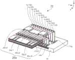
图1是示出依据本发明的第1实施方式的连接器的外观结构的立体图的一个例子。FIG. 1 is an example of a perspective view showing an appearance structure of a connector according to a first embodiment of the present invention.
图2是图1所示的连接器的正视图,并且是示出光收发器头部的上下表面的PIN排列的一个例子的图。FIG. 2 is a front view of the connector shown in FIG. 1 and is a diagram showing an example of a PIN arrangement on the upper and lower surfaces of the optical transceiver head.
图3是从图1所示的连接器省略外壳而明确了接触件及上侧金属部件的概略结构的立体图的一个例子。3 is an example of a perspective view illustrating a schematic structure of a contact and an upper metal member by omitting a housing from the connector shown in FIG. 1 .
图4是图3所示的概略结构的右侧视图。Fig. 4 is a right side view of the schematic structure shown in Fig. 3 .
图5是图3所示的上侧金属部件的放大图的一个例子。Fig. 5 is an example of an enlarged view of the upper metal member shown in Fig. 3 .
图6是示出图4所示的下侧金属部件的立体图的一个例子。FIG. 6 is an example of a perspective view showing the lower metal member shown in FIG. 4 .
图7是关于第1实施方式的连接器示出金属部件的串扰改善效果有关的模拟结果的一个例子的图表。FIG. 7 is a graph showing an example of simulation results related to the effect of improving crosstalk of metal components with respect to the connector according to the first embodiment.
图8是关于第1实施方式的连接器示出金属部件的串扰改善效果有关的模拟结果的另一个例子的图表。FIG. 8 is a graph showing another example of simulation results related to the crosstalk improvement effect of metal components with respect to the connector according to the first embodiment.
图9是关于第1实施方式的连接器示出金属部件的串扰改善效果有关的模拟结果的又一个例子的图表。FIG. 9 is a graph showing still another example of simulation results related to the crosstalk improvement effect of metal components with respect to the connector according to the first embodiment.
图10是关于上侧金属部件的宽度示出用于求出合适值的串扰的模拟结果的一个例子的图表。FIG. 10 is a graph showing an example of simulation results for obtaining an appropriate value of crosstalk with respect to the width of the upper metal member.
图11是有关于下侧金属部件的宽度示出用于求出合适值的串扰的模拟结果的一个例子的图表。FIG. 11 is a graph showing an example of simulation results for obtaining an appropriate value of crosstalk with respect to the width of the lower metal member.
图12是在与图4所示的位置不同的位置配置金属部件的一个例子。FIG. 12 shows an example in which metal components are arranged at positions different from those shown in FIG. 4 .
图13是示出用于求出将金属部件配置在图4所示的位置的情况和将金属部件配置在图12所示的位置的情况下的串扰差异的模拟结果的一个例子的图表。FIG. 13 is a graph showing an example of simulation results for obtaining a difference in crosstalk between the case where the metal member is arranged at the position shown in FIG. 4 and the case where the metal member is arranged at the position shown in FIG. 12 .
图14是关于金属部件示出仅连接一部分GND时的结构的一个例子的立体图的一个例子。FIG. 14 is an example of a perspective view showing an example of a structure when only a part of GND is connected to a metal member.
图15是示出用于求出关于图3及图14所示的各个结构例的串扰差异的模拟结果的一个例子的图表。FIG. 15 is a graph showing an example of a simulation result for obtaining a difference in crosstalk with respect to each configuration example shown in FIGS. 3 and 14 .
图16是示出设置了多对金属部件的连接器的一个例子的图。FIG. 16 is a diagram showing an example of a connector provided with a plurality of pairs of metal members.
图17是示出在改变金属部件中各个弯曲部的高度时的阻抗特性的模拟结果的一个例子的图。FIG. 17 is a graph showing an example of a simulation result of impedance characteristics when the height of each bent portion in a metal member is changed.
图18是示出依据本发明的第2实施方式的连接器的PIN排列的一个例子的图。FIG. 18 is a diagram showing an example of a PIN arrangement of the connector according to the second embodiment of the present invention.
图19是从第2实施方式的连接器省略外壳而示出接触件及上侧的金属部件的概略结构的立体图的一个例子。19 is an example of a perspective view showing a schematic configuration of a contact and an upper metal member, omitting the housing from the connector of the second embodiment.
图20是从斜下方观看图19所示的概略结构的立体图的一个例子。FIG. 20 is an example of a perspective view of the schematic structure shown in FIG. 19 viewed obliquely from below.
图21是示出第2实施方式中金属部件的串扰改善效果有关的模拟结果的一个例子的图表。FIG. 21 is a graph showing an example of simulation results related to the crosstalk improvement effect of metal components in the second embodiment.
图22是示出第2实施方式中金属部件的串扰改善效果有关的模拟结果的另一个例子的图表。22 is a graph showing another example of simulation results related to the crosstalk improvement effect of metal components in the second embodiment.
图23是示出第2实施方式中金属部件的串扰改善效果有关的模拟结果的又一个例子的图表。23 is a graph showing still another example of simulation results related to the crosstalk improvement effect of metal components in the second embodiment.
具体实施方式Detailed ways
以下,参照附图,对本发明的一些实施方式进行说明。对于附图中相同或对应的要素/构件标注相同的参照标号,并适当省略其重复说明。另外,需要说明的是,为了便于说明,有时对图中各构件的形状/尺寸进行适当放大/缩小/省略而与实际的比例尺/比例不一致。Hereinafter, some embodiments of the present invention will be described with reference to the drawings. The same or corresponding elements/members in the drawings are marked with the same reference numerals, and repeated explanations thereof are appropriately omitted. In addition, it should be noted that, for convenience of description, the shapes/dimensions of the components in the drawings may be appropriately enlarged/reduced/omitted, and may not match the actual scale/ratio.
以下使用的第1、第2等表示序数的术语只是用于区分相同或相应的构成要素的识别符号,相同或相应的构成要素并不受第1、第2等术语限制。The 1st, 2nd, and other ordinal terms used below are only identification symbols for distinguishing the same or corresponding constituent elements, and the same or corresponding constituent elements are not limited by the 1st, 2nd, etc. terms.
本申请说明书中“连接”或“结合”是不仅仅指在各构成要素间的接触关系上直接在各构成要素间物理接触的情况,而且是还包含其他结构介于各构成要素间,构成要素分别与其他结构接触的情况的概念。另外,术语“实质上”是用于表示还包括测定误差。"Connection" or "combination" in the specification of this application not only refers to the situation of direct physical contact between each constituent element in the contact relationship between each constituent element, but also includes other structures interposed between each constituent element, constituent elements The concept of situations in contact with other structures, respectively. In addition, the term "substantially" is used to mean that measurement errors are also included.
(1)第1实施方式(1) The first embodiment
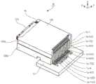
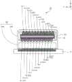
如图1至图4所示,依据第1实施方式的高速传输用连接器6被安装在电路基板S1上而使用。在高速传输用连接器6的插槽40中,会嵌合作为通信对象的装置的光收发器5的头部7。在头部7的前端露出成为电接口的印刷板即卡缘,印刷板的各PIN与连接器6的各接触件通过对插槽40的嵌合而电连接。插槽40例如与权利要求书中规定的“开口部”对应。此外,在图1中为了便于理解而省略了头部7以外的光收发器5的部分。As shown in FIGS. 1 to 4 , the high-
在以下的说明中,将高速传输用连接器6相对于电路基板S1的安装方向称为Z方向,并将光收发器5向高速传输用连接器6的插槽40嵌合的方向称为X方向,与Z方向及X方向这两个方向正交的方向和称为Y方向。另外,将Z方向上高速传输用连接器6一侧即+Z侧适当称为“上侧”,并将电路基板一侧即-Z侧适当称为“下侧”。另外,将X方向上光收发器5一侧即+X侧适当称为“前侧”,并将高速传输用连接器6一侧即-X侧适当称为“后侧”。另外,从光收发器5一侧即+X侧观看,将左侧即+Y侧适当简称为“左侧”,并且从光收发器5一侧即+X侧观看,将右侧即-Y侧适当简称为“右侧”。In the following description, the mounting direction of the high-
虽然没有特别图示,但本实施方式中光收发器5呈棒(stick)状,头部7从其前侧的端部突出。头部7的上侧和左右两侧被壳体覆盖。如图2所示,在头部7的上表面形成有第1~第11焊盘列。Although not particularly shown, in this embodiment, the
例如,如在图7上排的PIN排列表记载的那样,在本实施方式中头部7的上侧的第1~第11PIN的列对应于图7的PIN排列(Top)而配置如下。即,在左端的第1PIN配置有电力线(PWR),从左端起第2个的第2PIN、第4个的第4PIN、第5个的第5PIN、第6个的第6PIN、第7个的第7PIN的列、第9个的第9PIN及右端的第11个的第11PIN的每一个上,被分配了接地用的接触件GND。另外,从左端起第3个的第3PIN及从右端起第2个的第10PIN上,被分别分配了接收信号用接触件RX1、发送信号用接触件TX1。从左端起第8个的第8PIN上,被分配了低速控制信号用接触件LS。For example, as described in the PIN arrangement table in the upper row of FIG. 7 , the first to eleventh PIN columns on the upper side of the
在本实施方式中,头部7的下表面的第1~第11PIN的列与图7的PIN排列(Bottom)对应,配置如下。即,在左端的第1PIN、从左端起第3个的第3PIN、从左端起第5及第6个的第5及第6PIN以及从左端起第8及第10个的第8及第10PIN的每一个上,被分配了接地用接触件GND。另外,从左端起第2个的第2PIN及从右端起第3个的第9PIN上,被分别分配了接收信号用接触件RX2、发送信号用接触件TX2。进而,在从左端起第4个的第4PIN及第7个的第7PIN的每一个上,被分配了低速控制信号用接触件LS。In this embodiment, the columns of the first to eleventh PINs on the lower surface of the
如图1至图3所示,高速传输用连接器6具有:外壳100;接触件1a-k(k=1~11);以及接触件1b-k(k=1~11)。如图4所示,接触件1a-k(k=1~11)及1b-k(k=1~11)分别是使棒状的金属片沿前后延伸且使其在多个部位弯曲的部件,沿左右并排地配置了k(=11)个,分别与图2所示的PIN排列的从左端到右端(从左端第1个到第11个)对应。接触件1a-k(k=1~11)及接触件1b-k(k=1~11)例如与权利要求书中规定的“第1接触件的列”及“第2接触件的列”分别对应。As shown in FIGS. 1 to 3 , the high-
如图2所示,外壳100具有上部外壳100a和下部外壳100b,在本实施方式中,这些外壳100a、100b例如以塑料为材料一体成型。上排的接触件1a-k(k=1~11)被上部外壳100a支撑,下排的接触件1b-k(k=1~11)被下部外壳100b支撑。上部外壳100a及下部外壳100b例如与权利要求书中规定的“上板部”和“下板部”分别对应。As shown in FIG. 2 , the
如图4的示意性右侧视图所示,接触件1a-k具有:弯曲成倒拱形的前端侧接触部11a;从前端侧接触部11a的后端向后侧延伸的直线部12a;从直线部12a的后端向下侧延伸的直线部13a;以及从直线部13a的下端沿后侧延伸的基板侧接触部14a。基板侧接触部14a通过焊接等来电连接到基板S1上的对应的焊盘。As shown in the schematic right side view of FIG. 4, the
应对于接触件1a-k的形状,接触件1b-k具有:弯曲成拱形的前端侧接触部11b;从前端侧接触部11b的后端向接触件1b-k的后侧延伸的直线部12b;从直线部12b的后端向下侧弯曲并延伸到下侧的直线部13b;以及从直线部13b的下端沿前侧弯曲并延伸到前侧的基板侧接触部14b。基板侧接触部14b也通过焊接等来电连接到基板S1上的对应的焊盘。Corresponding to the shape of the
在本实施方式中,前端侧接触部11a、11b例如与权利要求书中规定的“接触部”对应,直线部12a、12b例如与权利要求书中规定的“第1直线部”对应。另外,直线部13a、13b例如与权利要求书中规定的“第2直线部”对应,基板侧接触部14a、14b例如与权利要求书中规定的“端子部”对应。In the present embodiment, the front-end
此外,在附图中,适当地对与接地用接触件GND接触的接触件1a-k、1b-k加上字符(G),并且对与信号用接触件SIG接触的接触件1a-k、1b-k加上字符(S),以区分两者。In addition, in the drawings, the character (G) is appropriately added to the contacts 1ak, 1b-k that are in contact with the ground contact GND, and the
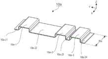
如图3及图4所示,本实施方式的高速传输用连接器6具有金属部件10a,该金属部件10a在接触件1a-k的列上的一端的接触件(例如,1a-1)到另一端的接触件(例如,1a-11)之间沿左右(Y方向)配置在接触件1a-k的上侧。As shown in FIG. 3 and FIG. 4 , the high-
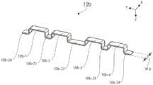
另外,如图4所示,高速传输用连接器6具有金属部件10b,该金属部件10b在接触件1b-k的列上的一端的接触件(例如,1b-1)到另一端的接触件(例如,1b-11)之间沿左右(Y方向)配置在接触件1b-k的下侧。In addition, as shown in FIG. 4, the
作为金属部件10a、10b的材料,可以使用与一般的导体相同的材料,例如铜(Cu)、铜合金、铝(Al)、金(Au)等。As the material of the
金属部件10a具有:图7所示的表的上排(Top)的第1~第11PIN排列之中与跟接地用PIN连接的接地用接触件1a-k电连接的基底部10a-21、10a-22、10a-23、10a-24;以及以避开除这些接地用接触件以外的其他信号用接触件1a-k的方式呈倒置“U”字的形状向上侧弯曲的弯曲部10a-1、10a-2、10a-3。更具体而言,如图3及图5所示,在本实施方式中,金属部件10a具有这样的形状:在基底部与接触件1a-2(G)、1a-4(G)~1a-7(G)、1a-9(G)及1a-11(G)在它们的上表面接触而将它们电连接,而对于接触件1a-3(S)、1a-8、1a-10(S),通过在上方隔离的弯曲部成为非电连接地避免接触的形状。The
更具体而言,基底部10a-21与接触件1a-2(G)在其上表面电连接,基底部10a-22与接触件1a-4(G)、接触件1a-5(G)、接触件1a-6(G)及接触件1a-7(G)在它们的上表面电连接,基底部10a-23与接触件1a-9(G)在其上表面电连接,基底部10a-24与接触件1a-11(G)在其上表面电连接。More specifically, the
基底部10a-21、10a-22与弯曲部10a-1相连并从弯曲部10a-1沿列方向(±Y方向)延伸。基底部10a-23、10a-24与弯曲部10a-3相连并从弯曲部10a-3沿列方向(±Y方向)延伸。基底部10a-23还与弯曲部10a-2相连,由此,从弯曲部10a-2沿列方向(-Y方向)延伸。The
第1弯曲部10a-1与传输接收信号RX1的接触件1a-3(S)隔离,第2弯曲部10a-2与传输低速信号LS的接触件1a-8隔离,进而,第3弯曲部10a-3与传输发送信号TX1的接触件1a-10(S)隔离。此外,由于接触件1a-1位于金属部件10a的左外侧(+Y),所以不会与金属部件10a接触。The first
后面将详细说明金属部件10a的宽度、厚度及配置场所的细节。Details of the width, thickness, and arrangement location of the
另外,金属部件10b具有:图7所示的表的下排(Bottom)的第1~第11PIN列之中与跟GND的PIN连接的接地用接触件1b-k电连接的基底部10b-20~10b-24;以及以避开除这些接地用接触件1b-k以外的其他信号用接触件的方式向下侧以大致“U”字状弯曲的弯曲部10b-1~10b-4。基底部10b-20、10b-21与弯曲部10b-1相连并从弯曲部10b-1沿列方向(±Y方向)延伸。基底部10b-21还与弯曲部10b-2相连。基底部10b-22、10b-23与弯曲部10b-3相连并从弯曲部10-3沿列方向(±Y方向)延伸。基底部10a-22还与弯曲部10b-2相连。基底部10b-24与弯曲部10b-4相连并沿列方向(-Y方向)延伸。In addition, the
更具体而言,如图6所示,在本实施方式中,金属部件10b具有这样的形状:与接触件1b-1(G)、1b-3(G)、1b-5(G)、1b-6(G)、1b-8(G)及1b-10(G)从下表面接触而将这些电连接,而对于接触件1b-2(S)、1b-4、1b-7、1b-9(S),通过在下方隔离而成为非电连接地避免接触的形状。更具体而言,基底部10b-20与接触件1b-1(G),基底部10b-21与接触件1b-3(G),基底部10b-22与接触件1b-5(G)及1b-6(G),基底部10b-23与接触件1b-8(G),进而,基底部10b-24与接触件1b-10(G),从各自的下表面接触而与这些电连接。另外,第1弯曲部10b-1与传输接收信号RX2的接触件1b-2(S)向下方隔离,第2弯曲部10b-2与传输低速信号LS的接触件1a-4向下方隔离,第3弯曲部10b-3与传输低速信号LS的接触件1a-7向下方隔离,第4弯曲部10b-4与传输发送信号TX2的接触件1a-9(S)向下方隔离。此外,由于接触件1b-11位于金属部件10b的右外侧(-Y侧),所以不会与金属部件10b接触。此外,在图6中,为了方便说明,将金属部件10b绘制成与实际配置上下(Z方向)颠倒。More specifically, as shown in FIG. 6, in the present embodiment, the
后面将详细说明金属部件10b的宽度、厚度及配置场所的细节。Details of the width, thickness, and arrangement location of the
金属部件10a、10b例如可以通过激光焊接、焊锡连接、导电树脂连接、凸点连接、ACF连接、导电橡胶等来安装到GND接触件。The
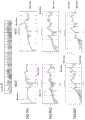
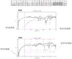
以下,关于这些金属部件10a、10b的串扰降低效果,基于显示模拟结果的一些图表进行详细说明。在此,图7~图11、图13、图15及图21~图23中所示的一系列图表均以纵轴为分贝(dB)、横轴为频率(GHz)而示出了信号速度与串扰的信号强度的关系。Hereinafter, the crosstalk reduction effect of these
图7的图表中,相对于没有设置金属部件10a、10b的(没有GND连接)现有例,示出了设置金属部件10a、10b的(有GND连接)本实施方式中的进行与阻抗的改善效果有关的模拟的结果的一个例子。该图表是关于上排的PIN排列中的信号线(从左起第10个的TX1)和下排的PIN排列中的信号线(从左起第9个的TX2)模拟了近端串扰(Near End X(Cross)Talk;以下简称为“NEXT”。)和远端串扰(Far End X(Cross)Talk;以下简称为“FEXT”。)的结果的一个例子。In the graph of FIG. 7, compared with the conventional example in which the
如图7所示,在上排从左起第10个的TX1和下排从左起第9个的TX2中,因为彼此的距离较近,在NEXT及FEXT的任一个中无论有没有GND连接都看不到串扰上有较大的差异。As shown in Figure 7, in TX1, which is the 10th from the left in the upper row, and TX2, which is the 9th from the left in the lower row, because they are relatively close to each other, no matter whether there is a GND connection in either of NEXT and FEXT No significant difference in crosstalk can be seen.
另一方面,在图8的图表中,同样地,相对于没有设置金属部件10a、10b的(没有GND连接)现有例,示出了设置金属部件10a、10b的(有GND连接)本实施方式中的进行与阻抗的改善效果有关的模拟的结果的一个例子,并且是对于上排的PIN排列之中彼此隔离的信号线,即从左起第3个的RX1和第10个的TX1,模拟了NEXT和FEXT的结果的一个例子。On the other hand, in the graph of FIG. 8 , similarly, with respect to the conventional example in which the
由图8可知,关于NEXT,“有GND连接”的情况下的信号强度总体上低于“没有GND连接”的信号强度的两倍,特别是,在8~9GHz中显著下降,由此可看出本实施方式的情况下串扰得到显著改善。另外,关于FEXT,约7GHz以下“没有GND连接”的情况下存在示出信号强度低的向下尖峰的频带,但是在峰值地点上“有GND连接”时更低,且信号强度在8~9GHz及其周边频带中显著下降,由此也能看出本实施方式的情况下串扰得到改善。As can be seen from Figure 8, with regard to NEXT, the signal strength in the case of "with GND connection" is generally lower than twice the signal strength of "without GND connection", especially, it drops significantly in 8-9GHz. In the case of this embodiment, the crosstalk is significantly improved. In addition, regarding FEXT, there is a frequency band showing a downward spike with low signal strength in the case of "no GND connection" below about 7 GHz, but it is lower when "GND connection" is at the peak point, and the signal strength is 8 to 9 GHz It can also be seen from this that the crosstalk is improved in the case of this embodiment.
图9的图表也同样,示出将没有GND连接的现有例和有GND连接的本实施方式进行对比的模拟结果的一个例子,但是在本例中,是关于上排和下排的PIN排列之中彼此隔离的信号线,即,上排从左起第10个的TX1和下排从左起第2个的RX2,模拟了NEXT和FEXT的结果的一个例子。The graph in FIG. 9 also shows an example of simulation results comparing a conventional example without GND connection and this embodiment with GND connection, but in this example, it is about the upper row and the lower row of PIN arrangement. Among the signal lines isolated from each other, that is, TX1, which is the 10th from the left in the upper row, and RX2, which is the 2nd from the left in the lower row, simulate an example of the results of NEXT and FEXT.
与图8的情况同样,判明了在本实施方式的情况下,对于NEXT及FEXT的任一个都能看出串扰得到改善。As in the case of FIG. 8 , it was found that in the case of the present embodiment, crosstalk was improved in both NEXT and FEXT.
这样,依据本实施方式,具备分别配置在被外壳100的上部外壳100a、下部外壳100b分别支撑的接触件1a-k(k=1~11)及接触件1b-k(k=1~11)的上侧及下侧并短路接地用的接触件的金属部件10a、10b,金属部件10a、10b具有以避开接地用的接触件以外的接触件的方式弯曲的弯曲部,因此提供降低了串扰的高速传输用连接器6。Thus, according to the present embodiment, the
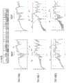
关于金属部件的尺寸及配置场所等Dimensions and placement of metal parts, etc.
1)上侧金属部件的宽度1) Width of upper metal part
上侧金属部件10a的宽度Wa优选在1.0mm至2.5mm之间。The width Wa of the
图10中示出Wa=1.0mm的情况和Wa=2.5mm的情况下的模拟串扰的结果的例子。关于下排从左起第9个的TX2和上排从左起第10个的TX1、上排从左起第10个的TX1和上排从左起第3个的RX1、上排从左起第10个的TX1和下排从左起第2个的RX2分别模拟了NEXT和FEXT。FIG. 10 shows examples of results of simulated crosstalk in the case of Wa=1.0 mm and Wa=2.5 mm. Regarding TX2, which is the 9th from left on the bottom row and TX1, which is the 10th from left on the top row, TX1, which is the 10th from left on the top row, and RX1, which is the 3rd from left on the top row, and which is the 3rd from left on the top row The 10th TX1 and the second RX2 from the left in the lower row simulate NEXT and FEXT respectively.
由图10所示的结果可以看出,在宽度1.0mm和2.5mm,总体上阻抗的特性没有显著变化,但是在TX1和RX1的情况下,NEXT无论在8GHz~18GHz区域之外的低速区域还是高速区域都有显著差异,因此作为上侧金属部件10a的宽度Wa,最好选择2.5mm。From the results shown in Figure 10, it can be seen that the overall impedance characteristics do not change significantly at widths of 1.0mm and 2.5mm, but in the case of TX1 and RX1, NEXT is in the low-speed region outside the 8GHz-18GHz region or There is a significant difference in the high-speed region, so it is preferable to select 2.5 mm as the width Wa of the
2)下侧金属部件的宽度2) Width of lower metal parts
下侧金属部件10b的宽度Wb优选在0.5mm至1.0mm之间。The width Wb of the
图11是在Wb=0.5mm的情况和Wb=1.0mm的情况下模拟了串扰的结果的例子。关于TX2和TX1、TX2和RX2、TX2和RX1分别模拟了NEXT和FEXT。FIG. 11 is an example of the results of simulating crosstalk in the case of Wb=0.5 mm and the case of Wb=1.0 mm. NEXT and FEXT are simulated with respect to TX2 and TX1, TX2 and RX2, and TX2 and RX1, respectively.
由图11的图表可知,在TX2和RX1的情况下,由于7~8GHz的峰值在NEXT和FEXT中均得到改善,因此作为下侧金属部件10b的宽度Wb最好选择0.5mm。As can be seen from the graph in FIG. 11, in the case of TX2 and RX1, since the peak of 7-8 GHz is improved in both NEXT and FEXT, it is preferable to select 0.5 mm as the width Wb of the
3)金属部件的(前后)位置3) The (front and rear) position of metal parts
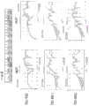
上侧金属部件10a及下侧金属部件10b在前后(X)方向上的设置位置,对于上侧金属部件10a能够在图12所示的从上侧直线部12a到上下(Z)方向直线部13a的下端之间选择任意位置,而对于下侧金属部件10b,可以在图12所示的从下侧直线部12b到Z方向直线部13b的下端之间进行任意设定。The installation positions of the upper
上侧金属部件10a优选配置在上侧直线部12a的中间附近,下侧金属部件10b优选配置在下侧直线部12b的中间附近。在该情况下,上侧金属部件10a及下侧金属部件10b设置成中间隔着上侧直线部12a及下侧直线部12b而大致对置。The
在图4的P1和图12的P2的金属部件的安装位置,关于TX1和TX2、TX1和RX1、TX1和RX2分别模拟了NEXT和FEXT,如图13的由标号P2、P1分别指示的图表所示,8GHz以上的频带上串扰导致的噪声值在上侧直线部12a的大致中央和其大致正下方的下侧直线部12b下表面的位置P1(图4)大体小于直线部13a、13b的下端及其跟前的位置P2(图12),可判断为具有良好的特性。At the installation positions of the metal parts of P1 in FIG. 4 and P2 in FIG. 12 , NEXT and FEXT are respectively simulated with respect to TX1 and TX2, TX1 and RX1, and TX1 and RX2, as shown in the charts indicated by the symbols P2 and P1 respectively in FIG. 13 It shows that the noise value caused by crosstalk in the frequency band above 8 GHz is substantially smaller than the position P1 ( FIG. 4 ) of the lower surface of the lower
4)连接的GND的数量4) The number of connected GND
作为利用金属部件10a、10b进行的GND的连接数量,除了如图3所示连接全部GND的情况之外,也可以如图14所示的金属部件10a-a、10a-b那样仅连接一部分GND。金属部件10a-a具有弯曲部10a-a1和与弯曲部10a-a1相连并从弯曲部10a-a1沿列方向(±Y方向)延伸的基底部10a-a21及基底部10a-a22。基底部10a-a21及基底部10a-a22分别与接触件1a-11(G)及1a-9(G)的各上表面相接,从而与这些电连接,另一方面,弯曲部10a-a1与接触件1a-10(S)隔离。同样地,金属部件10a-b具有弯曲部10a-b1和与弯曲部10a-b1并从弯曲部10a-b1沿列方向(±Y方向)延伸的基底部10a-b21及基底部10a-b22。基底部10a-b21及基底部10a-b22分别与接触件1a-2(G)及1a-4(G)的各上表面相接,从而与这些电连接,另一方面,弯曲部10a-b1与接触件1a-3(S)隔离。As the number of GND connections made by the
然而,由图15的图表所示的模拟结果可知,串扰导致的噪声值在连接所有GND时大体低于仅连接一部分GND时,特别是在约8GHz以上的带域上可看到显著差异,因此可以判断为具有良好的特性。However, from the simulation results shown in the graph of Fig. 15, it can be seen that the noise value due to crosstalk is generally lower when all GNDs are connected than when only some GNDs are connected, and a significant difference can be seen especially in the band above about 8 GHz. It can be judged that it has favorable characteristics.
5)金属部件的对数5) Logarithm of metal parts
金属部件10a、10b的对数,并不限于如图4所示一对,例如也可以如图16所示设置多对。然而,虽然没有特别图示,但是当模拟了串扰时,可知两者的差异较小,从制造成本等的观点来看,可以说金属部件10a、10b的对数优选为一对。The number of pairs of
6)金属部件的弯曲部的高度6) The height of the bent part of the metal part
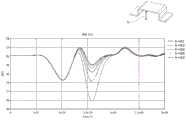
图17中示出使金属部件10a、10b中的各个弯曲部的高度(从对置的接触件表面起的距离)h在0.1mm到0.5mm之间变化时的阻抗特性的模拟结果的一个例子。如该图所示,在如h=0.1mm那样金属部件非常接近接触件的情况下,阻抗值下降太多,但当弯曲部的高度h在0.2mm到0.5mm之间时,示出阻抗特性的差异较少,可知在该数值范围内可以选择任意值。FIG. 17 shows an example of the simulation results of impedance characteristics when the height (distance from the opposing contact surface) h of each bent portion of the
(2)第2实施方式(2) Second embodiment
在上述的第1实施方式中举出将金属部件10a、10b适用于单端传输型连接器的情况进行了说明,但是上述的金属部件并不限于此,即便适用于差分传输型(DeferentialSignaling Type)连接器,也能进一步降低串扰。以下,参照附图,对差分传输型的适用例进行说明。In the above-mentioned first embodiment, the case where the
本实施方式的高速传输用连接器16中的外壳、通信对象的光收发器15所嵌合的插槽、以及接触件1a-k(k=1~11)和接触件1b-k(k=1~11)的包括形状、尺寸在内的详细结构,基本上与第1实施方式的高速传输用连接器6相同,因此,省略详细的说明,以下主要以与第1实施方式的区别点为中心进行说明。The housing in the high-
高速传输用连接器16为差分传输型,因此插槽中的光收发器15的PIN配置与上述的第1实施方式不同。如图18所示,在本实施方式中上侧下侧的第1~第11PIN排列配置成如下。The high-
关于上侧,接地GND被分配到左端的第1PIN、从左端起第4~第8PIN的列及右端的PIN的列的每一个上。接收信号RX1-n被分配到从左端起第2个的第2PIN,接收信号RX1-p被分配到从左端起第3个的第3PIN,发送信号TX1-n被分配到从左端起第9个的第9PIN,发送信号用TX1-p被分配到从左端起第10个的第10PIN。With respect to the upper side, the ground GND is distributed to each of the first PIN at the left end, the row of 4th to 8th PINs from the left end, and the row of PINs at the right end. The received signal RX1-n is assigned to the 2nd pin from the left end, the received signal RX1-p is assigned to the 3rd pin from the left end, and the transmitted signal TX1-n is assigned to the 9th pin from the left end The 9th PIN of the TX1-p for transmission signal is assigned to the 10th PIN which is the 10th from the left end.
关于下侧也同样,接地GND被分配到左端的第1PIN、从左端起第4~第8PIN的列及右端的PIN的每一个上。接收信号RX2-n被分配到从左端起第2个的第2PIN,接收信号RX2-p被分配到从左端起第3个的第3PIN,发送信号TX2-n被分配到从左端起第9个的第9PIN,发送信号TX2-p被分配到从左端起第10个的第10PIN。Also on the lower side, the ground GND is assigned to the first PIN at the left end, the column of the fourth to eighth PINs from the left end, and each of the PINs at the right end. The received signal RX2-n is assigned to the 2nd pin from the left end, the received signal RX2-p is assigned to the 3rd pin from the left end, and the transmitted signal TX2-n is assigned to the 9th pin from the left end The 9th PIN of , and the transmission signal TX2-p are allocated to the 10th PIN 10th from the left end.
对应于上述的PIN排列,金属部件的形状也与第1实施方式的形状不同。即,如图19所示,本实施方式的高速传输用连接器16所具备的金属部件20a具有基底部20a-21~20a-23及弯曲部20a-1和20a-2并且在接触件1a-k的列的各直线部12a上沿左右(Y方向)配置,基底部20a-21~20a-23与第1~第11PIN的列之中与接地GND连接的接触件1a-k从其上表面相接而电连接,而以避开除这些接触件以外的其他接触件1a-k的方式,弯曲部20a-1和20a-2分别配置成以呈上下倒置U字形的方式向上方弯曲。基底部20a-21、20a-22与弯曲部20a-1相连并从弯曲部20a-1沿列方向(±Y方向)延伸,基底部20a-22还与弯曲部20a-2相连,基底部20a-23与弯曲部20a-2相连并沿列方向(-Y方向)延伸。Corresponding to the above-mentioned PIN arrangement, the shape of the metal member is also different from that of the first embodiment. That is, as shown in FIG. 19 , the
更具体而言,如图19所示,金属部件20a在基底部20a-21~20a-23与接触件1a-1(G)、1a-4(G)~1a-8(G)及1a-11(G)从各自的上表面接触而将这些彼此电连接,另一方面,对于接触件1a-2(S)、1a-3(S),使弯曲部20a-1从这些接触件向上方隔离,并且对于接触件1a-9(S)、1a-10(S),使弯曲部20a-2从这些接触件沿上方隔离,由此以使这些接触件成为非电连接的方式避免接触。进一步具体而言,第1弯曲部20a-1与分别传输接收信号RX1-n、RX1-p的接触件1a-2(S)、1a-3(S)隔离,第2弯曲部20a-2与传输发送信号TX1-n、TX1-p的接触件1a-9(S)、1a-10(S)隔离。More specifically, as shown in FIG. 19 , the
金属部件20a的材料及对第1~第11PIN排列的安装方法与上述的第1实施方式的金属部件10a相同。The material of the
接着,对安装在接触件1b-k(k=1~11)侧的金属部件20b进行说明。Next, the
如图20所示,本实施方式的高速传输用连接器16所具备的金属部件20b具有基底部20b-21、20b-22、20b-23和弯曲部20b-1、20b-2,配置成在接触件1b-k的列的各直线部12b的下表面沿左右(±Y方向)延伸,在基底部20b-21、20b-22、20b-23与跟接地用接触件GND连接的接触件1b-k在下表面相接而电连接,弯曲部20b-1、20b-2配置成以避开除这些接触件以外的其他接触件1b-k的方式与这些其他接触件隔离并向下侧以大致“U”字状弯曲。基底部20b-21、20b-22与弯曲部20b-1相连并沿列方向(±Y方向)延伸。基底部20b-22在列方向(-Y方向)上还与弯曲部20b-2相连,基底部20b-23与弯曲部20b-2相连并沿列方向(-Y方向)延伸。As shown in FIG. 20 , the
更具体而言,金属部件20b在基底部20b-21、20b-22、20b-23与接触件1b-1(G)、1b-4(G)~1b-8(G)及1b-11(G)在这些接触件的各下表面接触而使这些彼此电连接,对于接触件1b-2(S)、1b-3(S)、1b-9(S)、1b-10(S),弯曲部20b-1配置成与这些接触件的下方隔离,由此,以使这些接触件1b-2(S)、1b-3(S)、1b-9(S)、1b-10(S)成为非电连接的方式避免彼此接触。进一步具体而言,第1弯曲部20b-1与分别传输接收信号RX2-n、RX2-p的接触件1b-2(S)、1b-3(S)隔离,第2弯曲部20b-2与分别传输发送信号TX2-n、TX2-p的接触件1b-9(S)、1b-10(S)隔离。More specifically, the
金属部件20b的材料及对第1~第11PIN排列的安装方法也与上述的第1实施方式的金属部件10b相同。The material of the
此外,高速传输用连接器16为差分传输型,因此无论通信对象的光收发器15还是接触件1a-k(k=1~11)及接触件1b-k(k=1~11)所连接的电路基板S2都与第1实施方式不同。插槽40中嵌合光收发器5的头部17,接触件1a-k(k=1~11)及接触件1b-k(k=1~11)的基板侧接触部14a、14b,例如通过焊接连接到具有对应的布线的外部的电路基板S2的接触件。In addition, the high-
以下,根据模拟结果,详细说明本实施方式中的利用金属部件20a、20b得到的串扰降低效果。Hereinafter, the effect of reducing crosstalk obtained by using the
图21的图表中,相对于没有设置金属部件20a、20b的(没有GND连接)现有例,示出了设置金属部件20a、20b的(有GND连接)本实施方式的进行与串扰的改善效果有关的模拟结果的一个例子。该图表是关于上排的PIN排列中的信号线(从左起第9个的TX1-n及第10个的TX1-p)和下排的PIN排列中的信号线(从左起第9个的TX2-n及第10个的TX2-p)模拟了NEXT和FEXT的结果的一个例子。In the graph of FIG. 21 , compared to the conventional example in which the
如图21所示,由于上排的TX1-n及TX1-p与下排的TX2-n及TX2-p彼此的距离较近,与上述的第1实施方式同样,在NEXT及FEXT的任一个中无论有没有GND连接都看不到串扰上有较大的差异。As shown in FIG. 21 , since the distances between TX1-n and TX1-p on the upper row and TX2-n and TX2-p on the lower row are relatively close, similar to the first embodiment described above, in either of NEXT and FEXT No significant difference in crosstalk is seen with or without the GND connection.
另一方面,在图22的图表中,同样地,相对于没有设置金属部件20a、20b的(没有GND连接)现有例,示出了设置金属部件20a、20b的(有GND连接)本实施方式中进行的与串扰的改善效果有关的模拟结果的另一个例子,并且是对于上排的PIN排列之中彼此隔离的信号线,即从左起第2个的RX1-n及第3个的RX1-p与第9个的TX1-n及第10个的TX1-p,模拟了NEXT和FEXT的结果的一个例子。On the other hand, in the graph of FIG. 22 , similarly, with respect to the conventional example in which the
由图22判明了关于NEXT及FEXT两者,除了仅12~15GHz的区域及25GHz以上的区域以外,“有GND连接”的情况下的信号强度显著低于“没有GND连接”的情况,可看出本实施方式的情况下串扰得到显著改善。From Fig. 22, it is clear that for both NEXT and FEXT, except for only the 12-15GHz area and the area above 25GHz, the signal strength in the case of "with GND connection" is significantly lower than that of "without GND connection". In the case of this embodiment, the crosstalk is significantly improved.
图23的图表也同样,相对于没有GND连接的现有例,示出了将有GND连接的本实施方式进行对比的模拟结果的另一个例子,但是在本例中,是关于上排和下排的PIN排列之中彼此隔离的信号线,即上排中从左起第9个的TX1-n及第10个的TX1-p与下排中从左起第2个的RX2-n及第3个的RX2-p,模拟了NEXT和FEXT的结果的一个例子。The graph of Fig. 23 also shows another example of simulation results comparing this embodiment with GND connection with respect to the conventional example without GND connection, but in this example, it is about the upper row and the lower row The signal lines isolated from each other in the PIN arrangement of the first row, that is, the TX1-n and the 10th TX1-p from the left in the upper row and the RX2-n and the RX2-n and the 10th from the left in the
与图22的情况同样,判明了在本实施方式的情况下,对于NEXT及FEXT两者能看出串扰总体上得到改善。As in the case of FIG. 22 , it was found that in the case of the present embodiment, crosstalk is generally improved for both NEXT and FEXT.
关于第2实施方式,金属部件20a、20b的宽度、厚度、从各接触件到弯曲部为止的距离等的形状、尺寸以及配置位置、对数、连续/非连续的区别等,实质上也与上述的第1实施方式相同。因此,省略详细的说明。Regarding the second embodiment, the shape, size, arrangement position, logarithm, distinction of continuous/non-continuous, etc. of the width and thickness of the
这样,对于本实施方式的差分传输型的高速传输用连接器16,也具备配置在接触件1a-k(k=1~11)及接触件1b-k(k=1~11)的上侧及下侧并将接地用的接触件短路的金属部件20a、20b,这些金属部件20a、20b具有以避开接地用的接触件以外的接触件的方式弯曲的弯曲部,因此能够进一步降低串扰。In this way, the differential transmission type high-
变形例Variation
以上,说明了本发明的实施方式,但是也可以对该实施方式加入以下的变形。As mentioned above, although embodiment of this invention was described, the following deformation|transformation may be added to this embodiment.
上述实施方式中,对金属部件10a、10b或20a、20b全部成对具备的方式进行了说明,但并不限于此,在不是成对而仅具备任一个的情况下也能降低串扰。In the above-mentioned embodiment, the form in which all the
另外,关于接触件1a-k及1b-k的根数,在上述实施方式中举出了11根的情况,但并不限于此,显然,无论在具有10根以下还是具有12根以上的情况下都能适用本发明。In addition, regarding the number of
进而,关于PIN排列,也举出了在发送与接收之间配置4根~5根GND接触件的例子,但该根数不是必须的,既可以配置更少根数的GND接触件,也可以配置更多个GND接触件。Furthermore, regarding the PIN arrangement, an example of disposing 4 to 5 GND contacts between transmission and reception is also given, but this number is not essential, and a smaller number of GND contacts can be arranged, or Configure more GND contacts.
以上,一边参照附图一边说明了本发明的实施方式,但是这些是为了便于理解发明,不能以这些限定本发明的权利要求。The embodiments of the present invention have been described above with reference to the drawings, but these are for facilitating understanding of the invention, and the claims of the present invention should not be limited by these.
在不脱离本发明的范围及要旨的范围内,本领域技术人员可以加入各种变更而实现本发明,例如,可以将一个实施例的特征结合到其他实施例,从而得到另一个实施例。本领域技术人员可以根据本发明的要旨,在不脱离权利要求的范围内进行各种变更、等同置换或改良等。Without departing from the scope and gist of the present invention, those skilled in the art can add various changes to realize the present invention. For example, the features of one embodiment can be combined with other embodiments to obtain another embodiment. Those skilled in the art can make various changes, equivalent replacements, or improvements based on the gist of the present invention without departing from the scope of the claims.
标号说明Label description
100外壳;100a上部外壳;100b下部外壳;1a-k(k=1~11)(第1)接触件;1b-k(k=1~11)(第2)接触件;10a、10b、20a、20b金属部件;10a-1、10a-2、10a-3弯曲部;10a-21、10a-22、10a-23、10a-24基底部;10b-1、10b-2、10b-3、10b-4弯曲部;10b-21、10b-22、10b-23、10b-24基底部;10a-a1、10a-b1弯曲部;10a-a21、10a-a22、10a-b21、10a-b22基底部;11a、11b前端侧接触部;12a、12b、13a、13b直线部;14a、14b基板侧接触部。100 shell; 100a upper shell; 100b lower shell; 1a-k (k=1~11) (1st) contact piece; 1b-k (k=1~11) (2nd) contact piece; 10a, 10b, 20a , 20b metal parts; 10a-1, 10a-2, 10a-3 bending part; 10a-21, 10a-22, 10a-23, 10a-24 base part; 10b-1, 10b-2, 10b-3, 10b -4 bend; 10b-21, 10b-22, 10b-23, 10b-24 base; 10a-a1, 10a-b1 bend; 10a-a21, 10a-a22, 10a-b21, 10a-b22 base ; 11a, 11b front end side contact portion; 12a, 12b, 13a, 13b straight line portion; 14a, 14b substrate side contact portion.
Claims (8)
Priority Applications (2)
| Application Number | Priority Date | Filing Date | Title |
|---|---|---|---|
| CN202111289444.8ACN116073156A (en) | 2021-11-02 | 2021-11-02 | Connectors for high-speed transmission |
| US17/976,332US12407136B2 (en) | 2021-11-02 | 2022-10-28 | Connector for high-speed transmission |
Applications Claiming Priority (1)
| Application Number | Priority Date | Filing Date | Title |
|---|---|---|---|
| CN202111289444.8ACN116073156A (en) | 2021-11-02 | 2021-11-02 | Connectors for high-speed transmission |
Publications (1)
| Publication Number | Publication Date |
|---|---|
| CN116073156Atrue CN116073156A (en) | 2023-05-05 |
Family
ID=86144973
Family Applications (1)
| Application Number | Title | Priority Date | Filing Date |
|---|---|---|---|
| CN202111289444.8APendingCN116073156A (en) | 2021-11-02 | 2021-11-02 | Connectors for high-speed transmission |
Country Status (2)
| Country | Link |
|---|---|
| US (1) | US12407136B2 (en) |
| CN (1) | CN116073156A (en) |
Families Citing this family (1)
| Publication number | Priority date | Publication date | Assignee | Title |
|---|---|---|---|---|
| TWI819829B (en)* | 2022-09-30 | 2023-10-21 | 宏致電子股份有限公司 | Electrical connector |
Family Cites Families (12)
| Publication number | Priority date | Publication date | Assignee | Title |
|---|---|---|---|---|
| JP3987493B2 (en)* | 2001-08-01 | 2007-10-10 | モレックス インコーポレーテッド | Impedance adjusted connector |
| US8764464B2 (en)* | 2008-02-29 | 2014-07-01 | Fci Americas Technology Llc | Cross talk reduction for high speed electrical connectors |
| JP5405582B2 (en) | 2008-11-14 | 2014-02-05 | モレックス インコーポレイテド | Resonance change connector |
| JP5019187B2 (en)* | 2010-01-29 | 2012-09-05 | 山一電機株式会社 | connector |
| US8353726B2 (en)* | 2010-11-03 | 2013-01-15 | Hon Hai Precision Inc. Co., Ltd. | Electrical connector with grounding bars therein to reduce cross talking |
| CN202076606U (en)* | 2011-05-03 | 2011-12-14 | 富士康(昆山)电脑接插件有限公司 | Electric connector |
| SG186504A1 (en)* | 2011-06-10 | 2013-01-30 | Tyco Electronics Singapore Pte Ltd | Cross talk reduction for a high speed electrical connector |
| EP2541696A1 (en)* | 2011-06-29 | 2013-01-02 | Tyco Electronics Belgium EC BVBA | Electrical connector |
| JP6007146B2 (en)* | 2012-04-27 | 2016-10-12 | 第一電子工業株式会社 | connector |
| JP2016181529A (en)* | 2012-04-27 | 2016-10-13 | 第一電子工業株式会社 | connector |
| US8944849B1 (en)* | 2013-07-25 | 2015-02-03 | Hon Hai Precision Industry Co., Ltd. | Electrical connector with two ground bars connecting each other |
| US9692183B2 (en)* | 2015-01-20 | 2017-06-27 | Te Connectivity Corporation | Receptacle connector with ground bus |
- 2021
- 2021-11-02CNCN202111289444.8Apatent/CN116073156A/enactivePending
- 2022
- 2022-10-28USUS17/976,332patent/US12407136B2/enactiveActive
Also Published As
| Publication number | Publication date |
|---|---|
| US12407136B2 (en) | 2025-09-02 |
| US20230134664A1 (en) | 2023-05-04 |
Similar Documents
| Publication | Publication Date | Title |
|---|---|---|
| CN109786996B (en) | Receptacle Connector Assemblies for Electronic Packaging | |
| US7131862B2 (en) | Electrical connector with horizontal ground plane | |
| JP4717020B2 (en) | Relay board and optical communication module | |
| CN102394398B (en) | Connector assembly having a mating adapter | |
| US8142207B1 (en) | QSFP receptacle with grounding plate and noise cancellation | |
| CN101453088A (en) | electrical connector | |
| US20120129396A1 (en) | Plug connector having multiple circuit boards and method of making the same | |
| CN112909659B (en) | Wire Harnesses, Connections and Connectors | |
| CN207098133U (en) | Electric coupler component | |
| CN112290334B (en) | Interposer with a plurality of pins | |
| EP2197073B1 (en) | High frequency circuit module | |
| JP2015026652A (en) | Flexible substrate | |
| US20070173116A1 (en) | Multipolar connector and portable radio terminal or small-sized electronic device using multipolar connector | |
| CN215266745U (en) | Connector assembly | |
| CN100479267C (en) | High-frequency connector | |
| CN116073156A (en) | Connectors for high-speed transmission | |
| JP2011249215A (en) | Substrate and ic socket | |
| CN207038759U (en) | Electric connector assembly and switching circuit board thereof | |
| US11050200B2 (en) | Electrical connector with hermaphroditic terminal and housing | |
| JP2009252918A (en) | Optical data link | |
| CN113966647A (en) | Multilayer circuit board | |
| CN202564681U (en) | Electrical connector | |
| CN116259990A (en) | Connector and wire harness | |
| CN201142393Y (en) | electrical connector | |
| CN113179579A (en) | Circuit board and electronic equipment |
Legal Events
| Date | Code | Title | Description |
|---|---|---|---|
| PB01 | Publication | ||
| PB01 | Publication | ||
| SE01 | Entry into force of request for substantive examination | ||
| SE01 | Entry into force of request for substantive examination |