CN116072542A - Preparation method of ring grid TFET device - Google Patents
Preparation method of ring grid TFET deviceDownload PDFInfo
- Publication number
- CN116072542A CN116072542ACN202211533675.3ACN202211533675ACN116072542ACN 116072542 ACN116072542 ACN 116072542ACN 202211533675 ACN202211533675 ACN 202211533675ACN 116072542 ACN116072542 ACN 116072542A
- Authority
- CN
- China
- Prior art keywords
- layer
- film layer
- gate
- etching
- channel
- Prior art date
- Legal status (The legal status is an assumption and is not a legal conclusion. Google has not performed a legal analysis and makes no representation as to the accuracy of the status listed.)
- Pending
Links
Images


Classifications
- H—ELECTRICITY
- H10—SEMICONDUCTOR DEVICES; ELECTRIC SOLID-STATE DEVICES NOT OTHERWISE PROVIDED FOR
- H10D—INORGANIC ELECTRIC SEMICONDUCTOR DEVICES
- H10D64/00—Electrodes of devices having potential barriers
- H10D64/01—Manufacture or treatment
- H10D64/017—Manufacture or treatment using dummy gates in processes wherein at least parts of the final gates are self-aligned to the dummy gates, i.e. replacement gate processes
- H—ELECTRICITY
- H10—SEMICONDUCTOR DEVICES; ELECTRIC SOLID-STATE DEVICES NOT OTHERWISE PROVIDED FOR
- H10D—INORGANIC ELECTRIC SEMICONDUCTOR DEVICES
- H10D48/00—Individual devices not covered by groups H10D1/00 - H10D44/00
- H10D48/383—Quantum effect devices, e.g. of devices using quantum reflection, diffraction or interference effects
- H—ELECTRICITY
- H10—SEMICONDUCTOR DEVICES; ELECTRIC SOLID-STATE DEVICES NOT OTHERWISE PROVIDED FOR
- H10D—INORGANIC ELECTRIC SEMICONDUCTOR DEVICES
- H10D12/00—Bipolar devices controlled by the field effect, e.g. insulated-gate bipolar transistors [IGBT]
- H10D12/01—Manufacture or treatment
- H—ELECTRICITY
- H10—SEMICONDUCTOR DEVICES; ELECTRIC SOLID-STATE DEVICES NOT OTHERWISE PROVIDED FOR
- H10D—INORGANIC ELECTRIC SEMICONDUCTOR DEVICES
- H10D12/00—Bipolar devices controlled by the field effect, e.g. insulated-gate bipolar transistors [IGBT]
- H10D12/01—Manufacture or treatment
- H10D12/021—Manufacture or treatment of gated diodes, e.g. field-controlled diodes [FCD]
- H—ELECTRICITY
- H10—SEMICONDUCTOR DEVICES; ELECTRIC SOLID-STATE DEVICES NOT OTHERWISE PROVIDED FOR
- H10D—INORGANIC ELECTRIC SEMICONDUCTOR DEVICES
- H10D12/00—Bipolar devices controlled by the field effect, e.g. insulated-gate bipolar transistors [IGBT]
- H10D12/211—Gated diodes
- H—ELECTRICITY
- H10—SEMICONDUCTOR DEVICES; ELECTRIC SOLID-STATE DEVICES NOT OTHERWISE PROVIDED FOR
- H10D—INORGANIC ELECTRIC SEMICONDUCTOR DEVICES
- H10D12/00—Bipolar devices controlled by the field effect, e.g. insulated-gate bipolar transistors [IGBT]
- H10D12/411—Insulated-gate bipolar transistors [IGBT]
- H—ELECTRICITY
- H10—SEMICONDUCTOR DEVICES; ELECTRIC SOLID-STATE DEVICES NOT OTHERWISE PROVIDED FOR
- H10D—INORGANIC ELECTRIC SEMICONDUCTOR DEVICES
- H10D30/00—Field-effect transistors [FET]
- H10D30/01—Manufacture or treatment
- H10D30/014—Manufacture or treatment of FETs having zero-dimensional [0D] or one-dimensional [1D] channels, e.g. quantum wire FETs, single-electron transistors [SET] or Coulomb blockade transistors
- H—ELECTRICITY
- H10—SEMICONDUCTOR DEVICES; ELECTRIC SOLID-STATE DEVICES NOT OTHERWISE PROVIDED FOR
- H10D—INORGANIC ELECTRIC SEMICONDUCTOR DEVICES
- H10D30/00—Field-effect transistors [FET]
- H10D30/40—FETs having zero-dimensional [0D], one-dimensional [1D] or two-dimensional [2D] charge carrier gas channels
- H10D30/43—FETs having zero-dimensional [0D], one-dimensional [1D] or two-dimensional [2D] charge carrier gas channels having 1D charge carrier gas channels, e.g. quantum wire FETs or transistors having 1D quantum-confined channels
- H—ELECTRICITY
- H10—SEMICONDUCTOR DEVICES; ELECTRIC SOLID-STATE DEVICES NOT OTHERWISE PROVIDED FOR
- H10D—INORGANIC ELECTRIC SEMICONDUCTOR DEVICES
- H10D30/00—Field-effect transistors [FET]
- H10D30/60—Insulated-gate field-effect transistors [IGFET]
- H10D30/67—Thin-film transistors [TFT]
- H10D30/6729—Thin-film transistors [TFT] characterised by the electrodes
- H10D30/673—Thin-film transistors [TFT] characterised by the electrodes characterised by the shapes, relative sizes or dispositions of the gate electrodes
- H10D30/6735—Thin-film transistors [TFT] characterised by the electrodes characterised by the shapes, relative sizes or dispositions of the gate electrodes having gates fully surrounding the channels, e.g. gate-all-around
- H—ELECTRICITY
- H10—SEMICONDUCTOR DEVICES; ELECTRIC SOLID-STATE DEVICES NOT OTHERWISE PROVIDED FOR
- H10D—INORGANIC ELECTRIC SEMICONDUCTOR DEVICES
- H10D30/00—Field-effect transistors [FET]
- H10D30/60—Insulated-gate field-effect transistors [IGFET]
- H10D30/67—Thin-film transistors [TFT]
- H10D30/6757—Thin-film transistors [TFT] characterised by the structure of the channel, e.g. transverse or longitudinal shape or doping profile
- H—ELECTRICITY
- H10—SEMICONDUCTOR DEVICES; ELECTRIC SOLID-STATE DEVICES NOT OTHERWISE PROVIDED FOR
- H10D—INORGANIC ELECTRIC SEMICONDUCTOR DEVICES
- H10D62/00—Semiconductor bodies, or regions thereof, of devices having potential barriers
- H10D62/10—Shapes, relative sizes or dispositions of the regions of the semiconductor bodies; Shapes of the semiconductor bodies
- H10D62/117—Shapes of semiconductor bodies
- H10D62/118—Nanostructure semiconductor bodies
- H10D62/119—Nanowire, nanosheet or nanotube semiconductor bodies
- H10D62/121—Nanowire, nanosheet or nanotube semiconductor bodies oriented parallel to substrates
- H—ELECTRICITY
- H10—SEMICONDUCTOR DEVICES; ELECTRIC SOLID-STATE DEVICES NOT OTHERWISE PROVIDED FOR
- H10D—INORGANIC ELECTRIC SEMICONDUCTOR DEVICES
- H10D62/00—Semiconductor bodies, or regions thereof, of devices having potential barriers
- H10D62/10—Shapes, relative sizes or dispositions of the regions of the semiconductor bodies; Shapes of the semiconductor bodies
- H10D62/17—Semiconductor regions connected to electrodes not carrying current to be rectified, amplified or switched, e.g. channel regions
- H10D62/213—Channel regions of field-effect devices
- H10D62/221—Channel regions of field-effect devices of FETs
- H10D62/235—Channel regions of field-effect devices of FETs of IGFETs
- H—ELECTRICITY
- H10—SEMICONDUCTOR DEVICES; ELECTRIC SOLID-STATE DEVICES NOT OTHERWISE PROVIDED FOR
- H10D—INORGANIC ELECTRIC SEMICONDUCTOR DEVICES
- H10D64/00—Electrodes of devices having potential barriers
- H10D64/01—Manufacture or treatment
- H10D64/018—Spacers formed inside holes at the prospective gate locations, e.g. holes left by removing dummy gates
- H—ELECTRICITY
- H10—SEMICONDUCTOR DEVICES; ELECTRIC SOLID-STATE DEVICES NOT OTHERWISE PROVIDED FOR
- H10D—INORGANIC ELECTRIC SEMICONDUCTOR DEVICES
- H10D64/00—Electrodes of devices having potential barriers
- H10D64/01—Manufacture or treatment
- H10D64/021—Manufacture or treatment using multiple gate spacer layers, e.g. bilayered sidewall spacers
- H—ELECTRICITY
- H10—SEMICONDUCTOR DEVICES; ELECTRIC SOLID-STATE DEVICES NOT OTHERWISE PROVIDED FOR
- H10D—INORGANIC ELECTRIC SEMICONDUCTOR DEVICES
- H10D64/00—Electrodes of devices having potential barriers
- H10D64/20—Electrodes characterised by their shapes, relative sizes or dispositions
- H10D64/27—Electrodes not carrying the current to be rectified, amplified, oscillated or switched, e.g. gates
- H10D64/311—Gate electrodes for field-effect devices
- H10D64/411—Gate electrodes for field-effect devices for FETs
- H10D64/511—Gate electrodes for field-effect devices for FETs for IGFETs
- H10D64/512—Disposition of the gate electrodes, e.g. buried gates
- B—PERFORMING OPERATIONS; TRANSPORTING
- B82—NANOTECHNOLOGY
- B82Y—SPECIFIC USES OR APPLICATIONS OF NANOSTRUCTURES; MEASUREMENT OR ANALYSIS OF NANOSTRUCTURES; MANUFACTURE OR TREATMENT OF NANOSTRUCTURES
- B82Y10/00—Nanotechnology for information processing, storage or transmission, e.g. quantum computing or single electron logic
- H—ELECTRICITY
- H10—SEMICONDUCTOR DEVICES; ELECTRIC SOLID-STATE DEVICES NOT OTHERWISE PROVIDED FOR
- H10D—INORGANIC ELECTRIC SEMICONDUCTOR DEVICES
- H10D30/00—Field-effect transistors [FET]
- H10D30/01—Manufacture or treatment
- H10D30/019—Manufacture or treatment of FETs having stacked nanowire, nanosheet or nanoribbon channels
- H—ELECTRICITY
- H10—SEMICONDUCTOR DEVICES; ELECTRIC SOLID-STATE DEVICES NOT OTHERWISE PROVIDED FOR
- H10D—INORGANIC ELECTRIC SEMICONDUCTOR DEVICES
- H10D30/00—Field-effect transistors [FET]
- H10D30/501—FETs having stacked nanowire, nanosheet or nanoribbon channels
Landscapes
- Insulated Gate Type Field-Effect Transistor (AREA)
- Electrodes Of Semiconductors (AREA)
- Thin Film Transistor (AREA)
Abstract
Description
Translated fromChinese技术领域technical field
本发明涉及半导体器件制备技术领域,尤其涉及一种环珊TFET器件的制备方法。The invention relates to the technical field of semiconductor device preparation, in particular to a method for preparing a ring TFET device.
背景技术Background technique
5纳米以下集成电路技术中现有的FinFET器件结构面临诸多挑战。环栅纳米线器件由于具有更好的沟道静电完整性、漏电流控制和载流子一维弹道输运等优势,被认为是延续摩尔定律的关键架构之一。近年来,将理想环栅纳米线结构和主流FinFET工艺结合发展下一代集成技术已成为集成电路深入发展的研发关键热点之一。Existing FinFET device structures in integrated circuit technologies below 5nm face many challenges. Due to the advantages of better channel electrostatic integrity, leakage current control and one-dimensional ballistic transport of carriers, the gate-all-around nanowire device is considered to be one of the key architectures to continue Moore's Law. In recent years, the combination of ideal gate-all-around nanowire structure and mainstream FinFET technology to develop next-generation integration technology has become one of the key R&D hotspots for the in-depth development of integrated circuits.
尽管这些先进工艺节点下的器件较过去已有显著的性能提升,但由于持续减小电源电压的难度增加、器件泄漏电流的增大及亚阈值摆幅受限于60mV/Dec等因素,环栅器件仍面临着高功耗的问题。若要减小器件在关态下的泄漏电流,可以通过降低亚阈值摆幅来实现,其中采用通过带带隧穿(BTBT)的导通原理工作的隧穿场效应晶体管(TFET),从工作原理上打破MOSFET采用热电子发射的导通机理带来的亚阈值摆幅上的限制,从而在关态下具有极小的漏电流。然而,如何将TFET器件与主流的环栅纳米线器件工艺兼容进行制作仍然存在极大的挑战。Although the performance of devices under these advanced process nodes has been significantly improved compared with the past, due to factors such as the difficulty of continuously reducing the supply voltage, the increase of device leakage current, and the sub-threshold swing limited to 60mV/Dec, gate-around The device still faces the problem of high power consumption. To reduce the leakage current of the device in the off-state, it can be achieved by reducing the sub-threshold swing, in which a tunneling field-effect transistor (TFET) that works by the conduction principle of band-band tunneling (BTBT) is used, from the working In principle, it breaks the limitation on the subthreshold swing caused by the conduction mechanism of MOSFET using thermal electron emission, so it has extremely small leakage current in the off state. However, how to make TFET devices compatible with the mainstream gate-all-around nanowire device technology still has great challenges.
发明内容Contents of the invention
本发明提供的环珊TFET器件的制备方法,能够使TFET器件的制备能够兼容环栅器件的制备工艺,实现对环栅TFET器件的批量生产。The preparation method of the surrounding gate TFET device provided by the present invention can make the preparation of the TFET device compatible with the preparation process of the surrounding gate device, and realize the mass production of the surrounding gate TFET device.
本发明提供一种环珊TFET器件的制备方法,所述方法包括:The present invention provides a kind of preparation method of ring TFET device, described method comprises:
在衬底上依次交替形成一个以上的沟道层和一个以上的牺牲层,以形成沟道叠层;Alternately forming more than one channel layer and more than one sacrificial layer on the substrate to form a channel stack;
在衬底上形成跨所述沟道叠层的假栅,并在所述假栅的表面形成第一侧墙;forming a dummy gate across the channel stack on the substrate, and forming a first spacer on the surface of the dummy gate;
对所述牺牲层进行刻蚀,以在所述沟道叠层的侧表面上形成内凹结构,并在所述内凹结构内形成第二侧墙;Etching the sacrificial layer to form a concave structure on a side surface of the channel stack, and forming a second sidewall in the concave structure;
依次制备源漏区域;在制备源极区域时,采用介质材料对漏极区域进行保护,在制备漏极区域时,采用介质材料对源极区域进行保护;Prepare the source and drain regions sequentially; when preparing the source region, use a dielectric material to protect the drain region, and when preparing the drain region, use a dielectric material to protect the source region;
对所述假栅和牺牲层进行刻蚀,以形成环栅制备空间;Etching the dummy gate and the sacrificial layer to form a ring gate preparation space;
在所述环栅制备空间内制备环形的金属栅,以形成环栅TFET器件。A ring-shaped metal gate is prepared in the ring-gate preparation space to form a ring-gate TFET device.
可选地,在衬底上依次交替形成一个以上的沟道层和一个以上的牺牲层,以形成沟道叠层包括:Optionally, sequentially forming more than one channel layer and more than one sacrificial layer alternately on the substrate to form a channel stack includes:
在绝缘体上硅衬底上采用外延的方式交替形成硅锗膜层和硼掺杂的硅膜层,其中,硅锗膜层为牺牲层,硼掺杂的硅膜层为沟道层;Alternately forming silicon-germanium film layers and boron-doped silicon film layers on the silicon-on-insulator substrate by means of epitaxy, wherein the silicon-germanium film layer is a sacrificial layer, and the boron-doped silicon film layer is a channel layer;
采用干法刻蚀工艺对所述沟道叠层进行刻蚀,以形成沿第一方向延伸的鳍片形状的沟道叠层。The channel stack is etched by a dry etching process to form a fin-shaped channel stack extending along the first direction.
可选地,在衬底上形成跨所述沟道叠层的假栅包括:Optionally, forming a dummy gate across the channel stack on the substrate includes:
在所述衬底表面和所述沟道叠层上形成第一膜层;forming a first film layer on the substrate surface and the channel stack;
依据所述沟道叠层的图案形状,对所述第一膜层进行刻蚀,以形成沿第一方向与所述沟道叠层具有台阶,沿第二方向跨过所述沟道叠层的假栅。According to the pattern shape of the channel stack, the first film layer is etched to form a step along the first direction with the channel stack and across the channel stack along the second direction. false grid.
可选地,在所述假栅的表面形成第一侧墙包括:Optionally, forming the first sidewall on the surface of the dummy gate includes:
在所述假栅、沟道叠层以及衬底表面形成第二膜层,其中,所述第二膜层与所述第一膜层具有刻蚀选择比;forming a second film layer on the dummy gate, the channel stack, and the surface of the substrate, wherein the second film layer has an etching selectivity ratio to the first film layer;
对所述第二膜层进行刻蚀,以形成沿第一方向与所述沟道叠层侧表面对齐,围绕所述假栅侧表面并覆盖所述假栅上表面的第一侧墙。Etching the second film layer to form a first sidewall aligned with the side surface of the channel stack along the first direction, surrounding the side surface of the dummy gate and covering the upper surface of the dummy gate.
可选地,对所述牺牲层进行刻蚀,以在所述沟道叠层的侧表面上形成内凹结构包括:Optionally, etching the sacrificial layer to form a concave structure on the side surface of the channel stack includes:
对所述牺牲层暴露的侧壁向内进行刻蚀,以形成内凹结构;其中,刻蚀深度与所述第一侧墙的厚度相等。The exposed sidewall of the sacrificial layer is etched inward to form a concave structure; wherein the etching depth is equal to the thickness of the first sidewall.
可选地,在所述内凹结构内形成第二侧墙包括:Optionally, forming the second side wall in the concave structure includes:
形成第三膜层,所述第三膜层的厚度不小于所述内凹结构的深度;forming a third film layer, the thickness of the third film layer is not less than the depth of the concave structure;
对所述第三膜层进行刻蚀,以形成在第一方向上与所述沟道层对齐的第二侧墙。Etching the third film layer to form a second spacer aligned with the channel layer in the first direction.
可选地,在制备源极区域时,采用介质材料对漏极区域进行保护:Optionally, when preparing the source region, use a dielectric material to protect the drain region:
形成第二膜层;forming a second film layer;
对所述第二膜层进行刻蚀,以使所述源极区域对应的衬底上表面暴露;Etching the second film layer, so that the upper surface of the substrate corresponding to the source region is exposed;
在所述衬底暴露的上表面采用原位掺杂的方式外延形成源极;Epitaxially forming a source on the exposed upper surface of the substrate by in-situ doping;
对所述漏极区域对应的第二膜层进行去除。removing the second film layer corresponding to the drain region.
可选地,在制备漏极区域时,采用介质材料对源极区域进行保护包括:Optionally, when preparing the drain region, using a dielectric material to protect the source region includes:
形成第二膜层;forming a second film layer;
对所述第二膜层进行刻蚀,以使所述漏极区域对应的衬底上表面暴露;Etching the second film layer, so that the upper surface of the substrate corresponding to the drain region is exposed;
在所述衬底暴露的上表面采用原位掺杂的方式外延形成漏极;Epitaxially forming a drain on the exposed upper surface of the substrate by in-situ doping;
对所述源极区域的第二膜层进行去除。removing the second film layer in the source region.
可选地,对所述假栅和牺牲层进行刻蚀,以形成环栅制备空间包括:Optionally, etching the dummy gate and the sacrificial layer to form a ring-ring preparation space includes:
对器件进行平坦化,以去除假栅顶部的第二膜层,暴露所述假栅的上表面;planarizing the device to remove the second film layer on top of the dummy gate to expose the upper surface of the dummy gate;
对所述假栅进行湿法刻蚀,以去除所述假栅,暴露所述牺牲层;performing wet etching on the dummy gate to remove the dummy gate and expose the sacrificial layer;
对所述牺牲层进行化学刻蚀或者原子层刻蚀,以去除所述牺牲层,形成环栅所需的空间。Chemical etching or atomic layer etching is performed on the sacrificial layer to remove the sacrificial layer and form the space required by the ring gate.
可选地,在所述环栅制备空间内制备环形的介质金属栅,以形成环栅TFET器件包括:Optionally, preparing a ring-shaped dielectric metal gate in the ring-gate preparation space to form a ring-gate TFET device includes:
采用原子层沉积或者气相沉积的方式,所述环形栅制备空间内形成环形的介质金属栅。By means of atomic layer deposition or vapor deposition, a ring-shaped dielectric metal grid is formed in the ring-shaped gate preparation space.
在发明提供的技术方案中,通过沟道叠层的设置,将假栅与牺牲层进行配合,提供了TFET器件的前期结构,在制备源漏区域时,通过对源漏的依次制备,并在制备源极时对漏极进行覆盖保护,在制备漏极时对源极进行覆盖保护,实现了TFET器件的源漏制备,最后通过对假栅以及牺牲层的去除和介质金属栅的制备,为源漏之间的沟道层提供了环栅。通过本发明提供的技术方案,能够将TFET器件与环栅器件的生产工艺相兼容,实现环栅TFET器件的批量生产,有效的提高了生产效率。In the technical solution provided by the invention, through the arrangement of the channel stack, the dummy gate is matched with the sacrificial layer to provide the early structure of the TFET device. When preparing the source and drain regions, the source and drain are sequentially prepared, and in the The drain is covered and protected when the source is prepared, and the source is covered and protected when the drain is prepared, realizing the preparation of the source and drain of the TFET device. Finally, by removing the dummy gate and the sacrificial layer and preparing the dielectric metal gate, for The channel layer between the source and drain provides the gate-all-around. Through the technical solution provided by the invention, the production process of the TFET device and the gate-around device can be compatible, and the mass production of the gate-around TFET device can be realized, thereby effectively improving the production efficiency.
附图说明Description of drawings
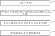
图1为本发明一实施例环珊TFET器件的制备方法的流程图;Fig. 1 is the flow chart of the preparation method of ring TFET device of an embodiment of the present invention;
图2为本发明另一实施例环珊TFET器件的制备方法制备沟道叠层的流程图;Fig. 2 is a flow chart of preparing a channel stack by a method for preparing an annular TFET device according to another embodiment of the present invention;
图3为本发明另一实施例环珊TFET器件的制备方法制备假栅的流程图;3 is a flow chart of preparing a dummy gate by a method for preparing a TFET device in accordance with another embodiment of the present invention;
图4为本发明另一实施例环珊TFET器件的制备方法制备第一侧墙的流程图;Fig. 4 is a flow chart of preparing the first sidewall by the method for preparing the surrounding TFET device according to another embodiment of the present invention;
图5为本发明另一实施例环珊TFET器件的制备方法制备第二侧墙的流程图;FIG. 5 is a flow chart of preparing a second sidewall by a method for preparing a surrounding TFET device according to another embodiment of the present invention;
图6为本发明另一实施例环珊TFET器件的制备方法制备源极的流程图;6 is a flow chart of preparing a source electrode by a method for preparing a TFET device according to another embodiment of the present invention;
图7为本发明另一实施例环珊TFET器件的制备方法制备漏极的流程图;FIG. 7 is a flow chart of preparing a drain electrode by a method for preparing an annular TFET device according to another embodiment of the present invention;
图8为本发明另一实施例环珊TFET器件的制备方法刻蚀假栅和牺牲层的流程图;FIG. 8 is a flow chart of etching dummy gates and sacrificial layers in a manufacturing method of a ring TFET device according to another embodiment of the present invention;
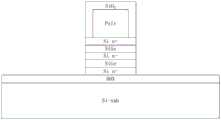
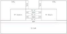
图9为本发明另一实施例环珊TFET器件的制备方法制备牺牲层和沟道层后的结构图;FIG. 9 is a structural diagram after preparing a sacrificial layer and a channel layer by a manufacturing method of a ring TFET device according to another embodiment of the present invention;
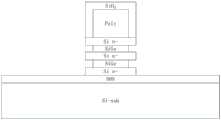
图10为本发明另一实施例环珊TFET器件的制备方法制备沟道叠层后的结构图;FIG. 10 is a structure diagram after the channel stack is prepared by the manufacturing method of the ring TFET device according to another embodiment of the present invention;
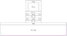
图11为本发明另一实施例环珊TFET器件的制备方法制备假栅和第一侧墙后的结构图;FIG. 11 is a structural diagram after dummy gates and first sidewalls are prepared by a manufacturing method of a surrounding TFET device according to another embodiment of the present invention;
图12为本发明另一实施例环珊TFET器件的制备方法制备内凹结构后的结构图;FIG. 12 is a structure diagram after preparing a concave structure by a method for manufacturing a ring TFET device according to another embodiment of the present invention;
图13为本发明另一实施例环珊TFET器件的制备方法制备第二侧墙后的结构图;FIG. 13 is a structural diagram after the second sidewall is prepared by the manufacturing method of the surrounding TFET device according to another embodiment of the present invention;
图14为本发明另一实施例环珊TFET器件的制备方法保护漏极的结构图;FIG. 14 is a structure diagram of a protective drain electrode of a manufacturing method of an annular TFET device according to another embodiment of the present invention;
图15为本发明另一实施例环珊TFET器件的制备方法制备源极后的结构图;15 is a structure diagram after the source is prepared by the manufacturing method of the TFET device according to another embodiment of the present invention;
图16为本发明另一实施例环珊TFET器件的制备方法保护源极的结构图;Fig. 16 is a structure diagram of protecting the source electrode of the preparation method of the TFET device according to another embodiment of the present invention;
图17为本发明另一实施例环珊TFET器件的制备方法制备漏极后的结构图;17 is a structure diagram after the drain is prepared by the manufacturing method of the TFET device according to another embodiment of the present invention;
图18为本发明另一实施例环珊TFET器件的制备方法刻蚀假栅后的结构图;FIG. 18 is a structure diagram after dummy gates are etched by a manufacturing method of a ring TFET device according to another embodiment of the present invention;
图19为本发明另一实施例环珊TFET器件的制备方法刻蚀牺牲层后的结构图;FIG. 19 is a structure diagram after etching a sacrificial layer in a manufacturing method of a ring TFET device according to another embodiment of the present invention;
图20为本发明另一实施例环珊TFET器件的制备方法制备介质金属栅后的结构图;FIG. 20 is a structure diagram after the dielectric metal gate is prepared by the manufacturing method of the surrounding TFET device according to another embodiment of the present invention;
图21为本发明另一实施例环珊TFET器件的制备方法制备金属塞后的结构图。FIG. 21 is a structure diagram after the metal plug is prepared by the manufacturing method of the surrounding TFET device according to another embodiment of the present invention.
具体实施方式Detailed ways
为使本发明实施例的目的、技术方案和优点更加清楚,下面将结合本发明实施例中的附图,对本发明实施例中的技术方案进行清楚、完整地描述,显然,所描述的实施例仅仅是本发明一部分实施例,而不是全部的实施例。基于本发明中的实施例,本领域普通技术人员在没有做出创造性劳动前提下所获得的所有其他实施例,都属于本发明保护的范围。In order to make the purpose, technical solutions and advantages of the embodiments of the present invention clearer, the technical solutions in the embodiments of the present invention will be clearly and completely described below in conjunction with the drawings in the embodiments of the present invention. Obviously, the described embodiments It is only some embodiments of the present invention, but not all embodiments. Based on the embodiments of the present invention, all other embodiments obtained by persons of ordinary skill in the art without making creative efforts belong to the protection scope of the present invention.
本发明实施例提供一种环珊TFET器件的制备方法,如图1所示,所述方法包括:The embodiment of the present invention provides a method for preparing a ring TFET device, as shown in FIG. 1, the method includes:
步骤100,在衬底上依次交替形成一个以上的沟道层和一个以上的牺牲层,以形成沟道叠层;
在一些实施例中,衬底是指承载半导体器件形成的结构。在本实施方式中,衬底例如可以采用绝缘体上硅衬底,也可以采用其他衬底。沟道层是指在形成器件后,作为沟道使用的材料膜层,牺牲层是指在制备器件的过程中会被去除的材料膜层。在本步骤中,可以采用第一层首先形成沟道层的方式,也可以采用第一层首先形成牺牲层的方式。在本实施方式中,沟道层采用轻掺杂的n型硅膜层,以满足TFET器件的沟道层要求。In some embodiments, a substrate refers to a structure on which semiconductor devices are formed. In this implementation manner, the substrate may be, for example, a silicon-on-insulator substrate, or other substrates may also be used. The channel layer refers to a material film layer used as a channel after the device is formed, and the sacrificial layer refers to a material film layer that will be removed in the process of manufacturing the device. In this step, the first layer can be used to form a channel layer first, and the first layer can also be used to form a sacrificial layer first. In this embodiment, the channel layer adopts a lightly doped n-type silicon film layer to meet the requirements of the channel layer of the TFET device.
步骤200,在衬底上形成跨所述沟道叠层的假栅,并在所述假栅的表面形成第一侧墙;
在一些实施例中,假栅是指在栅极对应的区域形成的材料膜层,该材料膜层起到占位的作用,用来为栅极预留空间位置。在后续的制备工艺中,制备栅极前,将会对假栅进行去除,去除后的形成的空间用来形成栅极。跨所述沟道叠层的假栅是指假栅的延伸方向与沟道叠层的延伸方向垂直,并且,假栅将在其自身的延伸方向上对沟道叠层的两个相对侧面进行覆盖,同时,对沟道叠层的上表面进行覆盖。对所述假栅的表面形成第一侧墙是指围绕所述假栅形成第一侧墙,第一侧墙覆盖假栅的侧表面及上表面。In some embodiments, the dummy gate refers to a material film layer formed in a region corresponding to the gate, and the material film acts as a placeholder for reserving a space for the gate. In the subsequent preparation process, before preparing the gate, the dummy gate will be removed, and the space formed after removal is used to form the gate. The dummy gate across the channel stack means that the extension direction of the dummy gate is perpendicular to the extension direction of the channel stack, and the dummy gate will conduct two opposite sides of the channel stack in its own extension direction. Covering, at the same time, covering the upper surface of the channel stack. Forming the first sidewall on the surface of the dummy gate refers to forming the first sidewall around the dummy gate, and the first sidewall covers the side surface and the upper surface of the dummy gate.
步骤300,对所述牺牲层进行刻蚀,以在所述沟道叠层的侧表面上形成内凹结构,并在所述内凹结构内形成第二侧墙;
在一些实施例中,对牺牲层进行刻蚀的过程中,由牺牲层暴露的侧壁向内刻蚀。在对所述牺牲层进行刻蚀之后,去除了部分牺牲层,在沟道叠层的侧表面对应牺牲层的位置将形成向内的凹陷。形成第二侧墙是指对内凹结构进行填充,以使沟道叠层的侧表面重新恢复平整。填充的材料可以采用SiC、Si3N4以及SiON中的其中一种或者两种以上的混合。由于牺牲层的位置是用于在后续制备环栅的,因此,第二侧墙具有两个作用,其一为限制环栅的尺寸,其二是将环栅与源漏进行绝缘。In some embodiments, during etching the sacrificial layer, the sidewalls exposed by the sacrificial layer are etched inwardly. After the sacrificial layer is etched, a part of the sacrificial layer is removed, and an inward depression is formed at a position corresponding to the sacrificial layer on the side surface of the channel stack. Forming the second sidewall refers to filling the concave structure, so that the side surface of the trench stack can be flat again. The filling material can be one of SiC, Si3 N4 and SiON or a mixture of two or more. Since the position of the sacrificial layer is used for subsequent preparation of the ring gate, the second spacer has two functions, one is to limit the size of the ring gate, and the other is to insulate the ring gate from the source and drain.
步骤400,依次制备源漏区域;在制备源极区域时,采用介质材料对漏极区域进行保护,在制备漏极区域时,采用介质材料对源极区域进行保护;
在一些实施例中,由于TFET器件的源极和漏极掺杂特性不同,因此,在制备源漏的过程中,需要对源漏分别进行制备,在制备源极时,对漏极进行覆盖保护,以免源极材料对漏极产生污染,同理,在制备漏极时,也需要对源极进行覆盖保护,以免漏极材料对源极产生污染。在制备源漏的过程中,由于沟道层的侧面是裸露的,因此,源漏将与沟道层进行接触。步骤500,对所述假栅和牺牲层进行刻蚀,以形成环栅制备空间;In some embodiments, due to the different doping characteristics of the source and drain of TFET devices, it is necessary to prepare the source and drain separately during the preparation of the source and drain, and to cover and protect the drain when preparing the source. , so as to prevent the source material from polluting the drain. Similarly, when preparing the drain, the source also needs to be covered and protected to prevent the drain material from polluting the source. In the process of preparing the source and drain, since the side of the channel layer is exposed, the source and drain will be in contact with the channel layer.
在一些实施例中,由于假栅和牺牲层占据了环栅的空间,因此,在制备环栅之前,需要对假栅和牺牲层进行去除,在去除的过程中,由于假栅和牺牲层具有不同的刻蚀特性,因此可以采用分次刻蚀的方式进行去除。In some embodiments, since the dummy gate and the sacrificial layer occupy the space of the ring gate, it is necessary to remove the dummy gate and the sacrificial layer before preparing the ring ring. During the removal process, the dummy gate and the sacrificial layer have Different etching characteristics, so it can be removed by etching in stages.
步骤600,在所述环栅制备空间内制备环形的介质金属栅,以形成环栅TFET器件。
在一些实施例中,由于牺牲层和假栅去除后,牺牲层和假栅所占的空间形成了空腔,为环栅的制备提供了空间。由于假栅和牺牲层对沟道层形成了包裹的结构,因此,空腔也是环绕沟道层形成的,在空腔中形成介质金属后,介质金属会环绕沟道层形成环栅。在一些实施例中,介质层可以选用高K材料如HfO2,ZrO2,Al2O3等。In some embodiments, after the sacrificial layer and the dummy gate are removed, a cavity is formed in the space occupied by the sacrificial layer and the dummy gate, which provides space for the preparation of the ring gate. Since the dummy gate and the sacrificial layer form a wrapping structure for the channel layer, the cavity is also formed around the channel layer. After the dielectric metal is formed in the cavity, the dielectric metal will surround the channel layer to form a ring gate. In some embodiments, the dielectric layer can be made of high-K materials such as HfO2 , ZrO2 , Al2 O3 and so on.
在发明实施例提供的技术方案中,通过沟道叠层的设置,将假栅与牺牲层进行配合,提供了TFET器件的前期结构,在制备源漏区域时,通过对源漏的依次制备,并在制备源极时对漏极进行覆盖保护,在制备漏极时对源极进行覆盖保护,实现了TFET器件的源漏制备,最后通过对假栅以及牺牲层的去除和介质金属栅的制备,为源漏之间的沟道层提供了环栅。通过本发明提供的技术方案,能够将TFET器件与环栅器件的生产工艺相兼容,实现环栅TFET器件的批量生产,有效的提高了生产效率。In the technical solution provided by the embodiment of the invention, through the arrangement of the channel stack, the dummy gate and the sacrificial layer are combined to provide the early structure of the TFET device. When preparing the source and drain regions, the source and drain are sequentially prepared, And the drain is covered and protected when the source is prepared, and the source is covered and protected when the drain is prepared, realizing the preparation of the source and drain of the TFET device, and finally through the removal of the dummy gate and the sacrificial layer and the preparation of the dielectric metal gate , providing a gate-around for the channel layer between source and drain. Through the technical solution provided by the invention, the production process of the TFET device and the gate-around device can be compatible, and the mass production of the gate-around TFET device can be realized, thereby effectively improving the production efficiency.
作为一种可选的实施方式,如图2所示,在衬底上依次交替形成一个以上的沟道层和一个以上的牺牲层,以形成沟道叠层包括:As an optional implementation manner, as shown in FIG. 2, forming more than one channel layer and more than one sacrificial layer alternately on the substrate in sequence to form a channel stack includes:
步骤110,在绝缘体上硅衬底上采用外延的方式交替形成硅锗膜层和硼掺杂的硅膜层,其中,硅锗膜层为牺牲层,硼掺杂的硅膜层为沟道层;
在一些实施例中,硅膜层具备沟道层的特性,可以用来作为沟道层使用,而硅锗膜层则在刻蚀过程中能够与硅膜层表现出选择比,更有利于在刻蚀过程中将硅锗膜层刻蚀,而将硅膜层保留。In some embodiments, the silicon film layer has the characteristics of a channel layer and can be used as a channel layer, while the silicon germanium film layer can show a selectivity ratio with the silicon film layer during the etching process, which is more conducive to During the etching process, the silicon germanium film layer is etched while the silicon film layer remains.
步骤120,采用干法刻蚀工艺对所述沟道叠层进行刻蚀,以形成沿第一方向延伸的鳍片形状的沟道叠层。
在一些实施例中,由于在外延生长的过程中,会在衬底的整个表面上形成沟道叠层,为了实现器件的制备,需要对沟道叠层进行刻蚀形成鳍片形状。鳍片形状的沟道叠层有利于在形成跨沟道叠层的假栅形成。In some embodiments, since the channel stack is formed on the entire surface of the substrate during the epitaxial growth process, the channel stack needs to be etched to form a fin shape in order to realize the fabrication of the device. The fin-shaped channel stack facilitates dummy gate formation when forming across the channel stack.
作为一种可选的实施方式,如图3所示,在衬底上形成跨所述沟道叠层的假栅包括:As an optional implementation manner, as shown in FIG. 3 , forming a dummy gate across the channel stack on the substrate includes:
步骤210,在所述衬底表面和所述沟道叠层上形成第一膜层;
在一些实施例中,在形成第一膜层时,会对衬底和沟道叠层上形成覆盖,并且,会形成由衬底表面到沟道叠层表面的随形结构,从而,将沟道叠层的侧壁进行覆盖。In some embodiments, when the first film layer is formed, the substrate and the channel stack will be covered, and a conformal structure will be formed from the substrate surface to the channel stack surface, so that the trench The sidewall of the channel stack is covered.
步骤220,依据所述沟道叠层的图案形状,对所述第一膜层进行刻蚀,以形成沿第一方向与所述沟道叠层具有台阶,沿第二方向跨过所述沟道叠层的假栅。Step 220: Etching the first film layer according to the pattern shape of the channel stack to form a step along the first direction with the channel stack and across the trench along the second direction. The dummy gate of the channel stack.
在一些实施例中,在对第一膜层进行刻蚀时,保留的部分在第一方向上的尺寸小于所述沟道叠层在第一方向上的尺寸,从而,形成由沟道叠层到第一膜层的台阶;保留的部分在第二方向上的尺寸大于所述沟道叠层在第二方向上的尺寸,从而,形成跨沟道叠层的假栅。假栅在第一方向的轴线与沟道叠层在第一方向的轴线对齐,假栅在第二方向的轴线与沟道叠层在第二方向轴线对齐。In some embodiments, when the first film layer is etched, the size of the remaining portion in the first direction is smaller than the size of the channel stack in the first direction, so that the channel stack formed by The step to the first film layer; the remaining portion has a dimension in the second direction greater than the dimension of the channel stack in the second direction, thereby forming a dummy gate across the channel stack. The axis of the dummy gate in the first direction is aligned with the axis of the channel stack in the first direction, and the axis of the dummy gate in the second direction is aligned with the axis of the channel stack in the second direction.
作为一种可选的实施方式,如图4所示,在所述假栅的表面形成第一侧墙包括:As an optional implementation manner, as shown in FIG. 4 , forming the first sidewall on the surface of the dummy gate includes:
步骤230,在所述假栅、沟道叠层以及衬底表面形成第二膜层,其中,所述第二膜层与所述第一膜层具有刻蚀选择比;
在一些实施例中,第二膜层在形成的过程中,会对假栅、沟道叠层以及衬底表面覆盖并形成随形结构,从而,会对假栅以及沟道叠层的侧面也形成覆盖。第二膜层与第一膜层具有刻蚀选择比,能够在刻蚀假栅的过程中不损伤第二膜层,即,不损坏第一侧墙,有利于后续的环栅形成。In some embodiments, during the formation process, the second film layer will cover the dummy gate, the channel stack and the surface of the substrate and form a conformal structure, so that the side surfaces of the dummy gate and the channel stack will also be covered. Form a cover. The second film layer has an etching selectivity ratio to the first film layer, so that the second film layer can not be damaged during the process of etching the dummy gate, that is, the first spacer can not be damaged, which is beneficial to the subsequent formation of the ring gate.
步骤240,对所述第二膜层进行刻蚀,以形成沿第一方向与所述沟道叠层侧表面对齐,围绕所述假栅侧表面并覆盖所述假栅上表面的第一侧墙。
在一些实施例中,在对第二膜层进行刻蚀时,保留的部分在第一方向上与沟道叠层的侧表面对齐,从而,能够将沟道叠层的侧面进行暴露,这样才能够在后续对牺牲层进行刻蚀形成内凹结构。并且,由于假栅在第一方向上的尺寸小于沟道叠层在第一方向上的尺寸,在刻蚀完成后,在假栅垂直于第一方向的两个侧面具有足够的厚度形成侧墙。In some embodiments, when the second film layer is etched, the remaining portion is aligned with the side surface of the channel stack in the first direction, so that the side surface of the channel stack can be exposed, so that The sacrificial layer can be subsequently etched to form a recessed structure. Moreover, since the size of the dummy gate in the first direction is smaller than the size of the channel stack in the first direction, after the etching is completed, the two sides of the dummy gate perpendicular to the first direction have sufficient thickness to form sidewalls .
作为一种可选的实施方式,对所述牺牲层进行刻蚀,以在所述沟道叠层的侧表面上形成内凹结构包括:As an optional implementation manner, etching the sacrificial layer to form a concave structure on a side surface of the channel stack includes:
对所述牺牲层暴露的侧壁向内进行刻蚀,以形成内凹结构;其中,刻蚀深度与所述第一侧墙的厚度相等。The exposed sidewall of the sacrificial layer is etched inward to form a concave structure; wherein the etching depth is equal to the thickness of the first sidewall.
在一些实施例中,由于环栅在形成的过程中,是占用了假栅以及牺牲层的空间形成的,因此,在本实施方式中,将刻蚀深度设置为与第一侧墙的厚度相等,有助于形成在第一方向上尺寸一致的环栅。In some embodiments, since the gate ring is formed by occupying the space of the dummy gate and the sacrificial layer during the formation process, in this embodiment, the etching depth is set to be equal to the thickness of the first sidewall , which helps to form a ring gate with uniform dimensions in the first direction.
作为一种可选的实施方式,如图5所示,在所述内凹结构内形成第二侧墙包括:As an optional implementation manner, as shown in FIG. 5 , forming the second side wall in the concave structure includes:
步骤310,形成第三膜层,所述第三膜层的厚度不小于所述内凹结构的深度;
在一些实施例中,在形成第三膜层的过程中,随着对各个部分的上表面的覆盖以及随形结构的形成,将对整个器件的表面进行覆盖。为了将内凹结构填满,将第三膜层的厚度设置为不小于内凹结构的深度。In some embodiments, during the process of forming the third film layer, along with the covering of the upper surface of each part and the formation of the conformal structure, the entire surface of the device will be covered. In order to fill up the concave structure, the thickness of the third film layer is set to be not less than the depth of the concave structure.
步骤320,对所述第三膜层进行刻蚀,以形成在第一方向上与所述沟道层对齐的第二侧墙。
在一些实施例中,对第三膜层进行刻蚀的过程中,会将内凹结构之外的部分全部刻蚀去掉,仅保留内凹结构内的部分作为第二侧墙。In some embodiments, during the etching process of the third film layer, all the parts outside the concave structure are etched away, and only the part inside the concave structure remains as the second sidewall.
作为一种可选的实施方式,如图6所示,在制备源极区域时,采用介质材料对漏极区域进行保护:As an optional implementation, as shown in FIG. 6, when preparing the source region, the drain region is protected by a dielectric material:
步骤410,形成第二膜层;
在一些实施例中,由于在形成第二膜层时,会将源极、漏极以及假栅全部覆盖。In some embodiments, the source, the drain and the dummy gate are all covered when the second film layer is formed.
步骤420,对所述第二膜层进行刻蚀,以使所述源极区域对应的衬底上表面暴露;
在一些实施例中,为了制备源极,需要将第二膜层进行刻蚀,使衬底上表面暴露出来,这样才能够使源极与沟道层进行接触。在刻蚀的过程中,可以仅刻蚀源极制备所需要的区域,也可以将漏极之外的区域的第二膜层全部刻蚀去除。In some embodiments, in order to prepare the source electrode, the second film layer needs to be etched to expose the upper surface of the substrate, so that the source electrode can be in contact with the channel layer. During the etching process, only the region required for the preparation of the source electrode may be etched, or all the second film layer in the region other than the drain electrode may be etched away.
步骤430,在所述衬底暴露的上表面采用原位掺杂的方式外延形成源极;
在一些实施例中,在衬底暴露以后,沟道层的侧壁也会暴露出来,此时,在衬底上进行源极的制备,能够使源极与沟道进行接触。In some embodiments, after the substrate is exposed, the sidewall of the channel layer is also exposed. At this time, the source electrode is prepared on the substrate, so that the source electrode can be in contact with the channel.
步骤440,对所述漏极区域对应的第二膜层进行去除。
在一些实施例总,在源极制备完成以后,由于后续还需要制备漏极,因此,需要将漏极的第二膜层进行去除。当然,由于后续的漏极制备过程中还会再次沉积第二膜层,也可以在源极制备完成后部去除漏极区域对应的第二膜层,而在漏极制备过程中,形成对源极的保护膜层之后一并进行漏极区域的第二膜层的去除。In some embodiments, after the preparation of the source electrode is completed, since the drain electrode needs to be prepared later, the second film layer of the drain electrode needs to be removed. Of course, since the second film layer will be deposited again in the subsequent drain preparation process, the second film layer corresponding to the drain region can also be removed after the source preparation is completed, and in the drain preparation process, the formation of the opposite source After that, remove the second film layer in the drain region.
作为一种可选的实施方式,如图7所示,在制备漏极区域时,采用介质材料对源极区域进行保护包括:As an optional implementation manner, as shown in FIG. 7, when preparing the drain region, using a dielectric material to protect the source region includes:
步骤450,形成第二膜层;
在一些实施例中,由于在形成第二膜层时,会将源极、漏极以及假栅全部覆盖。In some embodiments, the source, the drain and the dummy gate are all covered when the second film layer is formed.
步骤460,对所述第二膜层进行刻蚀,以使所述漏极区域对应的衬底上表面暴露;
在一些实施例中,为了制备漏极,需要将第二膜层进行刻蚀,使衬底上表面暴露出来,这样才能够使漏极与沟道层进行接触。在刻蚀的过程中,可以仅刻蚀漏极制备所需要的区域,也可以将漏极之外的区域的第二膜层全部刻蚀去除。In some embodiments, in order to prepare the drain, the second film layer needs to be etched to expose the upper surface of the substrate, so that the drain can be in contact with the channel layer. During the etching process, only the area required for the preparation of the drain may be etched, or all the second film layer in the area other than the drain may be etched away.
步骤470,在所述衬底暴露的上表面采用原位掺杂的方式外延形成漏极;
在一些实施例中,在衬底暴露以后,沟道层的侧壁也会暴露出来,此时,在衬底上进行漏极的制备,能够使漏极与沟道进行接触。In some embodiments, after the substrate is exposed, the sidewall of the channel layer is also exposed. At this time, the drain is prepared on the substrate, so that the drain can be in contact with the channel.
步骤480,对所述源极区域的第二膜层进行去除。
在一些实施例中,在漏极制备完成后,由于第二膜层是对源极进行保护的,因此,第二膜层通常会被污染,因此,会对其进行去除,以避免由于污染导致的器件性能下降。当然,当漏极制备的过程中,如果对第二膜层的污染程度在可接受范围之内,也可以对其进行保留,以减少后续膜层填充时的用量。In some embodiments, after the preparation of the drain electrode is completed, since the second film layer is used to protect the source electrode, the second film layer will usually be polluted, so it will be removed to avoid contamination due to pollution. device performance degrades. Of course, during the preparation of the drain electrode, if the pollution degree of the second film layer is within an acceptable range, it can also be retained, so as to reduce the amount used when filling the subsequent film layer.
作为一种可选的实施方式,如图8所示,对所述假栅和牺牲层进行刻蚀,以形成环栅制备空间包括:As an optional implementation manner, as shown in FIG. 8 , etching the dummy gate and the sacrificial layer to form a ring gate preparation space includes:
步骤510,对器件进行平坦化,以去除假栅顶部的第二膜层,暴露所述假栅的上表面;
在一些实施例中,由于在对第二膜层在形成时,覆盖了假栅的顶部,在刻蚀的过程中,假栅顶部的部分也至少有部分被保留下来,在对假栅进行刻蚀之前,需要首先对顶部覆盖的第二膜层进行平坦化,将假栅暴露出来之后,才能够进行刻蚀。In some embodiments, since the top of the dummy gate is covered when the second film layer is formed, during the etching process, at least part of the top of the dummy gate is also retained. Before etching, it is necessary to first planarize the second film layer covering the top, and only after exposing the dummy gate can etching be performed.
步骤520,对所述假栅进行湿法刻蚀,以去除所述假栅,暴露所述牺牲层;
在一些实施例中,由于假栅与第一侧墙和牺牲层均具有不同的刻蚀特性,因此,采用湿法刻蚀能够在刻蚀过程中仅将假栅刻蚀去除,而不会影响第一侧墙和牺牲层。In some embodiments, since the dummy gate has different etching characteristics from the first sidewall and the sacrificial layer, only the dummy gate can be etched and removed during the etching process by using wet etching without affecting First side wall and sacrificial layer.
步骤530,对所述牺牲层进行化学刻蚀或者原子层刻蚀,以去除所述牺牲层,形成环栅所需的空间。
在一些实施例中,由于牺牲层处于环绕沟道层的空间内,其结构存在被遮挡的部分,为了顺利的刻蚀牺牲层,需要采用化学刻蚀或者原子层刻蚀。In some embodiments, since the sacrificial layer is located in the space surrounding the channel layer, its structure has a shielded part. In order to etch the sacrificial layer smoothly, chemical etching or atomic layer etching is required.
作为一种可选的实施方式,在所述环栅制备空间内制备环形的介质金属栅,以形成环栅TFET器件包括:As an optional implementation manner, preparing a ring-shaped dielectric metal gate in the ring-gate preparation space to form a ring-gate TFET device includes:
采用原子层沉积或者气相沉积的方式,所述环形栅制备空间内形成环形的介质金属栅。By means of atomic layer deposition or vapor deposition, a ring-shaped dielectric metal grid is formed in the ring-shaped gate preparation space.
在一些实施例中,由于环栅制备空间是一个环绕沟道层形成的异形空间,为了实现在该空间内制备介质金属栅,需要采用原子层沉积或者气相沉积的方式来实现。In some embodiments, since the ring gate preparation space is a special-shaped space formed around the channel layer, in order to realize the fabrication of the dielectric metal gate in this space, atomic layer deposition or vapor deposition is required.
如图9-18所示,提供了一种示例性的实施方式,对本发明提供的技术方案予以说明:As shown in Figures 9-18, an exemplary implementation is provided to describe the technical solution provided by the present invention:
首先,在SOI(Silicon On Insulator,绝缘层上的硅)片上通过外延方式依次生长SiGe,掺杂硼的Si层;其中,掺杂硼的Si层决定了后续纳米线根数;掺杂硼的Si层至少为一层。在本实施方式中,SiGe层为牺牲层,掺杂硼的Si层为沟道层。形成叠层之后,其结构如图9所示。为了将叠层的形状制备为符合器件要求的形状,需要对叠层进行光刻和刻蚀,刻蚀的方式例如可以采用干法刻蚀。刻蚀完成后,形成沟道叠层,其结构如图10所示。通过沉积膜层,例如多晶硅膜层,以及对多晶硅膜层的刻蚀,形成假栅。再次沉积膜层,例如二氧化硅膜层,以及对二氧化硅膜层的刻蚀,形成第一侧墙,形成第一侧墙后的结构如图11所示。在形成第一侧墙之后,对牺牲层进行刻蚀,形成向内的凹陷结构,如图12所示。在形成凹陷结构之后,通过沉积膜层,例如氮化硅膜层,以及对氮化硅膜层的刻蚀,形成第二侧墙,形成第二侧墙之后的结构如图13所示。在侧墙的形成过程中,可以采用高选择比的各向异性刻蚀方式进行刻蚀,在刻蚀的过程中,水平平面上的膜层会被快速刻蚀掉,而竖直平面上的膜层将以较慢的速率被刻蚀掉。在形成第二侧墙之后,对器件进行介质填充,例如可以采用二氧化硅进行填充,填充完成后,对介质进行光刻刻蚀,暴露出源极区域,其结构如图14所示。在暴露出源极区域之后,在源极区域通过原位掺杂方式外延掺杂B离子的SiGe,形成源极,其结构如图15所示。采用与源极的形成方式类似的方式,对器件进行介质填充后,对漏极区域进行光刻刻蚀,暴露出漏极区域,其结构如图16所示。在暴露出漏极区域之后,在漏极区域通过原位掺杂方式外延SiGe-P形成漏极,其结构如图17所示。在形成漏极后,对源极区域的介质进行去除,其结构如图18所示。在形成源漏之后,对器件进行介质填充并平坦化,例如采用化学机械研磨的方式进行平坦化,打开假栅顶部的二氧化硅膜层。再采用刻蚀的方式对假栅进行去除,例如可以采用湿法刻蚀的方式对假栅进行去除。去除假栅后的结构如图18所示。在完成上述的步骤之后,牺牲层被暴露出来,此时可以对牺牲层进行刻蚀,刻蚀方式例如可以为干法刻蚀、湿法原子层刻蚀或者氯化氢气体反应的方式进行刻蚀。刻蚀完成后,假栅和牺牲层所占用的空间形成空腔,其结构如图19所示。再在假栅和牺牲层所在空间内生长高K介质金属栅,即形成环形介质金属栅,其结构如图20所示。完成上述的步骤之后,再形成膜层,例如二氧化硅介质膜层,对介质膜层开孔再形成金属塞,即可形成最终的器件。器件结构如图21所示。First, on the SOI (Silicon On Insulator, silicon on insulating layer) wafer, SiGe and boron-doped Si layers are grown sequentially by epitaxy; among them, the boron-doped Si layer determines the number of subsequent nanowires; the boron-doped Si layer determines the number of subsequent nanowires; The Si layer is at least one layer. In this embodiment, the SiGe layer is a sacrificial layer, and the boron-doped Si layer is a channel layer. After the stack is formed, its structure is shown in FIG. 9 . In order to prepare the shape of the laminate into a shape required by the device, it is necessary to perform photolithography and etching on the laminate, and the etching method may be, for example, dry etching. After the etching is completed, a channel stack is formed, the structure of which is shown in FIG. 10 . The dummy gate is formed by depositing a film layer, such as a polysilicon film layer, and etching the polysilicon film layer. A film layer, such as a silicon dioxide film layer, is deposited again, and the silicon dioxide film layer is etched to form a first side wall. The structure after forming the first side wall is shown in FIG. 11 . After forming the first sidewall, the sacrificial layer is etched to form an inward recessed structure, as shown in FIG. 12 . After the concave structure is formed, a second side wall is formed by depositing a film layer, such as a silicon nitride film layer, and etching the silicon nitride film layer. The structure after forming the second side wall is shown in FIG. 13 . In the formation process of the side wall, anisotropic etching method with high selectivity can be used for etching. During the etching process, the film layer on the horizontal plane will be quickly etched away, while the film layer on the vertical plane The film layer will be etched away at a slower rate. After forming the second sidewall, the device is filled with a dielectric, for example, silicon dioxide can be used for filling. After the filling is completed, the dielectric is etched by photolithography to expose the source region, and its structure is shown in FIG. 14 . After the source region is exposed, SiGe doped with B ions is epitaxially doped in the source region by in-situ doping to form the source, the structure of which is shown in FIG. 15 . In a manner similar to that of the source electrode, after the device is filled with a dielectric, the drain region is photolithographically etched to expose the drain region, and its structure is shown in FIG. 16 . After the drain region is exposed, epitaxial SiGe-P is formed in the drain region by in-situ doping to form the drain, and its structure is shown in FIG. 17 . After the drain is formed, the dielectric in the source region is removed, and its structure is shown in FIG. 18 . After the source and drain are formed, the device is filled with a dielectric and planarized, for example, by means of chemical mechanical polishing, to open the silicon dioxide film layer on the top of the dummy gate. The dummy gate is then removed by etching, for example, the dummy gate may be removed by wet etching. The structure after removing the dummy gate is shown in Figure 18. After the above steps are completed, the sacrificial layer is exposed. At this time, the sacrificial layer can be etched. The etching method can be, for example, dry etching, wet atomic layer etching or hydrogen chloride gas reaction. After the etching is completed, the space occupied by the dummy gate and the sacrificial layer forms a cavity, the structure of which is shown in FIG. 19 . Then, a high-K dielectric metal gate is grown in the space where the dummy gate and the sacrificial layer are located, that is, a ring-shaped dielectric metal gate is formed, and its structure is shown in FIG. 20 . After the above-mentioned steps are completed, a film layer, such as a silicon dioxide dielectric film layer, is formed, holes are opened in the dielectric film layer, and metal plugs are formed to form the final device. The device structure is shown in Figure 21.
以上所述,仅为本发明的具体实施方式,但本发明的保护范围并不局限于此,任何熟悉本技术领域的技术人员在本发明揭露的技术范围内,可轻易想到的变化或替换,都应涵盖在本发明的保护范围之内。因此,本发明的保护范围应该以权利要求的保护范围为准。The above is only a specific embodiment of the present invention, but the scope of protection of the present invention is not limited thereto. Anyone skilled in the art can easily think of changes or substitutions within the technical scope disclosed in the present invention. All should be covered within the protection scope of the present invention. Therefore, the protection scope of the present invention should be determined by the protection scope of the claims.
Claims (10)
Priority Applications (3)
| Application Number | Priority Date | Filing Date | Title |
|---|---|---|---|
| CN202211533675.3ACN116072542A (en) | 2022-11-30 | 2022-11-30 | Preparation method of ring grid TFET device |
| US18/708,028US20250006822A1 (en) | 2022-11-30 | 2023-11-27 | Method for manufacturing gate-all-around tfet device |
| PCT/CN2023/134341WO2024114579A1 (en) | 2022-11-30 | 2023-11-27 | Method for preparing gate-all-around tfet device |
Applications Claiming Priority (1)
| Application Number | Priority Date | Filing Date | Title |
|---|---|---|---|
| CN202211533675.3ACN116072542A (en) | 2022-11-30 | 2022-11-30 | Preparation method of ring grid TFET device |
Publications (1)
| Publication Number | Publication Date |
|---|---|
| CN116072542Atrue CN116072542A (en) | 2023-05-05 |
Family
ID=86169066
Family Applications (1)
| Application Number | Title | Priority Date | Filing Date |
|---|---|---|---|
| CN202211533675.3APendingCN116072542A (en) | 2022-11-30 | 2022-11-30 | Preparation method of ring grid TFET device |
Country Status (3)
| Country | Link |
|---|---|
| US (1) | US20250006822A1 (en) |
| CN (1) | CN116072542A (en) |
| WO (1) | WO2024114579A1 (en) |
Cited By (2)
| Publication number | Priority date | Publication date | Assignee | Title |
|---|---|---|---|---|
| WO2024114579A1 (en)* | 2022-11-30 | 2024-06-06 | 中国科学院微电子研究所 | Method for preparing gate-all-around tfet device |
| CN120417421A (en)* | 2025-04-24 | 2025-08-01 | 北京集成电路装备创新中心有限公司 | A method for preparing a gate-all-around transistor device and a gate-all-around transistor device |
Family Cites Families (7)
| Publication number | Priority date | Publication date | Assignee | Title |
|---|---|---|---|---|
| US9647098B2 (en)* | 2014-07-21 | 2017-05-09 | Samsung Electronics Co., Ltd. | Thermionically-overdriven tunnel FETs and methods of fabricating the same |
| US9660027B2 (en)* | 2015-10-20 | 2017-05-23 | Globalfoundries Inc. | Expitaxially regrown heterostructure nanowire lateral tunnel field effect transistor |
| CN111370489A (en)* | 2016-11-21 | 2020-07-03 | 华为技术有限公司 | Field effect transistor and manufacturing method thereof |
| US11335807B2 (en)* | 2018-06-29 | 2022-05-17 | Intel Corporation | Isolation schemes for gate-all-around transistor devices |
| CN113178489B (en)* | 2021-03-03 | 2024-04-02 | 中国科学院微电子研究所 | A Z2-FET device and a method for preparing the same, and a semiconductor device |
| KR102459732B1 (en)* | 2021-05-13 | 2022-10-27 | (재)한국나노기술원 | Manufacturing method of semiconductor device with gate-all-around channel |
| CN116072542A (en)* | 2022-11-30 | 2023-05-05 | 中国科学院微电子研究所 | Preparation method of ring grid TFET device |
- 2022
- 2022-11-30CNCN202211533675.3Apatent/CN116072542A/enactivePending
- 2023
- 2023-11-27USUS18/708,028patent/US20250006822A1/enactivePending
- 2023-11-27WOPCT/CN2023/134341patent/WO2024114579A1/ennot_activeCeased
Cited By (2)
| Publication number | Priority date | Publication date | Assignee | Title |
|---|---|---|---|---|
| WO2024114579A1 (en)* | 2022-11-30 | 2024-06-06 | 中国科学院微电子研究所 | Method for preparing gate-all-around tfet device |
| CN120417421A (en)* | 2025-04-24 | 2025-08-01 | 北京集成电路装备创新中心有限公司 | A method for preparing a gate-all-around transistor device and a gate-all-around transistor device |
Also Published As
| Publication number | Publication date |
|---|---|
| US20250006822A1 (en) | 2025-01-02 |
| WO2024114579A1 (en) | 2024-06-06 |
Similar Documents
| Publication | Publication Date | Title |
|---|---|---|
| CN104576735B (en) | FinFET with buried insulator layer and forming method thereof | |
| TWI785126B (en) | Semiconductor device structure and method for forming the same | |
| CN111223779B (en) | Semiconductor structure and forming method thereof | |
| US20090239346A1 (en) | Semiconductor device with finfet and method of fabricating the same | |
| CN101369598A (en) | semiconductor structure | |
| CN111223778B (en) | Semiconductor structure and forming method thereof | |
| CN105280496A (en) | Semiconductor element with fin structure and manufacturing method thereof | |
| KR102807518B1 (en) | Nanowire/sheet devices having self-aligning isolation regions, methods for fabricating them, and electronic devices | |
| US20250006822A1 (en) | Method for manufacturing gate-all-around tfet device | |
| TW201806158A (en) | Fin field effect transistor positioned on the insulating layer and forming method thereof | |
| CN115360145A (en) | A kind of semiconductor structure and its manufacturing method | |
| CN102254948A (en) | Tunneling field effect transistor with double-gate structure and preparing method thereof | |
| CN111477684B (en) | Semiconductor device having U-shaped structure, method of manufacturing the same, and electronic apparatus | |
| CN113130311B (en) | Semiconductor structure and forming method thereof | |
| CN104167393A (en) | Semiconductor device manufacturing method | |
| CN114068706B (en) | Semiconductor structure and forming method thereof | |
| CN111063728B (en) | C-shaped active region semiconductor device, method of manufacturing the same, and electronic apparatus including the same | |
| CN110854194B (en) | Semiconductor structure and forming method thereof | |
| CN104103506B (en) | Semiconductor device manufacturing method | |
| CN117476466A (en) | Preparation methods, semiconductor structures, devices and electronic equipment for bottom dielectric isolation | |
| CN103632978B (en) | The forming method of semiconductor structure | |
| CN115763539A (en) | Method for eliminating damage of ring gate nanosheet channel | |
| CN117116854A (en) | Semiconductor structures and methods of forming them | |
| CN110224029B (en) | Semiconductor device, manufacturing method thereof and electronic equipment comprising semiconductor device | |
| US10651092B2 (en) | Semiconductor device and fabrication method thereof |
Legal Events
| Date | Code | Title | Description |
|---|---|---|---|
| PB01 | Publication | ||
| PB01 | Publication | ||
| SE01 | Entry into force of request for substantive examination | ||
| SE01 | Entry into force of request for substantive examination |