CN116060148A - A method for in-situ controllable hydrophobic modification of nanochannels - Google Patents
A method for in-situ controllable hydrophobic modification of nanochannelsDownload PDFInfo
- Publication number
- CN116060148A CN116060148ACN202310129050.9ACN202310129050ACN116060148ACN 116060148 ACN116060148 ACN 116060148ACN 202310129050 ACN202310129050 ACN 202310129050ACN 116060148 ACN116060148 ACN 116060148A
- Authority
- CN
- China
- Prior art keywords
- chip
- channel
- deionized water
- hydrophobic modification
- solution
- Prior art date
- Legal status (The legal status is an assumption and is not a legal conclusion. Google has not performed a legal analysis and makes no representation as to the accuracy of the status listed.)
- Granted
Links
- 239000002090nanochannelSubstances0.000titleclaimsabstractdescription54
- 230000002209hydrophobic effectEffects0.000titleclaimsabstractdescription46
- 230000004048modificationEffects0.000titleclaimsabstractdescription43
- 238000012986modificationMethods0.000titleclaimsabstractdescription43
- 238000000034methodMethods0.000titleclaimsabstractdescription33
- 238000011065in-situ storageMethods0.000titleclaimsabstractdescription19
- XLYOFNOQVPJJNP-UHFFFAOYSA-NwaterChemical compoundOXLYOFNOQVPJJNP-UHFFFAOYSA-N0.000claimsabstractdescription54
- 239000000243solutionSubstances0.000claimsabstractdescription46
- 239000008367deionised waterSubstances0.000claimsabstractdescription27
- 229910021641deionized waterInorganic materials0.000claimsabstractdescription27
- 238000002474experimental methodMethods0.000claimsabstractdescription23
- 239000003607modifierSubstances0.000claimsabstractdescription22
- 238000002347injectionMethods0.000claimsabstractdescription20
- 239000007924injectionSubstances0.000claimsabstractdescription20
- 230000008569processEffects0.000claimsabstractdescription18
- CSCPPACGZOOCGX-UHFFFAOYSA-NAcetoneChemical compoundCC(C)=OCSCPPACGZOOCGX-UHFFFAOYSA-N0.000claimsabstractdescription16
- LFQSCWFLJHTTHZ-UHFFFAOYSA-NEthanolChemical compoundCCOLFQSCWFLJHTTHZ-UHFFFAOYSA-N0.000claimsabstractdescription16
- 238000004506ultrasonic cleaningMethods0.000claimsabstractdescription11
- 241000252506CharaciformesSpecies0.000claimsabstractdescription9
- 238000002715modification methodMethods0.000claimsabstractdescription6
- 238000010438heat treatmentMethods0.000claimsabstractdescription4
- 238000003760magnetic stirringMethods0.000claimsabstractdescription4
- 238000009210therapy by ultrasoundMethods0.000claimsabstractdescription3
- 238000005406washingMethods0.000claimsabstractdescription3
- IJGRMHOSHXDMSA-UHFFFAOYSA-NAtomic nitrogenChemical compoundN#NIJGRMHOSHXDMSA-UHFFFAOYSA-N0.000claimsdescription42
- 229910052757nitrogenInorganic materials0.000claimsdescription21
- IJOOHPMOJXWVHK-UHFFFAOYSA-NchlorotrimethylsilaneChemical compoundC[Si](C)(C)ClIJOOHPMOJXWVHK-UHFFFAOYSA-N0.000claimsdescription12
- VYPSYNLAJGMNEJ-UHFFFAOYSA-NSilicium dioxideChemical compoundO=[Si]=OVYPSYNLAJGMNEJ-UHFFFAOYSA-N0.000claimsdescription9
- 238000012360testing methodMethods0.000claimsdescription7
- YXFVVABEGXRONW-UHFFFAOYSA-NTolueneChemical compoundCC1=CC=CC=C1YXFVVABEGXRONW-UHFFFAOYSA-N0.000claimsdescription6
- VLKZOEOYAKHREP-UHFFFAOYSA-Nn-HexaneChemical compoundCCCCCCVLKZOEOYAKHREP-UHFFFAOYSA-N0.000claimsdescription6
- 239000005051trimethylchlorosilaneSubstances0.000claimsdescription6
- 239000005046ChlorosilaneSubstances0.000claimsdescription4
- KOPOQZFJUQMUML-UHFFFAOYSA-NchlorosilaneChemical compoundCl[SiH3]KOPOQZFJUQMUML-UHFFFAOYSA-N0.000claimsdescription4
- 235000012239silicon dioxideNutrition0.000claimsdescription4
- 239000000377silicon dioxideSubstances0.000claimsdescription4
- 238000001035dryingMethods0.000claimsdescription2
- -1octadecyl trimethylsilane ChlorosilanesChemical class0.000claimsdescription2
- 238000004140cleaningMethods0.000abstractdescription4
- 239000011148porous materialSubstances0.000description8
- XUIMIQQOPSSXEZ-UHFFFAOYSA-NSiliconChemical compound[Si]XUIMIQQOPSSXEZ-UHFFFAOYSA-N0.000description7
- 239000003079shale oilSubstances0.000description7
- 239000010703siliconSubstances0.000description7
- 238000005516engineering processMethods0.000description6
- 239000007789gasSubstances0.000description6
- 239000011159matrix materialSubstances0.000description6
- 229910052710siliconInorganic materials0.000description6
- 230000005499meniscusEffects0.000description4
- VNWKTOKETHGBQD-UHFFFAOYSA-NmethaneChemical compoundCVNWKTOKETHGBQD-UHFFFAOYSA-N0.000description4
- 230000008859changeEffects0.000description3
- 238000011161developmentMethods0.000description3
- 239000012530fluidSubstances0.000description3
- WYTZZXDRDKSJID-UHFFFAOYSA-N(3-aminopropyl)triethoxysilaneChemical compoundCCO[Si](OCC)(OCC)CCCNWYTZZXDRDKSJID-UHFFFAOYSA-N0.000description2
- GRYLNZFGIOXLOG-UHFFFAOYSA-NNitric acidChemical compoundO[N+]([O-])=OGRYLNZFGIOXLOG-UHFFFAOYSA-N0.000description2
- 230000015572biosynthetic processEffects0.000description2
- 238000006243chemical reactionMethods0.000description2
- 239000010779crude oilSubstances0.000description2
- 238000010586diagramMethods0.000description2
- 239000011521glassSubstances0.000description2
- 239000000463materialSubstances0.000description2
- 238000000520microinjectionMethods0.000description2
- 239000003345natural gasSubstances0.000description2
- 229910017604nitric acidInorganic materials0.000description2
- 238000012545processingMethods0.000description2
- 238000011084recoveryMethods0.000description2
- 229910052814silicon oxideInorganic materials0.000description2
- VIFIHLXNOOCGLJ-UHFFFAOYSA-Ntrichloro(3,3,4,4,5,5,6,6,7,7,8,8,9,9,10,10,10-heptadecafluorodecyl)silaneChemical compoundFC(F)(F)C(F)(F)C(F)(F)C(F)(F)C(F)(F)C(F)(F)C(F)(F)C(F)(F)CC[Si](Cl)(Cl)ClVIFIHLXNOOCGLJ-UHFFFAOYSA-N0.000description2
- PYJJCSYBSYXGQQ-UHFFFAOYSA-Ntrichloro(octadecyl)silaneChemical compoundCCCCCCCCCCCCCCCCCC[Si](Cl)(Cl)ClPYJJCSYBSYXGQQ-UHFFFAOYSA-N0.000description2
- XDLMVUHYZWKMMD-UHFFFAOYSA-N3-trimethoxysilylpropyl 2-methylprop-2-enoateChemical compoundCO[Si](OC)(OC)CCCOC(=O)C(C)=CXDLMVUHYZWKMMD-UHFFFAOYSA-N0.000description1
- BLRPTPMANUNPDV-UHFFFAOYSA-NSilaneChemical compound[SiH4]BLRPTPMANUNPDV-UHFFFAOYSA-N0.000description1
- 230000009471actionEffects0.000description1
- 239000007864aqueous solutionSubstances0.000description1
- QVGXLLKOCUKJST-UHFFFAOYSA-Natomic oxygenChemical compound[O]QVGXLLKOCUKJST-UHFFFAOYSA-N0.000description1
- 230000009286beneficial effectEffects0.000description1
- 239000009096changqingSubstances0.000description1
- 150000001875compoundsChemical class0.000description1
- 238000006482condensation reactionMethods0.000description1
- 230000007547defectEffects0.000description1
- 230000018044dehydrationEffects0.000description1
- 238000006297dehydration reactionMethods0.000description1
- 238000013461designMethods0.000description1
- 239000012153distilled waterSubstances0.000description1
- 230000000694effectsEffects0.000description1
- 230000002708enhancing effectEffects0.000description1
- 238000005530etchingMethods0.000description1
- FFUAGWLWBBFQJT-UHFFFAOYSA-NhexamethyldisilazaneChemical compoundC[Si](C)(C)N[Si](C)(C)CFFUAGWLWBBFQJT-UHFFFAOYSA-N0.000description1
- 230000007062hydrolysisEffects0.000description1
- 238000006460hydrolysis reactionMethods0.000description1
- 125000002887hydroxy groupChemical group[H]O*0.000description1
- 230000033444hydroxylationEffects0.000description1
- 238000005805hydroxylation reactionMethods0.000description1
- 239000007788liquidSubstances0.000description1
- 238000001459lithographyMethods0.000description1
- 229910021421monocrystalline siliconInorganic materials0.000description1
- 239000002105nanoparticleSubstances0.000description1
- 239000003921oilSubstances0.000description1
- 230000003287optical effectEffects0.000description1
- 239000001301oxygenSubstances0.000description1
- 229910052760oxygenInorganic materials0.000description1
- 230000035699permeabilityEffects0.000description1
- 238000000206photolithographyMethods0.000description1
- 229910000077silaneInorganic materials0.000description1
- 150000004756silanesChemical class0.000description1
- 238000002444silanisationMethods0.000description1
- PISDRBMXQBSCIP-UHFFFAOYSA-Ntrichloro(3,3,4,4,5,5,6,6,7,7,8,8,8-tridecafluorooctyl)silaneChemical compoundFC(F)(F)C(F)(F)C(F)(F)C(F)(F)C(F)(F)C(F)(F)CC[Si](Cl)(Cl)ClPISDRBMXQBSCIP-UHFFFAOYSA-N0.000description1
- 238000003466weldingMethods0.000description1
- 238000009736wettingMethods0.000description1
Images

Classifications
- B—PERFORMING OPERATIONS; TRANSPORTING
- B01—PHYSICAL OR CHEMICAL PROCESSES OR APPARATUS IN GENERAL
- B01L—CHEMICAL OR PHYSICAL LABORATORY APPARATUS FOR GENERAL USE
- B01L3/00—Containers or dishes for laboratory use, e.g. laboratory glassware; Droppers
- B01L3/50—Containers for the purpose of retaining a material to be analysed, e.g. test tubes
- B01L3/502—Containers for the purpose of retaining a material to be analysed, e.g. test tubes with fluid transport, e.g. in multi-compartment structures
- B01L3/5027—Containers for the purpose of retaining a material to be analysed, e.g. test tubes with fluid transport, e.g. in multi-compartment structures by integrated microfluidic structures, i.e. dimensions of channels and chambers are such that surface tension forces are important, e.g. lab-on-a-chip
- B—PERFORMING OPERATIONS; TRANSPORTING
- B01—PHYSICAL OR CHEMICAL PROCESSES OR APPARATUS IN GENERAL
- B01L—CHEMICAL OR PHYSICAL LABORATORY APPARATUS FOR GENERAL USE
- B01L2300/00—Additional constructional details
- B01L2300/16—Surface properties and coatings
- B01L2300/161—Control and use of surface tension forces, e.g. hydrophobic, hydrophilic
- B01L2300/165—Specific details about hydrophobic, oleophobic surfaces
Landscapes
- Chemical & Material Sciences (AREA)
- Health & Medical Sciences (AREA)
- Dispersion Chemistry (AREA)
- Analytical Chemistry (AREA)
- General Health & Medical Sciences (AREA)
- Hematology (AREA)
- Clinical Laboratory Science (AREA)
- Chemical Kinetics & Catalysis (AREA)
- Physical Or Chemical Processes And Apparatus (AREA)
Abstract
Description
Translated fromChinese技术领域technical field
本发明涉及一种纳米通道原位可控疏水改性方法,属于石油化工领域页岩油气的开发技术领域。The invention relates to an in-situ controllable hydrophobic modification method of a nano channel, which belongs to the technical field of shale oil and gas development in the field of petrochemical industry.
背景技术Background technique
我国页岩油气储量丰富,储层微纳米孔隙大量发育,特别是纳米孔隙,页岩油气主要赋存于微纳米孔隙中,储层内发育的微纳米孔隙是制约页岩油气高效开发的关键,如美国Eagle Ford页岩储层孔隙直径为5-2500nm,长庆鄂尔多斯盆地延长组致密储层孔隙直径为30-900nm,新疆吉木萨尔芦草沟组页岩油储层典型孔隙直径为300nm。我国陆相页岩油储层的润湿性行为较复杂,属于混合润湿偏油湿。发育的纳米级孔隙结构、致密的基质和复杂的润湿性行为导致原油在基质中很难被采出。如果将基质改为水湿,水将在毛管力的作用下进入基质,将其中的原油驱赶至裂缝,从而提高采收率。对于非常规气藏而言将基质改为水性润湿会增加天然气的渗透率,但是过分水湿有会限制天然气从基质进入裂缝。因此在理论上存在最佳润湿性,在该润湿条件下采收率和注入压力达到相对最佳。实验室研究纳米孔隙内流体传输规律基本需要在人工制造的纳米通道模型中进行。my country's shale oil and gas reserves are abundant, and a large number of micro-nano pores are developed in reservoirs, especially nano-pores. Shale oil and gas are mainly stored in micro-nano pores. Micro-nano pores developed in reservoirs are the key to restricting the efficient development of shale oil and gas. For example, the pore diameter of the Eagle Ford shale reservoir in the United States is 5-2500nm, the pore diameter of the Yanchang Formation tight reservoir in the Ordos Basin of Changqing is 30-900nm, and the typical pore diameter of the Lucaogou Formation shale oil reservoir in Jimsar, Xinjiang is 300nm. The wettability behavior of continental shale oil reservoirs in my country is relatively complex, belonging to mixed wet to oil wet. The developed nanoscale pore structure, dense matrix and complex wettability behavior make it difficult to recover crude oil in the matrix. If the matrix is changed to water-wet, water will enter the matrix under the action of capillary force, and drive the crude oil in it to fractures, thereby enhancing the recovery factor. For unconventional gas reservoirs, changing the matrix to water-wet will increase the permeability of natural gas, but excessive water-wet will limit the natural gas from matrix to fracture. Therefore, in theory there is an optimal wettability, under which the recovery factor and injection pressure are relatively optimal. Laboratory studies on fluid transport in nanopores basically need to be carried out in artificially manufactured nanochannel models.
目前国内外加工纳米通道普遍采用光刻-键合技术,所用材料为硅和二氧化硅,均为亲水材料。因此为了模拟真实储层环境中的储层流体在纳米孔隙中的传输规律,确定最佳润湿性,至关重要的步骤是对纳米受限通道进行可控疏水改性,即将由硅和二氧化硅制成的纳米通道进行可控疏水改性,以便获得不同润湿性的纳米受限通道,进一步研究流体在纳米通道中的传输规律,为我国陆相页岩油气的开发提供基础理论依据。At present, photolithography-bonding technology is generally used in the processing of nanochannels at home and abroad, and the materials used are silicon and silicon dioxide, both of which are hydrophilic materials. Therefore, in order to simulate the transport law of reservoir fluid in nanopores in the real reservoir environment and determine the optimal wettability, the crucial step is to carry out controllable hydrophobic modification of nano-confined channels, which will be composed of silicon and di Controllable hydrophobic modification of nanochannels made of silicon oxide in order to obtain nano-restricted channels with different wettability, further study the transport law of fluids in nanochannels, and provide a basic theoretical basis for the development of continental shale oil and gas in my country .
现有微通道疏水改性技术主要步骤如下:The main steps of the existing microchannel hydrophobic modification technology are as follows:
1)采用RCA流程清洗硅片(N型100单晶硅,电阻率为0.04-0.1Vcm);1) Use RCA process to clean silicon wafer (N-type 100 single crystal silicon, resistivity 0.04-0.1Vcm);
2)采用光刻技术和电化学刻蚀技术;在硅表面上加工出微通道的主通道,然后在通道底面上加工出孔状微结构;2) Adopt photolithography technology and electrochemical etching technology; process the main channel of the microchannel on the silicon surface, and then process the hole-shaped microstructure on the bottom surface of the channel;
3)对底面带有微孔结构的微通道表面进行清洗(RCA流程),用氮气吹干,进行硅烷化处理,使表面具有较好的疏水性;3) Clean the surface of the microchannel with microporous structure on the bottom surface (RCA process), blow dry with nitrogen, and carry out silanization treatment to make the surface have better hydrophobicity;
4)将玻璃片覆盖在微通道的上面并利用阳极焊技术密封。4) A glass sheet is covered on the microchannel and sealed by anodic welding technology.
目前采用的改性方法是提前将刻蚀在硅底板上的微通道表面改性,再将硅底板与玻璃片键合。该方法的缺点是键合过程中的高温可能会破坏通道表面的疏水层,使之前的改性失去效果;同时很小浓度的OTS用很短的时间便与硅片表面完全反应,达到最大疏水程度,因此很难控制疏水改性后纳米通道的润湿性,不属于纳米通道原位可控疏水改性。The currently used modification method is to modify the surface of the microchannel etched on the silicon base plate in advance, and then bond the silicon base plate to the glass sheet. The disadvantage of this method is that the high temperature during the bonding process may destroy the hydrophobic layer on the surface of the channel, making the previous modification lose its effect; at the same time, a small concentration of OTS completely reacts with the surface of the silicon wafer in a short time to achieve maximum hydrophobicity. Therefore, it is difficult to control the wettability of nanochannels after hydrophobic modification, which does not belong to the in-situ controllable hydrophobic modification of nanochannels.
发明内容Contents of the invention
为了克服现有技术中存在的缺陷,本发明旨在提供一种纳米通道原位可控疏水改性方法。In order to overcome the defects in the prior art, the present invention aims to provide a method for in-situ controllable hydrophobic modification of nanochannels.
本发明解决上述技术问题所提供的技术方案是:一种纳米通道原位可控疏水改性方法,包括以下步骤:The technical solution provided by the present invention to solve the above technical problems is: a method for in-situ controllable hydrophobic modification of nanochannels, comprising the following steps:
A、将用光刻-阳极键合工艺加工的具有纳米通道的芯片依次置于丙酮、乙醇和去离子水中超声清洗,并用氮气吹干;A. Place the chip with nanochannel processed by photolithography-anodic bonding process into acetone, ethanol and deionized water for ultrasonic cleaning, and blow dry with nitrogen;
B、对经过步骤A处理的芯片进行注水实验,试验结束后在去离子水中清洗芯片,并用氮气吹干;B. Carry out a water injection experiment on the chip processed in step A, after the test, clean the chip in deionized water and dry it with nitrogen;
C、将步骤B中吹干的芯片放入Piranha溶液中水浴加热,同时使用磁力搅拌加速溶液进入纳米通道,使通道表面被充分羟基化;C. Put the chip dried in step B into the Piranha solution and heat it in a water bath, and at the same time, use magnetic stirring to accelerate the solution into the nanochannel, so that the surface of the channel is fully hydroxylated;
D、将经过步骤C处理的芯片放在去离子水中超声清洗,并用氮气吹干;D. Ultrasonic cleaning the chip processed in step C in deionized water, and drying with nitrogen;
E、再对经过步骤D处理的芯片进行注水实验,试验结束后用去离子水清洗芯片,并用氮气吹干;E. Carry out a water injection experiment on the chip processed in step D, and clean the chip with deionized water after the test, and dry it with nitrogen;
F、将经过步骤E处理的芯片浸入疏水改性剂溶液中,同时进行超声波处理,完成通道表面的疏水改性;F. Immerse the chip treated in step E in the hydrophobic modifier solution, and perform ultrasonic treatment at the same time to complete the hydrophobic modification of the channel surface;
G、取出经过步骤F处理的芯片,依次用丙酮、乙醇和去离子水进行超声洗涤,并用氮气吹干;G. Take out the chip processed in step F, perform ultrasonic washing with acetone, ethanol and deionized water in sequence, and blow dry with nitrogen;
H、最后再对经过步骤F处理的芯片进行注水实验,试验结束后用去离子水清洗芯片,并用氮气吹干。H. Finally, perform a water injection experiment on the chip treated in step F. After the test, clean the chip with deionized water and dry it with nitrogen.
进一步的技术方案是,所述步骤A中的芯片有16条平行的纳米通道,每条纳米通道的宽度范围为5-500微米,长度范围为10-4000微米,深度范围为5-1000纳米,纳米通道间隔为10-100微米,纳米通道两端分别于与两条微通道相连,微通道两端的二氧化硅被打出四个与外界相连的小孔,其中微通道的宽度范围为50-500微米,深度范围为1-100微米。A further technical solution is that the chip in step A has 16 parallel nanochannels, each nanochannel has a width ranging from 5-500 microns, a length ranging from 10-4000 microns, and a depth ranging from 5-1000 nanometers, The distance between the nanochannels is 10-100 microns, and the two ends of the nanochannels are respectively connected with two microchannels. The silicon dioxide at both ends of the microchannels is punched with four small holes connected to the outside world, and the width of the microchannels ranges from 50-500mm. Microns, with a depth range of 1-100 microns.
进一步的技术方案是,所述步骤A中芯片在每种溶液中超声清洗的时间均为10分钟。A further technical solution is that the ultrasonic cleaning time of the chip in each solution in the step A is 10 minutes.
进一步的技术方案是,所述步骤B、步骤E、步骤H中注水实验后的芯片在去离子水中均超声波清洗15分钟。A further technical solution is that the chips after the water injection experiment in the steps B, E, and H are ultrasonically cleaned in deionized water for 15 minutes.
进一步的技术方案是,所述步骤C的具体过程为:将Piranha溶液加热到90℃,然后放入步骤B中吹干的芯片并通过水浴加热4小时,同时使用转速为500r/min的磁力搅拌,使通道表面被充分羟基化。A further technical solution is that the specific process of the step C is: heating the Piranha solution to 90°C, then putting the chip dried in the step B and heating it in a water bath for 4 hours, while using a magnetic stirrer with a rotating speed of 500r/min , so that the surface of the channel is fully hydroxylated.
进一步的技术方案是,所述步骤D的具体过程为:将经过步骤C处理的芯片放在500ml去离子水中超声清洗3次,每次清洗10分钟,保证洗掉通道表面残留的Piranha溶液,然后用氮气吹干。A further technical solution is that the specific process of step D is: put the chip treated in step C into 500ml deionized water and ultrasonically clean it for 3 times, each time for 10 minutes, to ensure that the residual Piranha solution on the surface of the channel is washed away, and then Blow dry with nitrogen.
进一步的技术方案是,所述步骤F中疏水改性剂溶液为三甲基氯硅烷的正己烷溶液或十八烷基三氯硅烷的甲苯溶液。A further technical solution is that the hydrophobic modifier solution in the step F is a n-hexane solution of trimethylchlorosilane or a toluene solution of octadecyltrichlorosilane.
进一步的技术方案是,所述步骤F中疏水改性剂溶液为氯硅烷。A further technical solution is that the hydrophobic modifier solution in the step F is chlorosilane.
进一步的技术方案是,所述步骤F中设置不同疏水改性时间和改性剂浓度可控制改性后通道表面润湿性,时间范围为15秒-4小时,改性剂浓度范围为0.1wt.%-10wt.%。A further technical solution is that in the step F, setting different hydrophobic modification times and modifier concentrations can control the surface wettability of the channel after modification, the time range is 15 seconds to 4 hours, and the modifier concentration range is 0.1wt .%-10wt.%.
进一步的技术方案是,所述步骤G中芯片在每种溶液中超声清洗的时间均为15分钟。A further technical solution is that the ultrasonic cleaning time of the chip in each solution in the step G is 15 minutes.
本发明具有以下有益效果:The present invention has the following beneficial effects:
1、通道尺寸小;该技术方案可实现0-1000nm的纳米尺寸通道原位改性;1. The channel size is small; this technical solution can realize in-situ modification of nano-sized channels of 0-1000nm;
2、改性后的通道疏水润湿性可控;通过控制改性时间和改性剂浓度可以控制疏水改性后纳米通道的润湿性;2. The hydrophobic wettability of the modified channel is controllable; the wettability of the nanochannel after hydrophobic modification can be controlled by controlling the modification time and the concentration of the modifier;
3、改性方式采用原位改性;改性是在纳米通道完全加工完成的基础上进行的,疏水改性完成后不需要进过任何处理,且改性过程中只改变通道表面的润湿性,不会使其他参数发生明显变化;3. The modification method adopts in-situ modification; the modification is carried out on the basis of the complete processing of the nanochannels. After the hydrophobic modification is completed, no treatment is required, and only the wetting of the channel surface is changed during the modification process. , and will not cause significant changes in other parameters;
4、反应过程简单易实现;不需要复杂的大型设备和苛刻的反应条件,在普通实验室即可完成纳米通道疏水改性。4. The reaction process is simple and easy to realize; it does not require complex large-scale equipment and harsh reaction conditions, and the hydrophobic modification of nanochannels can be completed in ordinary laboratories.
附图说明Description of drawings
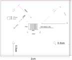
图1为纳米通道的芯片设计示意图;Fig. 1 is the chip design schematic diagram of nano channel;
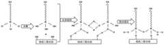
图2为纳米通道表面改性原理图;Figure 2 is a schematic diagram of nanochannel surface modification;
图3为光学显微镜观察的某个时刻的纳米受限通道注水实验图片;Figure 3 is a picture of a nano-restricted channel water injection experiment at a certain moment observed by an optical microscope;
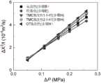
图4为不同条件处理后ΔX2/t与外部压力Pex的关系图。Fig. 4 is a graph showing the relationship between ΔX2 /t and external pressure Pex after treatment under different conditions.
实施方式Implementation
下面将结合附图对本发明的技术方案进行清楚、完整地描述,显然,所描述的实施例是本发明一部分实施例,而不是全部的实施例。基于本发明中的实施例,本领域普通技术人员在没有做出创造性劳动前提下所获得的所有其他实施例,都属于本发明保护的范围。The technical solutions of the present invention will be clearly and completely described below in conjunction with the accompanying drawings. Apparently, the described embodiments are part of the embodiments of the present invention, but not all of them. Based on the embodiments of the present invention, all other embodiments obtained by persons of ordinary skill in the art without making creative efforts belong to the protection scope of the present invention.
本发明的一种纳米通道原位可控疏水改性方法,包括以下步骤:A method for in-situ controllable hydrophobic modification of nanochannels of the present invention comprises the following steps:
A、采用光刻-阳极键合技术加工具有纳米通道的芯片依次置于丙酮、乙醇和蒸馏水中超声清洗十分钟;当芯片放入溶液中后液体会从四个小孔进入微通道和纳米通道,同时超声波会将通道内表面清洗干净,清洗完毕后用氮气吹干;A. Chips with nanochannels processed by photolithography-anodic bonding technology are placed in acetone, ethanol and distilled water for ten minutes of ultrasonic cleaning; when the chip is placed in the solution, the liquid will enter the microchannels and nanochannels from the four small holes , at the same time, the ultrasonic wave will clean the inner surface of the channel, and dry it with nitrogen after cleaning;
上述芯片如图1所示,有16条平行的纳米通道,通过设计掩模板和控制光刻时间,微米通道和纳米通道尺寸可调,每个通道的宽度范围为5-500微米,长度范围为10-4000微米,深度范围为5-1000纳米,通道间隔为10-100微米,纳米通道两端分别于与两条微通道相连(微通道宽为50-500微米,深为1-100微米),微通道两端的二氧化硅被打出四个与外界相连的小孔;The chip above is shown in Figure 1. There are 16 parallel nano-channels. By designing the mask and controlling the lithography time, the size of the micro-channel and nano-channel can be adjusted. The width of each channel ranges from 5 to 500 microns, and the length ranges from 10-4000 microns, the depth range is 5-1000 nanometers, the channel interval is 10-100 microns, the two ends of the nano-channel are respectively connected with two micro-channels (the width of the micro-channel is 50-500 microns, and the depth is 1-100 microns) , the silicon dioxide at both ends of the microchannel is punched with four small holes connected to the outside world;
B、利用微注射泵设备对经过步骤A处理的芯片进行注水实验,同时用高速相机录像功能记录下水进入纳米通道后流动过程,利用MATLAB处理得到不同时间t下弯月面(如图3所示)移动距离ΔX,改变注入压力Pex重复实验;试验结束后将芯片放在去离子水中超声波清洗15分钟,并用氮气吹干;B. Use the micro-injection pump equipment to carry out the water injection experiment on the chip processed in step A. At the same time, use the high-speed camera video function to record the flow process after the water enters the nanochannel, and use MATLAB to process the lower meniscus at different times t (as shown in Figure 3. ) move the distance ΔX, change the injection pressure Pex and repeat the experiment; after the test, put the chip in deionized water and ultrasonically clean it for 15 minutes, and dry it with nitrogen;
C、将Piranha溶液(体积比浓H2SO4:H2O2=7:3)加热到90℃,然后放入步骤B中吹干的芯片并通过水浴加热4小时,同时使用磁力搅拌,转速500r/min,使通道表面被充分羟基化,此时通道表面存在大量-OH;C. Heat the Piranha solution (volume concentration H2 SO4 :H2 O2 =7:3) to 90°C, then put the dried chip in step B and heat it in a water bath for 4 hours while using magnetic stirring, The rotation speed is 500r/min, so that the surface of the channel is fully hydroxylated, and there is a large amount of -OH on the surface of the channel;
其中羟基化方法还包括将芯片浸入硝酸(HNO3)水溶液中使硝酸与通道表面反应形成羟基、氧等离子体处理芯片;The hydroxylation method further includes immersing the chip in an aqueous solution of nitric acid (HNO3 ) so that the nitric acid reacts with the surface of the channel to form hydroxyl groups, and treating the chip with oxygen plasma;
D、将经过步骤C处理的芯片放在500ml去离子水中超声清洗3次,每次10分钟,保证洗掉通道表面残留的Piranha溶液,并用氮气吹干;D. Put the chip treated in step C into 500ml deionized water and ultrasonically clean it 3 times, 10 minutes each time, to ensure that the remaining Piranha solution on the surface of the channel is washed off, and blow dry with nitrogen;
E、利用微注射泵对经过步骤D处理的芯片进行注水实验,同时用高速相机录像功能记录下水进入纳米通道后流动过程,利用MATLAB处理得到不同时间t下弯月面(如图3所示)移动距离ΔX,改变注入压力Pex重复实验;试验结束后将芯片放在去离子水中超声波清洗15分钟,并用氮气吹干;E. Use a micro-syringe pump to perform a water injection experiment on the chip processed in step D. At the same time, use a high-speed camera to record the flow process of water entering the nanochannel, and use MATLAB to obtain the lower meniscus at different times t (as shown in Figure 3) Move the distance ΔX, change the injection pressure Pex and repeat the experiment; after the experiment, put the chip in deionized water for ultrasonic cleaning for 15 minutes, and dry it with nitrogen;
F、将经过步骤E处理的芯片浸入改性剂溶液中完成通道表面的疏水改性,这里的改性剂溶液主要包括三甲基氯硅烷(TMCS)的正己烷溶液或十八烷基三氯硅烷(OTS)的甲苯溶液;F. Immerse the chip treated in step E in the modifier solution to complete the hydrophobic modification of the channel surface. The modifier solution here mainly includes n-hexane solution of trimethylchlorosilane (TMCS) or octadecyl trichloride Toluene solution of silane (OTS);
其中改性原理如图2所示,改性剂多为氯硅烷,容易水解产生-OH,改性剂溶液进入经过步骤B处理的纳米通道后通道表面的-OH和氯硅烷水解产生的-OH发生脱水缩合反应,通道表面被硅烷化,由亲水变为疏水;The modification principle is shown in Figure 2. Most of the modifiers are chlorosilanes, which are easily hydrolyzed to produce -OH. After the modifier solution enters the nanochannels treated in step B, the -OH on the channel surface and the -OH produced by hydrolysis of chlorosilanes A dehydration condensation reaction occurs, and the surface of the channel is silanized, changing from hydrophilic to hydrophobic;
而且设置不同疏水改性时间和改性剂浓度可控制改性后通道表面润湿性,时间范围为15秒至4小时,改性剂浓度范围为0.1wt.%-10wt.%(改性剂浓度范围即三甲基氯硅烷(TMCS)和十八烷基三氯硅烷(OTS)的比例要求);Moreover, setting different hydrophobic modification times and modifier concentrations can control the channel surface wettability after modification, the time range is 15 seconds to 4 hours, and the modifier concentration range is 0.1wt.%-10wt.% (modifier The concentration range is the ratio requirement of trimethylchlorosilane (TMCS) and octadecyltrichlorosilane (OTS);
其他同类型的改性剂还有硅烷类化合物,如六甲基二硅氮烷(HMDS)、(3-氨基丙基)三乙氧基硅烷(APTES)和甲基丙烯酸-3-(三甲氧基甲硅烷基)丙酯(TMSPM),含氟化合物1H,1H,2H,2H-全氟癸基三氯硅烷(FDTS)和1H,1H,2H,2H-全氟辛烷基三氯硅烷(FOTS)。Other modifiers of the same type include silane compounds, such as hexamethyldisilazane (HMDS), (3-aminopropyl) triethoxysilane (APTES) and methacrylic acid-3-(trimethoxy silyl)propyl ester (TMSPM), fluorinated compounds 1H,1H,2H,2H-perfluorodecyltrichlorosilane (FDTS) and 1H,1H,2H,2H-perfluorooctyltrichlorosilane ( FOTS).
G、取出经过步骤F处理的芯片,依次用丙酮、乙醇和去离子水进行超声洗涤15分钟,并用氮气吹干,完成纳米通道疏水改性;G. Take out the chip treated in step F, wash it ultrasonically for 15 minutes with acetone, ethanol and deionized water in sequence, and dry it with nitrogen to complete the hydrophobic modification of the nanochannel;
H、利用微注射泵设备对经过步骤G处理的芯片进行注水实验,同时用高速相机录像功能记录下水进入纳米通道后流动过程,利用MATLAB处理得到不同时间t下弯月面(如图3所示)移动距离ΔX,改变注入压力Pex重复实验;试验结束后将芯片放在去离子水中超声波清洗15分钟,并用氮气吹干。H. Use the micro-injection pump equipment to carry out the water injection experiment on the chip processed by step G, and record the flow process of water entering the nanochannel with the high-speed camera video function at the same time, and use MATLAB to process the lower meniscus at different times t (as shown in Figure 3 ) to move the distance ΔX, and change the injection pressure Pex to repeat the experiment; after the experiment, the chip was ultrasonically cleaned in deionized water for 15 minutes, and dried with nitrogen.
将步骤B、步骤E以及步骤H中不同疏水改性条件下的实验结果整理后得到数据如图4所示;再利用以下公式计算得到未改性、羟基化、以及先羟基化后再进行疏水改性后的表观接触角;After sorting out the experimental results under different hydrophobic modification conditions in Step B, Step E, and Step H, the data are shown in Figure 4; then use the following formula to calculate the unmodified, hydroxylated, and hydroxylated before hydrophobic Modified apparent contact angle;

式中:ΔX为弯月面移动距离,Δt为所用时间,Dh为纳米通道水力直径,Pex为注入压力,μ为表观粘度,λ为水的表面张力,θ为表观接触角。where ΔX is the moving distance of the meniscus, Δt is the elapsed time, Dh is the hydraulic diameter of the nanochannel, Pex is the injection pressure, μ is the apparent viscosity, λ is the surface tension of water, and θ is the apparent contact angle.
其结果如表1所示,不同处理条件下的表观接触角不同,可以通过控制疏水改性时间以及改性剂浓度控制改性后纳米通道表观接触角。The results are shown in Table 1. The apparent contact angles are different under different treatment conditions, and the apparent contact angle of the modified nanochannels can be controlled by controlling the hydrophobic modification time and the concentration of the modifier.
表1、不同条件处理后的表观接触角Table 1. Apparent contact angle after treatment under different conditions

以上所述,并非对本发明作任何形式上的限制,虽然本发明已通过上述实施例揭示,然而并非用以限定本发明,任何熟悉本专业的技术人员,在不脱离本发明技术方案范围内,可利用上述揭示的技术内容作出些变动或修饰为等同变化的等效实施例,但凡是未脱离本发明技术方案的内容,依据本发明的技术实质对以上实施例所作的任何简单修改、等同变化与修饰,均仍属于本发明技术方案的范围内。The above description does not limit the present invention in any form. Although the present invention has been disclosed by the above-mentioned embodiments, it is not intended to limit the present invention. The technical content disclosed above can be used to make some changes or be modified into equivalent embodiments of equivalent changes, but any simple modifications and equivalent changes made to the above embodiments according to the technical essence of the present invention will not deviate from the content of the technical solution of the present invention and modifications, all still belong to the scope of the technical solution of the present invention.
Claims (10)
Translated fromChinesePriority Applications (1)
| Application Number | Priority Date | Filing Date | Title |
|---|---|---|---|
| CN202310129050.9ACN116060148B (en) | 2023-02-17 | 2023-02-17 | A method for in-situ controllable hydrophobic modification of nanochannels |
Applications Claiming Priority (1)
| Application Number | Priority Date | Filing Date | Title |
|---|---|---|---|
| CN202310129050.9ACN116060148B (en) | 2023-02-17 | 2023-02-17 | A method for in-situ controllable hydrophobic modification of nanochannels |
Publications (2)
| Publication Number | Publication Date |
|---|---|
| CN116060148Atrue CN116060148A (en) | 2023-05-05 |
| CN116060148B CN116060148B (en) | 2024-06-07 |
Family
ID=86174785
Family Applications (1)
| Application Number | Title | Priority Date | Filing Date |
|---|---|---|---|
| CN202310129050.9AActiveCN116060148B (en) | 2023-02-17 | 2023-02-17 | A method for in-situ controllable hydrophobic modification of nanochannels |
Country Status (1)
| Country | Link |
|---|---|
| CN (1) | CN116060148B (en) |
Cited By (1)
| Publication number | Priority date | Publication date | Assignee | Title |
|---|---|---|---|---|
| CN117644080A (en)* | 2023-11-27 | 2024-03-05 | 中国地质大学(武汉) | Micro-fluidic chip cleaning device and method based on ultrasonic waves |
Citations (23)
| Publication number | Priority date | Publication date | Assignee | Title |
|---|---|---|---|---|
| WO2001072423A1 (en)* | 2000-03-28 | 2001-10-04 | NMI Naturwissenschaftliches und Medizinisches Institut an der Universität Tübingen | Microfluid components and method for the surface treatment thereof |
| WO2007047644A2 (en)* | 2005-10-14 | 2007-04-26 | The Regents Of The University Of California | Method for microchannel surface modification |
| WO2010017671A1 (en)* | 2008-08-11 | 2010-02-18 | Peking University | Superhydrophobic poly(dimethylsiloxane) and methods for making the same |
| KR20110087963A (en)* | 2010-01-28 | 2011-08-03 | 충남대학교산학협력단 | Selective Surface Modification of Microfluidic Chip Channels and Microfluidic Chips for Double Emulsion Preparation Using the Same |
| US20110244595A1 (en)* | 2010-04-01 | 2011-10-06 | National Cheng Kung University | Biomedical chip for blood coagulation test, method of production and use thereof |
| WO2012013361A2 (en)* | 2010-07-30 | 2012-02-02 | Sony Corporation | A polymeric substrate having a glass-like surface and a chip made of said polymeric substrate |
| KR20120105173A (en)* | 2011-03-15 | 2012-09-25 | 충남대학교산학협력단 | Method for selective surface modification of microfluidic chip channel and preparation of microfluidic chip for multiple emulsion |
| CN102958612A (en)* | 2010-07-23 | 2013-03-06 | 霍夫曼-拉罗奇有限公司 | Method for hydrophilizing surfaces of fluidic components and parts containing such components |
| CN104176944A (en)* | 2014-09-05 | 2014-12-03 | 北京航空航天大学 | Method for modifying OTS self-assembled film on glass substrate |
| CN106861781A (en)* | 2017-04-10 | 2017-06-20 | 黑龙江科技大学 | A kind of microchannel preparation method based on nano surface bubble reduction fluid resistance |
| US20180117797A1 (en)* | 2016-10-13 | 2018-05-03 | Purdue Research Foundation | Methods of making hydrophobic contoured surfaces and hydrophobic contoured surfaces and devices made therefrom |
| CN108246371A (en)* | 2018-01-15 | 2018-07-06 | 西南石油大学 | The microcosmic oil drive chip of setting mark displacing fluid injection rate scale in water conservancy diversion runner |
| CN108472649A (en)* | 2015-10-27 | 2018-08-31 | 伯克利之光生命科技公司 | Microfluidic devices with optimized electrowetting surfaces and related systems and methods |
| CN108579828A (en)* | 2018-04-18 | 2018-09-28 | 清华大学天津高端装备研究院 | A kind of Surface modification of microfluidic chip method that flow velocity is controllable |
| CN108645905A (en)* | 2018-05-24 | 2018-10-12 | 南通大学 | A method of hydrogen peroxide is detected based on solid nano hole |
| CN109025983A (en)* | 2018-07-27 | 2018-12-18 | 中国石油大学(北京) | Method for manufacturing micro model for simulating tight oil reservoir |
| CN109251345A (en)* | 2018-07-24 | 2019-01-22 | 华南理工大学 | A kind of super hydrophilic or super-hydrophobic frosting of durability and preparation method thereof |
| CN111116827A (en)* | 2020-01-06 | 2020-05-08 | 西南石油大学 | High-elasticity high-toughness gel micro-nano particles and preparation method thereof |
| CN111977611A (en)* | 2020-08-31 | 2020-11-24 | 大连理工大学 | A kind of manufacturing method of micro-nano cross-scale polymer spray needle |
| CN113731771A (en)* | 2021-08-20 | 2021-12-03 | 南京理工大学 | Micro-channel with three-dimensional composite wettability surface and preparation method thereof |
| WO2021257326A1 (en)* | 2020-06-17 | 2021-12-23 | Saudi Arabian Oil Company | Nanofluidic chips as micromodels for carbonate reservoirs |
| CN114308154A (en)* | 2021-12-20 | 2022-04-12 | 苏州贝蒂克生物技术有限公司 | Preparation method of double epoxy group modified biochip substrate |
| CN115586110A (en)* | 2022-11-09 | 2023-01-10 | 西南石油大学 | Experimental method for testing gas-liquid diffusion distance and diffusion coefficient based on micro-fluidic |
- 2023
- 2023-02-17CNCN202310129050.9Apatent/CN116060148B/enactiveActive
Patent Citations (23)
| Publication number | Priority date | Publication date | Assignee | Title |
|---|---|---|---|---|
| WO2001072423A1 (en)* | 2000-03-28 | 2001-10-04 | NMI Naturwissenschaftliches und Medizinisches Institut an der Universität Tübingen | Microfluid components and method for the surface treatment thereof |
| WO2007047644A2 (en)* | 2005-10-14 | 2007-04-26 | The Regents Of The University Of California | Method for microchannel surface modification |
| WO2010017671A1 (en)* | 2008-08-11 | 2010-02-18 | Peking University | Superhydrophobic poly(dimethylsiloxane) and methods for making the same |
| KR20110087963A (en)* | 2010-01-28 | 2011-08-03 | 충남대학교산학협력단 | Selective Surface Modification of Microfluidic Chip Channels and Microfluidic Chips for Double Emulsion Preparation Using the Same |
| US20110244595A1 (en)* | 2010-04-01 | 2011-10-06 | National Cheng Kung University | Biomedical chip for blood coagulation test, method of production and use thereof |
| CN102958612A (en)* | 2010-07-23 | 2013-03-06 | 霍夫曼-拉罗奇有限公司 | Method for hydrophilizing surfaces of fluidic components and parts containing such components |
| WO2012013361A2 (en)* | 2010-07-30 | 2012-02-02 | Sony Corporation | A polymeric substrate having a glass-like surface and a chip made of said polymeric substrate |
| KR20120105173A (en)* | 2011-03-15 | 2012-09-25 | 충남대학교산학협력단 | Method for selective surface modification of microfluidic chip channel and preparation of microfluidic chip for multiple emulsion |
| CN104176944A (en)* | 2014-09-05 | 2014-12-03 | 北京航空航天大学 | Method for modifying OTS self-assembled film on glass substrate |
| CN108472649A (en)* | 2015-10-27 | 2018-08-31 | 伯克利之光生命科技公司 | Microfluidic devices with optimized electrowetting surfaces and related systems and methods |
| US20180117797A1 (en)* | 2016-10-13 | 2018-05-03 | Purdue Research Foundation | Methods of making hydrophobic contoured surfaces and hydrophobic contoured surfaces and devices made therefrom |
| CN106861781A (en)* | 2017-04-10 | 2017-06-20 | 黑龙江科技大学 | A kind of microchannel preparation method based on nano surface bubble reduction fluid resistance |
| CN108246371A (en)* | 2018-01-15 | 2018-07-06 | 西南石油大学 | The microcosmic oil drive chip of setting mark displacing fluid injection rate scale in water conservancy diversion runner |
| CN108579828A (en)* | 2018-04-18 | 2018-09-28 | 清华大学天津高端装备研究院 | A kind of Surface modification of microfluidic chip method that flow velocity is controllable |
| CN108645905A (en)* | 2018-05-24 | 2018-10-12 | 南通大学 | A method of hydrogen peroxide is detected based on solid nano hole |
| CN109251345A (en)* | 2018-07-24 | 2019-01-22 | 华南理工大学 | A kind of super hydrophilic or super-hydrophobic frosting of durability and preparation method thereof |
| CN109025983A (en)* | 2018-07-27 | 2018-12-18 | 中国石油大学(北京) | Method for manufacturing micro model for simulating tight oil reservoir |
| CN111116827A (en)* | 2020-01-06 | 2020-05-08 | 西南石油大学 | High-elasticity high-toughness gel micro-nano particles and preparation method thereof |
| WO2021257326A1 (en)* | 2020-06-17 | 2021-12-23 | Saudi Arabian Oil Company | Nanofluidic chips as micromodels for carbonate reservoirs |
| CN111977611A (en)* | 2020-08-31 | 2020-11-24 | 大连理工大学 | A kind of manufacturing method of micro-nano cross-scale polymer spray needle |
| CN113731771A (en)* | 2021-08-20 | 2021-12-03 | 南京理工大学 | Micro-channel with three-dimensional composite wettability surface and preparation method thereof |
| CN114308154A (en)* | 2021-12-20 | 2022-04-12 | 苏州贝蒂克生物技术有限公司 | Preparation method of double epoxy group modified biochip substrate |
| CN115586110A (en)* | 2022-11-09 | 2023-01-10 | 西南石油大学 | Experimental method for testing gas-liquid diffusion distance and diffusion coefficient based on micro-fluidic |
Non-Patent Citations (2)
| Title |
|---|
| WEI BING: "Novel self-assembling polymeric system based on a hydrophobic modified copolymer: formulation, rheological characterization, and performance in enhanced heavy oil recovery", POLYMERS FOR ADVANCED TECHNOLOGIES, vol. 25, no. 1, 31 July 2014 (2014-07-31), pages 732 - 741* |
| 董娟;: "分子印迹材料专利技术分析", 广州化工, no. 16, 23 August 2016 (2016-08-23), pages 32 - 36* |
Cited By (1)
| Publication number | Priority date | Publication date | Assignee | Title |
|---|---|---|---|---|
| CN117644080A (en)* | 2023-11-27 | 2024-03-05 | 中国地质大学(武汉) | Micro-fluidic chip cleaning device and method based on ultrasonic waves |
Also Published As
| Publication number | Publication date |
|---|---|
| CN116060148B (en) | 2024-06-07 |
Similar Documents
| Publication | Publication Date | Title |
|---|---|---|
| CN106944165B (en) | With the liquid function interface of driving directed transport ability and its method and application certainly | |
| CN101037185A (en) | Method for making nano-groove on quartz glass | |
| CN108854854B (en) | A functional fluid gating system | |
| CN108097338B (en) | A micro-nanofluidic chip based on nano-gap between nanostructures and its preparation method | |
| Chen et al. | A rapid and low-cost procedure for fabrication of glass microfluidic devices | |
| CN107442191A (en) | A kind of centrifugal type microfludic chip for Water-In-Oil drop formation | |
| CN116060148B (en) | A method for in-situ controllable hydrophobic modification of nanochannels | |
| CN104998702A (en) | Preparation method of PDMS microfluidic chip based on liquid composite molding method | |
| CN103879953A (en) | Wax-based blade coating patterning method | |
| Lin et al. | Simply realizing durable dual Janus superwettable membranes integrating underwater low-oil-adhesive with super-water-repellent surfaces for controlled oil–water permeation | |
| CN101554543A (en) | Distributed exhaust device for exhausting gas of microfluid device and preparation method thereof | |
| CN111644067A (en) | Preparation method of nano micro-column super-amphiphobic composite membrane | |
| CN109025983B (en) | A method for making a microscopic model for simulating tight oil reservoirs | |
| Abate et al. | Functionalized glass coating for PDMS microfluidic devices | |
| CN106345543B (en) | A kind of microring array chip of the charge inducing electric osmose based on fixed potential | |
| CN101000290A (en) | Sample enrichment chip, manufacturing method and enrichment method and on micronano structure | |
| CN104923324A (en) | Preparation method for PDMS microfluidic chip based on photosensitive resin curing molding | |
| Lu et al. | Shape and surface property effects on displacement enhancement by nanoparticles | |
| CN106861781B (en) | Micro-channel preparation method for reducing fluid resistance based on surface nano-bubbles | |
| CN207680633U (en) | A kind of centrifugal type microfludic chip for Water-In-Oil drop formation | |
| US11389793B2 (en) | Method for producing a microfluidic device | |
| Arayanarakool et al. | A new method of UV-patternable hydrophobization of micro-and nanofluidic networks | |
| CN200982977Y (en) | A micro-current control chip for integrated solid phase extraction pole | |
| CN100999386A (en) | Method of manufacturing glass microractor by etching | |
| Liu et al. | Parylene micropillars coated with thermally grown SiO2 |
Legal Events
| Date | Code | Title | Description |
|---|---|---|---|
| PB01 | Publication | ||
| PB01 | Publication | ||
| SE01 | Entry into force of request for substantive examination | ||
| SE01 | Entry into force of request for substantive examination | ||
| GR01 | Patent grant |