CN116030751A - Display panel - Google Patents
Display panelDownload PDFInfo
- Publication number
- CN116030751A CN116030751ACN202111232655.8ACN202111232655ACN116030751ACN 116030751 ACN116030751 ACN 116030751ACN 202111232655 ACN202111232655 ACN 202111232655ACN 116030751 ACN116030751 ACN 116030751A
- Authority
- CN
- China
- Prior art keywords
- display panel
- signal lines
- shift register
- signal
- lines
- Prior art date
- Legal status (The legal status is an assumption and is not a legal conclusion. Google has not performed a legal analysis and makes no representation as to the accuracy of the status listed.)
- Pending
Links
- 230000002093peripheral effectEffects0.000claimsabstractdescription14
- 239000000463materialSubstances0.000claimsdescription6
- 239000004020conductorSubstances0.000claimsdescription4
- 230000007704transitionEffects0.000claims4
- 238000012546transferMethods0.000description17
- 239000000758substrateSubstances0.000description8
- 239000003990capacitorSubstances0.000description7
- 238000010586diagramMethods0.000description7
- 239000004065semiconductorSubstances0.000description5
- 229910052751metalInorganic materials0.000description4
- 239000002184metalSubstances0.000description4
- 101000805729Homo sapiens V-type proton ATPase 116 kDa subunit a 1Proteins0.000description3
- 101000854879Homo sapiens V-type proton ATPase 116 kDa subunit a 2Proteins0.000description3
- 101000854873Homo sapiens V-type proton ATPase 116 kDa subunit a 4Proteins0.000description3
- 102100020737V-type proton ATPase 116 kDa subunit a 4Human genes0.000description3
- 238000005516engineering processMethods0.000description3
- 101100129007Arabidopsis thaliana LTD geneProteins0.000description2
- 101100505385Mus musculus Gpd1 geneProteins0.000description2
- -1aluminum tin oxideChemical compound0.000description2
- JAONJTDQXUSBGG-UHFFFAOYSA-Ndialuminum;dizinc;oxygen(2-)Chemical compound[O-2].[O-2].[O-2].[O-2].[O-2].[Al+3].[Al+3].[Zn+2].[Zn+2]JAONJTDQXUSBGG-UHFFFAOYSA-N0.000description2
- 239000010408filmSubstances0.000description2
- AMGQUBHHOARCQH-UHFFFAOYSA-Nindium;oxotinChemical compound[In].[Sn]=OAMGQUBHHOARCQH-UHFFFAOYSA-N0.000description2
- 238000004519manufacturing processMethods0.000description2
- 239000007769metal materialSubstances0.000description2
- YVTHLONGBIQYBO-UHFFFAOYSA-Nzinc indium(3+) oxygen(2-)Chemical compound[O--].[Zn++].[In+3]YVTHLONGBIQYBO-UHFFFAOYSA-N0.000description2
- 238000013461designMethods0.000description1
- 238000011161developmentMethods0.000description1
- 230000000694effectsEffects0.000description1
- 239000004973liquid crystal related substanceSubstances0.000description1
- 238000000034methodMethods0.000description1
- 238000012986modificationMethods0.000description1
- 230000004048modificationEffects0.000description1
Images


Landscapes
- Control Of Indicators Other Than Cathode Ray Tubes (AREA)
- Liquid Crystal Display Device Control (AREA)
Abstract
Translated fromChinese
Description
Translated fromChinese技术领域technical field
本发明涉及一种显示技术,尤其涉及一种显示面板。The present invention relates to a display technology, in particular to a display panel.
背景技术Background technique
许多工艺技术的突破带动了显示技术的蓬勃发展。其中,为了满足窄边框显示的需求以及降低生产成本,将驱动显示面板所用的栅极驱动电路(gate driver circuit)制作在显示面板的周边线路区内的技术被提出。然而,栅极驱动电路的控制信号(例如:时脉信号)因其脉波的变化较为频繁而容易对邻近的显示驱动电路产生电磁干扰(electromagnetic interference,EMI),造成显示质量的下降。Many technological breakthroughs have led to the vigorous development of display technology. Among them, in order to meet the demand for narrow frame display and reduce production cost, a technology of manufacturing a gate driver circuit (gate driver circuit) used for driving the display panel in the peripheral circuit area of the display panel has been proposed. However, the control signal (for example, clock signal) of the gate driving circuit tends to generate electromagnetic interference (EMI) to the adjacent display driving circuit due to its frequent pulse changes, resulting in a decrease in display quality.
发明内容Contents of the invention
本发明是针对一种显示面板,其具有较稳定的操作电性。The invention is directed to a display panel with relatively stable operating electrical properties.
根据本发明的实施例,显示面板具有显示区以及显示区以外的周边区,且包括多条信号线、多个移位暂存电路以及辅助电极。这些信号线设置于周边区,并且电性连接这些移位暂存电路。这些移位暂存电路接收来自这些信号线的多个控制信号,并输出多个栅极驱动信号至显示区。辅助电极覆盖这些信号线。辅助电极电性绝缘于这些信号线,并且具有浮置电位或固定电位。According to an embodiment of the present invention, the display panel has a display area and a peripheral area other than the display area, and includes a plurality of signal lines, a plurality of shift register circuits and auxiliary electrodes. The signal lines are arranged in the peripheral area and electrically connected with the shift register circuits. The shift register circuits receive a plurality of control signals from the signal lines, and output a plurality of gate driving signals to the display area. Auxiliary electrodes cover these signal lines. The auxiliary electrodes are electrically insulated from these signal lines, and have a floating potential or a fixed potential.
在根据本发明的实施例的显示面板中,多条信号线包括多条时脉信号线。多个移位暂存电路分别接收来自这些时脉信号线的多个时脉信号。In a display panel according to an embodiment of the present invention, the plurality of signal lines includes a plurality of clock signal lines. The multiple shift register circuits respectively receive multiple clock signals from the clock signal lines.
在根据本发明的实施例的显示面板中,每一个移位暂存电路包括上拉电路以及输出级电路。上拉电路依据扫描方向信号上拉第一驱动信号。输出级电路依据多个时脉信号的其中一者和第一驱动信号产生多个栅极驱动信号的其中一者。In the display panel according to the embodiment of the present invention, each shift register circuit includes a pull-up circuit and an output stage circuit. The pull-up circuit pulls up the first driving signal according to the scan direction signal. The output stage circuit generates one of the plurality of gate driving signals according to one of the plurality of clock signals and the first driving signal.
在根据本发明的实施例的显示面板中,多条时脉信号线经由多条连接线与多个移位暂存电路的多个输出级电路电性连接。辅助电极还覆盖多条连接线,且电性绝缘于这些连接线。In the display panel according to the embodiment of the present invention, the multiple clock signal lines are electrically connected to the multiple output stage circuits of the multiple shift register circuits via multiple connecting wires. The auxiliary electrode also covers a plurality of connecting wires and is electrically insulated from these connecting wires.
在根据本发明的实施例的显示面板中,多条连接线经由多个转接图案与多条时脉信号线电性连接。辅助电极还覆盖这些转接图案,且电性绝缘于这些转接图案。In the display panel according to the embodiment of the present invention, the plurality of connection lines are electrically connected to the plurality of clock signal lines via a plurality of transfer patterns. The auxiliary electrodes also cover the transfer patterns and are electrically insulated from the transfer patterns.
在根据本发明的实施例的显示面板中,多条连接线经由多个转接图案与多条时脉信号线电性连接,且辅助电极与这些转接图案为同一膜层。In the display panel according to the embodiment of the present invention, the multiple connection lines are electrically connected to the multiple clock signal lines through the multiple transfer patterns, and the auxiliary electrode and the transfer patterns are in the same film layer.
在根据本发明的实施例的显示面板中,每一个移位暂存电路还包括至少一下拉电路。下拉电路电性连接多条信号线的第一电源线和第二电源线,并且依据来自第一电源线的第一控制信号和来自第二电源线的第二控制信号下拉第一驱动信号。In the display panel according to an embodiment of the present invention, each shift register circuit further includes at least one pull-down circuit. The pull-down circuit is electrically connected to the first power line and the second power line of the plurality of signal lines, and pulls down the first driving signal according to the first control signal from the first power line and the second control signal from the second power line.
在根据本发明的实施例的显示面板中,第一控制信号和第二控制信号的电压电平的切换频率低于显示面板的画面更新频率。In the display panel according to an embodiment of the present invention, the switching frequency of the voltage levels of the first control signal and the second control signal is lower than the frame update frequency of the display panel.
在根据本发明的实施例的显示面板中,辅助电极还覆盖多个移位暂存电路,且电性绝缘于这些移位暂存电路。In the display panel according to the embodiment of the present invention, the auxiliary electrode also covers a plurality of shift register circuits and is electrically insulated from these shift register circuits.
在根据本发明的实施例的显示面板中,辅助电极的材质包括透光导电材料。In the display panel according to an embodiment of the present invention, the material of the auxiliary electrode includes a light-transmitting conductive material.
基于上述,本发明的一实施例的显示面板在周边区设有多个移位暂存电路。这些移位暂存电路适于接收来自多条信号线的多个控制信号并输出用于显示画面所需的栅极驱动信号。通过将具有浮置电位或固定电位的辅助电极覆盖在这些信号线上,可有效抑制这些信号线因传送脉波变化较为频繁的控制信号而产生的电磁干扰(EMI),从而提升显示面板的驱动稳定性。Based on the above, the display panel according to an embodiment of the present invention is provided with a plurality of shift register circuits in the peripheral area. These shift register circuits are adapted to receive a plurality of control signals from a plurality of signal lines and output gate driving signals required for displaying images. By covering these signal lines with auxiliary electrodes with floating potential or fixed potential, the electromagnetic interference (EMI) generated by these signal lines due to the control signals with frequent pulse changes can be effectively suppressed, thereby improving the drive of the display panel. stability.
附图说明Description of drawings
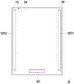
图1是依照本发明的第一实施例的显示面板的俯视示意图;1 is a schematic top view of a display panel according to a first embodiment of the present invention;
图2是图1的显示面板的局部放大示意图;FIG. 2 is a partially enlarged schematic diagram of the display panel of FIG. 1;
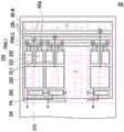
图3是图2的周边区的局部放大示意图;Fig. 3 is a partially enlarged schematic diagram of the peripheral area in Fig. 2;
图4是图3的显示面板的剖视示意图;4 is a schematic cross-sectional view of the display panel in FIG. 3;
图5是图2的移位暂存电路的电路简图;Fig. 5 is the schematic circuit diagram of the shift register circuit of Fig. 2;
图6是图1的栅极驱动电路的驱动波形示意图;FIG. 6 is a schematic diagram of driving waveforms of the gate driving circuit of FIG. 1;
图7是依照本发明的第二实施例的显示面板的俯视示意图;7 is a schematic top view of a display panel according to a second embodiment of the present invention;
图8是图7的显示面板的局部放大示意图;FIG. 8 is a partially enlarged schematic diagram of the display panel of FIG. 7;
图9是图8的显示面板的剖视示意图;9 is a schematic cross-sectional view of the display panel in FIG. 8;
图10是依照本发明的第三实施例的显示面板的俯视示意图。FIG. 10 is a schematic top view of a display panel according to a third embodiment of the present invention.
附图标记说明Explanation of reference signs
10、20、30:显示面板;10, 20, 30: display panel;
100、100A:像素阵列基板;100, 100A: pixel array substrate;
110、120、130:绝缘层;110, 120, 130: insulating layer;
110a、120a、120b:接触孔;110a, 120a, 120b: contact holes;
200:移位暂存电路;200: shift temporary storage circuit;
210:上拉电路;210: pull-up circuit;
220:输出级电路;220: output stage circuit;
230、231、232:下拉电路;230, 231, 232: pull-down circuits;
AE、AE-A、AE-B:辅助电极;AE, AE-A, AE-B: auxiliary electrodes;
AEa:开口;AEa: opening;
BLK:遮没时间;BLK: Blanking time;
C:电容器;C: capacitor;
CK、CK1~CK4:时脉信号;CK, CK1~CK4: clock signal;
CKL:时脉信号线;CKL: clock signal line;
CL1、CL2:连接线;CL1, CL2: connection line;
D2U、U2D:扫描方向信号D2U, U2D: scan direction signal
DA:显示区;DA: display area;
DS1:第一驱动信号;DS1: the first driving signal;
DS2:第二驱动信号;DS2: the second driving signal;
Ea:第一端电极;Ea: first terminal electrode;
Eb:第二端电极;Eb: second terminal electrode;
Ec:控制端电极;Ec: control terminal electrode;
FP:画面周期;FP: picture period;
Gn、Gn+1、Gn-1:栅极驱动信号;Gn, Gn+1, Gn-1: gate drive signal;
GDC1、GDC2:栅极驱动电路;GDC1, GDC2: gate drive circuit;
PA:周边区;PA: peripheral area;
PWL1、PWL2、PWL3:电源线;PWL1, PWL2, PWL3: power cords;
SB:基板;SB: Substrate;
SC:半导体图案;SC: semiconductor pattern;
SIC:源极驱动芯片;SIC: source driver chip;
T、T1~T13:晶体管;T, T1~T13: Transistors;
TP:转接图案;TP: transfer pattern;
VPWL1、VPWL2:控制信号;VPWL1, VPWL2: control signal;
VSS:系统低电压;VSS: system low voltage;
A-A’、B-B’:剖线。A-A', B-B': section line.
具体实施方式Detailed ways
在本申请说明书全文中所使用的“耦接(或连接)”一词可指任何直接或间接的连接手段。举例而言,若文中描述第一装置耦接(或连接)于第二装置,则应该被解释成所述第一装置可以直接连接于所述第二装置,或者所述第一装置可以通过其他装置或某种连接手段而间接地连接至所述第二装置。本申请说明书全文中提及的“第一”、“第二”等用语是用以命名组件(element)的名称,或区别不同实施例或范围,而并非用来限制组件数量的上限或下限,也非用来限制组件的次序。As used throughout the specification of this application, the term "coupled (or connected)" may refer to any means of connection, direct or indirect. For example, if it is described herein that a first device is coupled (or connected) to a second device, it should be interpreted that the first device can be directly connected to the second device, or that the first device can be connected via other devices. device or some connection means is indirectly connected to the second device. Terms such as "first" and "second" mentioned throughout the specification of this application are used to name components (elements), or to distinguish different embodiments or ranges, and are not used to limit the upper or lower limit of the number of components. Nor is it intended to limit the order of components.
现将详细地参考本发明的示范性实施例,示范性实施例的实例说明于附图中。只要有可能,相同元件符号在附图和描述中用来表示相同或相似部分。Reference will now be made in detail to the exemplary embodiments of the present invention, examples of which are illustrated in the accompanying drawings. Wherever possible, the same reference numbers will be used in the drawings and description to refer to the same or like parts.
图1是依照本发明的第一实施例的显示面板的俯视示意图。图2是图1的显示面板的局部放大示意图。图3是图2的周边区的局部放大示意图。图4是图3的显示面板的剖视示意图。图5是图2的移位暂存电路的电路简图。图6是图1的栅极驱动电路的驱动波形示意图。图4对应图3的剖线A-A’。FIG. 1 is a schematic top view of a display panel according to a first embodiment of the invention. FIG. 2 is a partially enlarged schematic view of the display panel in FIG. 1 . FIG. 3 is a partially enlarged schematic view of the peripheral area in FIG. 2 . FIG. 4 is a schematic cross-sectional view of the display panel in FIG. 3 . FIG. 5 is a schematic circuit diagram of the shift register circuit in FIG. 2 . FIG. 6 is a schematic diagram of driving waveforms of the gate driving circuit in FIG. 1 . Fig. 4 corresponds to section line A-A' of Fig. 3 .
请参照图1,显示面板10包括像素阵列基板100和显示介质层(未示出)。显示面板10具有显示区DA以及显示区DA以外的周边区PA。举例来说,像素阵列基板100在周边区PA内设有栅极驱动电路GDC1、栅极驱动电路GDC2及源极驱动芯片SIC。像素阵列基板100在显示区DA内可设有多个像素结构(未示出)以及显示介质层。这两个栅极驱动电路分别设置在显示区DA在一方向上的相对两侧,而源极驱动芯片SIC设置在显示区DA在另一方向上的一侧,但不以此为限。在其他实施例中,显示面板也可仅具有一个栅极驱动电路。Referring to FIG. 1 , the
位于显示区DA的这些像素结构分别电性耦接这两个栅极驱动电路和源极驱动电路SIC。举例来说,显示面板10可通过这些栅极驱动电路和源极驱动电路SIC个别地控制这些像素结构来驱使显示介质层发光或调变光线,以达到显示图像的效果。也即,显示介质层可以是多个发光二极管(例如微型发光二极管、有机发光二极管或次毫米发光二极管)或液晶层,本发明并不加以限制。The pixel structures located in the display area DA are respectively electrically coupled to the two gate driving circuits and the source driving circuit SIC. For example, the
请参照图2、图5及图6,这些栅极驱动电路各自包括多条信号线和多个移位暂存电路200。这些移位暂存电路分别电性连接这些信号线,且彼此串联耦接。这些移位暂存电路200适于接收来自这些信号线的多个控制信号,并输出多个栅极驱动信号(如图5示出的栅极驱动信号Gn、栅极驱动信号Gn+1和栅极驱动信号Gn-1)至显示区DA内的多个像素结构。在本实施例中,这些信号线包括多条时脉信号线CKL,且用于传送时脉信号CK(如图6示出的时脉信号CK1、时脉信号CK2、时脉信号CK3和时脉信号CK4)至对应的移位暂存电路200。Please refer to FIG. 2 , FIG. 5 and FIG. 6 , each of these gate driving circuits includes a plurality of signal lines and a plurality of
在本实施例中,移位暂存电路200可包括多个晶体管T和电容器C。这些晶体管T(例如晶体管T1~晶体管T13)和电容器C分别构成移位暂存电路200的上拉电路210、输出级电路220和下拉电路230。上拉电路210适于依据扫描方向信号(例如:第一扫描方向信号U2D或第二扫描方向信号D2U)上拉第一驱动信号DS1。输出级电路220适于依据对应的时脉信号CK、第一驱动信号DS1和第二驱动信号DS2产生栅极驱动信号Gn。In this embodiment, the
晶体管T可包括第一端电极Ea、第二端电极Eb、控制端电极Ec和半导体图案SC。第一端电极Ea和第二端电极Eb设置在半导体图案SC的一侧,且电性连接半导体图案SC的不同两区(例如源极区和漏极区)。控制端电极Ec设置在半导体图案SC的另一侧,并且与第一端电极Ea和第二端电极Eb相对。举例来说,在本实施例中,晶体管T为底部栅极型薄膜晶体管(bottom-gate thin film transistor),但不以此为限。在其他实施例中,晶体管T也可以是顶部栅极型薄膜晶体管(top-gate thin film transistor)。The transistor T may include a first terminal electrode Ea, a second terminal electrode Eb, a control terminal electrode Ec, and a semiconductor pattern SC. The first terminal electrode Ea and the second terminal electrode Eb are disposed on one side of the semiconductor pattern SC, and are electrically connected to two different regions of the semiconductor pattern SC (such as a source region and a drain region). The control terminal electrode Ec is disposed on the other side of the semiconductor pattern SC, and is opposite to the first terminal electrode Ea and the second terminal electrode Eb. For example, in this embodiment, the transistor T is a bottom-gate thin film transistor (bottom-gate thin film transistor), but not limited thereto. In other embodiments, the transistor T may also be a top-gate thin film transistor.
在本实施例中,移位暂存电路200的下拉电路230数量是以两个(分别为下拉电路231和下拉电路232)为例进行示例性地说明,并不表示本发明以此为限制。在其他实施例中,移位暂存电路的下拉电路数量也可以是一个。另一方面,本发明也不加以限制每一个移位暂存电路200所具有的晶体管T和电容器C的数量,这些元件的数量当可根据产品的实际电路设计来调整。In this embodiment, the number of pull-down
请同时参照图3,栅极驱动电路的多条信号线还包括第一电源线PWL1、第二电源线PWL2和第三电源线PWL3。下拉电路230电性连接这些电源线,并且依据来自第一电源线PWL1的第一控制信号VPWL1和来自第二电源线PWL2的第二控制信号VPWL2下拉第一驱动信号DS1并输出第二驱动信号DS2。输出级电路220依据来自上拉电路210的第一驱动信号DS1和来自下拉电路230的第二驱动信号DS2来产生第N级栅极驱动信号Gn,其中N为大于1的正整数。Please refer to FIG. 3 at the same time, the multiple signal lines of the gate driving circuit further include a first power line PWL1 , a second power line PWL2 and a third power line PWL3 . The pull-
详细而言,上拉电路210包括晶体管T2和晶体管T3。晶体管T2的控制端接收来自前一级移位暂存电路200输出的栅极驱动信号Gn-1,晶体管T2的第一端接收第一扫描方向信号U2D,晶体管T2的第二端连接晶体管T1的第二端、输出级电路220和下拉电路230。晶体管T3的控制端接收来自后一级移位暂存电路200输出的栅极驱动信号Gn+1,晶体管T3的第一端接收第二扫描方向信号D2U。此处的栅极驱动信号Gn-1和栅极驱动信号Gn+1分别为第N-1级和第N+1级的移位暂存电路200所产生的栅极驱动信号。在本实施例中,第一扫描方向信号U2D用以指示栅极驱动电路的扫描方向为第一方向(例如从图1的上方朝下方进行扫描),而第二扫描方向信号D2U用以指示栅极驱动电路的扫描方向为第二方向(例如从图1的下方朝上方进行扫描)。In detail, the pull-up
输出级电路220包括晶体管T1、晶体管T4、晶体管T5和电容器C。晶体管T1的控制端连接电容器C的第一端、下拉电路230,晶体管T1的第一端接收来自时脉信号线CKL的时脉信号CK,晶体管T1的第二端连接电容器C的第二端、晶体管T4的第一端、晶体管T5的第一端,并且输出栅极驱动信号Gn。晶体管T4的控制端接收来自下拉电路231的第二驱动信号DS2,晶体管T4的第二端耦接至系统低电压VSS。相似地,晶体管T5的控制端接收来自下拉电路231的第二驱动信号DS2,晶体管T5的第二端耦接至系统低电压VSS。The
下拉电路231包括晶体管T6、晶体管T8、晶体管T10和晶体管T12。晶体管T6的控制端连接晶体管T8的第一端、上拉电路210和输出级电路220,并接收来自上拉电路210的第一驱动信号DS1。晶体管T6的第一端连接晶体管T4的控制端、晶体管T8的控制端、晶体管T12的第一端和晶体管T10的第一端,晶体管T6的第二端耦接至系统低电压VSS。晶体管T8的第二端耦接至系统低电压VSS。晶体管T10的控制端接收第二控制信号VPWL2和晶体管T10的第二端。晶体管T12的控制端接收第一控制信号VPWL1,晶体管T12的第二端耦接至系统低电压VSS。The pull-
相似地,下拉电路232包括晶体管T7、晶体管T9、晶体管T11和晶体管T13。晶体管T7的控制端连接晶体管T9的第一端、上拉电路210和输出级电路220,并接收来自上拉电路210的第一驱动信号DS1。晶体管T7的第一端连接晶体管T5的控制端、晶体管T9的控制端、晶体管T13的第一端和晶体管T11的第一端,晶体管T7的第二端耦接至系统低电压VSS。晶体管T9的第二端耦接至系统低电压VSS。晶体管T11的控制端接收第一控制信号VPWL1和晶体管T11的第二端。晶体管T13的控制端接收第二控制信号VPWL2,晶体管T13的第二端耦接至系统低电压VSS。Similarly, the pull-
举例来说,当栅极驱动电路接收到扫描起始信号STV1,多条时脉信号线CKL依序开始传送时脉信号CK1~CK4。相互串联耦接的多个移位暂存电路200在时序上依序输出栅极驱动信号至显示区DA以个别地控制多个像素结构并经由显示介质层来显示图像。在最后一级的移位暂存电路200输出栅极驱动信号后,栅极驱动电路会接收到扫描终止信号STV2,此时便完成一个画面周期(frame period)FP的图像更新。也就是说,扫描起始信号STV1和扫描终止信号STV2于时序上的间隔范围可定义为一个画面周期FP。For example, when the gate driving circuit receives the scan start signal STV1 , the plurality of clock signal lines CKL sequentially start to transmit the clock signals CK1 - CK4 . The plurality of
特别注意的是,在一个画面周期FP内,时脉信号CK1~CK4的电压电平的切换频率明显高出画面更新频率许多。为了抑制这些脉波变化较为频繁的时脉信号CK所产生的电磁干扰(electromagnetic interference,EMI),这些时脉信号线CKL上设有辅助电极AE。如图3及图4所示,在本实施例中,辅助电极AE可覆盖多条时脉信号线CKL,以屏蔽这些时脉信号线CKL对其他电子元件的电磁干扰,从而提升显示面板10的驱动稳定性。然而,本发明不限于此。在其他实施例中,辅助电极还可整面性地覆盖在设有栅极驱动电路的区域内。It should be noted that, within one frame period FP, the switching frequency of the voltage levels of the clock signals CK1 - CK4 is significantly higher than the frame update frequency. In order to suppress electromagnetic interference (EMI) generated by these clock signals CK with relatively frequent pulse changes, auxiliary electrodes AE are provided on these clock signal lines CKL. As shown in FIG. 3 and FIG. 4 , in this embodiment, the auxiliary electrode AE can cover a plurality of clock signal lines CKL to shield the electromagnetic interference of these clock signal lines CKL to other electronic components, thereby improving the performance of the
举例来说,电性绝缘于这些时脉信号线CKL的辅助电极AE可具有浮置电位(floating potential),但不以此为限。在其他实施例中,辅助电极AE也可接地或耦接至一电压源而具有固定电位。For example, the auxiliary electrodes AE electrically insulated from the clock signal lines CKL may have floating potentials, but not limited thereto. In other embodiments, the auxiliary electrode AE can also be grounded or coupled to a voltage source to have a fixed potential.
在本实施例中,这些时脉信号线CKL可经由多条连接线CL1与多个移位暂存电路200的多个输出级电路220电性连接。更具体地说,这些连接线CL1是经由多个转接图案TP与这些时脉信号线CKL电性连接,且辅助电极AE还覆盖这些转接图案TP。举例来说,像素阵列基板100可包括依序设置于基板SB上的第一金属导电层、第一绝缘层110、第二金属导电层、第二绝缘层120、第三导电层和第三绝缘层130。多条时脉信号线CKL、电源线PWL1和电源线PWL2属于第一金属导电层。多条连接线CL1和电源线PWL3属于第二金属导电层。多个转接图案TP属于第三导电层。辅助电极AE是设置在第三绝缘层130上。In this embodiment, the clock signal lines CKL are electrically connected to the
也就是说,转接图案TP是设置在辅助电极AE与连接线CL1(或时脉信号线CKL)之间。为了实现时脉信号线CKL与连接线CL1的电性连接关系,转接图案TP的一部分可经由第二绝缘层120的接触孔120a与连接线CL1电性连接,而转接图案TP的另一部分可经由第二绝缘层120的接触孔120b和第一绝缘层110的接触孔110a与时脉信号线CKL电性连接,但不以此为限。在本实施例中,辅助电极AE的材质包括透光导电材料,透光导电材料例如是铟锡氧化物、铟锌氧化物、铝锡氧化物、铝锌氧化物、或其它合适的氧化物、或者是上述至少两者的堆叠层。然而,本发明不限于此。在其他实施例中,辅助电极AE的材质也可包括金属材料。That is to say, the transfer pattern TP is disposed between the auxiliary electrode AE and the connection line CL1 (or the clock signal line CKL). In order to realize the electrical connection relationship between the clock signal line CKL and the connection line CL1, a part of the transfer pattern TP can be electrically connected to the connection line CL1 through the
在本实施例中,第三导电层的材质包括透光导电材料,透光导电材料例如是铟锡氧化物、铟锌氧化物、铝锡氧化物、铝锌氧化物、或其它合适的氧化物、或者是上述至少两者的堆叠层。然而,本发明不限于此。在其他实施例中,第三导电层的材质也可包括金属材料。In this embodiment, the material of the third conductive layer includes a transparent conductive material, such as indium tin oxide, indium zinc oxide, aluminum tin oxide, aluminum zinc oxide, or other suitable oxides. , or a stacked layer of at least two of the above. However, the present invention is not limited thereto. In other embodiments, the material of the third conductive layer may also include metal materials.
另一方面,第一电源线PWL1和第二电源线PWL2也可经由多条连接线CL2与多个移位暂存电路200的下拉电路231的晶体管T10(或图5的晶体管T12)和下拉电路232的晶体管T11(或图5的晶体管T13)电性连接,且这些电源线也是经由多个转接图案TP与这些连接线CL2电性连接。由于转接图案TP、连接线CL2和电源线的连接关系相似于转接图案TP、连接线CL1和时脉信号线CKL的连接关系,因此,详细的说明请参见前述的相关段落,于此便不再赘述。On the other hand, the first power line PWL1 and the second power line PWL2 can also connect the transistor T10 (or the transistor T12 of FIG. The transistor T11 of 232 (or the transistor T13 in FIG. 5 ) is electrically connected, and the power lines are also electrically connected to the connection lines CL2 via a plurality of transfer patterns TP. Since the connection relationship between the transfer pattern TP, the connection line CL2 and the power line is similar to the connection relationship between the transfer pattern TP, the connection line CL1 and the clock signal line CKL, please refer to the relevant paragraphs above for detailed descriptions, hereby No longer.
以下将列举另一些实施例以详细说明本揭露,其中相同的构件将标示相同的符号,并且省略相同技术内容的说明,省略部分请参考前述实施例,以下不再赘述。Some other embodiments will be listed below to describe the present disclosure in detail, wherein the same components will be marked with the same symbols, and the description of the same technical content will be omitted.
图7是依照本发明的第二实施例的显示面板的俯视示意图。图8是图7的显示面板的局部放大示意图。图9是图8的显示面板的剖视示意图。图9对应图8的剖线B-B’。请参照图7至图9,本实施例的显示面板20与图2及图3的显示面板10的差异在于:辅助电极的设置方式不同。在本实施例中,显式面板20的转接图案TP与辅助电极AE-A可选地为同一膜层。FIG. 7 is a schematic top view of a display panel according to a second embodiment of the present invention. FIG. 8 is a partially enlarged schematic view of the display panel in FIG. 7 . FIG. 9 is a schematic cross-sectional view of the display panel in FIG. 8 . Fig. 9 corresponds to the section line B-B' of Fig. 8 . Please refer to FIG. 7 to FIG. 9 , the difference between the display panel 20 of this embodiment and the
举例来说,显示面板20的像素阵列基板100A并未设有图4的第三绝缘层130和第三导电层,且辅助电极AE-A是设置在第二绝缘层120上。也因此,不同于前述实施例,辅助电极AE-A具有多个开口AEa,且多个转接图案TP位于这些开口AEa内,且电性绝缘于辅助电极AE-A。For example, the
为了进一步抑制具有较高切换频率的时脉信号CK所产生的电磁干扰,本实施例的辅助电极AE-A还尽可能地覆盖设有多条连接线CL1的区域。也就是说,辅助电极AE-A会沿着连接线CL1的延伸路径进行遮盖。In order to further suppress the electromagnetic interference generated by the clock signal CK with a relatively high switching frequency, the auxiliary electrode AE-A of this embodiment also covers the area where a plurality of connecting lines CL1 are provided as much as possible. That is to say, the auxiliary electrode AE-A will be covered along the extension path of the connection line CL1.
请同时参照图6,特别说明的是,第一电源线PWL1和第二电源线PWL2所传输的第一控制信号VPWL1和第二控制信号VPWL2各自在一个画面周期FP和一个遮没时间(blankingtime)BLK后会进行一次电压电平的切换。也就是说,第一控制信号VPWL1和第二控制信号VPWL2的电压电平的切换频率低于显示面板10的画面更新频率。在本实施例中,每一个画面周期FP的扫描终止信号STV2与下一个画面周期FP的扫描起始信号STV1于时序上的间隔范围可定义为一个遮没时间BLK,但不以此为限。Please refer to FIG. 6 at the same time. It is particularly illustrated that the first control signal VPWL1 and the second control signal VPWL2 transmitted by the first power line PWL1 and the second power line PWL2 are respectively within a frame period FP and a blanking time. After BLK, a voltage level switching will be performed. That is to say, the switching frequency of the voltage levels of the first control signal VPWL1 and the second control signal VPWL2 is lower than the frame update frequency of the
因此,本实施例的辅助电极AE-A还可覆盖第一电源线PWL1和第二电源线PWL2来屏蔽具有较低切换频率的第一控制信号VPWL1和第二控制信号VPWL2所产生的电磁干扰,有助于进一步提升显示面板20的驱动稳定性。Therefore, the auxiliary electrode AE-A of this embodiment can also cover the first power line PWL1 and the second power line PWL2 to shield the electromagnetic interference generated by the first control signal VPWL1 and the second control signal VPWL2 with lower switching frequency, It helps to further improve the driving stability of the display panel 20 .
图10是依照本发明的第三实施例的显示面板的俯视示意图。请参照图10,本实施例的显示面板30与图7的显示面板20的差异在于:显示面板30的辅助电极AE-B还覆盖多个移位暂存电路200,且电性绝缘于这些移位暂存电路200。更具体地说,辅助电极AE-B大致上整面性地覆盖在设有栅极驱动电路的区域内。由于这些移位暂存电路200各自在一个画面周期FP内会进行至少一次的电压电平的切换,例如:上拉和下拉第一驱动信号DS1来产生栅极驱动信号,因此,通过辅助电极AE-B的设置可进一步抑制移位暂存电路200在一个画面周期FP内的信号调整所产生的电磁干扰,有助于提升显示面板30的驱动稳定性。FIG. 10 is a schematic top view of a display panel according to a third embodiment of the present invention. Please refer to FIG. 10, the difference between the
纵上所述,本发明的一实施例的显示面板在周边区设有多个移位暂存电路。这些移位暂存电路适于接收来自多条信号线的多个控制信号并输出用于显示画面所需的栅极驱动信号。通过将具有浮置电位或固定电位的辅助电极覆盖在这些信号线上,可有效抑制这些信号线因传送脉波变化较为频繁的控制信号而产生的电磁干扰(EMI),从而提升显示面板的驱动稳定性。As mentioned above, the display panel according to an embodiment of the present invention is provided with a plurality of shift register circuits in the peripheral area. These shift register circuits are adapted to receive a plurality of control signals from a plurality of signal lines and output gate driving signals required for displaying images. By covering these signal lines with auxiliary electrodes with floating potential or fixed potential, the electromagnetic interference (EMI) generated by these signal lines due to the control signals with frequent pulse changes can be effectively suppressed, thereby improving the drive of the display panel. stability.
最后应说明的是:以上各实施例仅用以说明本发明的技术方案,而非对其限制;尽管参照前述各实施例对本发明进行了详细的说明,本领域的普通技术人员应当理解:其依然可以对前述各实施例所记载的技术方案进行修改,或者对其中部分或者全部技术特征进行等同替换;而这些修改或者替换,并不使相应技术方案的本质脱离本发明各实施例技术方案的范围。Finally, it should be noted that: the above embodiments are only used to illustrate the technical solutions of the present invention, rather than limiting them; although the present invention has been described in detail with reference to the foregoing embodiments, those of ordinary skill in the art should understand that: It is still possible to modify the technical solutions described in the foregoing embodiments, or perform equivalent replacements for some or all of the technical features; and these modifications or replacements do not make the essence of the corresponding technical solutions deviate from the technical solutions of the various embodiments of the present invention. scope.
Claims (10)
Translated fromChinesePriority Applications (1)
| Application Number | Priority Date | Filing Date | Title |
|---|---|---|---|
| CN202111232655.8ACN116030751A (en) | 2021-10-22 | 2021-10-22 | Display panel |
Applications Claiming Priority (1)
| Application Number | Priority Date | Filing Date | Title |
|---|---|---|---|
| CN202111232655.8ACN116030751A (en) | 2021-10-22 | 2021-10-22 | Display panel |
Publications (1)
| Publication Number | Publication Date |
|---|---|
| CN116030751Atrue CN116030751A (en) | 2023-04-28 |
Family
ID=86076330
Family Applications (1)
| Application Number | Title | Priority Date | Filing Date |
|---|---|---|---|
| CN202111232655.8APendingCN116030751A (en) | 2021-10-22 | 2021-10-22 | Display panel |
Country Status (1)
| Country | Link |
|---|---|
| CN (1) | CN116030751A (en) |
Citations (3)
| Publication number | Priority date | Publication date | Assignee | Title |
|---|---|---|---|---|
| WO2008073157A2 (en)* | 2006-08-14 | 2008-06-19 | Georgia Tech Research Corporation | Electrochemical biosensor arrays and systems and methods of making same |
| CN105070761A (en)* | 2009-07-31 | 2015-11-18 | 株式会社半导体能源研究所 | Display device |
| CN108181767A (en)* | 2016-12-08 | 2018-06-19 | 三星显示有限公司 | Display device |
- 2021
- 2021-10-22CNCN202111232655.8Apatent/CN116030751A/enactivePending
Patent Citations (3)
| Publication number | Priority date | Publication date | Assignee | Title |
|---|---|---|---|---|
| WO2008073157A2 (en)* | 2006-08-14 | 2008-06-19 | Georgia Tech Research Corporation | Electrochemical biosensor arrays and systems and methods of making same |
| CN105070761A (en)* | 2009-07-31 | 2015-11-18 | 株式会社半导体能源研究所 | Display device |
| CN108181767A (en)* | 2016-12-08 | 2018-06-19 | 三星显示有限公司 | Display device |
Similar Documents
| Publication | Publication Date | Title |
|---|---|---|
| US12225811B2 (en) | Display apparatus and electronic apparatus | |
| CN210956110U (en) | a display device | |
| US10840265B2 (en) | Display panel and method of improving display quality in peripheral regions thereof | |
| CN102339848B (en) | Organic elctroluminescent device and manufacture method thereof and electronic equipment | |
| CN114822395B (en) | Display panel | |
| CN115425063B (en) | Display panel and display device | |
| US20250239217A1 (en) | Display panel and display device | |
| WO2021042523A1 (en) | Display panel | |
| US20250268024A1 (en) | Display panel, pixel driving circuits, and display device | |
| CN115101023A (en) | Array substrate, display panel and display device | |
| CN102544064B (en) | Use the device of oxide semiconductor, display device and electronic equipment | |
| US20240013723A1 (en) | Pixel driving circuit, display panel and display device | |
| CN116030751A (en) | Display panel | |
| CN112735272A (en) | Display panel and display device | |
| CN114627803B (en) | Display panel, pixel driving circuit and display device | |
| TW202414370A (en) | Display apparatus | |
| CN111785227B (en) | Gate drive circuit and gate driver | |
| CN116249398A (en) | Light emitting display device and method of manufacturing the same | |
| US20250218393A1 (en) | Gate signal generating circuit and display device including the same | |
| CN118042876A (en) | Display panel, driving method of display panel and display device | |
| TW202329063A (en) | Electronic device | |
| CN116721634A (en) | Display panel and display device | |
| KR20230065290A (en) | Flat lighting device and display device using a light emitting element |
Legal Events
| Date | Code | Title | Description |
|---|---|---|---|
| PB01 | Publication | ||
| PB01 | Publication | ||
| SE01 | Entry into force of request for substantive examination | ||
| SE01 | Entry into force of request for substantive examination |