CN116009146A - Optical resonator system, narrowband mid-infrared radiation source and fluid sensor - Google Patents
Optical resonator system, narrowband mid-infrared radiation source and fluid sensorDownload PDFInfo
- Publication number
- CN116009146A CN116009146ACN202211292650.9ACN202211292650ACN116009146ACN 116009146 ACN116009146 ACN 116009146ACN 202211292650 ACN202211292650 ACN 202211292650ACN 116009146 ACN116009146 ACN 116009146A
- Authority
- CN
- China
- Prior art keywords
- stp
- infrared radiation
- semiconductor
- resonant structure
- mid
- Prior art date
- Legal status (The legal status is an assumption and is not a legal conclusion. Google has not performed a legal analysis and makes no representation as to the accuracy of the status listed.)
- Pending
Links
- 230000005855radiationEffects0.000titleclaimsabstractdescription130
- 230000003287optical effectEffects0.000titleclaimsabstractdescription49
- 239000012530fluidSubstances0.000titleclaimsabstractdescription37
- 239000004065semiconductorSubstances0.000claimsabstractdescription94
- 229910052751metalInorganic materials0.000claimsabstractdescription45
- 239000002184metalSubstances0.000claimsabstractdescription45
- 230000008878couplingEffects0.000claimsabstractdescription24
- 238000010168coupling processMethods0.000claimsabstractdescription24
- 238000005859coupling reactionMethods0.000claimsabstractdescription24
- 239000000758substrateSubstances0.000claimsdescription24
- 238000010521absorption reactionMethods0.000claimsdescription23
- 239000000463materialSubstances0.000claimsdescription23
- 229910021420polycrystalline siliconInorganic materials0.000claimsdescription23
- 229920005591polysiliconPolymers0.000claimsdescription23
- 238000010438heat treatmentMethods0.000claimsdescription8
- 230000003993interactionEffects0.000claimsdescription8
- 230000000694effectsEffects0.000claimsdescription3
- 239000003570airSubstances0.000description12
- 239000006096absorbing agentSubstances0.000description11
- 238000000034methodMethods0.000description11
- 239000007789gasSubstances0.000description10
- 238000004519manufacturing processMethods0.000description10
- XUIMIQQOPSSXEZ-UHFFFAOYSA-NSiliconChemical compound[Si]XUIMIQQOPSSXEZ-UHFFFAOYSA-N0.000description9
- 229910052710siliconInorganic materials0.000description9
- 239000010703siliconSubstances0.000description9
- 230000001419dependent effectEffects0.000description6
- 239000007788liquidSubstances0.000description6
- 230000010287polarizationEffects0.000description6
- 238000001514detection methodMethods0.000description5
- 150000002739metalsChemical class0.000description5
- 150000004767nitridesChemical class0.000description5
- 230000000737periodic effectEffects0.000description5
- 238000009826distributionMethods0.000description4
- 230000010354integrationEffects0.000description4
- 230000035945sensitivityEffects0.000description4
- 230000003595spectral effectEffects0.000description4
- VYPSYNLAJGMNEJ-UHFFFAOYSA-NSilicium dioxideChemical compoundO=[Si]=OVYPSYNLAJGMNEJ-UHFFFAOYSA-N0.000description3
- 230000015572biosynthetic processEffects0.000description3
- 238000013461designMethods0.000description3
- 238000010586diagramMethods0.000description3
- 238000005530etchingMethods0.000description3
- 230000008569processEffects0.000description3
- 238000004088simulationMethods0.000description3
- WFKWXMTUELFFGS-UHFFFAOYSA-NtungstenChemical compound[W]WFKWXMTUELFFGS-UHFFFAOYSA-N0.000description3
- 229910052721tungstenInorganic materials0.000description3
- 239000010937tungstenSubstances0.000description3
- ZOXJGFHDIHLPTG-UHFFFAOYSA-NBoronChemical compound[B]ZOXJGFHDIHLPTG-UHFFFAOYSA-N0.000description2
- OAICVXFJPJFONN-UHFFFAOYSA-NPhosphorusChemical compound[P]OAICVXFJPJFONN-UHFFFAOYSA-N0.000description2
- 239000012080ambient airSubstances0.000description2
- 229910052796boronInorganic materials0.000description2
- 238000004590computer programMethods0.000description2
- 238000001914filtrationMethods0.000description2
- 230000020169heat generationEffects0.000description2
- 239000012528membraneSubstances0.000description2
- VNWKTOKETHGBQD-UHFFFAOYSA-NmethaneChemical compoundCVNWKTOKETHGBQD-UHFFFAOYSA-N0.000description2
- 238000004476mid-IR spectroscopyMethods0.000description2
- 229910052750molybdenumInorganic materials0.000description2
- 229910052698phosphorusInorganic materials0.000description2
- 239000011574phosphorusSubstances0.000description2
- 238000001228spectrumMethods0.000description2
- 238000012546transferMethods0.000description2
- 229910000530Gallium indium arsenideInorganic materials0.000description1
- ZOKXTWBITQBERF-UHFFFAOYSA-NMolybdenumChemical compound[Mo]ZOKXTWBITQBERF-UHFFFAOYSA-N0.000description1
- 230000006978adaptationEffects0.000description1
- 230000005540biological transmissionEffects0.000description1
- 230000008859changeEffects0.000description1
- 230000005684electric fieldEffects0.000description1
- 230000007613environmental effectEffects0.000description1
- 238000002474experimental methodMethods0.000description1
- 230000017525heat dissipationEffects0.000description1
- BHEPBYXIRTUNPN-UHFFFAOYSA-Nhydridophosphorus(.) (triplet)Chemical compound[PH]BHEPBYXIRTUNPN-UHFFFAOYSA-N0.000description1
- 230000006872improvementEffects0.000description1
- 238000002329infrared spectrumMethods0.000description1
- 239000000203mixtureSubstances0.000description1
- 239000011733molybdenumSubstances0.000description1
- 238000012544monitoring processMethods0.000description1
- 239000002070nanowireSubstances0.000description1
- 238000005457optimizationMethods0.000description1
- 230000000704physical effectEffects0.000description1
- 230000009467reductionEffects0.000description1
- 230000004044responseEffects0.000description1
- 239000000377silicon dioxideSubstances0.000description1
- 235000012239silicon dioxideNutrition0.000description1
- 239000002210silicon-based materialSubstances0.000description1
- 229910052709silverInorganic materials0.000description1
- 239000004332silverSubstances0.000description1
- 238000006467substitution reactionMethods0.000description1
- 230000001629suppressionEffects0.000description1
Images


Classifications
- G—PHYSICS
- G02—OPTICS
- G02B—OPTICAL ELEMENTS, SYSTEMS OR APPARATUS
- G02B6/00—Light guides; Structural details of arrangements comprising light guides and other optical elements, e.g. couplings
- G02B6/10—Light guides; Structural details of arrangements comprising light guides and other optical elements, e.g. couplings of the optical waveguide type
- G02B6/102—Light guides; Structural details of arrangements comprising light guides and other optical elements, e.g. couplings of the optical waveguide type for infrared and ultraviolet radiation
- G—PHYSICS
- G01—MEASURING; TESTING
- G01N—INVESTIGATING OR ANALYSING MATERIALS BY DETERMINING THEIR CHEMICAL OR PHYSICAL PROPERTIES
- G01N21/00—Investigating or analysing materials by the use of optical means, i.e. using sub-millimetre waves, infrared, visible or ultraviolet light
- G01N21/17—Systems in which incident light is modified in accordance with the properties of the material investigated
- G01N21/55—Specular reflectivity
- G01N21/552—Attenuated total reflection
- G—PHYSICS
- G01—MEASURING; TESTING
- G01N—INVESTIGATING OR ANALYSING MATERIALS BY DETERMINING THEIR CHEMICAL OR PHYSICAL PROPERTIES
- G01N21/00—Investigating or analysing materials by the use of optical means, i.e. using sub-millimetre waves, infrared, visible or ultraviolet light
- G01N21/17—Systems in which incident light is modified in accordance with the properties of the material investigated
- G01N21/25—Colour; Spectral properties, i.e. comparison of effect of material on the light at two or more different wavelengths or wavelength bands
- G01N21/31—Investigating relative effect of material at wavelengths characteristic of specific elements or molecules, e.g. atomic absorption spectrometry
- G01N21/35—Investigating relative effect of material at wavelengths characteristic of specific elements or molecules, e.g. atomic absorption spectrometry using infrared light
- G01N21/3504—Investigating relative effect of material at wavelengths characteristic of specific elements or molecules, e.g. atomic absorption spectrometry using infrared light for analysing gases, e.g. multi-gas analysis
- G—PHYSICS
- G01—MEASURING; TESTING
- G01N—INVESTIGATING OR ANALYSING MATERIALS BY DETERMINING THEIR CHEMICAL OR PHYSICAL PROPERTIES
- G01N21/00—Investigating or analysing materials by the use of optical means, i.e. using sub-millimetre waves, infrared, visible or ultraviolet light
- G01N21/17—Systems in which incident light is modified in accordance with the properties of the material investigated
- G01N21/25—Colour; Spectral properties, i.e. comparison of effect of material on the light at two or more different wavelengths or wavelength bands
- G01N21/31—Investigating relative effect of material at wavelengths characteristic of specific elements or molecules, e.g. atomic absorption spectrometry
- G01N21/35—Investigating relative effect of material at wavelengths characteristic of specific elements or molecules, e.g. atomic absorption spectrometry using infrared light
- G01N21/3577—Investigating relative effect of material at wavelengths characteristic of specific elements or molecules, e.g. atomic absorption spectrometry using infrared light for analysing liquids, e.g. polluted water
- G—PHYSICS
- G02—OPTICS
- G02B—OPTICAL ELEMENTS, SYSTEMS OR APPARATUS
- G02B6/00—Light guides; Structural details of arrangements comprising light guides and other optical elements, e.g. couplings
- G02B6/10—Light guides; Structural details of arrangements comprising light guides and other optical elements, e.g. couplings of the optical waveguide type
- G02B6/12—Light guides; Structural details of arrangements comprising light guides and other optical elements, e.g. couplings of the optical waveguide type of the integrated circuit kind
- G02B6/122—Basic optical elements, e.g. light-guiding paths
- G02B6/1223—Basic optical elements, e.g. light-guiding paths high refractive index type, i.e. high-contrast waveguides
- G—PHYSICS
- G02—OPTICS
- G02B—OPTICAL ELEMENTS, SYSTEMS OR APPARATUS
- G02B6/00—Light guides; Structural details of arrangements comprising light guides and other optical elements, e.g. couplings
- G02B6/10—Light guides; Structural details of arrangements comprising light guides and other optical elements, e.g. couplings of the optical waveguide type
- G02B6/12—Light guides; Structural details of arrangements comprising light guides and other optical elements, e.g. couplings of the optical waveguide type of the integrated circuit kind
- G02B6/122—Basic optical elements, e.g. light-guiding paths
- G02B6/1226—Basic optical elements, e.g. light-guiding paths involving surface plasmon interaction
- G—PHYSICS
- G02—OPTICS
- G02B—OPTICAL ELEMENTS, SYSTEMS OR APPARATUS
- G02B6/00—Light guides; Structural details of arrangements comprising light guides and other optical elements, e.g. couplings
- G02B6/10—Light guides; Structural details of arrangements comprising light guides and other optical elements, e.g. couplings of the optical waveguide type
- G02B6/12—Light guides; Structural details of arrangements comprising light guides and other optical elements, e.g. couplings of the optical waveguide type of the integrated circuit kind
- G02B2006/12083—Constructional arrangements
- G02B2006/12104—Mirror; Reflectors or the like
- G—PHYSICS
- G02—OPTICS
- G02B—OPTICAL ELEMENTS, SYSTEMS OR APPARATUS
- G02B6/00—Light guides; Structural details of arrangements comprising light guides and other optical elements, e.g. couplings
- G02B6/10—Light guides; Structural details of arrangements comprising light guides and other optical elements, e.g. couplings of the optical waveguide type
- G02B6/12—Light guides; Structural details of arrangements comprising light guides and other optical elements, e.g. couplings of the optical waveguide type of the integrated circuit kind
- G02B2006/12133—Functions
- G02B2006/12138—Sensor
Landscapes
- Physics & Mathematics (AREA)
- General Physics & Mathematics (AREA)
- Health & Medical Sciences (AREA)
- Spectroscopy & Molecular Physics (AREA)
- Optics & Photonics (AREA)
- Chemical & Material Sciences (AREA)
- Life Sciences & Earth Sciences (AREA)
- Analytical Chemistry (AREA)
- Biochemistry (AREA)
- General Health & Medical Sciences (AREA)
- Immunology (AREA)
- Pathology (AREA)
- Microelectronics & Electronic Packaging (AREA)
- Engineering & Computer Science (AREA)
- Toxicology (AREA)
- Optical Integrated Circuits (AREA)
- Investigating Or Analysing Materials By Optical Means (AREA)
Abstract
Description
Translated fromChinese技术领域technical field
实施例总体上涉及传感器设备和传感器设备的组件领域,并且更具体地涉及流体(流体=气体或液体)传感器领域。具体地,实施例涉及光学谐振器系统、窄带中红外辐射源和流体传感器。更具体地,实施例涉及用于在中IR频谱(中IR=中红外)中的选择性发射和吸收的耦合波导谐振器系统。Embodiments relate generally to the field of sensor devices and components of sensor devices, and more particularly to the field of fluid (fluid = gas or liquid) sensors. In particular, embodiments relate to optical resonator systems, narrowband mid-infrared radiation sources, and fluid sensors. More specifically, embodiments relate to coupled waveguide resonator systems for selective emission and absorption in the mid-IR spectrum (mid-IR = mid-infrared).
背景技术Background technique
环境大气中的环境参数的检测在例如移动设备中的适当传感器的实现中变得越来越重要,而且在诸如智能家居等家庭自动化应用中以及例如在汽车领域中的应用中也变得越来越重要。然而,随着传感器的日益广泛使用,还特别需要能够尽可能便宜地生产这种传感器,从而尽可能地节约成本。然而,传感器的最终可靠性和准确性仍应当被保持或甚至应当提高。The detection of environmental parameters in the ambient atmosphere is becoming more and more important in the implementation of suitable sensors e.g. in mobile devices, but also in home automation applications such as smart homes and e.g. in the automotive sector. more important. However, with the increasing use of sensors, there is also a particular need to be able to produce such sensors as cheaply as possible, thereby saving costs as much as possible. However, the ultimate reliability and accuracy of the sensor should still be maintained or even improved.
特别地,监测我们环境中的空气质量和气体组分的领域越来越受到关注。典型的光学气体传感器包括光源、用于波长选择的滤光片元件、检测器和样品区,其中光源与检测器之间的光与环境介质相互作用。通常,这种传感器制造相当昂贵和/或相当笨重。In particular, the field of monitoring air quality and gas composition in our environment is gaining increasing attention. A typical optical gas sensor includes a light source, a filter element for wavelength selection, a detector, and a sample region, where the light between the light source and detector interacts with the ambient medium. Typically, such sensors are relatively expensive and/or rather bulky to manufacture.
目前,选择性和高效发射器/吸收器的片上集成对工业部门提出了巨大挑战。该技术领域的一种实现可能性是量子级联结构(用于发射和吸收两者),它提供了良好的性能。然而,可以通过量子级联结构(QCL)实现的集成发射器和检测器需要通过键合(InGaAs势阱)对III-V元素进行异质集成。因此,它们的生产涉及相当大的支出和成本,这使得这种结构几乎不可能集成到低成本的硅基CMOS制造工艺中。因此,由于成本高,量子级联结构不适合大规模生产。Currently, the on-chip integration of selective and efficient emitters/absorbers poses great challenges to the industrial sector. One realization possibility in this technical field is quantum cascade structures (for both emission and absorption), which offer good properties. However, integrated emitters and detectors that can be realized by quantum cascade structures (QCLs) require heterogeneous integration of III–V elements via bonding (InGaAs potential wells). Therefore, their production involves considerable expenditure and cost, which makes the integration of such structures into low-cost silicon-based CMOS fabrication processes almost impossible. Therefore, quantum cascade structures are not suitable for mass production due to high cost.
迄今为止,该技术领域的一种替代的廉价的实现可能性是通过与电压源接触来产生焦耳热和热辐射的掺杂纳米线。尽管这种解决方案与低成本的硅基CMOS制造工艺完全兼容,但它对具有这种发射器的小型吸收传感器的灵敏度造成了巨大的限制,因此对可以实现的检测和分辨率限制也有很大限制。其原因是类似于普朗克辐射的宽带辐射频谱。由于气体仅在非常窄的频带范围内吸收,因此这种宽频谱限制了在存在待检测气体时检测器响应的相对变化。An alternative, inexpensive realization possibility in this technical field has so far been doped nanowires which generate Joule heating and thermal radiation by contact with a voltage source. Although this solution is fully compatible with low-cost silicon-based CMOS fabrication processes, it imposes enormous limitations on the sensitivity and, therefore, on the detection and resolution that can be achieved for small absorbing sensors with such emitters. limit. The reason for this is a broadband radiation spectrum similar to Planck radiation. This broad spectrum limits the relative change in the detector response in the presence of the gas to be detected since the gas absorbs only in a very narrow frequency band.
通常,本领域需要一种方法来实现改进的光学谐振器系统和改进的窄带中红外辐射源,例如,作为改进的流体传感器的相应组件,其中这些组件具有低制造要求,但可以提供对要检测的目标流体具有足够灵敏度的所得到的流体传感器。In general, there is a need in the art for a method to realize improved optical resonator systems and improved sources of narrow-band mid-infrared radiation, for example, as corresponding components of improved fluid sensors, where these components have low manufacturing requirements but can provide the ability to detect The resulting fluid sensor has sufficient sensitivity for the target fluid.
这种需要可以通过根据权利要求1的光学谐振器系统、根据权利要求8的窄带中红外辐射源和根据权利要求13的流体传感器来解决。This need is solved by an optical resonator system according to
光学谐振器系统、窄带中红外辐射源和流体传感器的具体实现在从属权利要求中限定。Particular implementations of the optical resonator system, narrowband mid-infrared radiation source and fluid sensor are defined in the dependent claims.
发明内容Contents of the invention
根据一个实施例,一种光学谐振器系统包括多条波导结构、STP谐振结构(STP=板状等离子体激元极化子(slab tamm-plasmon-polariton))和光耦合结构。多条波导结构包括用于引导IR辐射的多个间隔开的半导体条。STP谐振结构包括半导体条和中间介电条的交替布置并且包括在STP谐振结构的边界区域处与半导体条相邻的金属条。金属条和相邻半导体条被布置为在STP谐振结构的边界区域处提供金属半导体界面,其中多条波导结构的半导体条和STP谐振结构的半导体条被布置为在公共系统平面中彼此垂直。光耦合结构具有半导体层,其中半导体层布置在多条波导结构与STP谐振结构之间以将IR辐射光耦合在多条波导结构与STP谐振结构之间。According to an embodiment, an optical resonator system comprises a plurality of waveguide structures, an STP resonant structure (STP=slab tamm-plasmon-polariton) and an optical coupling structure. A multi-strip waveguide structure includes a plurality of spaced apart semiconductor strips for guiding IR radiation. The STP resonant structure includes an alternating arrangement of semiconductor strips and intermediate dielectric strips and includes metal strips adjacent to the semiconductor strips at border regions of the STP resonant structure. The metal strip and adjacent semiconductor strips are arranged to provide a metal-semiconductor interface at a boundary region of the STP resonant structure, wherein the semiconductor strips of the plurality of waveguide structures and the semiconductor strips of the STP resonant structure are arranged perpendicular to each other in a common system plane. The light coupling structure has a semiconductor layer disposed between the plurality of waveguide structures and the STP resonant structure to optically couple IR radiation between the plurality of waveguide structures and the STP resonant structure.
根据一个实施例,一种窄带中红外辐射源包括光学谐振器系统(如上所述);以及用于向STP谐振结构发射宽带红外辐射的红外辐射发射器,其中在STP谐振结构的谐振波长范围内的IR辐射从STP谐振结构传播到光耦合结构并且耦合到多条波导结构中。According to one embodiment, a source of narrowband mid-infrared radiation comprises an optical resonator system (as described above); and an infrared radiation emitter for emitting broadband infrared radiation to an STP resonant structure, wherein within the resonant wavelength range of the STP resonant structure The IR radiation propagates from the STP resonant structure to the optical coupling structure and is coupled into multiple waveguide structures.
根据一个实施例,一种流体[流体=气体或液体]传感器包括窄带中红外辐射源(如上所述)中红外辐射检测器,中红外辐射检测器被配置为基于从多条波导结构接收的被引导的(和已过滤的)红外辐射(=红外光波)的强度来提供检测器输出信号。According to one embodiment, a fluid [fluid = gas or liquid] sensor comprises a narrowband mid-infrared radiation source (as described above) a mid-infrared radiation detector configured to The intensity of the directed (and filtered) infrared radiation (= infrared light waves) provides the detector output signal.
因此,实施例表示用于中红外频谱的被耦合的选择性波导吸收器系统,其包括CMOS兼容性和片上集成的能力。在这种上下文中,导波与光学谐振器耦合,从而导致谐振(因此是选择性的)吸收。选择性吸收表示外部加热元件能够选择性地发射到导波模式(传播方向的相反符号)。其物理背景是基尔霍夫热辐射定律。因此,该结构既可以用作谐振吸收器,也可以用作谐振发射器。Embodiments thus represent a coupled selective waveguide absorber system for the mid-infrared spectrum that includes CMOS compatibility and the capability of on-chip integration. In this context, a guided wave is coupled to an optical resonator, leading to resonant (and thus selective) absorption. Selective absorption means that the external heating element can emit selectively into guided wave modes (opposite sign of propagation direction). Its physical background is Kirchhoff's laws of thermal radiation. Therefore, the structure can be used as both a resonant absorber and a resonant emitter.
因此,这里提出的波导吸收器系统能够实现高水平的发射和吸收效率,其中量子级联结构的高效率水平的范围可以近似地实现。同时,实现了在普通大规模生产方法的框架内操作的生产过程。Therefore, the waveguide-absorber system presented here is capable of achieving high levels of emission and absorption efficiencies, where the range of high efficiency levels for quantum cascade structures can be achieved approximately. At the same time, a production process operating within the framework of common mass production methods is realized.
所提出的概念潜在地与低成本的硅基CMOS制造工艺兼容。同时,它可以实现窄带发射和吸收。向/从一种类型的波导进行发射/吸收,该波导在灵敏度方面表现出优异的特性。因此,该概念表示完整的发射器波导和/或波导吸收器系统。发射的光或可能被吸收的光是高度偏振的并且具有提升的相干度。The proposed concept is potentially compatible with low-cost silicon-based CMOS fabrication processes. At the same time, it can achieve narrow-band emission and absorption. Emission/absorption to/from a type of waveguide that exhibits excellent characteristics in terms of sensitivity. Thus, the concept represents a complete transmitter waveguide and/or waveguide absorber system. The emitted light, or possibly absorbed light, is highly polarized and has an increased degree of coherence.
总而言之,这里介绍的波导吸收器系统能够在常见的CMOS方法和材料(即,硅基材料和金属)的框架内进行制造。In summary, the waveguide absorber system presented here can be fabricated within the framework of common CMOS methods and materials (ie, silicon-based materials and metals).
附图说明Description of drawings
下面结合附图更详细地描述本公开的实施例,在附图中:Embodiments of the present disclosure are described in more detail below in conjunction with the accompanying drawings, in which:
图1a示出了根据实施例的光学谐振器系统的示意性俯视图(平面图);Figure 1a shows a schematic top view (plan view) of an optical resonator system according to an embodiment;
图1b示出了根据实施例的光学谐振器系统的示意性截面图;Figure 1b shows a schematic cross-sectional view of an optical resonator system according to an embodiment;
图2示出了根据实施例的窄带中红外辐射源的示意性俯视图;Figure 2 shows a schematic top view of a narrowband mid-infrared radiation source according to an embodiment;
图3示出了根据实施例的流体传感器的示例性示意图;Figure 3 shows an exemplary schematic diagram of a fluid sensor according to an embodiment;
图4a示出了根据实施例的中红外辐射检测器的示意性截面图;Figure 4a shows a schematic cross-sectional view of a mid-infrared radiation detector according to an embodiment;
图4b示出了根据实施例的中红外辐射检测器的示意性截面图;Figure 4b shows a schematic cross-sectional view of a mid-infrared radiation detector according to an embodiment;
图5a-图5c示出了(a)多条波导的入射模式场,(b)波导吸收器系统在谐振时的场分布(俯视图),以及(c)纵向(横截面)视图中谐振时的场分布;Figures 5a-5c show (a) the incident mode field for multiple waveguides, (b) the field distribution of the waveguide-absorber system at resonance (top view), and (c) the longitudinal (cross-sectional) view at resonance. field distribution;
图6a-图6b示出了根据实施例的对于(a)氮化物膜下方的空气和(b)氮化物膜下方的氧化物的多晶硅层的不同高度的选择性吸收;以及Figures 6a-6b illustrate selective absorption for different heights of the polysilicon layer for (a) air below the nitride film and (b) oxide below the nitride film, according to an embodiment; and
图7示出了(以表格形式)不同基板材料(空气/氧化物)和SI层厚度h(“包含因子倏逝场γ、波导自衰减α、谐振时的频谱发射率ε(λr)和谐振因子Q”)的结果概述。Figure 7 shows (in tabular form) the spectral emissivity ε(λ r ) at resonance for different substrate materials (air/oxide) and SI layer thicknesses h ("inclusion factors evanescent field γ, waveguide self-attenuation α, spectral emissivity ε(λr ) and Vibration factor Q") summary of the results.
在以下描述中,使用附图更详细地讨论实施例,其中在附图和说明书中,相同的元件和具有相同功能和/或相同技术或物理效果的元件提供有相同的附图标记或用相同的名称表示。因此,如在不同实施例中示出的这些元件及其功能的描述是可相互交换的,或者可以在不同实施例中彼此应用。In the following description, embodiments are discussed in more detail using the accompanying drawings, in which identical elements and elements having the same function and/or the same technical or physical effect are provided with the same reference numerals or labeled with the same indicated by the name. Therefore, descriptions of these elements and their functions as shown in different embodiments are interchangeable or applicable to each other in different embodiments.
具体实施方式Detailed ways
在下面的描述中,详细讨论实施例,然而,应当理解,实施例提供了可以体现在各种各样的半导体器件中的很多可应用概念。所讨论的具体实施例仅是说明制作和使用本概念的具体方式,并不限制实施例的范围。在以下实施例的描述中,具有相同功能的相同或相似的元件与相同的附图标记或相同的名称相关联,并且不再针对每个实施例重复对这些元件的描述。此外,除非另有特别说明,否则下文中描述的不同实施例的特征可以彼此组合。In the following description, embodiments are discussed in detail, however, it should be understood that embodiments provide many applicable concepts that can be embodied in a wide variety of semiconductor devices. The specific embodiments discussed are merely illustrative of specific ways to make and use the concepts, and do not limit the scope of the embodiments. In the description of the following embodiments, the same or similar elements having the same function are associated with the same reference numerals or the same names, and descriptions of these elements are not repeated for each embodiment. In addition, unless otherwise specified, the features of different embodiments described hereinafter can be combined with each other.
应当理解,当一个元件被称为“连接”或“耦合”到另一元件时,它可以直接连接或耦合到另一元件,或者可以存在中间元件。相反,当一个元件被称为“直接”“连接”或“耦合”到另一元件时,没有中间元件。用于描述元件之间的关系的其他术语应当以类似的方式解释(例如,“在……之间”与“直接在……之间”、“与……相邻”与“直接与……相邻”、“在……上”与“直接在……上”等)。It will be understood that when an element is referred to as being "connected" or "coupled" to another element, it can be directly connected or coupled to the other element or intervening elements may be present. In contrast, when an element is referred to as being "directly" "connected" or "coupled" to another element, there are no intervening elements. Other terms used to describe the relationship between elements should be interpreted in a like fashion (e.g., "between" versus "directly between," "adjacent" versus "directly with" Adjacent", "on" and "directly on" etc.).
为了便于描述不同实施例,一些图包括笛卡尔坐标系x、y、z,其中x-z平面对应于(即,平行于)基板的第一主表面区域(=参考平面=x-z平面),其中相对于参考平面(x-z平面)竖直向上的方向对应于“+y”方向,并且其中相对于参考平面(x-z平面)竖直向下的方向对应于“-y”方向。在以下描述中,术语“横向”是指平行于x和/或z方向的方向或平行于x-z平面(或在x-z平面中)的方向,其中术语“竖直(vertical)”是指平行于y方向的方向。To facilitate the description of different embodiments, some figures include a Cartesian coordinate system x, y, z, where the x-z plane corresponds to (i.e. is parallel to) the first major surface region of the substrate (=reference plane=x-z plane), where relative to The vertically upward direction relative to the reference plane (x-z plane) corresponds to the "+y" direction, and wherein the vertically downward direction with respect to the reference plane (x-z plane) corresponds to the "-y" direction. In the following description, the term "transverse" refers to a direction parallel to the x and/or z directions or to a direction parallel to the x-z plane (or in the x-z plane), wherein the term "vertical" refers to a direction parallel to the y The direction of the direction.
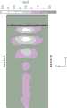
图1a-图1b示出了根据实施例的光学谐振器系统100的示意图。图1a示出了根据实施例的光学谐振器系统100的示意性平面图,并且图1b示出了根据实施例的光学谐振器系统100的示意性截面图。Figures 1a-1b show a schematic diagram of an
如图1a-图1b所示,光学谐振器系统100包括多条波导结构120、STP谐振结构140(STP=板状等离子体激元极化子)和光耦合结构160。As shown in FIGS. 1 a - 1 b , the
多条波导结构120包括用于引导IR辐射RIR的多个间隔开的半导体条122-1、……、122-n(122-#)。在图1a中,多条波导结构120被示例性地示出为包括三个间隔开的(完整的)半导体条122-1、122-2、122-3,其中间隔开的半导体条122-1、……、122-n的数目“n”可以在50至200之间,或在100至140之间,或为(大约)120,例如,当考虑示例性波导宽度(=n×w,其中w=半导体条带的宽度)在100μm至300μm之间,在150μm至250μm之间,或为(大约)200μm。间隔开的半导体条122-1、……、122-n可以通过介电带124(例如,气隙或氧化物)分开。The plurality of
STP谐振结构140包括半导体条142-1、……、142-m和中间介电条144-1、……、144-p(例如,气隙或氧化物)的交替布置,并且包括在STP谐振结构140的边界区域140-1处与半导体条142-m(=图1a-图1b中的142-2)相邻的金属条146。The STP
在图1a-图1b中,STP谐振结构140被示例性地示出为包括两个半导体条142-1、142-2,即,间隔开的半导体条142-1、……、142-m的数目“m”例如可以是2。在图1a-图1b中,STP谐振结构140被示例性地示出为包括两个介电条144-1、144-2,即,间隔开的介电条144-1、……、144-p的数目“p”可以是2,例如(m=p)。数目m、p通常不会由于物理原因而变化,其中条带142-1、142-2、144-1、144-2的宽度(精确地)个体地限定的,如下所述。In FIGS. 1a-1b, the STP
金属条146和相邻半导体条142-m(图1a-图1b中的142-2)被布置为在STP谐振结构140的边界区域140-1处提供金属半导体界面146-A,其中多条波导结构120的半导体条122-1、……、122-n和STP谐振结构140的半导体条142-1、……、142-m被布置为在公共系统平面(=x-z平面)中彼此垂直。
光耦合结构160包括半导体层162,其中半导体层162布置在多条波导结构120与STP谐振结构140之间以将IR辐射RIR光耦合在多条波导结构120与STP谐振结构140之间。The
根据一个实施例,STP谐振结构140可以被实现为在系统平面中横向延伸的布拉格镜结构。根据一个实施例,多条波导结构120的半导体材料、STP谐振结构140的半导体材料和耦合结构160的半导体材料可以包括半导体材料,例如,具有硅或多晶硅材料的基层110,该半导体材料被施加在基板或基板结构180(参见图1b)的第一主表面区域180-A上,第一主表面区域180-A提供光学谐振器系统100的系统平面。According to one embodiment, the STP
如图1b所示,基板(或基板结构)180可以包括多个层,例如,第一绝缘(=介电)层182、第二绝缘(=介电)层184和(可选地)半导体基板层186。第一介电层182可以包括氮化物材料,例如SiN,第二介电层184可以包括氧化物材料,例如BOX=掩埋氧化物(诸如SiO)或空气,并且半导体基板层186可以包括硅。因此,第一介电层182的第一主表面区域形成基板180的顶部主表面区域180-A,即,公共系统平面(=x-z平面)。如图1b所示,基板结构180包括竖直地低于在STP谐振结构140的边界区域140-1处的金属半导体界面146-A的腔188。腔188在基板结构180中形成在STP谐振结构140的边界区域140-1处的金属半导体界面146-A下方减少了从金属半导体界面146-A到相邻材料的热传递。As shown in Fig. 1b, the substrate (or substrate structure) 180 may comprise a plurality of layers, for example a first insulating (=dielectric)
第一绝缘层182可以包括50nm至500nm、100nm至200nm或约140nm的厚度。第二绝缘层114可以包括500nm至5000nm、1500nm至2500nm或约2000nm的厚度。半导体层186可以包括50nm至500nm、100nm至220nm或约160nm的厚度。The first insulating
光学谐振器系统100的原理基于激发所谓的Tamm等离子体激元,其可以作为光学谐振出现在布拉格镜140与金属146之间的边界(界面)146-A处。通常,布拉格镜142-#(142-1、……、142-m)、144-#(144-1、……、144-p)和金属146(即,Tamm等离子(TP)结构140)是用扩展的一维层构建的。如果布拉格镜140和金属146彼此调谐和调节,则谐振波长λRES(在布拉格镜140一侧)的垂直入射光将被场的谐振提升(质量因子)完全吸收。如果假定电介质几乎没有损耗,则金属的固有损耗最终会导致完全吸收。布拉格镜140和金属146的这种调谐(或匹配)是指分别分配给布拉格镜和金属的个体幅度反射系数。例如,如果使用钨W,则在设计中考虑这种匹配,如下所述。如果使用其他金属,则谐振吸收也是可能的(例如,具有不同或更低的性能)。此外,该设计还可以针对其他金属进行调谐和优化。The principle of the
因此,本公开的核心是光学谐振器系统100,其起点是例如由多晶硅制成的介电层波导120。该谐振器系统100在图1a(上部区域)和图1b(中央区域)中描绘。这里,TP结构140的层不再在二维(平行于x-y平面)上(近似)无限延伸,而是(竖直地)受到(多晶硅)层的高度h(y方向,参见图1b)的限制。布拉格镜140(=交替的折射率区域142-#、144-#)可以通过完全去除(例如,通过蚀刻到膜182)多晶硅层(=基层110)的个体矩形面或区域(在纵向截面中)来实现或产生。多晶硅层110的延伸及其对平面的蚀刻可以被认为是无限的。紧邻布拉格镜140,需要与多晶硅层110大约相同高度的金属层146。金属层146可以包括稳定的对温度不敏感的金属,诸如W(钨)、Ag(银)、Mo(钼)等。原则上,金属区域/层146的延伸可以被选择为任何大小。出于与热流有关的原因,仅必须考虑与膜180表面的关系。由于没有光透过金属,因此从光学角度来看,金属条的宽度可以任意选择。因此其可以被选择以便于制造和散热方面。例如,在最佳情况下,金属条的高度可以等于多晶硅(例如,金属层146的高度=多晶硅层(基层)110”的高度)。Thus, the core of the present disclosure is an
因此,金属半导体界面146-A(例如,钨/硅界面)可以在一个位置处实现/生产。该边界层(界面)146-A对于“板状等离子体激元极化子”(STP)结构(或层状等离子体激元极化子)140是必不可少的。建模现在面对的是导层模式,而不是扩展平面波,其中光的包含受硅(例如,多晶硅)的高折射率影响。与一维TP结构相比,STP谐振结构140的结果是,在光学谐振的情况下,存在进入空间的辐射损失,并且该谐振只能针对特定极化进行,即,当电场平行于基板表面时,即,是横向极化(TE极化)或s极化。因此,STP谐振结构140提供远离谐振波长和TE极化的(场)抑制,其中等离子体谐振中场的增加(提升)导致谐振波长和TE极化处发射/吸收的增加。Thus, a metal-semiconductor interface 146-A (eg, a tungsten/silicon interface) can be realized/produced at one location. This boundary layer (interface) 146 -A is essential for the “slab plasmon polaritons” (STP) structure (or layered plasmonic polaritons) 140 . Modeling now deals with guided layer modes rather than extended plane waves, where the inclusion of light is affected by the high refractive index of silicon (eg, polysilicon). The consequence of the STP
到目前为止,仅描述了STP谐振结构140,其为纯二维层结构(在其平面外无限延伸)。为了完成波导吸收器系统100,STP结构140耦合到周期性条波导(多条波导,参见图1a的下部区域)120。通过以周期性间隔将限定宽度的完整连续间隙蚀刻到多晶硅的平板波导(平面波导)中或蚀刻到基层110(例如,硅或多晶硅层)中(以周期性间隔),多条波导120可以以廉价方式制造。上述类型的波导120在灵敏度方面表现出优异的特性(通过模拟和实验)。多条波导结构120与STP谐振结构140的耦合通过光耦合结构160来实现,例如,在STP结构140与多条波导120之间的多晶硅层(具有优化的横向延伸部)的形式。优化的横向延伸部可以从半经验优化中推导出来。通过模拟(由发明人)发现,考虑到平板波导和被耦合的多条波导模式,优化的横向延伸部可以大约对应于平均四分之一波长厚度的五倍。So far only the STP
完整的波导吸收器系统100通过有限元法用三维周期性晶胞(=模拟晶胞)模拟。三维周期性晶胞在图1a-图1b中示例性地示出。The complete
例如,光学谐振器结构100的STP谐振结构140的所得到的谐振波长范围(目标波长)λRES可以在4.15μm至4.35μm之间的范围内选择。For example, the resulting resonance wavelength range (target wavelength) λRES of the STP
对于在4.15μm至4.35μm之间的STP谐振结构140的所得到的谐振波长范围(目标波长)λRES,多条波导结构120的半导体条带122-#可以具有1.3μm至1.5μm的宽度w、0.9μm至1.1μm的高度h和0.25μm至0.35μm的间距(间隙)g。根据一个实施例,多条波导结构120的半导体条122-#可以具有1.4μm的宽度w、1μm的高度h和0.3μm的间距g。For the resulting resonant wavelength range (target wavelength) λRES of the STP
因此,在STP谐振结构140的边界区域140-1处,半导体条142-m(=图1a-图1b中的142-2)可以具有1.0μm至1.15μm的宽度d4和0.9μm至1.1μm的高度h。根据一个实施例,在边界区域140-1处,半导体条142-m(=图1a-图1b中的142-2)可以具有1.07μm的宽度d4和1μm的高度h。STP谐振结构140的另外的半导体条142-#(=图1a-图1b中的142-1)可以具有0.35μm至0.45μm的宽度d2、0.9μm至1.1μm的高度h和0.5μm至0.6μm的间距d1、d3(d1Air、d3Air)。根据一个实施例,STP谐振结构140的另外的半导体条142-#(=图1a-图1b中的142-1)可以具有0.4μm的宽度d2、1μm的高度h和0.55μm的间距d1、d3(d1Air、d3Air)。Therefore, at the boundary region 140-1 of the STP
根据一个实施例,耦合结构160的半导体层162可以具有1.7μm至2.1μm的长度d0和0.9μm至1.1μm的高度h。根据一个实施例,耦合结构160的半导体层162可以具有1.9μm的长度d0和1μm的高度h。According to an embodiment, the
原则上,上述尺寸的缩放对于实现光学谐振器结构100的STP谐振结构140的不同结果谐振波长范围(目标波长)λRES是可能的。然而,应当记住,Si的本征吸收在波长λ>6μm时占主导地位。In principle, scaling of the dimensions described above is possible for realizing different resulting resonance wavelength ranges (target wavelengths) λRES of the STP
根据一个实施例,多条波导结构120包括用于引导IR辐射RIR的平板模式的多个平板波导122-1、……、122-n。According to one embodiment, the plurality of
图2示出了根据实施例的窄带中红外辐射源200的示意性俯视图。窄带中红外辐射源200包括如上文关于图1a-图1b描述的光学谐振器系统100、以及用于向STP谐振结构140发射宽带红外辐射RIR的红外辐射发射器220,其中在STP谐振结构140的谐振波长范围λRES内的IR辐射RIR从STP谐振结构140传播到光耦合结构160并且耦合到多条波导结构120中。Fig. 2 shows a schematic top view of a narrowband
根据一个实施例,STP谐振结构140被配置为滤光结构,该滤光结构用于对由红外辐射发射器220发射的宽带红外辐射RIR进行过滤并且根据STP谐振结构140的谐振波长范围λRES提供IR辐射R'IR作为具有中心波长λ0的已过滤红外辐射。According to one embodiment, the STP
根据一个实施例,多条波导结构120被配置为引导具有中心波长λ0的(已过滤的)IR辐射R'IR,其中被引导的IR辐射R'IR(=由多条波导结构引导的已过滤的IR辐射)包括用于与周围大气相互作用的倏逝场(evanescent field)分量。According to one embodiment, the
根据一个实施例,耦合结构160被配置为将具有中心波长λ0的IR辐射的模式耦合到多条波导结构中。According to one embodiment, the
根据一个实施例,在STP谐振结构140的边界区域140-1处与半导体条142-2相邻的金属条146可以(可选地)被布置为形成加热元件,即,红外辐射发射器220。因此,金属(例如,Ag、W、Mo、……)146可以接触,以便通过施加电压生成焦耳热。According to one embodiment, the
根据另一(可选)实施例,可以可选地提供独立的(隔离的)高n掺杂的多晶硅线222作为加热元件(热辐射发射器)220,其发射与普朗克辐射定律成比例的宽带IR辐射RIR。n掺杂的多晶硅线可以在Si/W边界146-1附近被加热,如图2中可选地描绘的。According to another (optional) embodiment, a separate (isolated) highly n-doped polysilicon line 222 may optionally be provided as a heating element (thermal radiation emitter) 220, the emission of which is proportional to Planck's radiation law The broadband IR radiation RIR . The n-doped polysilicon line may be heated near the Si/W boundary 146 - 1 , as optionally depicted in FIG. 2 .
加热元件220(可选地为金属条146的形式或为掺杂的多晶硅线222的形式)可以被配置为在致动条件下具有在600K至1000K之间或600K至700K之间的范围内的操作温度。在金属条146的致动条件下,金属条146连接到电压源VM。在多晶硅线222的致动条件下,多晶硅线222连接到电压源VSi。根据一个实施例,红外辐射发射器连接到电源240,电源240用于提供电能以使红外辐射发射器处于致动条件。The heating element 220 (optionally in the form of a
图3示出了根据实施例的流体传感器300的示例性示意图。根据一个实施例,流体传感器300包括如上文关于图2描述的窄带中红外辐射源200、以及中红外辐射检测器320,中红外辐射检测器320被配置为基于从多条波导结构120接收的被引导的(和已过滤的)红外辐射(=红外光波)R'IR的强度来提供检测器输出信号。FIG. 3 shows an exemplary schematic diagram of a
根据一个实施例,中红外辐射检测器可以包括热电堆结构,其中中红外辐射检测器被配置为感测入射的被引导的红外辐射,入射的被引导的红外辐射是基于受目标流体FT影响的倏逝场吸收对周围大气中目标流体FT的浓度的量度。倏逝场分量与周围大气中的目标流体的相互作用导致透射的IR辐射由于吸收而(由多条波导120在发射器200与检测器300之间透射的被引导的红外辐射)减少,该吸收是测量周围大气中目标流体浓度的量度。According to one embodiment, the mid-infrared radiation detector may comprise a thermopile structure, wherein the mid-infrared radiation detector is configured to sense incident guided infrared radiation based on the influence of the target fluidFT The evanescent field absorption is a measure of the concentration of the target fluidFT in the surrounding atmosphere. The interaction of the evanescent field component with the target fluid in the surrounding atmosphere results in a reduction of the transmitted IR radiation (guided infrared radiation transmitted by the plurality of
根据另一实施例,中红外辐射检测器可以包括热释电温度传感器、压电温度传感器、pn结温度传感器和电阻温度传感器中的至少一种。According to another embodiment, the mid-infrared radiation detector may include at least one of a pyroelectric temperature sensor, a piezoelectric temperature sensor, a pn junction temperature sensor, and a resistive temperature sensor.
由波导120引导的已过滤的IR辐射包括用于与具有目标流体的周围大气相互作用的倏逝场分量,其中倏逝场分量与周围大气的相互作用导致透射的热辐射R'IR由于被引导的辐射R'IR的吸收而减少,该吸收是周围大气或介质中目标流体浓度的量度。因此,流体传感器300可以提供CMOS MID IR气体和液体传感器,该传感器用于利用如上文关于图2描述的窄带中红外辐射源200和中红外辐射检测器320基于叠加倏逝场的形成来感测周围大气或介质中的目标流体浓度(例如,CO/CO2/O3/NOx/甲烷)。The filtered IR radiation guided by
在本文中,术语流体可以涉及液体或气体。在环境介质涉及环境空气的情况下,目标流体可以涉及存在于环境空气中的目标气体或目标气体组分。本概念同样适用于感测环境介质中的目标液体或目标液体组分。In this context, the term fluid may refer to liquids or gases. Where the ambient medium is ambient air, the target fluid may be a target gas or a target gas component present in the ambient air. The concept is equally applicable to sensing target liquids or target liquid components in ambient media.
图4a示出了根据实施例的具有热电堆结构的中红外辐射检测器320的示意性截面图。图4b示出了根据实施例的具有热电堆结构320'的中红外辐射检测器320的示意性截面图。Fig. 4a shows a schematic cross-sectional view of a
中红外辐射检测器320可以布置在具有多个层182、184和(可选地)186的基板(或基板结构)180上。如图4b所示,基板结构180包括竖直地低于在热电堆结构的另外的腔388。在基板结构180中形成腔388可以减少从热电堆结构320'到相邻材料的热传递。热电堆结构包括多个交替掺杂(磷和硼)的Si条带322-1、322-2,它们通过金属触点324电连接以提供连接的金属条322-1、322-2的曲折形式。A
在热电堆结构320'的输入部分(与波导120相邻)处,辐射检测器320包括半导体条326和中间介电条328(例如,气隙或氧化物),的交替布置并且包括在热电堆结构320'的边界区域320-1处与半导体条326相邻的金属条330。半导体条326和中间介电条328的交替布置横向地夹在(半导体)区域120与金属330之间。At the input portion of the thermopile structure 320' (adjacent to the waveguide 120), the
中红外辐射检测器320形成谐振吸收器,谐振吸收器提供波长选择性吸收并且随后提供选择性热生成。由于金属330是吸收性元素,所以热生成的中心会在那里。这导致热电堆结构320'的左侧与右侧之间的温度差。条带332(例如,二氧化硅(SiO2)条)的目的是与金属触点324的电绝缘,同时保持与掺杂的Si条322-1、322-2的紧密热接触。半导体区域334(Si平板)的目的是与基板180的热接触。因此,为了使左右两侧的温度差最大化,金属330和紧邻热电堆结构320'的条带332应当尽可能窄,而半导体区域334的范围可以形成热设计的优化参数(取决于膜尺寸、掺杂条带的热导率等)并且最终可以等于0。The
为了测量透射的热辐射R'IR的选择性检测和谐振吸收,可以使用热电堆来实现,如图4a-图4b所示。选择性吸收确保了在Si/金属边界层的区域中选择性加热。通过交替掺杂(磷和硼)的Si条带的对应接触,当谐振波长被STP谐振结构140接触,即,从STP谐振结构140通过多条波导120透射到中红外辐射检测器220时,Seebeck效应可以生成(可检测)电压V。在图4a-图4b中,用非常高掺杂的多晶硅(例如,接近溶解度极限的磷掺杂浓度(约1021cm-3))代替金属(金属触点)也是可能和可行的。To measure the selective detection and resonant absorption of the transmitted thermal radiationR'IR , a thermopile can be used, as shown in Figure 4a–4b. Selective absorption ensures selective heating in the region of the Si/metal boundary layer. By corresponding contacts of alternately doped (phosphorous and boron) Si strips, when the resonant wavelength is contacted by the STP
根据一个实施例,基板包括竖直地低于在红外辐射发射器和中红外辐射检测器中的至少一项的腔。According to one embodiment, the substrate includes a cavity vertically below at least one of the infrared radiation emitter and the mid-infrared radiation detector.
在热辐射发射器120下方和可选地在热辐射检测器320下方的基板结构180中的腔188、388的形成减少了从热辐射发射器120和/或热辐射检测器320到相邻材料中的热传递,因此可以提高热辐射发射器的发射效率以及热辐射检测器的检测效率。The formation of
图5a-图5c示出了(a)多条波导的入射模式场(也表示对应感测应用的WG模式(WG=波导)),(b)波导吸收器系统在谐振时的场分布(俯视图),以及(c)纵向(横截面)视图中谐振时的场分布。Figures 5a-5c show (a) the incident mode field for multiple waveguides (also denoting the WG mode for sensing applications (WG = waveguide)), (b) the field distribution of the waveguide absorber system at resonance (top view ), and (c) the field distribution at resonance in the longitudinal (cross-sectional) view.
图6a-图6b示出了根据实施例的对于(a)氮化物膜下方的空气和(b)氮化物膜下方的氧化物的多晶硅层的不同高度的选择性吸收。Figures 6a-6b illustrate selective absorption for different heights of the polysilicon layer for (a) air below the nitride film and (b) oxide below the nitride film, according to an embodiment.
图7示出了(以表格形式)不同基板材料(空气/氧化物)和SI层厚度h(“包含因子倏逝场γ、波导自衰减α、谐振时的频谱发射率ε(λr)和谐振的Q因子”)的结果概述。Figure 7 shows (in tabular form) the spectral emissivity ε(λ r ) at resonance for different substrate materials (air/oxide) and SI layer thicknesses h ("inclusion factors evanescent field γ, waveguide self-attenuation α, spectral emissivity ε(λr ) and Oscillating Q-factor”) results overview.
图5b-图5c只是演示了模拟的相对场增强,这进而又是这种谐振传感器相对于具有宽带源的传感器的检测极限的可能改进的量度。图6和图7也是如此,它们突出显示了多晶硅厚度对性能的影响。Figures 5b-5c merely demonstrate the simulated relative field enhancement, which in turn is a measure of the possible improvement in the detection limit of such a resonant sensor relative to a sensor with a broadband source. The same is true for Figures 6 and 7, which highlight the effect of polysilicon thickness on performance.
描述了可以单独使用或与本文中描述的特征和功能组合使用的附加实施例和方面。Additional embodiments and aspects are described which can be used alone or in combination with the features and functions described herein.
根据一个实施例,一种光学谐振器系统包括多条波导结构、STP谐振结构(STP=板状等离子体激元极化子)和光耦合结构。According to one embodiment, an optical resonator system comprises a plurality of waveguide structures, an STP resonator structure (STP = slab plasmon polaritons) and an optical coupling structure.
所述多条波导结构包括用于引导IR辐射的多个间隔开的半导体条。所述STP谐振结构包括半导体条和中间介电条的交替布置并且包括在所述STP谐振结构的边界区域处与所述半导体条相邻的金属条。所述金属条和所述相邻半导体条被布置为在所述STP谐振结构的所述边界区域处提供金属半导体界面,其中所述多条波导结构的所述半导体条和所述STP谐振结构的所述半导体条被布置为在公共系统平面中彼此垂直。所述光耦合结构具有半导体层,其中所述半导体层布置在所述多条波导结构与所述STP谐振结构之间以将所述IR辐射光耦合在所述多条波导结构与所述STP谐振结构之间。The plurality of waveguide structures includes a plurality of spaced apart semiconductor strips for guiding IR radiation. The STP resonant structure includes an alternating arrangement of semiconductor strips and intermediate dielectric strips and includes metal strips adjacent to the semiconductor strips at border regions of the STP resonant structure. The metal strip and the adjacent semiconductor strips are arranged to provide a metal-semiconductor interface at the boundary region of the STP resonant structure, wherein the semiconductor strips of the plurality of waveguide structures and the STP resonant structure The semiconductor strips are arranged perpendicular to each other in a common system plane. The optical coupling structure has a semiconductor layer, wherein the semiconductor layer is disposed between the plurality of waveguide structures and the STP resonant structure to optically couple the IR radiation between the plurality of waveguide structures and the STP resonant structure between structures.
根据一个实施例,所述STP谐振结构被实现为在所述系统平面中横向延伸的布拉格镜结构。According to one embodiment, the STP resonant structure is realized as a Bragg mirror structure extending laterally in the system plane.
根据一个实施例,所述多条波导结构的半导体材料、所述STP结构的半导体材料和所述耦合结构的半导体材料可以包括半导体材料,例如硅或多晶硅材料,所述半导体材料被施加在基板的第一主表面区域上,所述第一主表面区域提供所述光学谐振器系统的所述系统平面。According to an embodiment, the semiconductor material of the plurality of waveguide structures, the semiconductor material of the STP structure and the semiconductor material of the coupling structure may include semiconductor materials, such as silicon or polysilicon materials, and the semiconductor materials are applied on the substrate. On a first major surface region, said first major surface region provides said system plane of said optical resonator system.
根据一个实施例,所述多条波导结构的所述半导体条具有1.3μm至1.5μm的宽度、0.9μm至1.1μm的高度和0.25μm至0.35μm的间距,并且特别地具有1.4μm的宽度、1μm的高度和0.3μm的间距。According to one embodiment, said semiconductor strips of said plurality of waveguide structures have a width of 1.3 μm to 1.5 μm, a height of 0.9 μm to 1.1 μm and a pitch of 0.25 μm to 0.35 μm, and in particular a width of 1.4 μm, 1 μm height and 0.3 μm pitch.
根据一个实施例,在所述STP谐振结构的所述边界区域处,所述半导体条带具有1.0μm至1.15μm的宽度和0.9μm至1.1μm的高度,并且特别地具有1.07μm的宽度和1μm的高度,其中所述STP谐振结构的另外的半导体条具有0.3μm5至0.45μm的宽度、0.9μm至1.1μm的高度和0.5μm至0.6μm的间距,并且特别地具有0.4μm的宽度、1μm的高度和0.55μm的间距。According to one embodiment, at the border region of the STP resonant structure, the semiconductor strip has a width of 1.0 μm to 1.15 μm and a height of 0.9 μm to 1.1 μm, and in particular a width of 1.07 μm and a height of 1 μm , wherein the further semiconductor strips of the STP resonant structure have a width of 0.3 μm5 to 0.45 μm, a height of 0.9 μm to 1.1 μm and a pitch of 0.5 μm to 0.6 μm, and in particular a width of 0.4 μm, a width of 1 μm height and pitch of 0.55µm.
根据一个实施例,所述耦合结构的所述半导体层具有1.7μm至2.1μm的长度和0.9μm至1.1μm的高度,并且特别地具有1.9μm的长度和1μm的高度。According to one embodiment, the semiconductor layer of the coupling structure has a length of 1.7 μm to 2.1 μm and a height of 0.9 μm to 1.1 μm, and in particular a length of 1.9 μm and a height of 1 μm.
根据一个实施例,所述多条波导结构包括用于引导所述IR辐射的平板模式的多个平板波导。According to one embodiment, said plurality of waveguide structures comprises a plurality of slab waveguides for guiding slab modes of said IR radiation.
根据一个实施例,一种窄带中红外辐射源包括所述光学谐振器系统;以及用于向所述STP谐振结构发射宽带红外辐射的红外辐射发射器,其中在所述STP谐振结构的所述谐振波长范围内的所述IR辐射从所述STP谐振结构传播到所述光耦合结构并且耦合到所述多条波导结构中。According to one embodiment, a source of narrow-band mid-infrared radiation comprises said optical resonator system; and an infrared radiation emitter for emitting broadband infrared radiation to said STP resonant structure, wherein said resonator in said STP resonant structure The IR radiation in the wavelength range propagates from the STP resonant structure to the optical coupling structure and is coupled into the plurality of waveguide structures.
根据一个实施例,所述STP结构被配置为滤光结构,所述滤光结构用于对由所述红外辐射发射器发射的所述宽带红外辐射进行过滤并且根据所述STP谐振结构的所述谐振波长范围提供所述IR辐射作为具有中心波长的已过滤红外辐射。According to an embodiment, the STP structure is configured as a filter structure for filtering the broadband infrared radiation emitted by the infrared radiation emitter and according to the The resonant wavelength range provides said IR radiation as filtered infrared radiation having a central wavelength.
根据一个实施例,所述多条波导结构被配置为引导具有所述中心波长的(已过滤的)IR辐射,其中被引导的IR辐射(由所述多条波导结构引导的所述已过滤的IR辐射)包括用于与周围大气相互作用的倏逝场分量。According to one embodiment, said plurality of waveguide structures is configured to guide (filtered) IR radiation having said central wavelength, wherein the guided IR radiation (the filtered IR radiation guided by said plurality of waveguide structures IR radiation) includes an evanescent field component for interaction with the surrounding atmosphere.
根据一个实施例,所述耦合结构被配置为将具有所述中心波长的所述IR辐射的模式耦合到所述多条波导结构中。According to one embodiment, said coupling structure is configured to couple a mode of said IR radiation having said central wavelength into said plurality of waveguide structures.
根据一个实施例,在所述STP谐振结构的所述边界区域处与所述半导体条相邻的所述金属条被布置为形成加热元件并且被配置为在致动条件下具有在600K至1000K之间或600K至700K之间的范围内的操作温度,并且其中所述红外辐射发射器连接到电源,所述电源用于提供电能以使所述红外辐射发射器处于所述致动条件。According to one embodiment, said metal strip adjacent to said semiconductor strip at said boundary region of said STP resonant structure is arranged to form a heating element and is configured to have a temperature between 600K and 1000K under actuated conditions. An operating temperature in the range between 600K and 700K, and wherein said infrared radiation emitter is connected to a power source for providing electrical energy to place said infrared radiation emitter in said actuated condition.
根据一个实施例,一种流体传感器包括所述窄带中红外辐射源和中红外辐射检测器,所述中红外辐射检测器被配置为基于从所述多条波导结构接收的所述被引导的(和已过滤的)红外辐射(=红外光波)的强度来提供检测器输出信号。According to one embodiment, a fluid sensor includes said source of narrow-band mid-infrared radiation and a detector of mid-infrared radiation configured to be based on said guided ( and filtered) infrared radiation (=infrared light waves) to provide the detector output signal.
根据一个实施例,所述中红外辐射检测器包括热电堆结构,其中所述中红外辐射检测器被配置为感测入射的被引导的红外辐射,所述入射的被引导的红外辐射是基于受目标流体影响的所述倏逝场吸收对所述周围大气中所述目标流体的浓度的量度,其中所述倏逝场分量与所述周围大气中的所述目标流体的相互作用导致透射的IR辐射由于吸收而(由所述多条波导传输的被引导的红外辐射)减少,所述吸收是所述周围大气中所述目标流体浓度的量度。According to one embodiment, the mid-infrared radiation detector comprises a thermopile structure, wherein the mid-infrared radiation detector is configured to sense incident guided infrared radiation based on the detected The evanescent field absorption influenced by the target fluid is a measure of the concentration of the target fluid in the surrounding atmosphere, wherein the interaction of the evanescent field component with the target fluid in the surrounding atmosphere results in a transmitted IR Radiation is reduced (guided infrared radiation transmitted by the plurality of waveguides) due to absorption, which is a measure of the target fluid concentration in the surrounding atmosphere.
根据一个实施例,所述基板包括竖直地低于在所述红外辐射发射器和所述中红外辐射检测器中的至少一项的腔。According to one embodiment, said substrate comprises a cavity vertically below at least one of said infrared radiation emitter and said mid-infrared radiation detector.
描述了可以单独使用或与本文中描述的特征和功能组合使用的附加实施例和方面。Additional embodiments and aspects are described which can be used alone or in combination with the features and functions described herein.
尽管一些方面已经在装置的上下文中被描述为特征,但显然这种描述也可以被视为对方法的对应特征的描述。尽管某些方面已经在方法的上下文中被描述为特征,但显然这种描述也可以被视为对与装置的功能相关的对应特征的描述。Although some aspects have been described as features in the context of an apparatus, it will be apparent that this description can also be considered a description of corresponding features of the method. Although certain aspects have been described as features in the context of a method, it will be apparent that this description may also be considered a description of corresponding features in relation to the functionality of the apparatus.
取决于某些实现要求,控制电路系统的实施例可以以硬件或软件或至少部分以硬件或至少部分以软件实现。通常,控制电路系统的实施例可以实现为具有程序代码的计算机程序产品,当计算机程序产品在计算机上运行时,该程序代码可操作用于执行方法中的一个。程序代码可以例如存储在机器可读载体上。Depending on certain implementation requirements, embodiments of the control circuitry may be implemented in hardware or software or at least partly in hardware or at least partly in software. In general, embodiments of the control circuitry may be implemented as a computer program product having a program code operable to perform one of the methods when the computer program product is run on a computer. The program code may eg be stored on a machine readable carrier.
在前面的详细描述中,可以看出,为了简化本公开的目的,在示例中将各种特征组合在一起。该公开方法不应当被解释为反映所要求保护的示例需要比每个权利要求中明确列举的更多特征的意图。相反,如所附权利要求所反映的,主题可能不在于单个公开示例的所有特征。因此,所附权利要求在此并入详细描述中,其中每个权利要求可以作为单独的示例独立存在。虽然每个权利要求可以作为单独的示例独立存在,但应当注意,尽管从属权利要求在权利要求中可能涉及与一个或多个其他权利要求的特定组合,但其他示例也可以包括从属权利要求与每个其他从属权利要求的主题的组合或每个特征与其他从属或独立权利要求的组合。这样的组合在本文中提出了,除非声明不打算使用特定组合。此外,旨在将权利要求的特征包括在任何其他独立权利要求中,即使该权利要求不直接依赖于该独立权利要求。In the foregoing Detailed Description, it can be seen that various features are grouped together in examples for the purpose of streamlining the disclosure. This method of disclosure is not to be interpreted as reflecting an intention that the claimed examples require more features than are expressly recited in each claim. Rather, as the following claims reflect, subject matter may lie in less than all features of a single disclosed example. Thus the following claims are hereby incorporated into the Detailed Description, with each claim standing on its own as a separate example. While each claim may stand on its own as a separate example, it should be noted that although a dependent claim may refer to a particular combination with one or more other claims within a claim, other examples may also include a dependent claim in conjunction with each subject matter of each of the other dependent claims or each feature in combination with other dependent or independent claims. Such combinations are proposed herein unless it is stated that a particular combination is not intended to be used. Furthermore, it is intended to include features of a claim in any other independent claim, even if that claim is not directly dependent on this independent claim.
尽管本文中已经说明和描述了特定实施例,但是本领域普通技术人员将理解,在不脱离本实施例的范围的情况下,所示出和描述的特定实施例可以用各种替代和/或等效实现代替。本申请旨在涵盖本文中讨论的特定实施例的任何修改或变化。因此,实施例旨在仅由权利要求及其等同物来限制。Although specific embodiments have been illustrated and described herein, those of ordinary skill in the art will appreciate that various substitutions and/or Equivalent implementations are substituted. This application is intended to cover any adaptations or variations of the specific embodiments discussed herein. Accordingly, it is intended that the embodiments be limited only by the claims and the equivalents thereof.
Claims (15)
Translated fromChineseApplications Claiming Priority (2)
| Application Number | Priority Date | Filing Date | Title |
|---|---|---|---|
| EP21204001.8AEP4170321B1 (en) | 2021-10-21 | 2021-10-21 | Optical resonator system, narrowband mid-infrared radiation source and fluid sensor |
| EP21204001.8 | 2021-10-21 |
Publications (1)
| Publication Number | Publication Date |
|---|---|
| CN116009146Atrue CN116009146A (en) | 2023-04-25 |
Family
ID=78371853
Family Applications (1)
| Application Number | Title | Priority Date | Filing Date |
|---|---|---|---|
| CN202211292650.9APendingCN116009146A (en) | 2021-10-21 | 2022-10-20 | Optical resonator system, narrowband mid-infrared radiation source and fluid sensor |
Country Status (3)
| Country | Link |
|---|---|
| US (1) | US12050340B2 (en) |
| EP (1) | EP4170321B1 (en) |
| CN (1) | CN116009146A (en) |
Families Citing this family (1)
| Publication number | Priority date | Publication date | Assignee | Title |
|---|---|---|---|---|
| CN119556491B (en)* | 2024-11-19 | 2025-09-16 | 华中科技大学 | A passive coherent long-wave infrared radiation sensing photonic integrated device |
Family Cites Families (5)
| Publication number | Priority date | Publication date | Assignee | Title |
|---|---|---|---|---|
| FR2965665B1 (en)* | 2010-09-30 | 2012-10-26 | Centre Nat Rech Scient | SOURCES AND LIGHT SENSORS COMPRISING AT LEAST ONE LOCALIZED PLASMONIC TAMM MODE MICROCAVITY |
| JP6994274B2 (en)* | 2018-05-25 | 2022-02-04 | 国立研究開発法人物質・材料研究機構 | Stacked radiant light source |
| EP3705872B1 (en)* | 2019-03-08 | 2025-07-09 | Infineon Technologies AG | Gas sensor |
| EP3715829B9 (en)* | 2019-03-27 | 2022-06-22 | Infineon Technologies AG | Fluid sensor and method for manufacturing a fluid sensor |
| WO2022192570A1 (en)* | 2021-03-10 | 2022-09-15 | Atomos Nuclear and Space Corporation | System and method for converting and transmitting energy |
- 2021
- 2021-10-21EPEP21204001.8Apatent/EP4170321B1/enactiveActive
- 2022
- 2022-10-13USUS18/046,231patent/US12050340B2/enactiveActive
- 2022-10-20CNCN202211292650.9Apatent/CN116009146A/enactivePending
Also Published As
| Publication number | Publication date |
|---|---|
| US12050340B2 (en) | 2024-07-30 |
| US20230125167A1 (en) | 2023-04-27 |
| EP4170321B1 (en) | 2025-01-29 |
| EP4170321A1 (en) | 2023-04-26 |
Similar Documents
| Publication | Publication Date | Title |
|---|---|---|
| US10598590B2 (en) | Sensor device and a method of detecting a component in gas | |
| US20160103341A1 (en) | Actively Tunable Polar-Dielectric Optical Devices | |
| CN111665211B (en) | Gas Sensors | |
| US11506599B2 (en) | Fluid sensor including an optical filter and a waveguide, and method for manufacturing the fluid sensor | |
| US9372114B2 (en) | Spectrophotometer comprising an integrated Fabry-Perot interferometer | |
| US20180374981A1 (en) | Metamaterial Thermal Pixel for Limited Bandwidth Electromagnetic Sourcing and Detection | |
| CN103907248A (en) | Thermo-optically tunable laser system | |
| CN103733354B (en) | terahertz detection unit | |
| CN116009146A (en) | Optical resonator system, narrowband mid-infrared radiation source and fluid sensor | |
| Ling et al. | Near-unity light–matter interaction in mid-infrared van der waals metasurfaces | |
| De Luca et al. | Filterless non-dispersive infra-red gas detection: A proof of concept | |
| Negm et al. | Graphene thermal infrared emitters integrated into silicon photonic waveguides | |
| JP6269008B2 (en) | Electromagnetic wave-surface polariton conversion element. | |
| WO2020086004A1 (en) | Thermocouple, thermopile and devices | |
| JP6327349B2 (en) | GAS MEASURING DEVICE, COLLECTIVE SUBSTRATE, ITS MANUFACTURING METHOD, AND INFRARED LIGHT SOURCE AND SENSOR | |
| Wu et al. | Ultracompact on-chip photothermal power monitor based on silicon hybrid plasmonic waveguides | |
| JP4728989B2 (en) | Raman scattering light enhancement device | |
| US11385421B2 (en) | Optical device, gas sensor, methods of forming and operating the same | |
| CN115597714A (en) | Sensor and method for detecting guided thermal radiation | |
| Ishihara et al. | Power efficient microheater for wavelength selective infrared emitter and CO 2 gas sensing | |
| US11073474B2 (en) | Device and method for detecting the presence of determined molecules, and biosensor | |
| JP2024130550A (en) | Optical Semiconductor Devices |
Legal Events
| Date | Code | Title | Description |
|---|---|---|---|
| PB01 | Publication | ||
| PB01 | Publication | ||
| SE01 | Entry into force of request for substantive examination | ||
| SE01 | Entry into force of request for substantive examination |