CN115996575A - Nonvolatile memory device and memory system including the same - Google Patents
Nonvolatile memory device and memory system including the sameDownload PDFInfo
- Publication number
- CN115996575A CN115996575ACN202210996420.4ACN202210996420ACN115996575ACN 115996575 ACN115996575 ACN 115996575ACN 202210996420 ACN202210996420 ACN 202210996420ACN 115996575 ACN115996575 ACN 115996575A
- Authority
- CN
- China
- Prior art keywords
- layer
- insulating
- disposed
- conductive
- etch stop
- Prior art date
- Legal status (The legal status is an assumption and is not a legal conclusion. Google has not performed a legal analysis and makes no representation as to the accuracy of the status listed.)
- Pending
Links
Images


Classifications
- H—ELECTRICITY
- H01—ELECTRIC ELEMENTS
- H01L—SEMICONDUCTOR DEVICES NOT COVERED BY CLASS H10
- H01L25/00—Assemblies consisting of a plurality of semiconductor or other solid state devices
- H01L25/03—Assemblies consisting of a plurality of semiconductor or other solid state devices all the devices being of a type provided for in a single subclass of subclasses H10B, H10D, H10F, H10H, H10K or H10N, e.g. assemblies of rectifier diodes
- H01L25/04—Assemblies consisting of a plurality of semiconductor or other solid state devices all the devices being of a type provided for in a single subclass of subclasses H10B, H10D, H10F, H10H, H10K or H10N, e.g. assemblies of rectifier diodes the devices not having separate containers
- H01L25/065—Assemblies consisting of a plurality of semiconductor or other solid state devices all the devices being of a type provided for in a single subclass of subclasses H10B, H10D, H10F, H10H, H10K or H10N, e.g. assemblies of rectifier diodes the devices not having separate containers the devices being of a type provided for in group H10D89/00
- H01L25/0657—Stacked arrangements of devices
- H—ELECTRICITY
- H10—SEMICONDUCTOR DEVICES; ELECTRIC SOLID-STATE DEVICES NOT OTHERWISE PROVIDED FOR
- H10B—ELECTRONIC MEMORY DEVICES
- H10B43/00—EEPROM devices comprising charge-trapping gate insulators
- H10B43/30—EEPROM devices comprising charge-trapping gate insulators characterised by the memory core region
- H10B43/35—EEPROM devices comprising charge-trapping gate insulators characterised by the memory core region with cell select transistors, e.g. NAND
- H—ELECTRICITY
- H01—ELECTRIC ELEMENTS
- H01L—SEMICONDUCTOR DEVICES NOT COVERED BY CLASS H10
- H01L24/00—Arrangements for connecting or disconnecting semiconductor or solid-state bodies; Methods or apparatus related thereto
- H01L24/01—Means for bonding being attached to, or being formed on, the surface to be connected, e.g. chip-to-package, die-attach, "first-level" interconnects; Manufacturing methods related thereto
- H01L24/02—Bonding areas ; Manufacturing methods related thereto
- H01L24/07—Structure, shape, material or disposition of the bonding areas after the connecting process
- H01L24/08—Structure, shape, material or disposition of the bonding areas after the connecting process of an individual bonding area
- H—ELECTRICITY
- H01—ELECTRIC ELEMENTS
- H01L—SEMICONDUCTOR DEVICES NOT COVERED BY CLASS H10
- H01L24/00—Arrangements for connecting or disconnecting semiconductor or solid-state bodies; Methods or apparatus related thereto
- H01L24/80—Methods for connecting semiconductor or other solid state bodies using means for bonding being attached to, or being formed on, the surface to be connected
- H—ELECTRICITY
- H01—ELECTRIC ELEMENTS
- H01L—SEMICONDUCTOR DEVICES NOT COVERED BY CLASS H10
- H01L25/00—Assemblies consisting of a plurality of semiconductor or other solid state devices
- H01L25/18—Assemblies consisting of a plurality of semiconductor or other solid state devices the devices being of the types provided for in two or more different main groups of the same subclass of H10B, H10D, H10F, H10H, H10K or H10N
- H—ELECTRICITY
- H01—ELECTRIC ELEMENTS
- H01L—SEMICONDUCTOR DEVICES NOT COVERED BY CLASS H10
- H01L25/00—Assemblies consisting of a plurality of semiconductor or other solid state devices
- H01L25/50—Multistep manufacturing processes of assemblies consisting of devices, the devices being individual devices of subclass H10D or integrated devices of class H10
- H—ELECTRICITY
- H10—SEMICONDUCTOR DEVICES; ELECTRIC SOLID-STATE DEVICES NOT OTHERWISE PROVIDED FOR
- H10B—ELECTRONIC MEMORY DEVICES
- H10B43/00—EEPROM devices comprising charge-trapping gate insulators
- H10B43/20—EEPROM devices comprising charge-trapping gate insulators characterised by three-dimensional arrangements, e.g. with cells on different height levels
- H10B43/23—EEPROM devices comprising charge-trapping gate insulators characterised by three-dimensional arrangements, e.g. with cells on different height levels with source and drain on different levels, e.g. with sloping channels
- H10B43/27—EEPROM devices comprising charge-trapping gate insulators characterised by three-dimensional arrangements, e.g. with cells on different height levels with source and drain on different levels, e.g. with sloping channels the channels comprising vertical portions, e.g. U-shaped channels
- H—ELECTRICITY
- H10—SEMICONDUCTOR DEVICES; ELECTRIC SOLID-STATE DEVICES NOT OTHERWISE PROVIDED FOR
- H10B—ELECTRONIC MEMORY DEVICES
- H10B43/00—EEPROM devices comprising charge-trapping gate insulators
- H10B43/40—EEPROM devices comprising charge-trapping gate insulators characterised by the peripheral circuit region
- H—ELECTRICITY
- H10—SEMICONDUCTOR DEVICES; ELECTRIC SOLID-STATE DEVICES NOT OTHERWISE PROVIDED FOR
- H10B—ELECTRONIC MEMORY DEVICES
- H10B43/00—EEPROM devices comprising charge-trapping gate insulators
- H10B43/50—EEPROM devices comprising charge-trapping gate insulators characterised by the boundary region between the core and peripheral circuit regions
- H—ELECTRICITY
- H01—ELECTRIC ELEMENTS
- H01L—SEMICONDUCTOR DEVICES NOT COVERED BY CLASS H10
- H01L2224/00—Indexing scheme for arrangements for connecting or disconnecting semiconductor or solid-state bodies and methods related thereto as covered by H01L24/00
- H01L2224/01—Means for bonding being attached to, or being formed on, the surface to be connected, e.g. chip-to-package, die-attach, "first-level" interconnects; Manufacturing methods related thereto
- H01L2224/02—Bonding areas; Manufacturing methods related thereto
- H01L2224/07—Structure, shape, material or disposition of the bonding areas after the connecting process
- H01L2224/08—Structure, shape, material or disposition of the bonding areas after the connecting process of an individual bonding area
- H01L2224/081—Disposition
- H01L2224/0812—Disposition the bonding area connecting directly to another bonding area, i.e. connectorless bonding, e.g. bumpless bonding
- H01L2224/08135—Disposition the bonding area connecting directly to another bonding area, i.e. connectorless bonding, e.g. bumpless bonding the bonding area connecting between different semiconductor or solid-state bodies, i.e. chip-to-chip
- H01L2224/08145—Disposition the bonding area connecting directly to another bonding area, i.e. connectorless bonding, e.g. bumpless bonding the bonding area connecting between different semiconductor or solid-state bodies, i.e. chip-to-chip the bodies being stacked
- H—ELECTRICITY
- H01—ELECTRIC ELEMENTS
- H01L—SEMICONDUCTOR DEVICES NOT COVERED BY CLASS H10
- H01L2224/00—Indexing scheme for arrangements for connecting or disconnecting semiconductor or solid-state bodies and methods related thereto as covered by H01L24/00
- H01L2224/80—Methods for connecting semiconductor or other solid state bodies using means for bonding being attached to, or being formed on, the surface to be connected
- H01L2224/80001—Methods for connecting semiconductor or other solid state bodies using means for bonding being attached to, or being formed on, the surface to be connected by connecting a bonding area directly to another bonding area, i.e. connectorless bonding, e.g. bumpless bonding
- H01L2224/80003—Methods for connecting semiconductor or other solid state bodies using means for bonding being attached to, or being formed on, the surface to be connected by connecting a bonding area directly to another bonding area, i.e. connectorless bonding, e.g. bumpless bonding involving a temporary auxiliary member not forming part of the bonding apparatus
- H01L2224/80006—Methods for connecting semiconductor or other solid state bodies using means for bonding being attached to, or being formed on, the surface to be connected by connecting a bonding area directly to another bonding area, i.e. connectorless bonding, e.g. bumpless bonding involving a temporary auxiliary member not forming part of the bonding apparatus being a temporary or sacrificial substrate
- H—ELECTRICITY
- H01—ELECTRIC ELEMENTS
- H01L—SEMICONDUCTOR DEVICES NOT COVERED BY CLASS H10
- H01L2224/00—Indexing scheme for arrangements for connecting or disconnecting semiconductor or solid-state bodies and methods related thereto as covered by H01L24/00
- H01L2224/80—Methods for connecting semiconductor or other solid state bodies using means for bonding being attached to, or being formed on, the surface to be connected
- H01L2224/80001—Methods for connecting semiconductor or other solid state bodies using means for bonding being attached to, or being formed on, the surface to be connected by connecting a bonding area directly to another bonding area, i.e. connectorless bonding, e.g. bumpless bonding
- H01L2224/808—Bonding techniques
- H01L2224/80894—Direct bonding, i.e. joining surfaces by means of intermolecular attracting interactions at their interfaces, e.g. covalent bonds, van der Waals forces
- H01L2224/80895—Direct bonding, i.e. joining surfaces by means of intermolecular attracting interactions at their interfaces, e.g. covalent bonds, van der Waals forces between electrically conductive surfaces, e.g. copper-copper direct bonding, surface activated bonding
- H—ELECTRICITY
- H01—ELECTRIC ELEMENTS
- H01L—SEMICONDUCTOR DEVICES NOT COVERED BY CLASS H10
- H01L2224/00—Indexing scheme for arrangements for connecting or disconnecting semiconductor or solid-state bodies and methods related thereto as covered by H01L24/00
- H01L2224/80—Methods for connecting semiconductor or other solid state bodies using means for bonding being attached to, or being formed on, the surface to be connected
- H01L2224/80001—Methods for connecting semiconductor or other solid state bodies using means for bonding being attached to, or being formed on, the surface to be connected by connecting a bonding area directly to another bonding area, i.e. connectorless bonding, e.g. bumpless bonding
- H01L2224/808—Bonding techniques
- H01L2224/80894—Direct bonding, i.e. joining surfaces by means of intermolecular attracting interactions at their interfaces, e.g. covalent bonds, van der Waals forces
- H01L2224/80896—Direct bonding, i.e. joining surfaces by means of intermolecular attracting interactions at their interfaces, e.g. covalent bonds, van der Waals forces between electrically insulating surfaces, e.g. oxide or nitride layers
- H—ELECTRICITY
- H01—ELECTRIC ELEMENTS
- H01L—SEMICONDUCTOR DEVICES NOT COVERED BY CLASS H10
- H01L2225/00—Details relating to assemblies covered by the group H01L25/00 but not provided for in its subgroups
- H01L2225/03—All the devices being of a type provided for in the same main group of the same subclass of class H10, e.g. assemblies of rectifier diodes
- H01L2225/04—All the devices being of a type provided for in the same main group of the same subclass of class H10, e.g. assemblies of rectifier diodes the devices not having separate containers
- H01L2225/065—All the devices being of a type provided for in the same main group of the same subclass of class H10
- H01L2225/06503—Stacked arrangements of devices
- H01L2225/06527—Special adaptation of electrical connections, e.g. rewiring, engineering changes, pressure contacts, layout
- H—ELECTRICITY
- H01—ELECTRIC ELEMENTS
- H01L—SEMICONDUCTOR DEVICES NOT COVERED BY CLASS H10
- H01L2225/00—Details relating to assemblies covered by the group H01L25/00 but not provided for in its subgroups
- H01L2225/03—All the devices being of a type provided for in the same main group of the same subclass of class H10, e.g. assemblies of rectifier diodes
- H01L2225/04—All the devices being of a type provided for in the same main group of the same subclass of class H10, e.g. assemblies of rectifier diodes the devices not having separate containers
- H01L2225/065—All the devices being of a type provided for in the same main group of the same subclass of class H10
- H01L2225/06503—Stacked arrangements of devices
- H01L2225/06541—Conductive via connections through the device, e.g. vertical interconnects, through silicon via [TSV]
- H—ELECTRICITY
- H01—ELECTRIC ELEMENTS
- H01L—SEMICONDUCTOR DEVICES NOT COVERED BY CLASS H10
- H01L2924/00—Indexing scheme for arrangements or methods for connecting or disconnecting semiconductor or solid-state bodies as covered by H01L24/00
- H01L2924/10—Details of semiconductor or other solid state devices to be connected
- H01L2924/11—Device type
- H01L2924/14—Integrated circuits
- H01L2924/143—Digital devices
- H01L2924/1431—Logic devices
- H—ELECTRICITY
- H01—ELECTRIC ELEMENTS
- H01L—SEMICONDUCTOR DEVICES NOT COVERED BY CLASS H10
- H01L2924/00—Indexing scheme for arrangements or methods for connecting or disconnecting semiconductor or solid-state bodies as covered by H01L24/00
- H01L2924/10—Details of semiconductor or other solid state devices to be connected
- H01L2924/11—Device type
- H01L2924/14—Integrated circuits
- H01L2924/143—Digital devices
- H01L2924/1434—Memory
- H01L2924/145—Read-only memory [ROM]
- H01L2924/1451—EPROM
- H01L2924/14511—EEPROM
Landscapes
- Engineering & Computer Science (AREA)
- Microelectronics & Electronic Packaging (AREA)
- Power Engineering (AREA)
- Computer Hardware Design (AREA)
- Physics & Mathematics (AREA)
- Condensed Matter Physics & Semiconductors (AREA)
- General Physics & Mathematics (AREA)
- Manufacturing & Machinery (AREA)
- Semiconductor Memories (AREA)
- Non-Volatile Memory (AREA)
- Internal Circuitry In Semiconductor Integrated Circuit Devices (AREA)
Abstract
Translated fromChinese
Description
Translated fromChinese相关申请的交叉引用Cross References to Related Applications
本申请要求于2021年10月18日向韩国知识产权局提交的韩国专利申请No.10-2021-0138840的优先权,该申请的公开内容通过全文引用合并于此。This application claims priority from Korean Patent Application No. 10-2021-0138840 filed with the Korean Intellectual Property Office on October 18, 2021, the disclosure of which is hereby incorporated by reference in its entirety.
技术领域technical field
本发明构思的实施例涉及一种非易失性存储器件和包括该非易失性存储器件的存储系统,并且更具体地,涉及一种包括彼此接合的两个结构的三维非易失性存储器件和包括三维非易失性存储器件的存储系统。Embodiments of the inventive concept relate to a nonvolatile memory device and a memory system including the same, and more particularly, to a three-dimensional nonvolatile memory including two structures bonded to each other components and memory systems including three-dimensional nonvolatile memory devices.
背景技术Background technique
对高性能和小尺寸电子器件的需求已经导致具有非常高集成度和空间利用率的半导体器件的发展。许多半导体器件包括非易失性存储器件,其必须被类似地最小化。为了制造具有高集成度的非易失性存储器件,已经提出了其中多个存储单元沿竖直方向布置的三维非易失性存储器件。The demand for high performance and small size electronic devices has led to the development of semiconductor devices with very high integration and space utilization. Many semiconductor devices include non-volatile memory devices, which must be similarly minimized. In order to manufacture nonvolatile memory devices with a high degree of integration, three-dimensional nonvolatile memory devices in which a plurality of memory cells are arranged in a vertical direction have been proposed.
然而,竖直存储单元具有电荷累积在公共电压线上的问题。这些电荷可以影响数据或导致相邻竖直单元的损坏。因此,需要缓解可以影响连接到公共电压线的所有单元的累积电荷。已经提出了各种缓解方法。然而,它们导致处理步骤数量、制造时间和成本的增加。However, vertical memory cells have a problem of charge accumulation on the common voltage line. These charges can affect data or cause damage to adjacent vertical cells. Therefore, there is a need to mitigate the accumulated charge that can affect all cells connected to a common voltage line. Various mitigation methods have been proposed. However, they result in an increase in the number of processing steps, manufacturing time and cost.
发明内容Contents of the invention
本发明构思的实施例提供了一种可以通过简化的制造工艺制造并且能够执行可靠操作的非易失性存储器件以及包括该非易失性存储器件的存储系统。Embodiments of the inventive concept provide a nonvolatile memory device that may be manufactured through a simplified manufacturing process and capable of performing reliable operations, and a memory system including the same.
根据本发明构思的方面,一种非易失性存储器件包括:第一结构;第二结构;以及连接层,其中,第一结构包括:第一衬底;外围电路,设置在第一衬底上;第一绝缘结构,设置在第一衬底上;多个第一接合焊盘,设置在第一绝缘结构上;以及第一互连结构,被第一绝缘结构围绕,其中,第一互连结构将外围电路电连接到第一接合焊盘;其中,第二结构包括:导电蚀刻停止层;公共源极线层,设置在导电蚀刻停止层上;堆叠结构,包括多个栅极层和多个层间绝缘层,其中,多个栅极层中的栅极层与多个层间绝缘层中的层间绝缘层交替堆叠在公共源极线层上;多个沟道结构,穿透堆叠结构的单元区域并接触公共源极线层;第二绝缘结构,设置在堆叠结构上;多个第二接合焊盘,设置在第二绝缘结构上;以及第二互连结构,被第二绝缘结构围绕,其中,第二互连结构将栅极层和沟道结构电连接到第二接合焊盘,其中,第二绝缘结构接触第一绝缘结构,其中,第二接合焊盘分别接触第一接合焊盘,以及其中,第二结构接合到第一结构;其中,连接层包括:第三绝缘结构,设置在第二结构上并覆盖导电蚀刻停止层和第二绝缘结构;输入/输出通孔,穿透第三绝缘结构并连接到第二互连结构;以及输入/输出焊盘,连接到输入/输出通孔并设置在第三绝缘结构上,并且其中,第二绝缘结构和第三绝缘结构之间的界面位于导电蚀刻停止层的顶表面和底表面之间的竖直高度处。According to an aspect of the present invention concept, a nonvolatile memory device includes: a first structure; a second structure; and a connection layer, wherein the first structure includes: a first substrate; a peripheral circuit disposed on the first substrate a first insulating structure disposed on the first substrate; a plurality of first bonding pads disposed on the first insulating structure; and a first interconnect structure surrounded by the first insulating structure, wherein the first interconnect The connecting structure electrically connects the peripheral circuit to the first bonding pad; wherein, the second structure includes: a conductive etch stop layer; a common source line layer disposed on the conductive etch stop layer; a stack structure including a plurality of gate layers and A plurality of interlayer insulating layers, wherein the gate layers of the plurality of gate layers and the interlayer insulating layers of the plurality of interlayer insulating layers are alternately stacked on the common source line layer; the plurality of channel structures, penetrating The cell area of the stacked structure is in contact with the common source line layer; a second insulating structure is disposed on the stacked structure; a plurality of second bonding pads is disposed on the second insulating structure; and a second interconnection structure is formed by the second The insulating structure surrounds, wherein the second interconnection structure electrically connects the gate layer and the channel structure to the second bonding pads, wherein the second insulating structure contacts the first insulating structure, wherein the second bonding pads respectively contact the first A bond pad, and wherein the second structure is bonded to the first structure; wherein the connection layer includes: a third insulating structure disposed on the second structure and covering the conductive etch stop layer and the second insulating structure; the input/output via holes penetrating the third insulating structure and connected to the second interconnection structure; and input/output pads connected to the input/output vias and disposed on the third insulating structure, and wherein the second insulating structure and the third The interface between the insulating structures is at a vertical height between the top and bottom surfaces of the conductive etch stop layer.
根据本发明构思的另一方面,一种非易失性存储器件包括:第一结构;第二结构,接合到第一结构;以及连接层,设置在第二结构上,其中,第一结构包括:第一衬底;外围电路,设置在第一衬底上;第一绝缘结构,设置在第一衬底和外围电路上;多个第一接合焊盘,设置在第一绝缘结构上;以及第一互连结构,被第一绝缘结构围绕,并且将外围电路电连接到第一接合焊盘;其中,第二结构包括:导电蚀刻停止层,包括包含碳的导电材料;公共源极线层,设置为覆盖导电蚀刻停止层的底表面并在垂直于第一衬底的竖直方向上与导电蚀刻停止层重叠,并且公共源极线层包括不包含碳的导电材料;堆叠结构,包括多个栅极层和多个层间绝缘层并且设置在公共源极线层上,其中,多个栅极层中的栅极层和多个层间绝缘层中的层间绝缘层交替堆叠;多个沟道结构,穿透堆叠结构的单元区域并接触公共源极线层;字线切口结构,设置在堆叠结构中并沿水平方向延伸;第二绝缘结构,设置在堆叠结构上;多个第二接合焊盘,设置在第二绝缘结构上,其中,第二接合焊盘分别接合到第一接合焊盘;以及第二互连结构,被第二绝缘结构围绕,并且将栅极层和沟道结构电连接到第二接合焊盘,并且其中,连接层包括:第三绝缘结构,覆盖导电蚀刻停止层的侧表面的上部和顶表面以及第二绝缘结构的顶表面;输入/输出通孔,穿透第三绝缘结构并连接到第二互连结构;以及输入/输出焊盘,连接到输入/输出通孔并设置在第三绝缘结构上。According to another aspect of the present inventive concept, a nonvolatile memory device includes: a first structure; a second structure bonded to the first structure; and a connection layer disposed on the second structure, wherein the first structure includes : a first substrate; a peripheral circuit disposed on the first substrate; a first insulating structure disposed on the first substrate and the peripheral circuit; a plurality of first bonding pads disposed on the first insulating structure; and The first interconnection structure is surrounded by the first insulating structure and electrically connects the peripheral circuit to the first bonding pad; wherein the second structure includes: a conductive etch stop layer including a conductive material including carbon; a common source line layer , arranged to cover the bottom surface of the conductive etch stop layer and overlap the conductive etch stop layer in a vertical direction perpendicular to the first substrate, and the common source line layer includes a conductive material that does not contain carbon; the stack structure includes multiple a plurality of gate layers and a plurality of interlayer insulating layers and are arranged on the common source line layer, wherein the gate layers of the plurality of gate layers and the interlayer insulating layers of the plurality of interlayer insulating layers are alternately stacked; the plurality of interlayer insulating layers are stacked alternately; a channel structure, penetrating the cell area of the stacked structure and contacting the common source line layer; a word line cutout structure, arranged in the stacked structure and extending along the horizontal direction; a second insulating structure, arranged on the stacked structure; a plurality of first insulating structures Two bonding pads are disposed on the second insulating structure, wherein the second bonding pads are respectively bonded to the first bonding pads; and a second interconnection structure is surrounded by the second insulating structure and connects the gate layer and the trench The track structure is electrically connected to the second bonding pad, and wherein the connection layer includes: a third insulating structure covering an upper portion and a top surface of a side surface of the conductive etch stop layer and a top surface of the second insulating structure; an input/output via hole , penetrating through the third insulating structure and connected to the second interconnection structure; and an input/output pad connected to the input/output via hole and disposed on the third insulating structure.
根据本发明构思的另一方面,一种存储系统包括:非易失性存储器件,包括第一结构、接合到第一结构的第二结构以及设置在第二结构上的连接层;以及存储控制器,电连接到非易失性存储器件并被配置为控制非易失性存储器件,其中,第一结构包括:第一衬底;外围电路,设置在第一衬底上;第一绝缘结构,设置在第一衬底和外围电路上;多个第一接合焊盘,设置在第一绝缘结构上;以及第一互连结构,被第一绝缘结构围绕,并电连接外围电路与多个第一接合焊盘;其中,第二结构包括:导电蚀刻停止层;公共源极线层,设置在导电蚀刻停止层上;堆叠结构,包括设置在公共源极线层上的多个栅极层和多个层间绝缘层,其中,多个栅极层中的栅极层与多个层间绝缘层中的层间绝缘层交替堆叠;多个沟道结构,穿透堆叠结构的单元区域并接触公共源极线层;第二绝缘结构,设置在堆叠结构上;多个第二接合焊盘,设置在第二绝缘结构上;以及第二互连结构,被第二绝缘结构围绕并且将栅极层和沟道结构电连接到多个第二接合焊盘,其中,第二绝缘结构接触第一绝缘结构,多个第二接合焊盘分别接触多个第一接合焊盘,以及第二结构接合到第一结构,其中,连接层包括:第三绝缘结构,设置在第二结构上并覆盖导电蚀刻停止层和第二绝缘结构;输入/输出通孔,穿透第三绝缘结构并连接到第二互连结构;以及输入/输出焊盘,设置在第三绝缘结构上并连接到输入/输出通孔,并且其中,第二绝缘结构和第三绝缘结构之间的界面设置在导电蚀刻停止层的顶表面和底表面之间的竖直高度处,并且第三绝缘结构覆盖导电蚀刻停止层的侧表面的上部和顶表面以及第二绝缘结构的顶表面。According to another aspect of the present inventive concept, a memory system includes: a nonvolatile memory device including a first structure, a second structure bonded to the first structure, and a connection layer disposed on the second structure; and a memory control A device electrically connected to the nonvolatile memory device and configured to control the nonvolatile memory device, wherein the first structure includes: a first substrate; a peripheral circuit disposed on the first substrate; a first insulating structure , disposed on the first substrate and the peripheral circuit; a plurality of first bonding pads, disposed on the first insulating structure; and a first interconnection structure, surrounded by the first insulating structure, and electrically connecting the peripheral circuit and the plurality of The first bonding pad; wherein, the second structure includes: a conductive etch stop layer; a common source line layer disposed on the conductive etch stop layer; a stack structure including a plurality of gate layers disposed on the common source line layer and a plurality of interlayer insulating layers, wherein the gate layers of the plurality of gate layers are alternately stacked with the interlayer insulating layers of the plurality of interlayer insulating layers; the plurality of channel structures penetrate the cell regions of the stacked structure and a second insulating structure disposed on the stack structure; a plurality of second bonding pads disposed on the second insulating structure; and a second interconnection structure surrounded by the second insulating structure and connecting the gate The electrode layer and the channel structure are electrically connected to a plurality of second bonding pads, wherein the second insulating structure contacts the first insulating structure, the plurality of second bonding pads respectively contact the plurality of first bonding pads, and the second structure Bonded to the first structure, wherein the connection layer includes: a third insulating structure disposed on the second structure and covering the conductive etch stop layer and the second insulating structure; input/output vias penetrating the third insulating structure and connected to the a second interconnection structure; and an input/output pad disposed on the third insulating structure and connected to the input/output via, and wherein the interface between the second insulating structure and the third insulating structure is disposed at a conductive etch stop The vertical height between the top surface and the bottom surface of the layer, and the third insulating structure covers the upper portion and the top surface of the side surface of the conductive etch stop layer and the top surface of the second insulating structure.
附图说明Description of drawings
根据以下结合附图进行的详细描述,将更清楚地理解本发明构思的实施例,在附图中:Embodiments of the inventive concept will be more clearly understood from the following detailed description in conjunction with the accompanying drawings, in which:
图1是根据本发明构思的示例实施例的非易失性存储器件的框图;FIG. 1 is a block diagram of a nonvolatile memory device according to an example embodiment of the inventive concept;
图2是根据本发明构思的示例实施例的非易失性存储器件的示意性透视图;FIG. 2 is a schematic perspective view of a nonvolatile memory device according to an example embodiment of the inventive concept;
图3是根据本发明构思的示例实施例的非易失性存储器件的存储单元阵列的等效电路图;3 is an equivalent circuit diagram of a memory cell array of a nonvolatile memory device according to example embodiments of the inventive concept;
图4A是根据本发明构思的示例实施例的非易失性存储器件的截面图,并且图4B是图4A的区域A的放大图;4A is a cross-sectional view of a nonvolatile memory device according to an example embodiment of the inventive concepts, and FIG. 4B is an enlarged view of region A of FIG. 4A;
图5A是根据本发明构思的示例实施例的非易失性存储器件的底视图,并且图5B是沿图5A的线B-B′截取的非易失性存储器件的截面图;5A is a bottom view of a nonvolatile memory device according to example embodiments of inventive concepts, and FIG. 5B is a cross-sectional view of the nonvolatile memory device taken along line B-B' of FIG. 5A;
图6和图7A至图7N是用于描述根据本发明构思的示例实施例的制造非易失性存储器件的方法的截面图;6 and 7A to 7N are cross-sectional views for describing a method of manufacturing a nonvolatile memory device according to example embodiments of the inventive concepts;
图8A至图8L是用于描述根据本发明构思的示例实施例的制造非易失性存储器件的方法的截面图;8A to 8L are cross-sectional views for describing a method of manufacturing a nonvolatile memory device according to example embodiments of the inventive concepts;
图9是根据本发明构思的示例实施例的包括非易失性存储器件的存储系统的示意图;9 is a schematic diagram of a memory system including a nonvolatile memory device according to an example embodiment of the inventive concept;
图10是根据本发明构思的示例实施例的包括非易失性存储器件的存储系统的示意性透视图;以及FIG. 10 is a schematic perspective view of a memory system including a nonvolatile memory device according to an example embodiment of the inventive concepts; and
图11是根据本发明构思的示例实施例的半导体封装的示意性截面图。FIG. 11 is a schematic cross-sectional view of a semiconductor package according to example embodiments of the inventive concepts.
具体实施方式Detailed ways
在下文中,将参照附图详细描述本发明构思的实施例。在整个说明书中,相似的组件由相似的附图标记表示,并且在省略任何描述的程度上,应当理解,相似组件的描述可以在整个说明书中找到。Hereinafter, embodiments of the inventive concept will be described in detail with reference to the accompanying drawings. Throughout the specification, like components are denoted by like reference numerals, and to the extent any description is omitted, it is understood that a description of like components may be found throughout the specification.
图1是根据本发明构思的示例实施例的非易失性存储器件的框图。FIG. 1 is a block diagram of a nonvolatile memory device according to example embodiments of the inventive concepts.
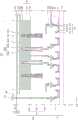
参考图1,非易失性存储器件10可以包括存储单元阵列20和外围电路30。存储单元阵列20包括多个存储单元块BLK1、BLK2、...、和BLKn。存储单元块BLK1、BLK2、...和BLKn可以各自包括多个存储单元。存储单元块BLK1、BLK2、...、和BLKn可以通过位线BL、字线WL、串选择线SSL和地选择线GSL连接到外围电路30。Referring to FIG. 1 , a
外围电路30可以包括行解码器32、页缓冲器34、数据输入/输出电路36和控制逻辑38。在一些实施例中,外围电路30还可以包括输入/输出接口、列逻辑、电压发生器、预解码器、温度传感器、命令解码器、地址解码器、放大器电路等。
存储单元阵列20可以通过位线BL连接到页缓冲器34,并且存储单元阵列20可以通过字线WL、串选择线SSL和地选择线GSL连接到行解码器32。在存储单元阵列20中,包括在存储单元块BLK1、BLK2、...、和BLKn中的每一个中的存储单元均可以是闪存单元。存储单元阵列20可以包括三维存储单元阵列。3D存储单元阵列可以包括多个NAND串,并且每个NAND串可以包括多个存储单元,该多个存储单元连接到竖直堆叠在衬底上的多条字线WL。The
外围电路30可以从非易失性存储器件10外部的器件接收地址ADDR、命令CMD和控制信号CTRL,并且可以向非易失性存储器件10外部的器件发送数据DATA和从非易失性存储器件10外部的器件接收数据DATA。The
行解码器32可以响应于并基于从外部接收的地址ADDR来选择存储单元块BLK1、BLK2、...、和BLKn中的至少一个,并且选择与所选择的存储单元块相对应的字线WL、串选择线SSL和地选择线GSL。行解码器32可以将用于执行存储操作的电压发送到与所选择的存储单元块相对应的字线WL。The
页缓冲器34可以通过位线BL连接到存储单元阵列20。页缓冲器34可以在编程操作期间作为写驱动器操作并且根据要存储在存储单元阵列20中的数据DATA向位线BL施加电压,并且可以在读取操作期间作为读出放大器操作并感测存储在存储单元阵列20中的数据DATA。页缓冲器34可以根据从控制逻辑38提供的控制信号CTRL操作。The
数据输入/输出电路36可以通过数据线DLs连接到页缓冲器34。在编程操作期间,数据输入/输出电路36可以从存储控制器接收数据DATA并且基于从控制逻辑38提供的列地址C_ADDR将要编程的数据DATA提供给页缓冲器34。数据输入/输出电路36可以在读取操作期间基于从控制逻辑38提供的列地址C_ADDR来将存储在页缓冲器34中要读取的数据DATA提供给存储控制器。The data input/
数据输入/输出电路36可以将输入到其中的地址或命令发送到控制逻辑38或行解码器32。在一些实施例中,外围电路30还包括静电放电(ESD)电路和上拉/下拉驱动器。Data input/
控制逻辑38可以从存储控制器接收命令CMD和控制信号CTRL。控制逻辑38可以将行地址R_ADDR提供给行解码器32并且将列地址C_ADDR提供给数据输入/输出电路36。控制逻辑38可以响应于控制信号CTRL而生成在非易失性存储器件10中使用的各种内部控制信号。例如,当执行诸如编程操作或擦除操作的存储操作时,控制逻辑38可以调整提供给字线WL和位线BL的电压电平。
图2是根据本发明构思的示例实施例的非易失性存储器件的示意性透视图。FIG. 2 is a schematic perspective view of a nonvolatile memory device according to example embodiments of the inventive concepts.
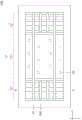
参考图2,非易失性存储器件10包括在竖直方向(例如,Z方向)上彼此重叠的单元阵列结构CS和外围电路结构PS。单元阵列结构CS可以包括上面参考图1描述的存储单元阵列20。外围电路结构PS可以包括上面参考图1描述的外围电路30。Referring to FIG. 2 , the
单元阵列结构CS可以包括存储单元块BLK1、BLK2、...、和BLKn。存储单元块BLK1、BLK2、...、和BLKn均可以包括三维布置的存储单元。The cell array structure CS may include memory cell blocks BLK1, BLK2, . . . , and BLKn. Each of the memory cell blocks BLK1, BLK2, . . . , and BLKn may include three-dimensionally arranged memory cells.
图3是根据本发明构思的示例实施例的非易失性存储器件的存储单元阵列的等效电路图。FIG. 3 is an equivalent circuit diagram of a memory cell array of a nonvolatile memory device according to example embodiments of the inventive concepts.
参考图3,存储单元阵列MCA可以包括多个存储单元串MS。存储单元阵列MCA可以包括多条位线BL:BL1、BL2、...、BLm、多条字线WL:WL1、WL2、...、WLn-1和WLn、至少一条串选择线SSL、至少一条地选择线GSL、以及公共源极线CSL。存储单元串MS可以形成在位线BL:BL1、BL2、...、BLm和公共源极线CSL之间。尽管图3示出了存储单元串MS均包括两条串选择线SSL的示例,但本发明构思不限于此。例如,存储单元串MS均可以包括一条串选择线SSL。Referring to FIG. 3, the memory cell array MCA may include a plurality of memory cell strings MS. The memory cell array MCA may include a plurality of bit lines BL: BL1, BL2, . . . , BLm, a plurality of word lines WL: WL1, WL2, . A ground selection line GSL, and a common source line CSL. A memory cell string MS may be formed between bit lines BL: BL1, BL2, . . . , BLm and a common source line CSL. Although FIG. 3 shows an example in which the memory cell strings MS each include two string selection lines SSL, the inventive concept is not limited thereto. For example, each of the memory cell strings MS may include a string selection line SSL.
存储单元串MS均可以包括串选择晶体管SST、地选择晶体管GST和多个存储单元晶体管MC1、MC2、...、MCn-1和MCn。串选择晶体管SST的漏极区可以连接到位线BL:BL1、BL2、...、和BLm,并且地选择晶体管GST的源极区可以连接到公共源极线CSL。公共源极线CSL可以是多个地选择晶体管GST的源极区共同连接的区域。Each of the memory cell strings MS may include a string selection transistor SST, a ground selection transistor GST, and a plurality of memory cell transistors MC1, MC2, . . . , MCn-1, and MCn. Drain regions of the string selection transistors SST may be connected to bit lines BL: BL1, BL2, . . . , and BLm, and source regions of the ground selection transistors GST may be connected to a common source line CSL. The common source line CSL may be a region where source regions of a plurality of ground selection transistors GST are commonly connected.
串选择晶体管SST可以连接到串选择线SSL,并且地选择晶体管GST可以连接到地选择线GSL。存储单元晶体管MC1、MC2、...、MCn-1和MCn可以分别连接到字线WL:WL1、WL2、...、WLn-1和WLn。The string selection transistor SST may be connected to a string selection line SSL, and the ground selection transistor GST may be connected to a ground selection line GSL. The memory cell transistors MC1, MC2, . . . , MCn-1, and MCn may be connected to word lines WL: WL1, WL2, . . . , WLn-1, and WLn, respectively.
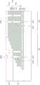
图4A是根据本发明构思的示例实施例的非易失性存储器件的截面图,并且图4B是图4A的区域A的放大图。FIG. 4A is a cross-sectional view of a nonvolatile memory device according to an example embodiment of the inventive concept, and FIG. 4B is an enlarged view of region A of FIG. 4A .
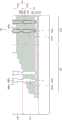
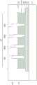
一起参考图4A和图4B,非易失性存储器件100包括第一结构S1和接合到第一结构S1的第二结构S2。第一结构S1可以接触第二结构S2,使得第一结构S1的多个第一接合焊盘BP1和第二结构S2的多个第二接合焊盘BP2分别彼此接触。在一些实施例中,当第一接合焊盘BP1包括铜(Cu)并且第二接合焊盘BP2包括Cu时,第一结构S1可以通过Cu-Cu接合来接合到第二结构S2。非易失性存储器件100还可以包括设置在第二结构S2上的连接层CL。Referring to FIGS. 4A and 4B together, the
第一结构S1可以包括第一衬底110、第一衬底110上的外围电路PC、第一衬底110和外围电路PC上的第一绝缘结构IL1、第一绝缘结构IL1上的第一接合焊盘BP1、以及第一绝缘结构IL1中的第一互连结构IC1。The first structure S1 may include a
第一衬底110可以包括半导体材料,例如IV族半导体材料、III-V族半导体材料和/或II-VI族半导体材料。IV族半导体材料可以包括例如硅(Si)、锗(Ge)或硅锗(SiGe)。III-V族半导体材料可以包括例如砷化镓(GaAs)、铟磷(InP)、镓磷(GaP)、铟砷(InAs)、铟锑(InSb)或砷化铟镓(InGaAs)。II-VI族半导体材料可以包括例如碲化锌(ZnTe)或硫化镉(CdS)。第一衬底110可以是体晶片或外延层。The
外围电路PC可以设置在第一衬底110上。外围电路PC可以包括多个晶体管120。在实施例中,晶体管120包括在第一衬底110上的栅电极122、在栅电极122和第一衬底110之间的栅极绝缘层121、在栅电极122的侧表面上的栅极间隔物123以及在栅电极122的两侧的源极/漏极124和125。A peripheral circuit PC may be disposed on the
第一绝缘结构IL1可以覆盖第一衬底110和外围电路PC。在一些实施例中,第一绝缘结构IL1可以包括堆叠在第一衬底110上的多个绝缘层。第一绝缘结构IL1可以包括绝缘材料,其包括例如氧化硅、氮化硅、低k材料或它们的组合。低k材料可以是介电常数低于氧化硅的介电常数的材料。例如,第一绝缘结构IL1可以包括磷硅玻璃(PSG)、硼磷硅玻璃(BPSG)、氟化硅酸盐玻璃(FSG)、有机硅酸盐玻璃(OSG)、旋涂玻璃(SOG)、旋涂聚合物、或其组合。在一些实施例中,第一绝缘结构IL1可以包括具有约2.2至约2.4的超低介电常数K的超低k(ULK)膜。ULK膜可以包括SiOC或SiCOH。The first insulating structure IL1 may cover the
第一接合焊盘BP1可以设置在第一绝缘结构IL1上。在一些实施例中,第一接合焊盘BP1的顶表面可以与第一绝缘结构IL1的顶表面共面。例如,在这些实施例中,第一接合焊盘BP1不从第一绝缘结构IL1的顶表面突出。第一接合焊盘BP1可以包括导电材料,该导电材料包括铜(Cu)、金(Au)、银(Ag)、铝(Al)、钨(W)、钛(Ti)、钽(Ta)或其组合。The first bonding pad BP1 may be disposed on the first insulating structure IL1. In some embodiments, the top surface of the first bonding pad BP1 may be coplanar with the top surface of the first insulating structure IL1. For example, in these embodiments, the first bonding pad BP1 does not protrude from the top surface of the first insulating structure IL1. The first bonding pad BP1 may include a conductive material including copper (Cu), gold (Au), silver (Ag), aluminum (Al), tungsten (W), titanium (Ti), tantalum (Ta), or its combination.
第一互连结构IC1可以设置在第一绝缘结构IL1中并且可以被第一绝缘结构IL1围绕。第一互连结构IC1可以连接到外围电路PC和第一接合焊盘BP1。第一互连结构IC1可以将外围电路PC连接到第一接合焊盘BP1和/或互连外围电路PC中的晶体管120。第一互连结构IC1可以包括多条线路、互连线路的通孔、以及互连线路和晶体管120的插塞。第一互连结构IC1可以包括诸如铜(Cu)、铝(Al)、钨(W)、银(Ag)、金(Au)或其组合的导电材料。The first interconnection structure IC1 may be disposed in the first insulating structure IL1 and may be surrounded by the first insulating structure IL1. The first interconnection structure IC1 may be connected to the peripheral circuit PC and the first bonding pad BP1. The first interconnect structure IC1 may connect the peripheral circuit PC to the first bonding pad BP1 and/or interconnect the
如本文所使用的,一个组件“在”或“设置在”另一组件“上”可以指的是两个组件在竖直方向(例如,Z方向)上彼此重叠。例如,设置在第二组件“上”的第一组件可以设置在第二组件上方或下方,并且可以直接接触第二组件或通过中间层与其分离。此外,如本文所使用的,“围绕”或“覆盖”可分别指至少部分地围绕或至少部分地覆盖。例如,如果层围绕组件,则该层可以围绕该组件的横向(例如水平)侧,并且该组件的其他侧可以被该层围绕或可以不被该层围绕,如将由参考的图和随附的上下文和描述所指示的。As used herein, one component "on" or "disposed on" another component may mean that two components overlap each other in a vertical direction (eg, Z direction). For example, a first component disposed "on" a second component may be disposed above or below the second component, and may directly contact the second component or be separated therefrom by an intervening layer. Also, as used herein, "surround" or "cover" may mean at least partially surrounding or at least partially covering, respectively. For example, if a layer surrounds a component, the layer may surround one lateral (e.g., horizontal) side of the component, and the other sides of the component may or may not be surrounded by the layer, as will be described in the referenced figures and accompanying as the context and description dictate.
第二结构S2可以包括导电蚀刻停止层270、在导电蚀刻停止层270上的公共源极线层210、在公共源极线层210上的堆叠结构SS、穿透堆叠结构SS的单元区域CELL的多个沟道结构240、穿透堆叠结构SS的阶梯区域EXT的多个虚设沟道结构280、在堆叠结构SS上(例如,接触堆叠结构SS)的第二绝缘结构IL2、在第二绝缘结构IL2上的第二接合焊盘BP2、以及设置在第二绝缘结构IL2中并被第二绝缘结构IL2围绕的第二互连结构IC2。第二结构S2可以设置在第一结构S1上,使得第二绝缘结构IL2接触第一绝缘结构IL1并且第二接合焊盘BP2分别对应于第一接合焊盘BP1。The second structure S2 may include a conductive
在一些实施例中,第二结构S2还可以包括设置在公共源极线层210和堆叠结构SS之间的下导电层250。在一些实施例中,第二结构S2还可以包括设置在下导电层250和堆叠结构SS之间的下支撑层260。In some embodiments, the second structure S2 may further include a lower
公共源极线层210可以包括半导体材料,例如IV族半导体材料、III-V族半导体材料和II-VI族半导体材料。在一些实施例中,公共源极线层210可以包括不包含碳的半导体材料。公共源极线层210可以包括例如多晶硅。在一些实施例中,公共源极线层210可以包括不包含碳的多晶硅。导电蚀刻停止层270可以接触公共源极线层210并且用作公共源极线的一部分。导电蚀刻停止层270可以包括电阻率小于构成公共源极线层210的材料的电阻率的材料。在一些实施例中,导电蚀刻停止层270可以包括包含碳的导电材料。例如,导电蚀刻停止层270可以包括包含约1原子%(也被称为原子百分比)或更多碳的多晶硅。例如,导电蚀刻停止层270可以包括包含约1原子%至约5原子%碳的多晶硅。在一些其他实施例中,导电蚀刻停止层270可以包括低电阻导电材料,例如金属或导电金属氮化物。例如,导电蚀刻停止层270可以包括Cu、Al、W、Ag、Au或TiN。导电蚀刻停止层270可以具有从约

堆叠结构SS可以设置在公共源极线层210上。堆叠结构SS可以包括交替堆叠在公共源极线层210上的多个栅极层230a和230b以及多个层间绝缘层220a和220b。例如,每个栅极层可以与层间绝缘层交替堆叠。堆叠结构SS可以包括在公共源极线层210上的第一部分SSa和在第一部分SSa上的第二部分SSb。堆叠结构SS的第一部分SSa可以包括交替堆叠在公共源极线层210上的多个第一栅极层230a和多个第一层间绝缘层220a。堆叠结构SS的第二部分SSb可以包括交替堆叠在堆叠结构SS的第一部分SSa上的多个第二栅极层230b和多个第二层间绝缘层220b。The stack structure SS may be disposed on the common
堆叠结构SS可以包括单元区域CELL和阶梯区域EXT。堆叠结构SS的阶梯区域EXT可以位于堆叠结构SS的单元区域CELL的一侧并且可以具有阶梯形状。例如,堆叠结构SS的阶梯区域EXT可以具有沿+Z方向下降的阶梯形状。The stack structure SS may include a cell area CELL and a step area EXT. The stair region EXT of the stack structure SS may be located at one side of the cell region CELL of the stack structure SS and may have a stair shape. For example, the stair region EXT of the stack structure SS may have a stair shape descending in the +Z direction.
栅极层230a和230b可以包括但不限于导电材料,导电材料包括钨(W)、铜(Cu)、银(Ag)、金(Au)、铝(Al)或其组合。层间绝缘层220a和220b可以包括绝缘材料,该绝缘材料可以包括氧化硅、氮化硅、低k材料或其组合。The gate layers 230a and 230b may include, but are not limited to, conductive materials including tungsten (W), copper (Cu), silver (Ag), gold (Au), aluminum (Al), or combinations thereof. The insulating
沟道结构240均可以穿透堆叠结构SS的单元区域CELL并且接触公共源极线层210。在一些实施例中,沟道结构240均可以穿透堆叠结构SS的单元区域CELL、下导电层250和下支撑层260并且接触公共源极线层210。Each of the
参考图4B,沟道结构240可以形成在第一沟道孔240Ha和第二沟道孔240Hb中。沟道结构240可以包括设置在第一沟道孔240Ha和第二沟道孔240Hb的内壁上的栅极绝缘层241以及在栅极绝缘层241上或邻近栅极绝缘层241的沟道层242。在一些实施例中,沟道结构240可以包括在沟道层242上或邻近沟道层242的掩埋绝缘层243、以及位于第二沟道孔240Hb的端部处的沟道焊盘244。Referring to FIG. 4B , a
栅极绝缘层241可以在公共源极线层210和沟道层242之间以及在堆叠结构SS和沟道层242之间延伸。栅极绝缘层241可以包括顺序堆叠在第一沟道孔240Ha和第二沟道孔240Hb的内壁上的阻挡绝缘层241a、电荷存储层241b和隧穿绝缘层241c。阻挡绝缘层241a可以包括例如氧化硅、氮化硅、介电常数大于氧化硅的介电常数的金属氧化物或其组合。金属氧化物可包括例如氧化铪、氧化铝、氧化锆、氧化钽或其组合。电荷存储层241b可以包括例如氮化硅、氮化硼、多晶硅或其组合。隧穿绝缘层241c可以包括例如金属氧化物或氧化硅。在一些实施例中,阻挡绝缘层241a、电荷存储层241b和隧穿绝缘层241c可以分别包括氧化物、氮化物和氧化物。The
沟道层242可以围绕掩埋绝缘层243的侧表面和一端。例如,沟道层242可以围绕掩埋绝缘层243的远离沟道焊盘244的端部。沟道层242可以包括半导体材料,例如IV族半导体材料、III-V族半导体材料和II-VI族半导体材料。在一些实施例中,沟道层242可以包括多晶硅。The
掩埋绝缘层243可以填充由沟道层242和沟道焊盘244限定的空间。掩埋绝缘层243可以包括绝缘材料,该绝缘材料可以包括例如氮化硅、氧化硅、低k材料或其组合。在一些实施例中,掩埋绝缘层243可以包括氧化硅。The buried insulating
沟道焊盘244可以接触沟道层242和掩埋绝缘层243。在一些实施例中,沟道焊盘244也可以接触栅极绝缘层241。沟道焊盘244可以包括:半导体材料,例如硅(Si)、锗(Ge)或硅锗(Si-Ge);金属,例如钨(W)、钛(Ti)、铝(Al)、铜(Cu)、金(Au)和银(Ag);金属氮化物,例如氮化钛(TiN)或氮化钽(TaN);或导电材料,例如其组合。在一些实施例中,沟道焊盘244可以包括多晶硅。The
返回参考图4A,虚设沟道结构280可以穿透堆叠结构SS的阶梯区域EXT并接触公共源极线层210。在一些实施例中,虚设沟道结构280可以穿透堆叠结构SS的阶梯区域EXT、下导电层250和下支撑层260并且接触公共源极线层210。虚设沟道结构280还可以穿透第二绝缘结构IL2的第二部分IL2b和第三部分IL2c。虚设沟道结构280可以形成在穿透堆叠结构SS的阶梯区域EXT和第二绝缘结构IL2的第三部分IL2c的第一虚设沟道孔280Ha中,以及形成在穿透第二绝缘结构IL2的第二部分IL2b的第二虚设沟道孔280Hb中。Referring back to FIG. 4A , the
虚设沟道结构280可以包括在第一虚设沟道孔280Ha和第二虚设沟道孔280Hb上的绝缘层282以及在绝缘层282上的导电层281。导电层281可以在第一虚设沟道孔280Ha和第二虚设沟道孔280Hb中延伸并且接触公共源极线层210。绝缘层282可以在导电层281和堆叠结构SS的阶梯区域EXT之间延伸。绝缘层282还可以在导电层281和第二绝缘结构IL2的第二部分IL2b之间延伸。绝缘层282还可以在导电层281和第二绝缘结构IL2的第三部分IL2c之间延伸。在一些实施例中,绝缘层282还可以在导电层281和下支撑层260之间延伸。在一些实施例中,绝缘层282还可以在导电层281和下导电层250之间延伸。在一些实施例中,绝缘层282的厚度可以大于栅极绝缘层241的厚度。The
导电层281可以包括半导体材料或诸如金属的导电材料。导电层281可以包括例如多晶硅、铜(Cu)、钨(W)、铝(Al)、金(Au)、银(Ag)或其组合。绝缘层282可以包括例如氧化硅、氮化硅、低k材料或其组合。The
穿透堆叠结构SS的阶梯区域EXT的虚设沟道结构280可以用作公共源极线接触并且接触公共源极线层210。由于不需要在堆叠结构SS外部由接触公共源极线层210的公共源极线接触占据的平面区域,因此可以减小非易失性存储器件100的平面区域。The
第二绝缘结构IL2可以覆盖堆叠结构SS、沟道结构240和虚设沟道结构280。第二绝缘结构IL2可以包括多个绝缘层。例如,第二绝缘结构IL2可以包括第一部分IL2a、在第一部分IL2a上的第二部分IL2b以及在第二部分IL2b上的第三部分IL2c。第二绝缘结构IL2可以包括例如绝缘材料,该绝缘材料可以包括氧化硅、氮化硅、低k材料或其组合。The second insulation structure IL2 may cover the stack structure SS, the
第二接合焊盘BP2可以布置在第二绝缘结构IL2上。在一些实施例中,第二接合焊盘BP2的顶表面可以与第二绝缘结构IL2的底表面共面。例如,在实施例中,第二接合焊盘BP2不从第二绝缘结构IL2的底表面突出。第二接合焊盘BP2可以包括导电材料,该导电材料可以包括铜(Cu)、金(Au)、银(Ag)、铝(Al)、钨(W)、钛(Ti)、钽(Ta)或其组合。The second bonding pad BP2 may be disposed on the second insulating structure IL2. In some embodiments, a top surface of the second bonding pad BP2 may be coplanar with a bottom surface of the second insulating structure IL2. For example, in an embodiment, the second bonding pad BP2 does not protrude from the bottom surface of the second insulating structure IL2. The second bonding pad BP2 may include a conductive material, and the conductive material may include copper (Cu), gold (Au), silver (Ag), aluminum (Al), tungsten (W), titanium (Ti), tantalum (Ta) or a combination thereof.
第二互连结构IC2可以设置在第二绝缘结构IL2中并且可以被第二绝缘结构IL2围绕。第二互连结构IC2可以连接到栅极层230a和230b、沟道结构240、虚设沟道结构280和第二接合焊盘BP2。例如,第二互连结构IC2可以将栅极层230a和230b、沟道结构240和虚设沟道结构280连接到第二接合焊盘BP2。The second interconnection structure IC2 may be disposed in the second insulating structure IL2 and may be surrounded by the second insulating structure IL2. The second interconnection structure IC2 may be connected to the
栅极层230a和230b可以通过第二互连结构IC2、第二接合焊盘BP2、第一接合焊盘BP1和第一互连结构IC1连接到外围电路PC。沟道结构240可以通过第二互连结构IC2、第二接合焊盘BP2、第一接合焊盘BP1和第一互连结构IC1连接到外围电路PC。虚设沟道结构280可以通过第二互连结构IC2、第二接合焊盘BP2、第一接合焊盘BP1和第一互连结构IC1连接到外围电路PC。输入/输出焊盘294可以通过第二互连结构IC2、第二接合焊盘BP2、第一接合焊盘BP1和第一互连结构IC1连接到外围电路PC。The gate layers 230a and 230b may be connected to the peripheral circuit PC through the second interconnection structure IC2, the second bonding pad BP2, the first bonding pad BP1, and the first interconnection structure IC1. The
第二互连结构IC2可以包括多条线路、互连线路的通孔、以及接触栅极层230a和230b、沟道结构240、虚设沟道结构280和输入/输出焊盘294的多个插塞。第二互连结构IC2可以包括诸如铜(Cu)、铝(Al)、钨(W)、银(Ag)、金(Au)或其组合的导电材料。The second interconnection structure IC2 may include a plurality of lines, vias for interconnecting the lines, and a plurality of plugs contacting the
下导电层250可以在下支撑层260和公共源极线层210之间延伸。下导电层250可以包括半导体材料或诸如金属的导电材料。下导电层250可以包括多晶硅、铝(Al)、钨(W)、银(Ag)、金(Au)或其组合。在一些实施例中,如图4B所示,下导电层250可以穿透栅极绝缘层241并接触沟道层242。The lower
下支撑层260可以在堆叠结构SS和下导电层250之间延伸。下支撑层260可以包括半导体材料或诸如金属的导电材料。下支撑层260可以包括多晶硅、铝(Al)、钨(W)、银(Ag)、金(Au)或其组合。在一些实施例中,当公共源极线层210、下导电层250和下支撑层260中的每一个包括多晶硅时,公共源极线层210和下导电层250之间的边界以及下导电层250和下支撑层260之间的边界可能不清楚或无法识别。The
连接层CL可以设置在第二结构S2上。连接层CL可以包括覆盖第二绝缘结构IL2和导电蚀刻停止层270的第三绝缘结构IL3、穿透第三绝缘结构IL3的输入/输出通孔292、设置在绝缘结构IL3上的输入/输出焊盘294、覆盖第三绝缘结构IL3和输入/输出焊盘294的第四绝缘结构IL4、以及穿透第四绝缘结构IL4并连接到输入/输出焊盘294的外部连接焊盘296。A connection layer CL may be provided on the second structure S2. The connection layer CL may include a third insulating structure IL3 covering the second insulating structure IL2 and the conductive
第三绝缘结构IL3可以设置在第二绝缘结构IL2和导电蚀刻停止层270上。在一些实施例中,第三绝缘结构IL3可以包括多个堆叠的绝缘层。第三绝缘结构IL3可以包括例如绝缘材料,如氧化硅、氮化硅、低k材料或其组合。在一些实施例中,第三绝缘结构IL3可以包括原硅酸四乙酯(TEOS)。The third insulating structure IL3 may be disposed on the second insulating structure IL2 and the conductive
导电蚀刻停止层270的顶表面(例如导电蚀刻停止层270和第三绝缘结构IL3之间的界面)可以位于第一竖直高度LV1处。第二绝缘结构IL2的顶表面(例如,第二绝缘结构IL2和第三绝缘结构IL3之间的界面)可以位于第二竖直高度LV2处。导电蚀刻停止层270的底表面(例如导电蚀刻停止层270和公共源极线层210之间的界面)可以位于第三竖直高度LV3处。第一竖直高度LV1可以高于第二竖直高度LV2和第三竖直高度LV3(例如,在+Z方向上),并且第二竖直高度LV2可以高于第三竖直高度LV3。然而,第二竖直高度LV2可以低于第一竖直高度LV1,因此第二竖直高度LV2可以位于第一竖直高度LV1和第三竖直高度LV3之间。A top surface of the conductive etch stop layer 270 (eg, an interface between the conductive
例如,第二绝缘结构IL2的顶表面可以位于比导电蚀刻停止层270的顶表面的竖直高度低的竖直高度处,并且第三绝缘结构IL3的底表面中与第二绝缘结构IL2的顶表面接触的一部分可以位于比第三绝缘结构IL3的底表面中与导电蚀刻停止层270的顶表面接触的一部分的竖直高度低的竖直高度处。因此,导电蚀刻停止层270的侧表面的上部可以被第三绝缘结构IL3覆盖,并且导电蚀刻停止层270的侧表面的下部可以被第二绝缘结构IL2覆盖。For example, the top surface of the second insulating structure IL2 may be located at a vertical height lower than that of the top surface of the conductive
如图7M所示,在去除图7L所示的第二衬底215的工艺期间,导电蚀刻停止层270可以用作蚀刻停止层。为了如图7M所示完全去除图7L中的第二衬底215,甚至在暴露第二绝缘结构IL2之后,也可以执行过蚀刻,并且由于导电蚀刻停止层270和第二绝缘结构IL2之间的蚀刻选择性差异,图7L所示的第二绝缘结构IL2的上部可以被部分去除,因此第二绝缘结构IL2的顶表面可以变得低于导电蚀刻停止层270的顶表面。在一些实施例中,第二竖直高度LV2可以比第一竖直高度LV1低约

输入/输出通孔292可以穿透第三绝缘结构IL3并且可以连接到第二互连结构IC2,并且输入/输出焊盘294可以设置在第三绝缘结构IL3上并且可以连接到输入/输出通孔292。输入/输出焊盘294可以通过输入/输出通孔292和第二互连结构IC2连接到第二接合焊盘BP2。The input/output via
输入/输出通孔292和输入/输出焊盘294可以包括导电材料,例如铜(Cu)、铝(Al)、钨(W)、银(Ag)或金(Au)。The input/
围绕输入/输出焊盘294的第四绝缘结构IL4可以设置在第三绝缘结构IL3上。第四绝缘结构IL4可以覆盖第三绝缘结构IL3的顶表面和输入/输出焊盘294的侧表面,而第四绝缘结构IL4可能不覆盖并暴露输入/输出焊盘294的顶表面的至少一部分。例如,第四绝缘结构IL4可以包括可光成像电介质(PID)材料或光敏聚酰亚胺(PSPI)。外部连接焊盘296可以穿透第四绝缘结构IL4并且可以连接到输入/输出焊盘294。在一些实施例中,外部连接焊盘296可以从第四绝缘结构IL4的顶表面向上突出。外部连接焊盘296和输入/输出焊盘294可以包括导电材料,例如铜(Cu)、铝(Al)、钨(W)、银(Ag)或金(Au)。外部连接焊盘296可以暴露于非易失性存储器件100的外部。外部连接焊盘296可以连接到在非易失性存储器件100外部的存储控制器,如稍后将参考图9和图10所描述的。A fourth insulating structure IL4 surrounding the input/
图5A是根据本发明构思的示例实施例的非易失性存储器件的底视图,并且图5B是沿图5A的线B-B′截取的截面图。5A is a bottom view of a nonvolatile memory device according to an example embodiment of the inventive concept, and FIG. 5B is a cross-sectional view taken along line B-B' of FIG. 5A.
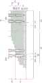
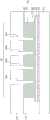
一起参考图5A和图5B,非易失性存储器件100A的与以上参考图4A和图4B所描述的非易失性存储器件100类似的实施例可以包括第一结构S1和接合到第一结构S1的第二结构S2A。非易失性存储器件100A还可以包括设置在第二结构S2A上的连接层CL。由于第一结构S1和连接层CL与上面参考图4A描述的第一结构S1和连接层CL基本相同,可以省略与上面已经给出的描述相同的描述。Referring to FIGS. 5A and 5B together, an embodiment of a
第二结构S2A还可以包括字线切口结构WS和虚设字线切口结构DWS。在一些实施例中,第二结构S2A可以包括图4A所示的虚没沟道结构280或具有与沟道结构240基本相同的配置的虚设沟道结构。The second structure S2A may further include a word line slit structure WS and a dummy word line slit structure DWS. In some embodiments, the second structure S2A may include the
字线切口结构WS可以穿透堆叠结构SS并且可以沿第一水平方向(例如,X方向)延伸。字线切口结构WS可以在竖直方向(例如,Z方向)上穿透堆叠结构SS的阶梯区域EXT和单元区域CELL。字线切口结构WS还可以穿透第二绝缘结构IL2的第二部分IL2b和下支撑层260。字线切口结构WS可以形成在穿透堆叠结构SS的字线切口WSH中。字线切口WSH还可以穿透第二绝缘结构IL2的第二部分IL2b和下支撑层260。字线切口结构WS可以包括例如包括氧化硅、氮化硅、低k材料或其组合的绝缘材料。The word line slit structure WS may penetrate the stack structure SS and may extend along a first horizontal direction (eg, X direction). The word line slit structure WS may penetrate the step region EXT and the cell region CELL of the stack structure SS in a vertical direction (eg, Z direction). The word line slit structure WS may also penetrate the second portion IL2b of the second insulation structure IL2 and the
虚设字线切口结构DWS可以在竖直方向(例如,Z方向)上穿透堆叠结构SS的阶梯区域EXT,并且可以沿第一水平方向(例如,X方向)延伸。虚设字线切口结构DWS可以位于堆叠结构SS的阶梯区域EXT中并且可以不穿透堆叠结构SS的单元区域CELL。虚设字线切口结构DWS还可以穿透第二绝缘结构IL2的第二部分IL2b和下支撑层260。虚设字线切口结构DWS可以形成在穿透堆叠结构SS的阶梯区域EXT的虚设字线切口DWSH中。虚设字线切口DWSH还可以穿透第二绝缘结构IL2的第二部分IL2b和下支撑层260。The dummy word line slit structure DWS may penetrate the stair region EXT of the stack structure SS in a vertical direction (eg, Z direction), and may extend in a first horizontal direction (eg, X direction). The dummy word line slit structure DWS may be located in the step region EXT of the stack structure SS and may not penetrate the cell region CELL of the stack structure SS. The dummy word line slit structure DWS may also penetrate the second portion IL2b of the second insulation structure IL2 and the
在一些实施例中,虚设字线切口结构DWS不直接接触公共源极线层210并且可以通过下导电层250与公共源极线层210电接触。在另一实施例中,虚设字线切口结构DWS可以穿透下导电层250并直接接触公共源极线层210。In some embodiments, the dummy word line slit structure DWS does not directly contact the common
虚设字线切口结构DWS可以包括与公共源极线层210接触的导电层DWSa和在导电层DWSa和堆叠结构SS之间的绝缘层DWSb。在一些实施例中,导电层DWSa不直接接触公共源极线层210并且可以通过下导电层250与公共源极线层210电接触。绝缘层DWSb还可以在导电层DWSa和第二绝缘结构IL2的第二部分IL2b之间延伸。在一些实施例中,绝缘层DWSb还可以在导电层DWSa和下支撑层260之间延伸。例如,绝缘层DWSb可以设置在虚设字线切口DWSH上。The dummy word line slit structure DWS may include a conductive layer DWSa in contact with the common
导电层DWSa可以包括例如多晶硅、铜(Cu)、钨(W)、铝(Al)、金(Au)、银(Ag)或其组合。绝缘层DWSb可以包括例如氧化硅、氮化硅、低k材料或其组合。The conductive layer DWSa may include, for example, polysilicon, copper (Cu), tungsten (W), aluminum (Al), gold (Au), silver (Ag), or combinations thereof. The insulating layer DWSb may include, for example, silicon oxide, silicon nitride, a low-k material, or a combination thereof.
第二互连结构IC2还可以连接到虚设字线切口结构DWS。例如,虚设字线切口结构DWS可以通过第二互连结构IC2、第二接合焊盘BP2、第一接合焊盘BP1和第一互连结构IC1连接到外围电路PC。然而,即使当第二互连结构IC2连接到虚设字线切口结构DWS时,第二互连结构IC2也可能不连接到字线切口结构WS。The second interconnect structure IC2 may also be connected to the dummy word line slit structure DWS. For example, the dummy word line slit structure DWS may be connected to the peripheral circuit PC through the second interconnection structure IC2 , the second bonding pad BP2 , the first bonding pad BP1 and the first interconnection structure IC1 . However, even when the second interconnect structure IC2 is connected to the dummy word line slit structure DWS, the second interconnect structure IC2 may not be connected to the word line slit structure WS.
在根据本发明构思的非易失性存储器件100A中,由于穿透堆叠结构SS的阶梯区域EXT的虚设字线切口结构DWS被用作用于公共源极线层210的公共源极线接触,因此可以不包括单独的公共源极线接触,并且因此非易失性存储器件100A可以具有减小的平面区域。此外,通过去除对单独的公共源极线接触的需要,可以减少根据本发明构思的非易失性存储器件的制造步骤的数量以及制造成本。In the
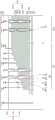
图6和图7A至图7N是用于描述根据本发明构思的示例实施例的制造非易失性存储器件的方法的截面图。6 and 7A to 7N are cross-sectional views for describing a method of manufacturing a nonvolatile memory device according to example embodiments of the inventive concepts.
参考图6,晶体管120可以形成在第一衬底110上,并且覆盖晶体管120的第一绝缘结构IL1和被第一绝缘结构IL1围绕的第一互连结构IC1可以形成在第一衬底110上,从而形成外围电路PC。晶体管120均可以形成为包括在第一衬底110上的栅电极122、在栅电极122和第一衬底110之间的栅极绝缘层121、在栅电极122的侧表面上的栅极间隔物123、以及在栅电极122的两侧的源极/漏极124和125。第一接合焊盘BP1可以形成在第一绝缘结构IL1上,从而完成第一结构S1。Referring to FIG. 6 , a
参考图7A,制备第二衬底215。第二衬底215可以包括半导体材料,例如IV族半导体材料、III-V族半导体材料和II-VI族半导体材料。公共源极线层210可以形成在第二衬底215上。初步堆叠结构的第一部分PSa可以形成在公共源极线层210上。可以通过在公共源极线层210上交替地形成第一层间绝缘层220a和多个第一牺牲层235a来形成初步堆叠结构的第一部分PSa。第一牺牲层235a均可以包括相对于第一层间绝缘层220a中的每一个具有蚀刻选择性的材料。例如,当第一层间绝缘层220a包括氧化硅时,第一牺牲层235a可以包括氮化硅。通过图案化初步堆叠结构的第一部分PSa,初步堆叠结构的第一部分PSa的阶梯区域EXT可以形成为阶梯形状。Referring to FIG. 7A, a
导电蚀刻停止层270可以形成在第二衬底215和公共源极线层210之间。公共源极线层210和导电蚀刻停止层270可以在竖直方向上彼此重叠并且具有基本相同的水平宽度和相同的水平区域。A conductive
在一些实施例中,下牺牲层255可以形成在公共源极线层210和初步堆叠结构的第一部分PSa之间。在一些实施例中,下支撑层260还可以形成在下牺牲层255和初步堆叠结构的第一部分PSa之间;例如,下支撑层260可以形成在下牺牲层255上。下牺牲层255可以包括相对于公共源极线层210和下支撑层260具有蚀刻选择性的材料。例如,当公共源极线层210和下支撑层260包括多晶硅时,下牺牲层255可以包括氮化硅。In some embodiments, the lower
第二绝缘结构的第三部分IL2c可以形成在第二衬底215和初步堆叠结构的第一部分PSa上,并且可以形成穿透初步堆叠结构的第一部分PSa的单元区域CELL和初步堆叠结构的第一部分PSa的阶梯区域EXT的第一虚设沟道孔280Ha。第一虚设沟道孔280Ha还可以穿透第二绝缘结构的第三部分IL2c。第一沟道孔240Ha和第一虚设沟道孔280Ha还可以穿透下支撑层260和下牺牲层255。The third part IL2c of the second insulating structure may be formed on the
第一沟道孔240Ha和第一虚设沟道孔280Ha可以分别填充有第一填充层240Fa和第一虚设填充层280Fa。在一些实施例中,第一填充层240Fa和第一虚设填充层280Fa可以包括多晶硅。The first channel hole 240Ha and the first dummy channel hole 280Ha may be filled with the first filling layer 240Fa and the first dummy filling layer 280Fa, respectively. In some embodiments, the first filling layer 240Fa and the first dummy filling layer 280Fa may include polysilicon.
参考图7B,初步堆叠结构PS的第二部分PSb可以形成在初步堆叠结构PS的第一部分PSa上。初步堆叠结构PS可以包括第一部分PSa和第二部分PSb。可以通过在初步堆叠结构PS的第一部分PSa上交替地形成第二层间绝缘层220b和多个第二牺牲层235b来形成初步堆叠结构PS的第二部分PSb。第二牺牲层235b均可以包括相对于第二层间绝缘层220b中的每一个具有蚀刻选择性的材料。例如,当第二层间绝缘层220b包括氧化硅时,第二牺牲层235b可以包括氮化硅。通过图案化初步堆叠结构PS的第二部分PSb,初步堆叠结构PS的第二部分PSb的阶梯区域EXT可以形成为阶梯形状。Referring to FIG. 7B , the second part PSb of the preliminary stack structure PS may be formed on the first part PSa of the preliminary stack structure PS. The preliminary stack structure PS may include a first part PSa and a second part PSb. The second part PSb of the preliminary stack structure PS may be formed by alternately forming the second
第二绝缘结构的第二部分IL2b可以形成在第二绝缘结构的第三部分IL2c以及初步堆叠结构PS的第一部分PSa和第二部分PSb上。此后,可以形成穿透初步堆叠结构PS的第二部分PSb并暴露第一填充层240Fa的第二沟道孔240Hb和穿透第二绝缘结构的第二部分IL2b并暴露第一虚设填充层280Fa的第二虚设沟道孔280Hb。The second portion IL2b of the second insulating structure may be formed on the third portion IL2c of the second insulating structure and the first and second portions PSa and PSb of the preliminary stack structure PS. Thereafter, the second channel hole 240Hb penetrating the second portion PSb of the preliminary stack structure PS and exposing the first filling layer 240Fa and the second portion IL2b penetrating the second insulating structure and exposing the first dummy filling layer 280Fa may be formed. The second dummy channel hole 280Hb.
参考图7C,第二填充层240Fb和第二虚设填充层280Fb可以分别填充第二沟道孔240Hb和第二虚设沟道孔280Hb。在一些实施例中,第二填充层240Fb和第二虚设填充层280Fb可以包括多晶硅。Referring to FIG. 7C , the second filling layer 240Fb and the second dummy filling layer 280Fb may fill the second channel hole 240Hb and the second dummy channel hole 280Hb, respectively. In some embodiments, the second filling layer 240Fb and the second dummy filling layer 280Fb may include polysilicon.
一起参考图7C和图7D,可以从第一沟道孔240Ha和第二沟道孔240Hb去除第一填充层240Fa和第二填充层240Fb。为了防止第一虚设填充层280Fa和第二虚设填充层280Fb在去除第一填充层240Fa和第二填充层240Fb期间被去除,可以在去除第一填充层240Fa和第二填充层240Fb之前形成覆盖第二虚设填充层280Fb并暴露第二填充层240Fb的掩模。在去除第一填充层240Fa和第二填充层240Fb之后,可以去除掩模。沟道结构240可以形成在去除了第一填充层240Fa和第二填充层240Fb的第一沟道孔240Ha和第二沟道孔240Hb中。Referring to FIGS. 7C and 7D together, the first and second filling layers 240Fa and 240Fb may be removed from the first and second channel holes 240Ha and 240Hb. In order to prevent the first dummy filling layer 280Fa and the second dummy filling layer 280Fb from being removed during the removal of the first filling layer 240Fa and the second filling layer 240Fb, a covering first filling layer 240Fa and the second filling layer 240Fb may be formed before removing the first filling layer 240Fa and the second filling layer 240Fb. A mask for dummy filling layer 280Fb and exposing second filling layer 240Fb. After removing the first filling layer 240Fa and the second filling layer 240Fb, the mask may be removed. The
一起参考图7D和图4B,可以形成覆盖第一沟道孔240Ha和第二沟道孔240Hb的内壁的栅极绝缘层241。例如,阻挡绝缘层241a、电荷存储层241b和隧穿绝缘层241c可以顺序地形成在第一沟道孔240Ha和第二沟道孔240Hb的内壁上,从而形成栅极绝缘层241。沟道层242可以形成在栅极绝缘层241上,并且掩埋绝缘层243可以形成在沟道层242上。掩埋绝缘层243可以与栅极绝缘层241和沟道层242一起填充第一沟道孔240Ha和第二沟道孔240Hb。Referring to FIGS. 7D and 4B together, a
此后,可以去除栅极绝缘层241、沟道层242和掩埋绝缘层243的填充第二沟道孔240Hb的上端部分的部分,并且可以形成填充第二沟道孔240Hb的上端部分的沟道焊盘244,从而形成包括栅极绝缘层241、沟道层242、掩埋绝缘层243和沟道焊盘244的沟道结构240。Thereafter, portions of the
一起参考图7D、图7E和图4B,可以从第一虚设沟道孔280Ha和第二虚没沟道孔280Hb去除第一虚设填充层280Fa和第二虚设填充层280Fb。在一些实施例中,为了防止沟道结构240在去除第一虚设填充层280Fa和第二虚设填充层280Fb期间被去除,可以在去除第一虚设填充层280Fa和第二虚设填充层280Fb之前形成覆盖沟道结构240并暴露第二虚设填充层280Fb的掩模。在去除第一虚设填充层280Fa和第二虚设填充层280Fb之后,可以去除掩模。Referring to FIGS. 7D , 7E and 4B together, the first dummy filling layer 280Fa and the second dummy filling layer 280Fb may be removed from the first dummy channel hole 280Ha and the second dummy channel hole 280Hb. In some embodiments, in order to prevent the
接下来,虚设沟道结构280可以形成在第一虚设沟道孔280Ha和第二虚设沟道孔280Hb中。首先,绝缘层282可以形成在第一虚设沟道孔280Ha和第二虚设沟道孔280Hb的内壁上。例如,绝缘层282可以形成在第二绝缘结构的第二部分IL2b的顶表面上、第二虚设沟道孔280Hb的内壁上以及第一虚设沟道孔280Ha的内壁和底表面上。可以对绝缘层282进行各向异性蚀刻,从而去除绝缘层282在第二绝缘结构的第二部分IL2b的顶表面和第一虚设沟道孔280Ha的底表面上的部分。在一些实施例中,绝缘层282可以形成为比栅极绝缘层241厚。接下来,可以在绝缘层282上形成导电层281,因此可以形成包括导电层281和绝缘层282的虚设沟道结构280。导电层281可以与绝缘层282一起填充第一虚设沟道孔280Ha和第二虚设沟道孔280Hb。Next, a
一起参考图7E、图7F和图4B,可以通过去除下牺牲层255来在公共源极线层210和下支撑层260之间形成空间255H。沟道结构240的栅极绝缘层241和虚设沟道结构280的绝缘层282可以暴露在空间255H中。在去除下牺牲层255之前,可以形成穿透初步堆叠结构PS的第一部分PSa和第二部分PSb以及下支撑层260并暴露下牺牲层255的字线切口WSH。蚀刻剂可以通过字线切口WSH到达下牺牲层255并蚀刻下牺牲层255。Referring to FIGS. 7E , 7F and 4B together, a
一起参考图7F、图7G和图4B,可以去除沟道结构240的栅极绝缘层241的暴露在空间255H中的一部分以形成穿透栅极绝缘层241的开口240P。沟道层242可以通过开口240P暴露在空间255H中。在一些实施例中,虚设沟道结构280的绝缘层282可以具有足以在去除沟道结构240的栅极绝缘层241的一部分期间不被完全去除的厚度,因此导电层281可以不暴露在空间255H中。在另一实施例中,虚设沟道结构280的绝缘层282可以暴露于用于去除沟道结构240的栅极绝缘层241的一部分的蚀刻剂,并且可以蚀刻绝缘层282的暴露部分,从而在空间255H中暴露导电层281。Referring to FIGS. 7F , 7G and 4B together, a portion of the
一起参考图7G、图7H和图4B,可以通过填充空间255H来形成下导电层250。下导电层250可以通过开口240P接触沟道层242。在一些实施例中,下导电层250可以不与导电层281接触。在一些其他实施例中,与图7H所示不同,下导电层250可以穿透绝缘层282并接触导电层281。Referring to FIGS. 7G , 7H and 4B together, the lower
参考图7H和图7I,可以去除第一牺牲层235a和第二牺牲层235b以在第一层间绝缘层220a和第二层间绝缘层220b之间形成多个空间235Ha和235Hb。7H and 7I, the first
一起参考图7I和图7J,栅极层230a和230b可以形成为分别填充层间绝缘层220a和220b之间的空间235Ha和235Hb。以这种方式,可以形成包括第一部分SSa和第二部分SSb的堆叠结构SS,第一部分SSa包括交替堆叠在公共源极线层210上的第一层间绝缘层220a和第一栅极层230a,第二部分SSb包括交替堆叠在第一部分SSa上的第二层间绝缘层220b和第二栅极层230b。Referring to FIGS. 7I and 7J together,
参考图7K,第二绝缘结构IL2的第一部分IL2a可以形成在第二绝缘结构IL2的第二部分IL2b和堆叠结构SS上,从而完成包括第一部分IL2a、第二部分IL2b和第三部分IL2c的第二绝缘结构IL2。第二互连结构IC2可以穿透第二绝缘结构IL2并连接到栅极层230a和230b、沟道结构240和虚设沟道结构280。第二接合焊盘BP2可以布置在第二绝缘结构IL2上并且连接到第二互连结构IC2。在一些实施例中,第二接合焊盘BP2的顶表面可以与第二绝缘结构IL2的顶表面共面。7K, the first part IL2a of the second insulating structure IL2 may be formed on the second part IL2b of the second insulating structure IL2 and the stack structure SS, thereby completing the first part IL2a, the second part IL2b and the third part IL2c. Two insulation structures IL2. The second interconnection structure IC2 may penetrate the second insulating structure IL2 and be connected to the gate layers 230 a and 230 b , the
参考图7L连同图6和图7K,将图7K的结果结构倒置并接合到图6所示的第一结构S1上。例如,图7K的结果结构可以接合到第一结构S1上,使得第二绝缘结构IL2面向第一绝缘结构IL1并且第二接合焊盘BP2分别对应于第一接合焊盘BP1。Referring to FIG. 7L in conjunction with FIGS. 6 and 7K , the resulting structure of FIG. 7K is inverted and bonded to the first structure S1 shown in FIG. 6 . For example, the resulting structure of FIG. 7K may be bonded onto the first structure S1 such that the second insulating structure IL2 faces the first insulating structure IL1 and the second bonding pads BP2 respectively correspond to the first bonding pads BP1 .
例如,彼此接触的第一绝缘结构IL1和第二绝缘结构IL2可以通过金属与金属接合(例如共价接合)来接合。彼此相对应的第一接合焊盘BP1和第二接合焊盘BP2可以受热膨胀而彼此接触,然后可以通过金属原子在其中的扩散而扩散接合以形成为一体。For example, the first insulating structure IL1 and the second insulating structure IL2 that are in contact with each other may be bonded by metal-to-metal bonding (eg, covalent bonding). The first bonding pad BP1 and the second bonding pad BP2 corresponding to each other may be thermally expanded to contact each other, and then may be diffusion bonded by diffusion of metal atoms therein to be integrated.
参考图7L和图7M,可以去除第二衬底215以暴露导电蚀刻停止层270和第二绝缘结构IL2,从而完成接合到第一结构S1上的第二结构S2。例如,在执行湿法蚀刻工艺以去除第二衬底215的大部分而不暴露导电蚀刻停止层270和第二绝缘结构IL2之后,可以执行用于去除第二衬底215的剩余部分的干法蚀刻工艺,从而去除第二衬底215。Referring to FIGS. 7L and 7M , the
在用于去除第二衬底215的剩余部分的干法蚀刻工艺中,第二衬底215相对于导电蚀刻停止层270的蚀刻选择性可以是300∶1或更高。在一些实施例中,在用于去除第二衬底215的剩余部分的干法蚀刻工艺中,第二衬底215相对于第二绝缘结构IL2的蚀刻选择性可以略低于第二衬底215相对于导电蚀刻停止层270的蚀刻选择性。In the dry etching process for removing the remaining portion of the
在去除第二衬底215之后,导电蚀刻停止层270的顶表面可以在第一竖直高度LV1处,并且第二绝缘结构IL2的顶表面可以在比第一竖直高度LV1低的第二竖直高度LV2处。第二绝缘结构IL2的顶表面可以在比导电蚀刻停止层270的底表面所位于的第三竖直高度LV3高的第二竖直高度LV2处。因此,即使在去除第二衬底215之后,公共源极线层210也可以被第二绝缘结构IL2覆盖而不暴露。After removing the
参考图7N,形成覆盖第二绝缘结构IL2和导电蚀刻停止层270的第三绝缘结构IL3、穿透第三绝缘结构IL3的输入/输出通孔292、以及设置在第三绝缘结构IL3上并连接到输入/输出通孔292的输入/输出焊盘294。Referring to FIG. 7N, a third insulating structure IL3 covering the second insulating structure IL2 and the conductive
此后,可以形成图4A所示的第四绝缘结构IL4和外部连接焊盘296,从而形成非易失性存储器件100。Thereafter, the fourth insulating structure IL4 and the
一起参考图4A、图4B、图6和图7A至图7N,在根据本发明构思的非易失性存储器件100中,导电蚀刻停止层270设置在第二衬底215和公共源极线层210之间,因此在第二衬底215上形成堆叠结构SS期间,可以防止由于电荷在公共源极线层210中的累积而通过电弧生成高电流。因此,可以防止非易失性存储器件100被高电流损坏,并且因此非易失性存储器件100可以具有增加的可靠性。Referring to FIGS. 4A, 4B, 6 and 7A to 7N together, in the
根据根据本发明构思的制造非易失性存储器件100的方法,由于在第二衬底215和公共源极线层210之间仅包括导电蚀刻停止层270,因此不需要用于从公共源极线层210去除电荷以防止由于电弧而生成高电流的单独的旁路结构,并且因此,可以减少制造非易失性存储器件100的工艺中的步骤数量。换言之,根据本发明构思的制造非易失性存储器件的工艺可以被简化,具有减少的时间和/或具有降低的成本。此外,根据根据本发明构思的制造非易失性存储器件100的方法,导电蚀刻停止层270可以在去除第二衬底215时用作蚀刻停止层,从而促进第二衬底215的去除。According to the method of manufacturing the
图8A至图8L是用于描述根据本发明构思的示例实施例的制造非易失性存储器件的方法的截面图。8A to 8L are cross-sectional views for describing a method of manufacturing a nonvolatile memory device according to example embodiments of the inventive concepts.
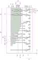
参考图8A,根据参考图7A至图7D描述的操作,可以形成在第二衬底215上的导电蚀刻停止层270、公共源极线层210、在公共源极线层210上的下牺牲层255、在下牺牲层255上的下支撑层260、在下支撑层260上的初步堆叠结构PS、穿透初步堆叠结构PS的沟道结构240(参见图7D)、在第二衬底215上的第二绝缘结构的第三部分IL2c、以及在第三绝缘结构的第二部分IL2c和初步堆叠结构PS上的第二绝缘结构的第二部分IL2b。根据不同的实施例,第一虚设沟道结构280(参考图7E)可以不形成,可以形成为具有与沟道结构240相同的结构,或者可以形成为如图7E所示。初步堆叠结构PS可以包括交替堆叠在下支撑层260上的多个层间绝缘层220和多个牺牲层235。Referring to FIG. 8A, according to the operations described with reference to FIGS. 7A to 7D, a conductive
在一些实施例中,初步堆叠结构PS的阶梯区域EXT可以根据上面参考图7A至图7D描述的操作被图案化以具有阶梯形状。层间绝缘层220可以是图7B至图7D所示的层间绝缘层220a和220b,并且牺牲层235可以是图7B至图7D所示的第一牺牲层235a和第二牺牲层235b。In some embodiments, the step region EXT of the preliminary stack structure PS may be patterned to have a step shape according to the operations described above with reference to FIGS. 7A to 7D . The interlayer insulating
参考图8B,可以形成穿透下支撑层260、初步堆叠结构PS和第二绝缘结构的第二部分IL2b并暴露下牺牲层255的的字线切口WSH和虚设字线切口DWSH。Referring to FIG. 8B , a word line cutout WSH and a dummy word line cutout DWSH that penetrate the
参考图8C,间隔物层SP可以形成在字线切口WSH的内壁上和虚设字线切口DWSH的内壁上。例如,间隔物层SP可以形成在字线切口WSH的内壁和底表面上,形成在虚设字线切口DWSH的内壁和底表面上,以及形成在第二绝缘结构的第二部分IL2b的顶表面上,并且间隔物层SP在字线切口WSH和虚设字线切口DWSH的底表面上以及在第二绝缘结构的第二部分IL2b的顶表面上的部分可以通过各向异性蚀刻间隔物层SP来去除。Referring to FIG. 8C , a spacer layer SP may be formed on inner walls of the word line cutouts WSH and on inner walls of the dummy word line cutouts DWSH. For example, the spacer layer SP may be formed on the inner wall and bottom surface of the word line cutout WSH, on the inner wall and bottom surface of the dummy word line cutout DWSH, and on the top surface of the second portion IL2b of the second insulating structure. , and the portion of the spacer layer SP on the bottom surface of the word line cutout WSH and the dummy word line cutout DWSH and on the top surface of the second portion IL2b of the second insulating structure may be removed by anisotropically etching the spacer layer SP .
一起参考图8C和图8D,可以去除下牺牲层255。如图7G所示,可以蚀刻栅极绝缘层241以暴露沟道层242。接下来,通过去除下牺牲层255形成的空间可以被下导电层250填充。接下来,可以从字线切口WSH和虚设字线切口DWSH的内壁去除间隔物层SP。接下来,可以通过去除牺牲层235来形成层间绝缘层220之间的多个空间235H。Referring to FIGS. 8C and 8D together, the lower
一起参考图8D和图8E,多个栅极层230可以填充层间绝缘层220之间的空间235H。以这种方式,可以完成包括交替堆叠在下支撑层260上的栅极层230和层间绝缘层220的堆叠结构SS。Referring to FIGS. 8D and 8E together, a plurality of gate layers 230 may fill
参考图8F,填充层WSF和虚设填充层DWSF可以分别填充字线切口WSH和虚设字线切口DWSH。在一些实施例中,填充层WSF和虚设填充层DWSF可以包括多晶硅。Referring to FIG. 8F , the filling layer WSF and the dummy filling layer DWSF may fill the word line slit WSH and the dummy word line slit DWSH, respectively. In some embodiments, the filling layer WSF and the dummy filling layer DWSF may include polysilicon.
一起参考图8F和图8G,从字线切口WSH中去除填充层WSF。为了防止虚设填充层DWSF被去除,可以在去除填充层WSF之前形成覆盖虚设填充层DWSF并暴露填充层WSF的掩模。可以在去除填充层WSF之后去除掩模。在去除填充层WSF之后,字线切口结构WS可以形成在字线切口WSH中。Referring to FIG. 8F and FIG. 8G together, the filling layer WSF is removed from the word line cutout WSH. In order to prevent the dummy filling layer DWSF from being removed, a mask covering the dummy filling layer DWSF and exposing the filling layer WSF may be formed before removing the filling layer WSF. The mask may be removed after removing the filling layer WSF. After the filling layer WSF is removed, the word line cutout structure WS may be formed in the word line cutout WSH.
参考图8G和图8H,从虚设字线切口DWSH中去除虚设填充层DWSF。接下来,绝缘层DWSb可以形成在虚设字线切口DWSH的内壁上。例如,绝缘层DWSb可以形成在虚设字线切口DWSH的内壁和底表面上,并且在一些实施例中,形成在第二绝缘结构的第二部分IL2b的顶表面上,然后可以通过各向异性蚀刻绝缘层DWSb来去除绝缘层DWSb在虚设字线切口DWSH的底表面上和第二绝缘结构的第二部分IL2b的顶表面上的部分。接下来,可以在绝缘层DWSb上形成导电层DWSa。导电层DWSa可以与绝缘层DWSb一起填充虚没字线切口DWSH。Referring to FIGS. 8G and 8H , the dummy filling layer DWSF is removed from the dummy word line cutout DWSH. Next, an insulating layer DWSb may be formed on the inner wall of the dummy word line cutout DWSH. For example, the insulating layer DWSb may be formed on the inner wall and bottom surface of the dummy word line cutout DWSH, and in some embodiments, on the top surface of the second portion IL2b of the second insulating structure, and then may be formed by anisotropic etching. The insulating layer DWSb is removed to remove portions of the insulating layer DWSb on the bottom surface of the dummy word line cutout DWSH and on the top surface of the second portion IL2b of the second insulating structure. Next, a conductive layer DWSa may be formed on the insulating layer DWSb. The conductive layer DWSa may fill the dummy word line cutout DWSH together with the insulating layer DWSb.
参考图8I,可以形成第二绝缘结构的第一部分IL2a、第二互连结构IC2和第二接合焊盘BP2。以这种方式,可以完成包括第一部分IL2a、第二部分IL2b和第三部分IL2c的第二绝缘结构IL2。Referring to FIG. 8I, the first portion IL2a of the second insulation structure, the second interconnection structure IC2, and the second bonding pad BP2 may be formed. In this way, the second insulating structure IL2 including the first portion IL2a, the second portion IL2b, and the third portion IL2c may be completed.
参考图8J连同图6和图8I,将图8I的结果结构倒置并接合到图6所示的第一结构S1上。Referring to FIG. 8J in conjunction with FIGS. 6 and 8I , the resulting structure of FIG. 8I is inverted and bonded to the first structure S1 shown in FIG. 6 .
一起参考图8J和图8K,可以去除第二衬底215以暴露导电蚀刻停止层270和第二绝缘结构IL2,从而完成接合到第一结构S1上的第二结构S2。在去除第二衬底215之后,导电蚀刻停止层270的顶表面可以在第一竖直高度LV1处(例如,设置在第一竖直高度LV1处),并且第二绝缘结构IL2的顶表面可以在比第一竖直高度LV1低的第二竖直高度LV2处。第二绝缘结构IL2的顶表面可以在比导电蚀刻停止层270的顶表面所位于的第三竖直高度LV3高的第二竖直高度LV2处。因此,即使在去除第二衬底215之后,公共源极线层210也可以被第二绝缘结构IL2覆盖而不暴露。Referring to FIGS. 8J and 8K together, the
参考图8L,形成覆盖第二绝缘结构IL2和导电蚀刻停止层270的第三绝缘结构IL3、穿透第三绝缘结构IL3的输入/输出通孔292、以及设置在第三绝缘结构IL3上并连接到输入/输出通孔292的输入/输出焊盘294。Referring to FIG. 8L, a third insulating structure IL3 covering the second insulating structure IL2 and the conductive
此后,可以形成图5B所示的第四绝缘结构IL4和外部连接焊盘296,从而形成非易失性存储器件100A。Thereafter, the fourth insulating structure IL4 and the
图9是根据本发明构思的示例实施例的包括非易失性存储器件的存储系统的示意图。FIG. 9 is a schematic diagram of a memory system including a nonvolatile memory device according to example embodiments of the inventive concepts. Referring to FIG.
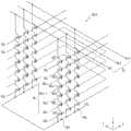
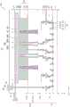
参考图9,存储系统1000可以包括一个或多个存储器件1100和电连接到一个或多个存储器件1100的存储控制器1200。存储系统1000可以是例如固态驱动器(SSD)设备、通用串行总线(USB)、计算系统、医疗设备或包括至少一个存储器件1100的通信设备。Referring to FIG. 9 , a
存储器件1100可以是非易失性存储器件。例如,存储器件1100可以是包括上面参考图4A至图5B描述的非易失性存储器件100和100A之一或其组合的NAND闪存器件。存储器件1100可以包括第一结构1100F和设置在第一结构1100F上的第二结构1100S。第一结构1100F可以对应于图4A和图5B所示的第一结构S1。图4A和图5B所述的外围电路PC可以包括行解码器1110、页缓冲器1120和逻辑电路1130。The
第二结构1100S可以对应于图4A和图5B所示的第二结构S2和S2A。第二结构1100S可以包括多条位线BL、公共源极线CSL、多条字线WL、第一串选择线UL1和第二串选择线UL2、第一地选择线LL1和第二地选择线LL2、以及位线BL和公共源极线CSL之间的存储单元串CSTR。图4A和图5B所示的第二互连结构IC2可以包括位线BL、字线WL、串选择线UL1和UL2以及地选择线LL1和LL2。图4A和图5B所示的沟道结构240和栅极层230a、230b和230可以构成存储单元串CSTR。图4A和图5B所示的公共源极线层210和导电蚀刻停止层270可以对应于公共源极线CSL。The
在第二结构1100S中,存储单元串CSTR均可以包括与公共源极线CSL相邻的地选择晶体管LT1和LT2、与位线BL相邻的串选择晶体管UT1和UT2、以及在地选择晶体管LT1和LT2以及串选择晶体管UT1和UT2之间的多个存储单元晶体管MCT。地选择晶体管LT1和LT2的数量以及串选择晶体管UT1和UT2的数量可以根据实施例进行不同地改变。图4A和图5B所示的沟道结构240以及栅极层230a、230b和230中的一个栅极层可以构成晶体管LT1、LT2、UT1、UT2和MCT中的一个。In the
在示例实施例中,第一地选择线LL1和第二地选择线LL2可以分别连接到地选择晶体管LT1和LT2的栅电极。字线WL可以连接到存储单元晶体管MCT的栅电极。第一串选择线UL1和第二串选择线UL2可以分别连接到串选择晶体管UT1和UT2的栅电极。In example embodiments, the first ground selection line LL1 and the second ground selection line LL2 may be connected to gate electrodes of the ground selection transistors LT1 and LT2, respectively. The word line WL may be connected to the gate electrode of the memory cell transistor MCT. The first and second string selection lines UL1 and UL2 may be connected to gate electrodes of the string selection transistors UT1 and UT2, respectively.
公共源极线CSL、地选择线LL1和LL2、字线WL以及第一串选择线UL1和第二串选择线UL2可以连接到行解码器1110。位线BL可以电连接到页缓冲器1120。A common source line CSL, ground selection lines LL1 and LL2 , a word line WL, and first and second string selection lines UL1 and UL2 may be connected to the
存储器件1100可以通过电连接到逻辑电路1130的外部连接焊盘1101与存储控制器1200通信。外部连接焊盘1101可以电连接到逻辑电路1130。外部连接焊盘1101可以是图4A和图5B所示的输入/输出焊盘294或外部连接焊盘296。The
存储控制器1200可以包括处理器1210、NAND控制器1220和主机接口1230。在一些实施例中,存储系统1000可以包括多个存储器件1100。在这种情况下,存储控制器1200可以控制存储器件1100。The
处理器1210可以控制存储系统1000的整体操作,包括存储控制器1200的操作。处理器1210可以根据固件进行操作,并且可以通过控制NAND控制器1220来访问存储器件1100。NAND控制器1220可以包括处理与存储器件1100的通信的NAND接口1221。用于控制存储器件1100的控制命令、要写入存储器件1100的存储单元晶体管MCT的数据、以及要从存储器件1100的存储单元晶体管MCT读取的数据可以通过NAND接口1221发送。主机接口1230可以提供存储系统1000和外部主机之间的通信功能。当通过主机接口1230从外部主机接收到控制命令时,处理器1210可以响应于控制命令来控制存储器件1100。The
图10是根据本发明构思的示例实施例的包括非易失性存储器件的存储系统的示意性透视图。FIG. 10 is a schematic perspective view of a memory system including a nonvolatile memory device according to example embodiments of the inventive concepts.
参考图10,根据本发明构思的示例实施例的存储系统2000包括主衬底2001、安装在主衬底2001上的存储控制器2002、一个或多个半导体封装2003,并且可以包括DRAM2004。半导体封装2003和DRAM 2004可以通过形成在主衬底2001上的多个布线图案2005连接到存储控制器2002。Referring to FIG. 10 , a
主衬底2001可以包括连接器2006,该连接器2006包括被配置为耦合到外部主机的多个引脚。连接器2006的引脚的数量和布置可以根据存储系统2000和外部主机之间的通信接口而变化。在示例实施例中,存储系统2000可以根据包括通用串行总线(USB)、外围组件互连快速(PCI-Express)、串行高级技术附件(SATA)、用于通用闪存存储(UFS)的M-Phy等的接口中的任何一个来与外部主机进行通信。在示例实施例中,存储系统2000可以通过经由连接器2006从外部主机供应的电力来操作。存储系统2000还可以包括将从外部主机供应的电力分配给存储控制器2002和半导体封装2003的电源管理集成电路(PMIC)。The
存储控制器2002可以向半导体封装2003写入数据或从半导体封装2003读取数据并且可以提高存储系统2000的操作速度。The
DRAM 2004可以是用于减轻作为数据存储空间的半导体封装2003与外部主机之间的速度差异的缓冲存储器。包括在存储系统2000中的DRAM 2004也可以作为一种高速缓冲存储器操作并且可以在半导体封装2003的控制操作中提供用于临时存储数据的空间。当DRAM 2004被包括在存储系统2000中时,除了用于控制半导体封装2003的NAND控制器之外,存储控制器2002还可以包括用于控制DRAM 2004的DRAM控制器。The
半导体封装2003可以包括彼此间隔开的第一半导体封装2003a和第二半导体封装2003b。第一半导体封装2003a和第二半导体封装2003b均可以是包括多个半导体芯片2200的半导体封装。第一半导体封装件2003a和第二半导体封装件2003a均可以包括封装衬底2100、设置在封装衬底2100上的半导体芯片2200、设置在每个半导体芯片2200的底表面上的粘合层2300、电连接半导体芯片2200和封装衬底2100的连接结构2400、以及覆盖封装衬底2100上的半导体芯片2200和连接结构2400的模塑层2500。The
封装衬底2100可以是包括多个封装上焊盘2130的印刷电路板。半导体芯片2200均可以包括输入/输出焊盘2210。输入/输出焊盘2210可以对应于图4A和图5B的输入/输出焊盘294或外部连接焊盘296。半导体芯片2200均可以包括参考图4A至图5B描述的非易失性存储器件100和100A中的至少一个、或具有来自非易失性存储器件100和/或100A的特征的组合的非易失性存储器件。The
在示例实施例中,连接结构2400可以是电连接输入/输出焊盘2210和封装上焊盘2130的接合线。因此,在第一半导体封装2003a和第二半导体封装2003b中,半导体芯片2200可以通过接合线彼此电连接并且可以电连接到封装衬底2100的封装上焊盘2130。在示例实施例中,在第一半导体封装2003a和第二半导体封装2003b中,半导体芯片2200可以通过包括硅通孔(TSV)的连接结构(代替包括接合线的连接结构2400或者除了包括接合线的连接结构2400之外)彼此连接。In example embodiments, the
在示例实施例中,存储控制器2002和半导体芯片2200可以被包括在一个封装中。在示例实施例中,存储控制器2002和半导体芯片2200可以安装在与主衬底2001不同的单独的插入衬底上,并且在这种情况下,存储控制器2002和半导体芯片2200可以通过形成在插入衬底上的布线彼此连接。In example embodiments, the
图11是根据本发明构思的示例实施例的半导体封装的示意性截面图。FIG. 11 is a schematic cross-sectional view of a semiconductor package according to example embodiments of the inventive concepts.
参考图11,在半导体封装2003中,封装衬底2100可以是印刷电路板。封装衬底2100可以包括封装衬底本体2120、布置在封装衬底本体2120的顶表面上的多个封装上焊盘2130(参见图10)、布置或暴露在封装衬底本体2120的底表面上的多个封装下焊盘2125、以及在封装衬底本体2120内部电连接封装上焊盘2130(参见图10)和封装下焊盘2125的多条内部导线2135。如图10所示,封装上焊盘2130可以电连接到连接结构2400。下焊盘2125可以通过多个导电凸块2800连接到图10所示的存储系统2000的主衬底2001上的布线图案2005。半导体芯片2200均可以包括如参考4A至图5B所描述的非易失性存储器件100和100A或者来自其的特征。Referring to FIG. 11, in a
因此,本发明构思的实施例提供了一种非易失性存储器件,其不需要单独的公共源极线接触或旁路结构来防止电荷在公共源极线中的积累。以这种方式,根据本公开的非易失性存储器件可以具有减小的平面区域、简化的制造工艺和提高的可靠性。Accordingly, embodiments of the inventive concept provide a nonvolatile memory device that does not require a separate common source line contact or bypass structure to prevent charge accumulation in the common source line. In this way, a nonvolatile memory device according to the present disclosure may have a reduced planar area, a simplified manufacturing process, and improved reliability.
尽管已经参照本发明构思的实施例具体示出并描述了本发明构思,但是将会理解,在不脱离所附权利要求书的精神和范围的情况下,可以在其中进行形式和细节上的各种改变。While the inventive concept has been particularly shown and described with reference to embodiments thereof, it will be understood that changes in form and details may be made therein without departing from the spirit and scope of the appended claims. kind of change.
Claims (20)
Translated fromChinese


Applications Claiming Priority (2)
| Application Number | Priority Date | Filing Date | Title |
|---|---|---|---|
| KR1020210138840AKR20230055284A (en) | 2021-10-18 | 2021-10-18 | Nonvolatile memory device, method of manufacturing the same, and memory system comprising the same |
| KR10-2021-0138840 | 2021-10-18 |
Publications (1)
| Publication Number | Publication Date |
|---|---|
| CN115996575Atrue CN115996575A (en) | 2023-04-21 |
Family
ID=85982549
Family Applications (1)
| Application Number | Title | Priority Date | Filing Date |
|---|---|---|---|
| CN202210996420.4APendingCN115996575A (en) | 2021-10-18 | 2022-08-18 | Nonvolatile memory device and memory system including the same |
Country Status (3)
| Country | Link |
|---|---|
| US (1) | US12278201B2 (en) |
| KR (1) | KR20230055284A (en) |
| CN (1) | CN115996575A (en) |
Families Citing this family (1)
| Publication number | Priority date | Publication date | Assignee | Title |
|---|---|---|---|---|
| JP7711019B2 (en)* | 2022-03-23 | 2025-07-22 | キオクシア株式会社 | Semiconductor memory device |
Family Cites Families (14)
| Publication number | Priority date | Publication date | Assignee | Title |
|---|---|---|---|---|
| KR101434588B1 (en) | 2008-06-11 | 2014-08-29 | 삼성전자주식회사 | Semiconductor device and manufacturing method thereof |
| KR102307487B1 (en) | 2014-06-23 | 2021-10-05 | 삼성전자주식회사 | Three-dimensional semiconductor memory device and method of fabricating the same |
| US9449987B1 (en) | 2015-08-21 | 2016-09-20 | Sandisk Technologies Llc | Three dimensional memory device with epitaxial semiconductor pedestal for peripheral transistors |
| KR102549967B1 (en) | 2017-11-21 | 2023-06-30 | 삼성전자주식회사 | Vertical memory devices and methods of manufacturing the same |
| US10916556B1 (en) | 2017-12-12 | 2021-02-09 | Sandisk Technologies Llc | Three-dimensional memory device using a buried source line with a thin semiconductor oxide tunneling layer |
| JP2019192663A (en) | 2018-04-18 | 2019-10-31 | 東芝メモリ株式会社 | Semiconductor memory |
| US10957648B2 (en) | 2018-07-20 | 2021-03-23 | Sandisk Technologies Llc | Three-dimensional memory device containing contact via structure extending through source contact layer and dielectric spacer assembly |
| KR102452827B1 (en) | 2018-09-13 | 2022-10-12 | 삼성전자주식회사 | Semiconductor device including contact plug |
| KR102650996B1 (en) | 2018-11-06 | 2024-03-26 | 삼성전자주식회사 | Semiconductor device |
| KR102705028B1 (en) | 2018-12-14 | 2024-09-10 | 삼성전자주식회사 | Three-dimensional semiconductor devices |
| CN111180344B (en) | 2020-01-02 | 2021-12-07 | 长江存储科技有限责任公司 | Three-dimensional stacked structure and preparation method |
| CN119364768A (en) | 2020-07-06 | 2025-01-24 | 长江存储科技有限责任公司 | Three-dimensional memory device and method for manufacturing the same |
| KR20220092087A (en)* | 2020-12-24 | 2022-07-01 | 삼성전자주식회사 | Semiconducotr device and electronic system including the same |
| KR20220169956A (en)* | 2021-06-21 | 2022-12-29 | 삼성전자주식회사 | Semiconductor devices and data storage systems including the same |
- 2021
- 2021-10-18KRKR1020210138840Apatent/KR20230055284A/enactivePending
- 2022
- 2022-05-26USUS17/825,076patent/US12278201B2/enactiveActive
- 2022-08-18CNCN202210996420.4Apatent/CN115996575A/enactivePending
Also Published As
| Publication number | Publication date |
|---|---|
| KR20230055284A (en) | 2023-04-25 |
| US12278201B2 (en) | 2025-04-15 |
| US20230117267A1 (en) | 2023-04-20 |
Similar Documents
| Publication | Publication Date | Title |
|---|---|---|
| US11967574B2 (en) | Memory device and data storage system including the same | |
| US11930638B2 (en) | Nonvolatile memory device and memory system comprising the same | |
| US20240429187A1 (en) | Integrated circuit device including peripheral circuit and cell array structures, and electronic system including same | |
| CN114582881A (en) | Nonvolatile memory device and data storage system including the same | |
| CN115996575A (en) | Nonvolatile memory device and memory system including the same | |
| US20240090240A1 (en) | Integrated circuit device | |
| EP4432807A1 (en) | Integrated circuit device and electronic system having the same | |
| EP4395492A1 (en) | Nonvolatile memory device | |
| US20250107098A1 (en) | Semiconductor devices and electronic systems including the same | |
| EP4391050A1 (en) | Chip stack structure and semiconductor package including the same | |
| US20250120089A1 (en) | Nonvolatile memory device and memory system including the same | |
| US20240389322A1 (en) | Non-volatile memory device and memory system including the same | |
| KR20230143067A (en) | Nonvolatile memory device and Method for Manufacturing the same | |
| KR20230175015A (en) | Integrated circuit device and electronic system having the same | |
| KR20250138534A (en) | Three-dimensional semiconductor memory device and electronic system including the same | |
| TW202442078A (en) | Non-volatile memory device and memory system including the same | |
| CN119815834A (en) | Nonvolatile memory device and electronic system including the same | |
| CN117425346A (en) | Semiconductor device with a semiconductor layer having a plurality of semiconductor layers | |
| CN117479540A (en) | Semiconductor device and electronic system including the same |
Legal Events
| Date | Code | Title | Description |
|---|---|---|---|
| PB01 | Publication | ||
| PB01 | Publication | ||
| SE01 | Entry into force of request for substantive examination | ||
| SE01 | Entry into force of request for substantive examination |