CN115987066A - A zero-current turn-on buck conversion system and method - Google Patents
A zero-current turn-on buck conversion system and methodDownload PDFInfo
- Publication number
- CN115987066A CN115987066ACN202310049736.7ACN202310049736ACN115987066ACN 115987066 ACN115987066 ACN 115987066ACN 202310049736 ACN202310049736 ACN 202310049736ACN 115987066 ACN115987066 ACN 115987066A
- Authority
- CN
- China
- Prior art keywords
- current
- voltage
- turn
- zero
- module
- Prior art date
- Legal status (The legal status is an assumption and is not a legal conclusion. Google has not performed a legal analysis and makes no representation as to the accuracy of the status listed.)
- Pending
Links
Images


Classifications
- Y—GENERAL TAGGING OF NEW TECHNOLOGICAL DEVELOPMENTS; GENERAL TAGGING OF CROSS-SECTIONAL TECHNOLOGIES SPANNING OVER SEVERAL SECTIONS OF THE IPC; TECHNICAL SUBJECTS COVERED BY FORMER USPC CROSS-REFERENCE ART COLLECTIONS [XRACs] AND DIGESTS
- Y02—TECHNOLOGIES OR APPLICATIONS FOR MITIGATION OR ADAPTATION AGAINST CLIMATE CHANGE
- Y02B—CLIMATE CHANGE MITIGATION TECHNOLOGIES RELATED TO BUILDINGS, e.g. HOUSING, HOUSE APPLIANCES OR RELATED END-USER APPLICATIONS
- Y02B70/00—Technologies for an efficient end-user side electric power management and consumption
- Y02B70/10—Technologies improving the efficiency by using switched-mode power supplies [SMPS], i.e. efficient power electronics conversion e.g. power factor correction or reduction of losses in power supplies or efficient standby modes
Landscapes
- Dc-Dc Converters (AREA)
Abstract
Description
Translated fromChinese技术领域technical field
本发明属于变换器技术领域,尤其涉及一种零电流开通BUCK变换系统及方法。The invention belongs to the technical field of converters, and in particular relates to a zero-current turn-on BUCK conversion system and method.
背景技术Background technique
目前,BUCK电路是把输入的高压经过变换器以后转换为较低的电压输出,和线性稳压电路相比而言,BUCK电路的体积更小,效率更高,是应用最广泛的电路之一。At present, the BUCK circuit converts the input high voltage into a lower voltage output after passing through the converter. Compared with the linear voltage regulator circuit, the BUCK circuit is smaller in size and higher in efficiency, and is one of the most widely used circuits. .
然而,在实际的使用过程中输入电压较高,输出电流比较大时,因其续流管的反向恢复导致上管在开通的时候其开通损耗很大,严重制了BUCK变换器的工作频率和效率。However, in the actual use process, when the input voltage is high and the output current is relatively large, the turn-on loss of the upper tube is very large when it is turned on due to the reverse recovery of the freewheeling tube, which seriously limits the operating frequency of the BUCK converter. and efficiency.
过高的反向恢复还会带来严重的EMC问题,以及减低了整个拓扑的可靠性,除反向恢复问题外,传统BUCK还存在最小占空比问题,即当输入电压较高时,BUCK以非常小占空比工作,输出电压也很高,当系统要求输出很低电压的时候,整个变换器只能进入间歇模式,这样会导致输出电流不连续,纹波加大。Excessive reverse recovery will also bring serious EMC problems and reduce the reliability of the entire topology. In addition to the reverse recovery problem, the traditional BUCK also has a minimum duty cycle problem, that is, when the input voltage is high, the BUCK Working with a very small duty cycle, the output voltage is also very high. When the system requires a very low output voltage, the entire converter can only enter the intermittent mode, which will cause discontinuous output current and increase the ripple.
通过上述分析,现有技术存在的问题及缺陷为:输入电压较高,输出电流比较大时,因其续流管的反向恢复导致上管在开通的时候其开通损耗很大,严重制了BUCK变换器的工作频率和效率。Through the above analysis, the problems and defects of the existing technology are: when the input voltage is high and the output current is relatively large, the turn-on loss of the upper tube is very large when it is turned on due to the reverse recovery of the freewheeling tube, which seriously affects the The operating frequency and efficiency of the BUCK converter.
发明内容Contents of the invention
针对现有技术存在的问题,本发明提供了一种零电流开通BUCK变换系统。Aiming at the problems existing in the prior art, the present invention provides a zero-current turn-on BUCK conversion system.
本发明是这样实现的,一种零电流开通BUCK变换方法包括一下步骤:The present invention is realized in this way, and a kind of zero-current opening BUCK conversion method comprises following steps:
步骤一:M1和M2断开,M3为续流状态,电流由M3的S级流向D级,此时D级电压为-1V;Step 1: M1 and M2 are disconnected, M3 is in the freewheeling state, and the current flows from the S level of M3 to the D level, and the voltage of the D level is -1V at this time;
步骤二:M1和M2同时开通,V8输入电压通过M1达到L5电感,M2导通以后M3的D级电压与L5右端电压相同为-1V;Step 2: M1 and M2 are turned on at the same time, the input voltage of V8 reaches the inductor of L5 through M1, and after M2 is turned on, the D-level voltage of M3 is the same as the voltage at the right end of L5, which is -1V;
步骤三:L5电感两端施加输入V8的全部电压,L5的电流由0开始上升,M3的续流电流大小开始降低,直到M3的续流电流变成0;Step 3: Apply the full voltage of the input V8 to both ends of the L5 inductor, the current of L5 starts to rise from 0, and the freewheeling current of M3 begins to decrease until the freewheeling current of M3 becomes 0;
步骤四:在VIN一定的情况下,L5的电感放电,M3实现电流的续流。Step 4: When VIN is constant, the inductance of L5 is discharged, and M3 realizes the continuous flow of current.
进一步,通过所述M1和M2同时开通时间D的计算L5的充电时长方法为:Further, the method of calculating the charging duration of L5 through the simultaneous turn-on time D of M1 and M2 is:
(1):计算加载在L5电感两端电压X,(1): Calculate the voltage X loaded on both ends of the L5 inductor,
X=(VIN-VOUT)*L5/(L5+L6),其中VIN为释放电压,VOUT为输出电压;X=(VIN-VOUT)*L5/(L5+L6), where VIN is the release voltage and VOUT is the output voltage;
(2):将VOUT在连续模式时,最大电压=VIN*D,带入到X得到,X=VIN*(1-D)*L5/(L5+L6);(2): When VOUT is in continuous mode, the maximum voltage = VIN*D, put it into X to get, X=VIN*(1-D)*L5/(L5+L6);
(3):L5充电时的伏秒Y1=D*VIN(1-D)*L5/(L5+L6)。(3): Volt-second Y1 when L5 is charging = D*VIN(1-D)*L5/(L5+L6).
进一步,所述L5的电感放电时间计算方法具体为:L5电感释放能量的时间最长为1-D,释放电压为VIN,电感释放时的伏秒Y2=(1-D)*VIN。Further, the calculation method of the inductance discharge time of L5 is specifically: the longest time for the L5 inductance to release energy is 1-D, the release voltage is VIN, and the volt-second Y2=(1-D)*VIN when the inductance is released.
进一步,所述一种零电流开通BUCK变换系统包括:Further, the zero-current turn-on BUCK conversion system includes:
输入电源模块;input power module;
输入电源模块线性连接第一功率模块和第二功率模块,第二功率模块线性连接输出电压模块。The input power module is linearly connected to the first power module and the second power module, and the second power module is linearly connected to the output voltage module.
进一步,所述输入电流模块设有V8,输入电源单元通过高频二极管单元连接第一功率模块和第二功率模块。Further, the input current module is provided with V8, and the input power supply unit is connected to the first power module and the second power module through a high-frequency diode unit.
进一步,所述第一功率模块设有第一功率管单元,第一功率管单元设有M1,M1线性连接V1单元。Further, the first power module is provided with a first power tube unit, and the first power tube unit is provided with M1, and M1 is linearly connected to the V1 unit.
进一步,所述V1单元设有V1,V1线性连接L5和D10。Further, the V1 unit is provided with V1, and V1 is linearly connected to L5 and D10.
进一步,所述第二功率模块设有第二功率管单元,第二功率管单元线性连接L6和第三功率管单元。Further, the second power module is provided with a second power tube unit, and the second power tube unit is linearly connected to L6 and the third power tube unit.
进一步,所述第二功率管单元设有M2,M2线性连接V2。Further, the second power tube unit is provided with M2, and M2 is linearly connected to V2.
进一步,所述第三功率管单元设有第三功率MOS管,第三功率MOS管线性连接M3。Further, the third power tube unit is provided with a third power MOS tube, and the third power MOS tube is linearly connected to M3.
进一步,所述L6线性连接输出电压模块,输出电压模块设有C7和VOUT。Further, the L6 is linearly connected to the output voltage module, and the output voltage module is provided with C7 and VOUT.
结合上述的技术方案和解决的技术问题,本发明所要保护的技术方案所具备的优点及积极效果为:Combining the above-mentioned technical solutions and technical problems to be solved, the advantages and positive effects of the technical solutions to be protected in the present invention are as follows:
第一、针对上述现有技术存在的技术问题以及解决该问题的难度,紧密结合本发明的所要保护的技术方案以及研发过程中结果和数据等,详细、深刻地分析本发明技术方案如何解决的技术问题,解决问题之后带来的一些具备创造性的技术效果。具体描述如下:First, in view of the technical problems existing in the above-mentioned prior art and the difficulty of solving the problems, closely combine the technical solution to be protected in the present invention and the results and data in the research and development process, etc., to analyze in detail and profoundly how to solve the technical solution of the present invention Technical problems, some creative technical effects brought about after solving the problems. The specific description is as follows:
本发明实施例通过设有输入电源模块线性连接第一功率模块和第二功率模块,第二功率模块线性连接输出电压模块,有效减低了续流管的反向恢复电流,使得开关管的开通功耗大幅下降,提高了整体变换器的效率,因其电流斜率变化缓慢,EMC特性会变好。In the embodiment of the present invention, the input power module is linearly connected to the first power module and the second power module, and the second power module is linearly connected to the output voltage module, which effectively reduces the reverse recovery current of the freewheeling tube and makes the turn-on work of the switch tube The power consumption is greatly reduced, and the efficiency of the overall converter is improved. Because the current slope changes slowly, the EMC characteristics will become better.
第二,把技术方案看做一个整体或者从产品的角度,本发明所要保护的技术方案具备的技术效果和优点,具体描述如下:Second, regarding the technical solution as a whole or from the perspective of a product, the technical effects and advantages of the technical solution to be protected by the present invention are specifically described as follows:
本发明实施例通过二级结构串联,当变换器中一颗功率管损坏击穿,输出端不至于瞬间输出高压,使得整个变换器可靠性大大提高,可用于高可靠性场合应用。The embodiments of the present invention are connected in series through the secondary structure. When a power tube in the converter is damaged and broken down, the output terminal will not output high voltage instantaneously, so that the reliability of the whole converter is greatly improved, and it can be used in high-reliability applications.
第三,作为本发明的权利要求的创造性辅助证据,还体现在以下几个重要方面:Third, as an auxiliary evidence of the inventiveness of the claims of the present invention, it is also reflected in the following important aspects:
(1)本发明的技术方案转化后的预期收益和商业价值为:(1) The expected income and commercial value after the conversion of the technical solution of the present invention are:
(2)本发明的技术方案填补了国内外业内技术空白:(2) The technical scheme of the present invention fills up the technological gap in the industry at home and abroad:
(3)本发明的技术方案是否解决了人们一直渴望解决、但始终未能获得成功的技术难题:(3) Whether the technical solution of the present invention has solved the technical problem that people have always been eager to solve but have not been able to achieve success:
(4)本发明的技术方案是否克服了技术偏见:。(4) Whether the technical solution of the present invention overcomes the technical prejudice:.
附图说明Description of drawings
图1是本发明实施例提供的零电流开通BUCK变换方法流程图;FIG. 1 is a flow chart of a zero-current turn-on BUCK conversion method provided by an embodiment of the present invention;
图2是本发明实施例提供的零电流开通BUCK变换原理图;FIG. 2 is a schematic diagram of zero-current turn-on BUCK conversion provided by an embodiment of the present invention;
图3是本发明实施例提供的第三高频二极管被短路数据图;FIG. 3 is a short-circuit data diagram of a third high-frequency diode provided by an embodiment of the present invention;
图4是本发明实施例提供的拓扑数据图。Fig. 4 is a topological data diagram provided by an embodiment of the present invention.
具体实施方式Detailed ways
为了使本发明的目的、技术方案及优点更加清楚明白,以下结合实施例,对本发明进行进一步详细说明。应当理解,此处所描述的具体实施例仅仅用以解释本发明,并不用于限定本发明。In order to make the object, technical solution and advantages of the present invention more clear, the present invention will be further described in detail below in conjunction with the examples. It should be understood that the specific embodiments described here are only used to explain the present invention, not to limit the present invention.
一、解释说明实施例。为了使本领域技术人员充分了解本发明如何具体实现,该部分是对权利要求技术方案进行展开说明的解释说明实施例。1. Explain the embodiment. In order to make those skilled in the art fully understand how to implement the present invention, this part is an explanatory embodiment for explaining the technical solution of the claims.
如图1-图2所示,本发明实施例提供的一种零电流开通BUCK变换方法包括一下步骤:As shown in Figure 1-Figure 2, a zero-current turn-on BUCK conversion method provided by an embodiment of the present invention includes the following steps:
S101:M1和M2断开,M3为续流状态,电流由M3的S级流向D级,此时D级电压为-1V;S101: M1 and M2 are disconnected, M3 is in the freewheeling state, the current flows from the S level of M3 to the D level, and the voltage of the D level is -1V at this time;
S102:M1和M2同时开通,V8输入电压通过M1达到L5电感,M2导通以后M3的D级电压与L5右端电压相同为-1V;S102: M1 and M2 are turned on at the same time, the input voltage of V8 reaches the inductor of L5 through M1, and after M2 is turned on, the D-level voltage of M3 is the same as the voltage at the right end of L5, which is -1V;
S103:L5电感两端施加输入V8的全部电压,L5的电流由0开始上升,M3的续流电流大小开始降低,直到M3的续流电流变成0;S103: The full voltage of the input V8 is applied to both ends of the L5 inductor, the current of L5 starts to rise from 0, and the freewheeling current of M3 begins to decrease until the freewheeling current of M3 becomes 0;
S104:在VIN一定的情况下,L5的电感放电,M3实现电流的续流。S104: When VIN is constant, the inductance of L5 is discharged, and M3 realizes the continuous flow of current.
通过所述M1和M2同时开通时间D的计算L5的充电时长方法为:The method of calculating the charging time of L5 through the simultaneous opening time D of M1 and M2 is:
(1):计算加载在L5电感两端电压X,(1): Calculate the voltage X loaded on both ends of the L5 inductor,
X=(VIN-VOUT)*L5/(L5+L6),其中VIN为释放电压,VOUT为输出电压;X=(VIN-VOUT)*L5/(L5+L6), where VIN is the release voltage and VOUT is the output voltage;
(2):将VOUT在连续模式时,最大电压=VIN*D,带入到X得到,X=VIN*(1-D)*L5/(L5+L6);(2): When VOUT is in continuous mode, the maximum voltage = VIN*D, put it into X to get, X=VIN*(1-D)*L5/(L5+L6);
(3):L5充电时的伏秒Y1=D*VIN(1-D)*L5/(L5+L6)。(3): Volt-second Y1 when L5 is charging = D*VIN(1-D)*L5/(L5+L6).
L5的电感放电时间计算方法具体为:L5电感释放能量的时间最长为1-D,释放电压为VIN,电感释放时的伏秒Y2=(1-D)*VIN。The calculation method of the inductor discharge time of L5 is specifically: the longest time for the L5 inductor to release energy is 1-D, the release voltage is VIN, and the volt-second Y2=(1-D)*VIN when the inductor releases.
一种零电流开通BUCK变换系统包括:A zero-current turn-on BUCK conversion system includes:
输入电源模块;input power module;
输入电源模块线性连接第一功率模块和第二功率模块,第二功率模块线性连接输出电压模块。The input power module is linearly connected to the first power module and the second power module, and the second power module is linearly connected to the output voltage module.
输入电流模块设有V8,输入电源单元通过高频二极管单元连接第一功率模块和第二功率模块。The input current module is provided with V8, and the input power supply unit is connected to the first power module and the second power module through a high-frequency diode unit.
第一功率模块设有第一功率管单元,第一功率管单元设有M1,M1线性连接V1单元。The first power module is provided with a first power tube unit, and the first power tube unit is provided with M1, and M1 is linearly connected to the V1 unit.
V1单元设有V1,V1线性连接L5和D10。Unit V1 is provided with V1, and V1 is linearly connected to L5 and D10.
第二功率模块设有第二功率管单元,第二功率管单元线性连接L6和第三功率管单元。The second power module is provided with a second power tube unit, and the second power tube unit is linearly connected to L6 and the third power tube unit.
第二功率管单元设有M2,M2线性连接V2。The second power tube unit is provided with M2, and M2 is linearly connected to V2.
第三功率管单元设有第三功率MOS管,第三功率MOS管线性连接M3。The third power tube unit is provided with a third power MOS tube, and the third power MOS tube is linearly connected to M3.
L6线性连接输出电压模块,输出电压模块设有C7和VOUT。L6 is linearly connected to the output voltage module, and the output voltage module is provided with C7 and VOUT.
二、应用实施例。为了证明本发明的技术方案的创造性和技术价值,该部分是对权利要求技术方案进行具体产品上或相关技术上的应用实施例。2. Application examples. In order to prove the creativity and technical value of the technical solution of the present invention, this part is the application example of the claimed technical solution on specific products or related technologies.
本发明实施例应用在BUCK电路中。The embodiment of the present invention is applied in a BUCK circuit.
三、实施例相关效果的证据。本发明实施例在研发或者使用过程中取得了一些积极效果,和现有技术相比的确具备很大的优势,下面内容结合试验过程的数据、图表等进行描述。3. Evidence of the relevant effects of the embodiment. The embodiment of the present invention has achieved some positive effects in the process of research and development or use, and indeed has great advantages compared with the prior art. The following content is described in conjunction with the data and charts of the test process.
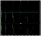
给原理图中的元器件添加适当参数,对比一下传统BUCK和我们的发明拓扑对管子开通电流的差异。Add appropriate parameters to the components in the schematic diagram, and compare the difference between the traditional BUCK and our inventive topology on the tube turn-on current.
①如图3所示,当原理图D12被短路时,第一级MOS不起作用,也就是传统BUCK电路,测量M2和M3功率管的开通电流大小。① As shown in Figure 3, when the schematic diagram D12 is short-circuited, the first-stage MOS does not work, that is, the traditional BUCK circuit, and measures the turn-on current of the M2 and M3 power tubes.
以L6电感电流大小作为参考,在L6电感平均电流20A时,M2开通电流约为34A,M3开通电流为18A左右。Taking the L6 inductor current as a reference, when the average current of the L6 inductor is 20A, the turn-on current of M2 is about 34A, and the turn-on current of M3 is about 18A.
②如图4所示,采用本发明的拓扑,同样以L6电感电流大小作为参考,在L6电感平均电流20A时,M2开通电流约为24A,M3开通电流为3.4A左右。②As shown in Figure 4, using the topology of the present invention, and taking the L6 inductor current as a reference, when the average current of the L6 inductor is 20A, the on-current of M2 is about 24A, and the on-current of M3 is about 3.4A.
以上所述,仅为本发明的具体实施方式,但本发明的保护范围并不局限于此,任何熟悉本技术领域的技术人员在本发明揭露的技术范围内,凡在本发明的精神和原则之内所作的任何修改、等同替换和改进等,都应涵盖在本发明的保护范围之内。The above is only a specific embodiment of the present invention, but the scope of protection of the present invention is not limited thereto. Anyone familiar with the technical field within the technical scope disclosed in the present invention, whoever is within the spirit and principles of the present invention Any modifications, equivalent replacements and improvements made within shall fall within the protection scope of the present invention.
Claims (10)
Priority Applications (1)
| Application Number | Priority Date | Filing Date | Title |
|---|---|---|---|
| CN202310049736.7ACN115987066A (en) | 2023-02-01 | 2023-02-01 | A zero-current turn-on buck conversion system and method |
Applications Claiming Priority (1)
| Application Number | Priority Date | Filing Date | Title |
|---|---|---|---|
| CN202310049736.7ACN115987066A (en) | 2023-02-01 | 2023-02-01 | A zero-current turn-on buck conversion system and method |
Publications (1)
| Publication Number | Publication Date |
|---|---|
| CN115987066Atrue CN115987066A (en) | 2023-04-18 |
Family
ID=85959582
Family Applications (1)
| Application Number | Title | Priority Date | Filing Date |
|---|---|---|---|
| CN202310049736.7APendingCN115987066A (en) | 2023-02-01 | 2023-02-01 | A zero-current turn-on buck conversion system and method |
Country Status (1)
| Country | Link |
|---|---|
| CN (1) | CN115987066A (en) |
Citations (5)
| Publication number | Priority date | Publication date | Assignee | Title |
|---|---|---|---|---|
| JPH05304769A (en)* | 1991-07-23 | 1993-11-16 | Fujitsu Ltd | Voltage resonant converter |
| CN108199579A (en)* | 2018-01-08 | 2018-06-22 | 厦门大学 | A kind of high no-load voltage ratio Sofe Switch DC-DC buck converters with coupling inductance |
| CN109951081A (en)* | 2019-04-15 | 2019-06-28 | 江苏工程职业技术学院 | A kind of end Buck coupling inductance formula buck translation circuit and control method |
| CN113809920A (en)* | 2021-08-19 | 2021-12-17 | 广州金升阳科技有限公司 | BUCK converter control method |
| CN219875493U (en)* | 2023-02-01 | 2023-10-20 | 东儿科技重庆有限公司 | Zero-current turn-on BUCK converter |
- 2023
- 2023-02-01CNCN202310049736.7Apatent/CN115987066A/enactivePending
Patent Citations (5)
| Publication number | Priority date | Publication date | Assignee | Title |
|---|---|---|---|---|
| JPH05304769A (en)* | 1991-07-23 | 1993-11-16 | Fujitsu Ltd | Voltage resonant converter |
| CN108199579A (en)* | 2018-01-08 | 2018-06-22 | 厦门大学 | A kind of high no-load voltage ratio Sofe Switch DC-DC buck converters with coupling inductance |
| CN109951081A (en)* | 2019-04-15 | 2019-06-28 | 江苏工程职业技术学院 | A kind of end Buck coupling inductance formula buck translation circuit and control method |
| CN113809920A (en)* | 2021-08-19 | 2021-12-17 | 广州金升阳科技有限公司 | BUCK converter control method |
| CN219875493U (en)* | 2023-02-01 | 2023-10-20 | 东儿科技重庆有限公司 | Zero-current turn-on BUCK converter |
Similar Documents
| Publication | Publication Date | Title |
|---|---|---|
| CN201063541Y (en) | High-frequency highly effective boosting DC/DC converter | |
| CN103368394B (en) | A kind of efficient voltage reducing type DC-DC converter | |
| CN112583252B (en) | A high power density high gain converter and its control method | |
| CN221058190U (en) | High-gain direct current converter based on coupling inductance | |
| CN113224942A (en) | Non-isolated Buck-Boost bridgeless PFC converter system | |
| CN111740583B (en) | Modal switching method and circuit for single-period control in hybrid conduction mode | |
| CN113489308A (en) | Step-down power factor correction converter without input current dead zone and control method | |
| CN107171544A (en) | A kind of full digital full-bridge isolated single-phase single-grade PFC(PFC)Converter | |
| CN103269164B (en) | The quasi-single-stage high power factor circuit of former limit current constant control and device | |
| CN107612030B (en) | A Photovoltaic Converter with Quasi-Critical Continuous Current and Soft Switching of Devices | |
| CN113489309A (en) | Bridgeless buck power factor correction converter with wide output voltage and control method | |
| CN203352444U (en) | High-efficiency step-down DC-DC converter | |
| CN201805599U (en) | High power factor two-stage LED driver circuit without optocoupler | |
| CN219875493U (en) | Zero-current turn-on BUCK converter | |
| CN201417403Y (en) | Constant Power Control Device of Switching Power Supply | |
| CN203636178U (en) | Inverter welder | |
| CN106655862A (en) | Ripple suppressing non-isolated inverter and control method thereof | |
| CN115987066A (en) | A zero-current turn-on buck conversion system and method | |
| CN205847090U (en) | A hybrid quasi-switching step-up DC-DC converter | |
| CN118539738A (en) | Totem-pole PFC digital control method with multimode self-adaptive switching | |
| CN111555604A (en) | A Novel Quasi-Single-Stage High Power Factor Circuit | |
| CN112886817B (en) | A high-efficiency high-gain converter and its control method | |
| CN113726147B (en) | Input-parallel output series bridgeless buck PFC converter | |
| CN105978322A (en) | Switch capacitor type high-gain quasi Z source DC-DC converter | |
| CN114337264B (en) | Boost conversion circuit, device and method |
Legal Events
| Date | Code | Title | Description |
|---|---|---|---|
| PB01 | Publication | ||
| PB01 | Publication | ||
| SE01 | Entry into force of request for substantive examination | ||
| SE01 | Entry into force of request for substantive examination |