CN115986353A - Coaxial microstrip conversion structure - Google Patents
Coaxial microstrip conversion structureDownload PDFInfo
- Publication number
- CN115986353A CN115986353ACN202211740704.3ACN202211740704ACN115986353ACN 115986353 ACN115986353 ACN 115986353ACN 202211740704 ACN202211740704 ACN 202211740704ACN 115986353 ACN115986353 ACN 115986353A
- Authority
- CN
- China
- Prior art keywords
- coaxial
- insulator
- impedance
- microstrip
- microstrip line
- Prior art date
- Legal status (The legal status is an assumption and is not a legal conclusion. Google has not performed a legal analysis and makes no representation as to the accuracy of the status listed.)
- Pending
Links
Images


Landscapes
- Waveguide Aerials (AREA)
Abstract
Translated fromChinese
Description
Translated fromChinese技术领域technical field
本申请涉及微波毫米波射频技术领域,尤其涉及一种同轴微带转换结构。The present application relates to the field of microwave and millimeter wave radio frequency technologies, and in particular to a coaxial microstrip conversion structure.
背景技术Background technique
在毫米波系统中,射频模组之间的连接多采用同轴结构,同轴连接器和同轴电缆具有体积小、工作带宽大、传输路径可重塑等优势,广泛应用于毫米波系统中长距离传输。在射频模组内部,同轴连接器可通过射频绝缘子与微带电路连接。随着射频模组的发展,在追求高性能的同时,也需要进行小型化、轻量化设计。微带线是目前最流行的平面传输线,采用印制电路板实现,非常易与其他无源和有源毫米波器件集成,是微波毫米波混合集成电路的最佳媒介。毫米波射频电路,尤其是工作频率在10GHz以上频段,大量采用裸片形式的功能电路,如放大器、混频器、滤波器、移相器等。使用微组装工艺进行毫米波射频电路的高精度装配生产,从而实现很小的射频模组单元内,其射频路径上的裸芯片器件达几十个之多。这也对毫米波射频模组的端口驻波提出很大的挑战。目前难以做到超宽带匹配,设计出具有大工作带宽、低插入损耗、高传输效率等特点的同轴微带转换结构,是毫米波射频模组电路研制中重要一环。In the millimeter wave system, the connection between RF modules mostly adopts a coaxial structure. Coaxial connectors and coaxial cables have the advantages of small size, large working bandwidth, and reshapeable transmission paths, and are widely used in millimeter wave systems. Long distance transmission. Inside the RF module, the coaxial connector can be connected to the microstrip circuit through the RF insulator. With the development of RF modules, miniaturization and lightweight design are also required while pursuing high performance. Microstrip line is currently the most popular planar transmission line. It is realized by printed circuit board and is very easy to integrate with other passive and active millimeter wave devices. It is the best medium for microwave and millimeter wave hybrid integrated circuits. Millimeter wave radio frequency circuits, especially in the frequency band above 10GHz, use a large number of functional circuits in the form of bare chips, such as amplifiers, mixers, filters, phase shifters, etc. Micro-assembly technology is used for high-precision assembly and production of millimeter-wave radio frequency circuits, so that in a small radio frequency module unit, there are as many as dozens of bare chip devices on the radio frequency path. This also poses a great challenge to the port standing wave of the mmWave RF module. At present, it is difficult to achieve ultra-wideband matching. Designing a coaxial microstrip conversion structure with the characteristics of large operating bandwidth, low insertion loss, and high transmission efficiency is an important part of the development of millimeter-wave radio frequency module circuits.
发明内容Contents of the invention
本申请提供一种低损耗、超宽带、结构简单易加工的同轴微带转换结构。The application provides a coaxial microstrip conversion structure with low loss, ultra-broadband, simple structure and easy processing.
本申请提供一种同轴微带转换结构,包括:射频绝缘子、绝缘子探针、同轴空气腔、微带线和金属载体,所述微带线包括设于所述金属载体的微带线介质板和设于所述微带线介质板的阻抗渐变中心导体;所述射频绝缘子的一端与所述金属载体的一端侧壁齐平,所述射频绝缘子的另一端通过所述同轴空气腔定位于所述金属载体;所述绝缘子探针贯穿所述射频绝缘子的中心轴线,并在所述射频绝缘子的两端延伸,其中所述绝缘子探针的一端可连接至同轴连接器,所述绝缘子探针的另一端穿过所述同轴空气腔形成空气同轴,并搭接在所述微带线的所述阻抗渐变中心导体。The application provides a coaxial microstrip conversion structure, including: a radio frequency insulator, an insulator probe, a coaxial air cavity, a microstrip line and a metal carrier, and the microstrip line includes a microstrip line medium arranged on the metal carrier plate and the impedance gradient central conductor arranged on the microstrip dielectric plate; one end of the radio frequency insulator is flush with the side wall of one end of the metal carrier, and the other end of the radio frequency insulator is positioned through the coaxial air cavity on the metal carrier; the insulator probe runs through the central axis of the radio frequency insulator, and extends at both ends of the radio frequency insulator, wherein one end of the insulator probe can be connected to a coaxial connector, and the insulator The other end of the probe passes through the coaxial air cavity to form an air coaxial, and is connected to the impedance gradient center conductor of the microstrip line.
可选的,所述阻抗渐变中心导体包括阻抗渐变段和与所述阻抗渐变段连接的阻抗固定段,所述阻抗渐变段相对所述阻抗固定段靠近所述绝缘子探针设置,且所述阻抗渐变段与所述绝缘子探针搭接。Optionally, the impedance gradient central conductor includes an impedance gradient section and an impedance fixed section connected to the impedance gradient section, the impedance gradient section is arranged closer to the insulator probe relative to the impedance fixed section, and the impedance The transition section overlaps the insulator probe.
可选的,所述阻抗渐变段的阻抗大于所述阻抗固定段的阻抗,其中所述阻抗固定段的阻抗为50欧姆。Optionally, the impedance of the impedance gradient section is greater than the impedance of the impedance fixed section, wherein the impedance of the impedance fixed section is 50 ohms.
可选的,所述阻抗渐变中心导体相对靠近所述绝缘子探针的一端与所述同轴空气腔的侧壁之间具有间隙。Optionally, there is a gap between an end of the impedance gradient center conductor relatively close to the insulator probe and a side wall of the coaxial air cavity.
可选的,所述微带线介质板相对靠近所述绝缘子探针的一端与所述同轴空气腔的侧壁之间具有间隙。Optionally, there is a gap between an end of the microstrip line dielectric plate relatively close to the insulator probe and a side wall of the coaxial air cavity.
可选的,所述阻抗渐变中心导体的长度相对于所述微带线介质板的长度避让的尺寸范围为0.01mm~0.2mm。Optionally, the length of the impedance gradient center conductor is within a range of 0.01 mm to 0.2 mm relative to the length of the microstrip line dielectric plate.
可选的,所述阻抗渐变中心导体相对靠近所述绝缘子探针的一端与所述绝缘子探针焊接。Optionally, one end of the impedance gradient central conductor relatively close to the insulator probe is welded to the insulator probe.
可选的,所述微带线还包括底层金属层,设于所述微带线介质板的底部,所述微带线介质板通过所述底层金属层焊接于所述金属载体。Optionally, the microstrip line further includes a bottom metal layer disposed at the bottom of the microstrip line dielectric board, and the microstrip line dielectric board is welded to the metal carrier through the bottom metal layer.
可选的,所述微带线介质板为高频介质板。Optionally, the microstrip line dielectric board is a high-frequency dielectric board.
可选的,所述射频绝缘子的绝缘介质为玻璃材质。Optionally, the insulating medium of the radio frequency insulator is made of glass.
可选的,所述微带线为所述微带线介质板表面的覆铜带。Optionally, the microstrip line is a copper-clad strip on the surface of the microstrip line dielectric board.
本申请实施例的同轴微带转换结构,通过设置绝缘子探针穿过同轴空气腔形成空气同轴,并搭接在微带线的阻抗渐变中心导体上,可补偿由电磁波模式转变引入的失配、为满足装配工艺安全性和可靠性等引入的不连续所带来的失配,实现毫米波信号的高效率传输,以满足毫米波射频模组对端口转换的低损耗、超宽带、结构简单易加工等的需求。In the coaxial microstrip conversion structure of the embodiment of the present application, by setting the insulator probe through the coaxial air cavity to form an air coaxial, and lapped on the central conductor of the impedance gradient of the microstrip line, it can compensate for the electromagnetic wave mode change. Mismatch, the mismatch caused by the discontinuity introduced to meet the safety and reliability of the assembly process, etc., to achieve high-efficiency transmission of millimeter-wave signals to meet the low-loss, ultra-wideband, Requirements such as simple structure and easy processing.
附图说明Description of drawings
图1所示为本申请的同轴微带转换结构的一个实施例的结构示意图。FIG. 1 is a schematic structural diagram of an embodiment of the coaxial microstrip conversion structure of the present application.
图2所示为图1所示的同轴微带转换结构的一个视角的结构示意图。FIG. 2 is a structural schematic diagram of a perspective view of the coaxial microstrip conversion structure shown in FIG. 1 .
图3所示为图1所示的同轴微带转换结构的另一个视角的结构示意图。FIG. 3 is a structural schematic diagram of another viewing angle of the coaxial microstrip conversion structure shown in FIG. 1 .
图4所示为图1所示的同轴微带转换结构插入损耗的仿真结果图。FIG. 4 is a simulation result diagram of the insertion loss of the coaxial microstrip conversion structure shown in FIG. 1 .
图5所示为图1所示的同轴微带转换结构输入驻波的仿真结果图。FIG. 5 is a simulation result diagram of the input standing wave of the coaxial microstrip conversion structure shown in FIG. 1 .
具体实施方式Detailed ways
这里将详细地对示例性实施例进行说明,其示例表示在附图中。下面的描述涉及附图时,除非另有表示,不同附图中的相同数字表示相同或相似的要素。以下示例性实施例中所描述的实施方式并不代表与本申请相一致的所有实施方式。相反,它们仅是与如所附权利要求书中所详述的、本申请的一些方面相一致的装置的例子。Reference will now be made in detail to the exemplary embodiments, examples of which are illustrated in the accompanying drawings. When the following description refers to the accompanying drawings, the same numerals in different drawings refer to the same or similar elements unless otherwise indicated. The implementations described in the following exemplary embodiments do not represent all implementations consistent with this application. Rather, they are merely examples of means consistent with aspects of the present application as recited in the appended claims.
在本申请使用的术语是仅仅出于描述特定实施例的目的,而非旨在限制本申请。除非另作定义,本申请使用的技术术语或者科学术语应当为本发明所属领域内具有一般技能的人士所理解的通常意义。本申请说明书以及权利要求书中使用的“第一”“第二”以及类似的词语并不表示任何顺序、数量或者重要性,而只是用来区分不同的组成部分。同样,“一个”或者“一”等类似词语也不表示数量限制,而是表示存在至少一个。若仅指代“一个”时会再单独说明。“多个”或者“若干”表示两个及两个以上。除非另行指出,“前部”、“后部”、“下部”和/或“上部”等类似词语只是为了便于说明,而并非限于一个位置或者一种空间定向。“包括”或者“包含”等类似词语意指出现在“包括”或者“包含”前面的元件或者物件涵盖出现在“包括”或者“包含”后面列举的元件或者物件及其等同,并不排除其他元件或者物件。“连接”或者“相连”等类似的词语并非限定于物理的或者机械的连接,而且可以包括电性的连接,不管是直接的还是间接的。在本申请说明书和所附权利要求书中所使用的单数形式的“一种”、“所述”和“该”也旨在包括多数形式,除非上下文清楚地表示其他含义。还应当理解,本文中使用的术语“和/或”是指并包含一个或多个相关联的列出项目的任何或所有可能组合。The terminology used in this application is for the purpose of describing particular embodiments only, and is not intended to limit the application. Unless otherwise defined, the technical terms or scientific terms used in the present application shall have the common meanings understood by those skilled in the art to which the present invention belongs. "First", "second" and similar words used in the specification and claims of this application do not indicate any sequence, quantity or importance, but are only used to distinguish different components. Likewise, words like "a" or "one" do not denote a limitation in quantity, but indicate that there is at least one. If only "one" is referred to, it will be explained separately. "Multiple" or "several" means two or more. Unless otherwise indicated, terms such as "front", "rear", "lower" and/or "upper" are used for convenience of description only and are not intended to be limiting to a position or orientation in space. "Includes" or "comprises" and similar terms mean that the elements or items listed before "comprises" or "comprises" include the elements or items listed after "comprises" or "comprises" and their equivalents, and do not exclude other elements or objects. Words such as "connected" or "connected" are not limited to physical or mechanical connections, and may include electrical connections, whether direct or indirect. As used in this specification and the appended claims, the singular forms "a", "the" and "the" are also intended to include the plural forms unless the context clearly dictates otherwise. It should also be understood that the term "and/or" as used herein refers to and includes any and all possible combinations of one or more of the associated listed items.
毫米波信号在同轴微带转换结构中传输时,经历同轴传输线TEM模到50欧姆微带线准TEM模的转变,这其中还有微带线和金属载体侧壁间空气间隙、阻抗渐变中心导体避让、绝缘子探针焊接微带线等引入的不连续,其传输特性极易随着频率的升高而快速恶化。目前典型的同轴微带转换结构,其形式是加入同轴空气腔,与绝缘子探针形成空气同轴。该结构的一大限制是,引入的优化变量较少(同轴空气腔的半径和长度),难以做到超宽带匹配。设计出具有大工作带宽、低插入损耗、高传输效率等特点的同轴微带转换结构,是毫米波射频模组电路研制中重要一环。When the millimeter wave signal is transmitted in the coaxial microstrip conversion structure, it undergoes the transition from the TEM mode of the coaxial transmission line to the quasi-TEM mode of the 50 ohm microstrip line, which also includes air gaps and impedance gradients between the microstrip line and the sidewall of the metal carrier The discontinuity introduced by center conductor avoidance, insulator probe welding microstrip line, etc., its transmission characteristics are easy to deteriorate rapidly with the increase of frequency. The current typical coaxial microstrip conversion structure is in the form of adding a coaxial air cavity to form an air coaxial with the insulator probe. A major limitation of this structure is that there are few optimization variables introduced (radius and length of the coaxial air cavity), and it is difficult to achieve ultra-broadband matching. Designing a coaxial microstrip conversion structure with the characteristics of large operating bandwidth, low insertion loss, and high transmission efficiency is an important part of the development of millimeter-wave radio frequency module circuits.
因此,本申请提供一种低损耗、超宽带、结构简单易加工的同轴微带转换结构。同轴微带转换结构包括射频绝缘子、绝缘子探针、同轴空气腔、微带线和金属载体,微带线包括设于金属载体的微带线介质板和设于微带线介质板的阻抗渐变中心导体;射频绝缘子的一端与金属载体的一端侧壁齐平,射频绝缘子的另一端通过同轴空气腔定位于金属载体;绝缘子探针贯穿射频绝缘子的中心轴线,并在射频绝缘子的两端延伸,其中绝缘子探针的一端可连接至同轴连接器,绝缘子探针的另一端穿过同轴空气腔形成空气同轴,并搭接在微带线的阻抗渐变中心导体。如此设置,通过设置绝缘子探针穿过同轴空气腔搭接在微带线的阻抗渐变中心导体上,可补偿由电磁波模式转变引入的失配、为满足装配工艺安全性和可靠性等引入的不连续所带来的失配,实现毫米波信号的高效率传输,以满足毫米波射频模组对端口转换的低损耗、超宽带、结构简单易加工等的需求。Therefore, the present application provides a coaxial microstrip conversion structure with low loss, ultra-wideband, simple structure and easy processing. The coaxial microstrip conversion structure includes a radio frequency insulator, an insulator probe, a coaxial air cavity, a microstrip line and a metal carrier. Gradient central conductor; one end of the RF insulator is flush with the side wall of one end of the metal carrier, and the other end of the RF insulator is positioned on the metal carrier through a coaxial air cavity; the insulator probe runs through the central axis of the RF insulator and is placed at both ends of the RF insulator Extending, one end of the insulator probe can be connected to the coaxial connector, the other end of the insulator probe passes through the coaxial air cavity to form an air coaxial, and is lapped on the impedance gradient central conductor of the microstrip line. In such a setting, by setting the insulator probe through the coaxial air cavity and lapping it on the impedance gradient center conductor of the microstrip line, it can compensate the mismatch caused by the electromagnetic wave mode change and the safety and reliability of the assembly process. The mismatch caused by discontinuity realizes the high-efficiency transmission of millimeter wave signals to meet the needs of millimeter wave RF modules for port conversion with low loss, ultra-wideband, simple structure and easy processing.
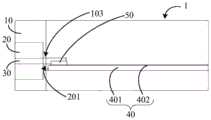
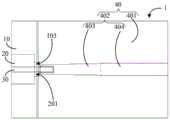
图1所示为本申请的同轴微带转换结构1的一个实施例的结构示意图。图2所示为图1所示的同轴微带转换结构1的一个视角的结构示意图。图3所示为图1所示的同轴微带转换结构1的另一个视角的结构示意图。结合图1至图3所示,同轴微带转换结构1包括射频绝缘子20、绝缘子探针30、同轴空气腔201、微带线40和金属载体10。其中,金属载体10作为固定载体,用于固定射频绝缘子20和微带线40。微带线40包括设于金属载体10的微带线介质板401和设FIG. 1 is a structural schematic diagram of an embodiment of a coaxial
于微带线介质板401的阻抗渐变中心导体402。射频绝缘子20的一端与金属载5体10的一端侧壁齐平,射频绝缘子20的另一端通过同轴空气腔201定位于金属载体10。绝缘子探针30贯穿射频绝缘子20的中心轴线,并在射频绝缘子20的两端延伸,其中绝缘子探针30的一端可连接至同轴连接器(未图示),绝缘子探针30的另一端穿过同轴空气腔201形成空气同轴,并搭接在微带线40的阻抗渐变中心导体402。The impedance
0在图1所示的实施例中,绝缘子探针30穿设于射频绝缘子20。绝缘子探针30的中心轴线与射频绝缘子20的中心轴线同轴设置。绝缘子探针30相对靠近微带线40的一端与同轴空气腔201形成空气同轴,并穿过同轴空气腔201延伸至射频绝缘子20外。阻抗渐变中心导体402相对靠近绝缘子探针30的一端与0 In the embodiment shown in FIG. 1 , the
绝缘子探针30连接。绝缘子探针30贯穿射频绝缘子20的中心轴线,并在射频5绝缘子20的两端延伸。在一些实施例中,绝缘子探针30可延伸至射频绝缘子20的左侧,与2.92mm的同轴连接器连接。绝缘子探针30可延伸至射频绝缘子20的右侧,穿过同轴空气腔201搭接在阻抗渐变中心导体402上,并与阻抗渐变中心导体402连接。在本实施例中,射频绝缘子20的左端与金属载体10的The
左侧壁齐平,射频绝缘子20的右端通过同轴空气腔201定位,烧结在绝缘孔1030上。同轴微带转换结构1工作时,毫米波信号经射频绝缘子20、绝缘子探针30The left side wall is flush, and the right end of the
与同轴空气腔201组成的空气同轴、搭接至阻抗渐变中心导体402上。其中绝缘子探针30与同轴空气腔201组成的空气同轴、阻抗渐变中心导体402起到阻抗匹配作用。如此可降低插入损耗,改善驻波。可补偿由电磁波模式转变引入The air formed by the
的失配、为满足装配工艺安全性和可靠性等引入的不连续所带来的失配,实现5毫米波信号的高效率传输,以满足毫米波射频模组对端口转换的低损耗、超宽The mismatch caused by the discontinuity introduced to meet the safety and reliability of the assembly process, etc., to achieve high-efficiency transmission of 5 mm wave signals to meet the requirements of low loss and ultra- Width
带、结构简单易加工等的需求。belt, simple structure and easy processing.
在图1至图3所示的实施例中,微带线介质板401为高频介质板。高频介质板为复合纤维材料板,型号为Rogers5880,厚度为0.254mm,介电常数为2.2。在图1至图3所示的实施例中,射频绝缘子20的绝缘介质为玻璃材质。在图1至图3所示的实施例中,金属载体10为镀金合金材质。在一些实施例中,金属载体10为镀金铝合金材质或镀金铜合金材质或镀银合金材质,但不仅限于此。在图1至图3所示的实施例中,微带线为微带线介质板401表面的覆铜带。在图1至图3所示的实施例中,射频绝缘子20的外表面镀有金层或锡层或银层,与金属载体10连接。在图1至图3所示的实施例中,绝缘子探针30的外表面镀有金层或锡层或银层,与阻抗渐变中心导体402连接。在本实施例中,射频绝缘子20的绝缘介质为Glass7070,介电常数为4.1,射频绝缘子20的直径为1.93mm,绝缘子探针30的直径为0.3mm,射频绝缘子20和绝缘子探针30的外表面均镀有金层,便于进行射频绝缘子20与金属载体10、绝缘子探针30与阻抗渐变中心导体402的焊接。使用时可依据射频绝缘子20的公差尺寸精度进行设计,以降低由装配引入的不连续性。In the embodiments shown in FIG. 1 to FIG. 3 , the microstrip line
在图1至图3所示的实施例中,阻抗渐变中心导体402包括阻抗渐变段403和与阻抗渐变段403连接的阻抗固定段404,阻抗渐变段403相对阻抗固定段404靠近绝缘子探针30设置,且阻抗渐变段403与绝缘子探针30搭接。在图1至图3所示的实施例中,阻抗渐变段403的阻抗大于阻抗固定段404的阻抗,其中阻抗固定段404的阻抗为50欧姆。同轴微带转换结构1工作时,毫米波信号经射频绝缘子20、绝缘子探针30与同轴空气腔201组成的空气同轴、搭接至阻抗渐变中心导体402上的绝缘子探针30、阻抗渐变中心导体402的阻抗渐变段403,传输至50欧姆阻抗固定段404上,其中绝缘子探针30与同轴空气腔201组成的空气同轴、微带线阻抗渐变段起到阻抗匹配作用。如此设置,引入同轴空气腔201和阻抗渐变中心导体402的阻抗渐变段403进行阻抗匹配,引入更多的优化变量,以实现超宽带毫米波信号高效传输。In the embodiment shown in FIGS. 1 to 3 , the impedance gradient
在图1至图3所示的实施例中,阻抗渐变中心导体402相对靠近绝缘子探针30的一端与同轴空气腔201的侧壁之间具有间隙。如此设置,在充分考虑装配工艺安全性和可靠性需求,避免或减少阻抗渐变中心导体402在射频绝缘子20焊接或绝缘子探针30焊接时易发生短路的情形。因此,将阻抗渐变中心导体402相对靠近绝缘子探针30的一端与同轴空气腔201的侧壁之间设有足够的余量的间隙来避让,安全可靠。In the embodiment shown in FIG. 1 to FIG. 3 , there is a gap between the end of the impedance
在图1至图3所示的实施例中,微带线介质板401相对靠近绝缘子探针30的一端与同轴空气腔201的侧壁之间具有间隙。在一些实施例中,微带线介质板401相对靠近绝缘子探针30的一端距离同轴空气腔201的侧壁之间的尺寸范围为0.05mm~0.1mm。在一些实施例中,微带线介质板401相对靠近绝缘子探针30的一端距离同轴空气腔201的侧壁之间的尺寸为0.05mm或0.06mm或0.07mm或0.08mm或0.09mm或0.1mm。如此设置,在充分考虑装配工艺安全性和可靠性需求,避免或减少因微带线介质板401超出金属载体10的尺寸难以安装的情况发生,且避免或减少微带线介质板401与金属载体10发生短路的情况发生。因此,将微带线介质板401相对靠近绝缘子探针30的一端与同轴空气腔201的侧壁之间设有足够的余量的间隙来避让,安全可靠。In the embodiment shown in FIGS. 1 to 3 , there is a gap between the end of the microstrip line
在图1至图3所示的实施例中,阻抗渐变中心导体402的长度相对于微带线介质板401的长度避让的尺寸范围为0.01mm~0.2mm。在一些实施例中,阻抗渐变中心导体402的长度相对于微带线介质板401的长度避让的尺寸为0.01mm或0.02mm或0.03mm或0.04mm或0.05mm或0.06mm或0.07mm或0.08mm或0.09mm或0.1mm或0.11mm或0.12mm或0.13mm或0.14mm或0.15mm或0.16mm或0.17mm或0.18mm或0.19mm或0.2mm。如此设置,为满足装配工艺安全性和可靠性的需求,降低装配过程中引入的短路风险。且该结构紧凑,工作频带宽,调试量小、可重复性高,适用于毫米波工程应用,可以广泛满足实际工程需求。In the embodiments shown in FIG. 1 to FIG. 3 , the length of the impedance
在图1至图3所示的实施例中,阻抗渐变中心导体402相对靠近绝缘子探针30的一端与绝缘子探针30焊接。在本实施例中,阻抗渐变中心导体402相对靠近绝缘子探针30的一端与绝缘子探针30通过锡焊50焊接。通过焊接方式连接阻抗渐变中心导体402和绝缘子探针30,连接稳定性更好。In the embodiment shown in FIG. 1 to FIG. 3 , one end of the impedance
在图1至图3所示的实施例中,微带线40还包括底层金属层(未图示),设于微带线介质板401的底部,微带线介质板401通过底层金属层焊接于金属载体10。微带线介质板401通过底层金属层焊接于金属载体10,固定效果稳定,且连接性能稳定可靠。In the embodiment shown in Figures 1 to 3, the
图4所示为图1所示的同轴微带转换结构1插入损耗的仿真结果图。在图4所示的实施例中,工作频率在50GHz时,插入损耗为-0.6648dB。图5所示为图1所示的同轴微带转换结构1输入驻波的仿真结果图。在图5所示的实施例中,工作频率在50GHz时,输入驻波比为1.1971。如此设置,通过设置绝缘子探针30穿过同轴空气腔201搭接在微带线40的阻抗渐变中心导体402上,可补偿由电磁波模式转变引入的失配、为满足装配工艺安全性和可靠性等引入的不连续所带来的失配,实现毫米波信号的高效率传输,以满足毫米波射频模组对端口转换的低损耗、超宽带、结构简单易加工等的需求。FIG. 4 is a simulation result diagram of the insertion loss of the coaxial
以上所述仅为本申请的较佳实施例而已,并不用以限制本申请,凡在本申请的精神和原则之内,所做的任何修改、等同替换、改进等,均应包含在本申请保护的范围之内。The above is only a preferred embodiment of the application, and is not intended to limit the application. Any modifications, equivalent replacements, improvements, etc. made within the spirit and principles of the application should be included in the application. within the scope of protection.
Claims (10)
Translated fromChinesePriority Applications (1)
| Application Number | Priority Date | Filing Date | Title |
|---|---|---|---|
| CN202211740704.3ACN115986353A (en) | 2022-12-30 | 2022-12-30 | Coaxial microstrip conversion structure |
Applications Claiming Priority (1)
| Application Number | Priority Date | Filing Date | Title |
|---|---|---|---|
| CN202211740704.3ACN115986353A (en) | 2022-12-30 | 2022-12-30 | Coaxial microstrip conversion structure |
Publications (1)
| Publication Number | Publication Date |
|---|---|
| CN115986353Atrue CN115986353A (en) | 2023-04-18 |
Family
ID=85967822
Family Applications (1)
| Application Number | Title | Priority Date | Filing Date |
|---|---|---|---|
| CN202211740704.3APendingCN115986353A (en) | 2022-12-30 | 2022-12-30 | Coaxial microstrip conversion structure |
Country Status (1)
| Country | Link |
|---|---|
| CN (1) | CN115986353A (en) |
Cited By (1)
| Publication number | Priority date | Publication date | Assignee | Title |
|---|---|---|---|---|
| CN117728138A (en)* | 2023-12-26 | 2024-03-19 | 北京信芯科技有限公司 | Welding-free connecting mechanism of coaxial connector and planar microstrip |
Citations (8)
| Publication number | Priority date | Publication date | Assignee | Title |
|---|---|---|---|---|
| JPH02237301A (en)* | 1989-03-10 | 1990-09-19 | Nec Corp | Coaxial microstrip line converter |
| JP2008219476A (en)* | 2007-03-05 | 2008-09-18 | Mitsubishi Electric Corp | Transmission line converter, high-frequency circuit and high-frequency module having the same |
| CN102569949A (en)* | 2010-12-09 | 2012-07-11 | 中国航天科工集团第二研究院二十三所 | Millimeter-wave band microstrip-coaxial line conversion device |
| CN206921989U (en)* | 2017-06-30 | 2018-01-23 | 成都玖信科技有限公司 | A kind of transition connector of glass insulator and microstrip line |
| CN107681240A (en)* | 2016-08-02 | 2018-02-09 | 北京遥感设备研究所 | A kind of coaxial microband conversion equipment |
| CN110676551A (en)* | 2019-09-23 | 2020-01-10 | 博微太赫兹信息科技有限公司 | Microstrip coaxial conversion structure with air cavity and interconnection method thereof |
| CN112599946A (en)* | 2020-12-22 | 2021-04-02 | 上海创远仪器技术股份有限公司 | Device for realizing millimeter wave frequency band microstrip coaxial conversion |
| CN114142198A (en)* | 2021-12-16 | 2022-03-04 | 西安梅隆控制工程有限责任公司 | Single leakage cable with multipath effect and construction method |
- 2022
- 2022-12-30CNCN202211740704.3Apatent/CN115986353A/enactivePending
Patent Citations (8)
| Publication number | Priority date | Publication date | Assignee | Title |
|---|---|---|---|---|
| JPH02237301A (en)* | 1989-03-10 | 1990-09-19 | Nec Corp | Coaxial microstrip line converter |
| JP2008219476A (en)* | 2007-03-05 | 2008-09-18 | Mitsubishi Electric Corp | Transmission line converter, high-frequency circuit and high-frequency module having the same |
| CN102569949A (en)* | 2010-12-09 | 2012-07-11 | 中国航天科工集团第二研究院二十三所 | Millimeter-wave band microstrip-coaxial line conversion device |
| CN107681240A (en)* | 2016-08-02 | 2018-02-09 | 北京遥感设备研究所 | A kind of coaxial microband conversion equipment |
| CN206921989U (en)* | 2017-06-30 | 2018-01-23 | 成都玖信科技有限公司 | A kind of transition connector of glass insulator and microstrip line |
| CN110676551A (en)* | 2019-09-23 | 2020-01-10 | 博微太赫兹信息科技有限公司 | Microstrip coaxial conversion structure with air cavity and interconnection method thereof |
| CN112599946A (en)* | 2020-12-22 | 2021-04-02 | 上海创远仪器技术股份有限公司 | Device for realizing millimeter wave frequency band microstrip coaxial conversion |
| CN114142198A (en)* | 2021-12-16 | 2022-03-04 | 西安梅隆控制工程有限责任公司 | Single leakage cable with multipath effect and construction method |
Cited By (2)
| Publication number | Priority date | Publication date | Assignee | Title |
|---|---|---|---|---|
| CN117728138A (en)* | 2023-12-26 | 2024-03-19 | 北京信芯科技有限公司 | Welding-free connecting mechanism of coaxial connector and planar microstrip |
| CN117728138B (en)* | 2023-12-26 | 2024-07-23 | 北京信芯科技有限公司 | Welding-free connecting mechanism of coaxial connector and planar microstrip |
Similar Documents
| Publication | Publication Date | Title |
|---|---|---|
| CN205666315U (en) | Be used for W wave band waveguide - microstrip probe converter | |
| CN101496279B (en) | Transitions device | |
| CN108711665A (en) | Rectangular waveguide micro-strip hermetic seal transition circuit | |
| CN103579729B (en) | A kind of spaceborne high-frequency microstrip is to the vertical change-over circuit of waveguide broad-band filter with low insertion loss | |
| CN112382837B (en) | Waveguide-microstrip conversion structure in form of end-connected capacitor arc probe | |
| CN113363691B (en) | Radio frequency substrate and coaxial microstrip conversion structure | |
| CN105977595A (en) | Terminal connection feed-backward type rectangular waveguide-microstrip transition device | |
| KR20120078697A (en) | Precision waveguide interface | |
| CN107689475B (en) | A micro-coaxial ultra-wideband coupler | |
| WO2013077916A1 (en) | High frequency, high bandwidth, low loss microstrip to waveguide transition | |
| CN114464975A (en) | Surface mount waveguide for vertical transition of printed circuit boards | |
| WO2020014891A1 (en) | Balun and method for manufacturing the same | |
| CN118920056A (en) | Gold wire bonding matching structure and method for interconnecting coplanar waveguide and chip microstrip | |
| CN107134620B (en) | A K-band waveguide microstrip transition device | |
| CN115986353A (en) | Coaxial microstrip conversion structure | |
| CN107275735A (en) | A kind of new coaxial microband converter | |
| CN112018067A (en) | BGA ceramic vertical interconnection structure and package based on broadband transmission | |
| CN204885390U (en) | A double-layer miniaturized low-cost directional branch coupler | |
| CN116325346A (en) | RF connector | |
| CN117650352A (en) | W-band waveguide port metal-ceramic shell | |
| CN113889719B (en) | Waveguide-microstrip line transition structure with filtering function | |
| CN216698694U (en) | Millimeter wave waveguide coaxial microstrip conversion structure | |
| CN214378786U (en) | Waveguide-to-strip line transition structure | |
| CN120237391A (en) | A system on a chip | |
| CN110011002B (en) | Self-matching ultra-wideband microwave insulator |
Legal Events
| Date | Code | Title | Description |
|---|---|---|---|
| PB01 | Publication | ||
| PB01 | Publication | ||
| SE01 | Entry into force of request for substantive examination | ||
| SE01 | Entry into force of request for substantive examination |