CN115981565A - Memory, data storage method and electronic device - Google Patents
Memory, data storage method and electronic deviceDownload PDFInfo
- Publication number
- CN115981565A CN115981565ACN202211731504.1ACN202211731504ACN115981565ACN 115981565 ACN115981565 ACN 115981565ACN 202211731504 ACN202211731504 ACN 202211731504ACN 115981565 ACN115981565 ACN 115981565A
- Authority
- CN
- China
- Prior art keywords
- memory
- data
- cache
- flash memory
- cache area
- Prior art date
- Legal status (The legal status is an assumption and is not a legal conclusion. Google has not performed a legal analysis and makes no representation as to the accuracy of the status listed.)
- Pending
Links
- 230000015654memoryEffects0.000titleclaimsabstractdescription146
- 238000000034methodMethods0.000titleclaimsabstractdescription46
- 238000013500data storageMethods0.000titleclaimsabstractdescription33
- 238000013507mappingMethods0.000claimsdescription7
- 238000004891communicationMethods0.000description10
- 230000006870functionEffects0.000description9
- 238000010586diagramMethods0.000description7
- 230000008569processEffects0.000description6
- 230000008901benefitEffects0.000description5
- 230000001360synchronised effectEffects0.000description5
- 230000007423decreaseEffects0.000description3
- 230000000694effectsEffects0.000description2
- 230000007334memory performanceEffects0.000description2
- 238000012545processingMethods0.000description2
- 230000003068static effectEffects0.000description2
- 238000012546transferMethods0.000description2
- 241000699670Mus sp.Species0.000description1
- 230000005540biological transmissionEffects0.000description1
- 238000004590computer programMethods0.000description1
- 230000036541healthEffects0.000description1
- 230000003862health statusEffects0.000description1
- 239000004973liquid crystal related substanceSubstances0.000description1
- 238000012544monitoring processMethods0.000description1
- 230000009467reductionEffects0.000description1
Images


Classifications
- Y—GENERAL TAGGING OF NEW TECHNOLOGICAL DEVELOPMENTS; GENERAL TAGGING OF CROSS-SECTIONAL TECHNOLOGIES SPANNING OVER SEVERAL SECTIONS OF THE IPC; TECHNICAL SUBJECTS COVERED BY FORMER USPC CROSS-REFERENCE ART COLLECTIONS [XRACs] AND DIGESTS
- Y02—TECHNOLOGIES OR APPLICATIONS FOR MITIGATION OR ADAPTATION AGAINST CLIMATE CHANGE
- Y02D—CLIMATE CHANGE MITIGATION TECHNOLOGIES IN INFORMATION AND COMMUNICATION TECHNOLOGIES [ICT], I.E. INFORMATION AND COMMUNICATION TECHNOLOGIES AIMING AT THE REDUCTION OF THEIR OWN ENERGY USE
- Y02D10/00—Energy efficient computing, e.g. low power processors, power management or thermal management
Landscapes
- Techniques For Improving Reliability Of Storages (AREA)
Abstract
Description
Translated fromChinese技术领域technical field
本申请属于数据存储技术领域,具体涉及一种存储器、数据存储方法及电子设备。The present application belongs to the technical field of data storage, and in particular relates to a memory, a data storage method and electronic equipment.
背景技术Background technique
当前,随着人们使用手机场景的丰富,人们对手机存储容量的要求也越高,但同时期望在不会增加成本的情况下,性能以及寿命等可靠性指标也能够满足应用的需求。在存储器不断的迭代升级过程中,实现了更大的存储容量以及单位存储成本降低。At present, as people use mobile phones in more and more scenarios, people have higher requirements for mobile phone storage capacity, but at the same time, it is expected that reliability indicators such as performance and lifespan can also meet the needs of applications without increasing costs. In the process of continuous iterative upgrading of the memory, greater storage capacity and unit storage cost reduction have been achieved.
但是,存储器的迭代升级也使得存储器的性能以及寿命等可靠性指标不断下降,从而难以满足在不同情况下用户对数据存储的需求。However, the iterative upgrade of the memory also makes the reliability indicators such as the performance and life of the memory continuously decrease, making it difficult to meet the user's demand for data storage in different situations.
发明内容Contents of the invention
本申请实施例提供一种存储器、数据存储方法及电子设备,能够解决存储器的迭代升级导致的存储器性能以及寿命等可靠性指标下降的问题。Embodiments of the present application provide a memory, a data storage method, and an electronic device, which can solve the problem of a decrease in reliability indicators such as memory performance and service life caused by iterative upgrades of the memory.
第一方面,本申请实施例提供了一种存储器,该存储器包括:主机、动态随机存取存储器(Dynamic Random Access Memory,DRAM)和通用闪存存储器(Universal FlashStorage,UFS);其中,所述UFS包括:控制器和非易失性闪存器(NAND),其中,所述控制器包括:第一缓存区域,所述第一缓存区域的存储单元为随机存取存储单元(Random AccessMemory,RAM);所述NAND包括:第二缓存区域,所述第二缓存区域的存储单元为单层级单元(Single Level Cell,SLC);所述DRAM包括:用于NAND数据读写的第三缓存区域,其中,所述第三缓存区域的存储单元为RAM。In the first aspect, the embodiment of the present application provides a memory, which includes: a host, a dynamic random access memory (Dynamic Random Access Memory, DRAM) and a universal flash memory (Universal Flash Storage, UFS); wherein, the UFS includes : a controller and a non-volatile flash memory (NAND), wherein the controller includes: a first cache area, the storage unit of the first cache area is a random access memory unit (Random AccessMemory, RAM); Said NAND comprises: the second cache area, and the storage unit of said second cache area is a single level unit (Single Level Cell, SLC); Described DRAM comprises: the 3rd cache area for NAND data reading and writing, wherein, The storage unit of the third cache area is RAM.
第二方面,本申请实施例提供了一种数据存储方法,该方法包括:获取待存储数据;根据存储器设置的存储模式,确定所述待存储数据存储的目标缓存模块,其中,所述存储模式包括以下之一:高可靠模式、高容量模式以及标准模式,不同存储模式对应的缓存模块不完全相同;将所述待存储数据存储到所述目标缓存模块;其中,所述存储器包括如第一方面所述的存储器。In a second aspect, an embodiment of the present application provides a data storage method, the method comprising: acquiring data to be stored; determining a target cache module for storing the data to be stored according to a storage mode set by the memory, wherein the storage mode Including one of the following: high-reliability mode, high-capacity mode and standard mode, the cache modules corresponding to different storage modes are not completely the same; the data to be stored is stored in the target cache module; wherein, the memory includes the first aspects of memory.
第三方面,本申请实施例提供了一种电子设备,该电子设备包括处理器、存储器及存储在所述存储器上并可在所述处理器上运行的程序或指令,所述程序或指令被所述处理器执行时实现如第二方面所述的方法的步骤。In a third aspect, an embodiment of the present application provides an electronic device, the electronic device includes a processor, a memory, and a program or instruction stored in the memory and operable on the processor, and the program or instruction is The processor implements the steps of the method described in the second aspect when executed.
第四方面,本申请实施例提供了一种芯片,所述芯片包括处理器和通信接口,所述通信接口和所述处理器耦合,所述处理器用于运行程序或指令,实现如第二方面所述的方法。In a fourth aspect, an embodiment of the present application provides a chip, the chip includes a processor and a communication interface, the communication interface is coupled to the processor, and the processor is used to run programs or instructions, so as to implement the second aspect the method described.
在本申请实施例中,通过获取待存储数据;根据存储器设置的存储模式,确定所述待存储数据存储的目标缓存模块,其中,所述存储模式包括以下之一:高可靠模式、高容量模式以及标准模式,不同存储模式对应的缓存模块不完全相同;将所述待存储数据存储到所述目标缓存模块;其中,所述存储器包括如第一方面所述的存储器,提供了多种存储模式可供选择,能够解决存储器的迭代升级导致的存储器性能以及寿命等可靠性指标下降的问题,并且能够满足在不同情况下用户对数据存储的需求。In the embodiment of the present application, by obtaining the data to be stored; according to the storage mode set by the memory, the target cache module for storing the data to be stored is determined, wherein the storage mode includes one of the following: high reliability mode, high capacity mode As well as the standard mode, the cache modules corresponding to different storage modes are not exactly the same; the data to be stored is stored in the target cache module; wherein, the memory includes the memory as described in the first aspect, providing multiple storage modes As an option, it can solve the problem of memory performance and reliability index decline caused by iterative upgrade of the memory, and can meet the user's demand for data storage in different situations.
附图说明Description of drawings
图1是本申请实施例提供的一种存储器的的结构示意图;FIG. 1 is a schematic structural diagram of a memory provided by an embodiment of the present application;
图2是本申请实施例提供的一种数据存储方法的流程示意图;FIG. 2 is a schematic flow diagram of a data storage method provided by an embodiment of the present application;
图3是本申请实施例提供的一种地址映射关系的示意图;FIG. 3 is a schematic diagram of an address mapping relationship provided by an embodiment of the present application;
图4是本申请实施例提供的另一种数据存储方法的流程示意图;Fig. 4 is a schematic flow chart of another data storage method provided by the embodiment of the present application;
图5是本申请实施例提供的一种用户操作界面的示意图;Fig. 5 is a schematic diagram of a user operation interface provided by an embodiment of the present application;
图6是本申请实施例提供的一种电子设备的结构示意图。FIG. 6 is a schematic structural diagram of an electronic device provided by an embodiment of the present application.
具体实施方式Detailed ways
下面将结合本申请实施例中的附图,对本申请实施例中的技术方案进行清楚、完整地描述,显然,所描述的实施例是本申请一部分实施例,而不是全部的实施例。基于本申请中的实施例,本领域普通技术人员在没有作出创造性劳动前提下所获得的所有其他实施例,都属于本申请保护的范围。The following will clearly and completely describe the technical solutions in the embodiments of the present application with reference to the drawings in the embodiments of the present application. Obviously, the described embodiments are part of the embodiments of the present application, not all of them. Based on the embodiments in this application, all other embodiments obtained by persons of ordinary skill in the art without creative efforts fall within the protection scope of this application.
本申请的说明书和权利要求书中的术语“第一”、“第二”等是用于区别类似的对象,而不用于描述特定的顺序或先后次序。应该理解这样使用的数据在适当情况下可以互换,以便本申请的实施例能够以除了在这里图示或描述的那些以外的顺序实施,且“第一”、“第二”等所区分的对象通常为一类,并不限定对象的个数,例如第一对象可以是一个,也可以是多个。此外,说明书以及权利要求中“和/或”表示所连接对象的至少其中之一,字符“/”,一般表示前后关联对象是一种“或”的关系。The terms "first", "second" and the like in the specification and claims of the present application are used to distinguish similar objects, and are not used to describe a specific sequence or sequence. It should be understood that the terms so used are interchangeable under appropriate circumstances such that the embodiments of the application can be practiced in sequences other than those illustrated or described herein, and that references to "first," "second," etc. distinguish Objects are generally of one type, and the number of objects is not limited. For example, there may be one or more first objects. In addition, "and/or" in the specification and claims means at least one of the connected objects, and the character "/" generally means that the related objects are an "or" relationship.
下面结合附图,通过具体的实施例及其应用场景对本申请实施例提供的存储器、数据存储方法及电子设备进行详细地说明。The memory, the data storage method, and the electronic device provided by the embodiments of the present application will be described in detail below through specific embodiments and application scenarios with reference to the accompanying drawings.
图1示出本申请的一个实施例提供的一种存储器的结构示意图,参照图1,该存储器100可以包括:主机101、DRAM 102和UFS 103;其中,所述UFS 103包括:控制器1031和NAND1032,其中,所述控制器1031包括:第一缓存区域10311,所述第一缓存区域10311的存储单元为RAM;所述NAND 1032包括:第二缓存区域10322,所述第二缓存区域10322的存储单元为SLC;所述DRAM 102包括:用于NAND 1032数据读写的第三缓存区域1021,其中,所述第三缓存区域1021的存储单元为RAM。FIG. 1 shows a schematic structural diagram of a memory provided by an embodiment of the present application. Referring to FIG. 1, the
本申请实施例提供的存储器100通过主机101进行系统任务的调度分配,例如在进行数据存储时对缓存区域的分配,并且主机101能够与DRAM 102和UFS 103之间进行信息以及指令传输;UFS 103属于系统内存,进行系统以及用户数据的存储,包括控制器1031和NAND 1032,控制器1031与主机101进行通信以及对NAND 1032进行管理;控制器1031包括存储单元为RAM的第一缓存单元10311,NAND 1032包括存储单元为SLC的第二缓存区域10322;DRAM 102属于系统内存,在系统运行时进行数据以及程序指令的存取,包括用于NAND1032数据读写的第三缓存区域1021,而且RAM具有随时读写且速度快的特点以及SLC具有速度快且寿命长的特点,利用了DRAM 102高性能且寿命长的特点,为数据存储提供了较好的存储条件。The
图2示出本申请的一个实施例提供的一种数据存储方法的流程示意图,该方法可以由电子设备执行,该电子设备可以包括:终端设备,其中终端设备可以例如车载终端或手机终端等。参照图2,该方法可以包括如下步骤:FIG. 2 shows a schematic flowchart of a data storage method provided by an embodiment of the present application. The method may be executed by an electronic device, and the electronic device may include: a terminal device, where the terminal device may be, for example, a vehicle-mounted terminal or a mobile phone terminal. Referring to Figure 2, the method may include the following steps:
步骤201:获取待存储数据;Step 201: Obtain data to be stored;
步骤202:根据存储器设置的存储模式,确定所述待存储数据存储的目标缓存模块,其中,所述存储模式包括以下之一:高可靠模式、高容量模式以及标准模式,不同存储模式对应的缓存模块不完全相同;Step 202: Determine the target cache module for storing the data to be stored according to the storage mode set by the memory, wherein the storage mode includes one of the following: high-reliability mode, high-capacity mode, and standard mode, and caches corresponding to different storage modes The modules are not identical;
步骤203:将所述待存储数据存储到所述目标缓存模块;其中,所述存储器包括如权利要求1所述的存储器。Step 203: Store the data to be stored in the target cache module; wherein the memory comprises the memory according to claim 1.
其中,高可靠模式提供更优的性能以及更长的寿命;高容量模式提供更大的存储空间。Among them, the high-reliability mode provides better performance and longer life; the high-capacity mode provides larger storage space.
在本申请实施例中,获取到待存储数据后,根据当前存储器设置的存储模式,确定待存储数据将要存储的目标缓存模块,例如当前设置的存储模式为高可靠模式则确定其对应的目标缓存模块,将待存储数据存储到高可靠模式对应的目标缓存模块,从而提升数据存储的性能、寿命等可靠性指标;当前设置的存储模式为高容量模式则确定其对应的目标缓存模块,将待存储数据存储到高容量模式对应的目标缓存模块,获取扩大的数据存储空间;当前设置的存储模式为标准模式则确定我对应的目标缓存模块,将待存储数据存储到标准模式对应的目标缓存模块;通过设置的不同的存储模式,由于使用的目标存储模块所具有的特点能够提升数据存储的性能、寿命等可靠性指标,也能够满足用户在不同情况下对数据存储的需求。In the embodiment of the present application, after obtaining the data to be stored, according to the storage mode set by the current memory, determine the target cache module where the data to be stored will be stored. For example, if the currently set storage mode is a high-reliability mode, then determine its corresponding target cache module, which stores the data to be stored in the target cache module corresponding to the high-reliability mode, so as to improve the reliability indicators such as data storage performance and lifespan; if the currently set storage mode is high-capacity mode, determine its corresponding target cache Store data in the target cache module corresponding to the high-capacity mode to obtain expanded data storage space; if the currently set storage mode is the standard mode, determine the corresponding target cache module, and store the data to be stored in the target cache module corresponding to the standard mode ; By setting different storage modes, due to the characteristics of the target storage module used, the reliability indicators such as data storage performance and life can be improved, and it can also meet the needs of users for data storage in different situations.
在一种实现方式中,存储器的存储模式可以由用户从电子设备的设置菜单栏“运存与存储空间”设置存储模式,如图5所示;存储器的存储模式也可以通过自动监控存储器的健康状况,基于存储器的健康状况,例如通过监测存储单元的擦写磨损次数,在设定条件下切换为高可靠模式或高容量模式或标准模式;并且可以增加存储模式的切换提醒功能,用于提醒用户存储器的存储模式发生切换。In one implementation, the storage mode of the memory can be set by the user from the setting menu bar "storage and storage space" of the electronic device, as shown in Figure 5; the storage mode of the memory can also be automatically monitored by the health of the memory Status, based on the health status of the memory, for example, by monitoring the number of erasing and writing wear of the storage unit, switch to the high-reliability mode or high-capacity mode or standard mode under the set conditions; and the switching reminder function of the storage mode can be added to remind The storage mode of the user memory is switched.
在一种实现方式中,上述的步骤202可以包括以下步骤:In an implementation manner, the
步骤301:确定所述存储器设置的存储模式为高可靠模式;Step 301: Determine that the storage mode set by the memory is a high-reliability mode;
步骤302:在所述存储器的UFS的NAND的第二缓存区域存在可用的存储空间的情况下,确定所述目标缓存模块为所述第二缓存区域。Step 302: If there is available storage space in the second cache area of the NAND of the UFS of the memory, determine that the target cache module is the second cache area.
在本申请实施例中,确定存储器的存储模式为高可靠模式时,在该存储器的UFS的NAND的第二缓存区域存在可用的存储空间的情况下,将该第二缓存区域确定为目标缓存模块,即在待存储数据的数据量小于当前第二缓存区域可用的存储空间时,将待存储数据暂时存储在第二缓存区域,不转存于NAND,以此提升数据存储的性能以及减少对NAND的寿命损耗。In the embodiment of the present application, when it is determined that the storage mode of the memory is a high-reliability mode, if there is available storage space in the second cache area of the UFS NAND of the memory, the second cache area is determined as the target cache module , that is, when the amount of data to be stored is less than the storage space currently available in the second cache area, the data to be stored is temporarily stored in the second cache area and not transferred to NAND, so as to improve the performance of data storage and reduce the impact on NAND loss of life.
在一种实现方式中,在上述步骤302之后还可以包括步骤303:在所述存储器的UFS的NAND的第二缓存区域没有可用的存储空间、且所述存储器的UFS的控制器的第一缓存区域存在可用的存储空间的情况下,确定所述目标缓存模块为所述第一缓存区域。In one implementation, step 303 may also be included after the above step 302: there is no available storage space in the second cache area of the UFS NAND of the memory, and the first cache of the UFS controller of the memory If there is available storage space in the region, determine that the target cache module is the first cache region.
在本申请实施例中,在存储器的存储模式为高可靠模式时,存储器的UFS的NAND的第二缓存区域已经存储数据没有可用的存储空间,并且该存储器的UFS的控制器的第一缓存区域存在可用的存储空间的情况下,将该第一缓存区域确定为目标缓存模块,将待存储数据存储到第一缓存区域,为待存储数据提供存储空间,能够进行数据的存储。In this embodiment of the application, when the storage mode of the memory is the high-reliability mode, the second cache area of the NAND of the UFS of the memory has stored data and there is no available storage space, and the first cache area of the controller of the UFS of the memory If there is available storage space, determine the first cache area as the target cache module, store the data to be stored in the first cache area, provide storage space for the data to be stored, and store the data.
在一种实现方式中,在上述步骤303之后还可以包括步骤304:在所述存储器的UFS的NAND的第二缓存区域没有可用的存储空间、且所述存储器的UFS的控制器的第一缓存区域也没有可用的存储空间的情况下,确定所述目标缓存模块为所述存储器的DRAM的第三缓存区域。In one implementation, step 304 may also be included after the above step 303: there is no available storage space in the second cache area of the UFS NAND of the memory, and the first cache of the UFS controller of the memory If there is no available storage space in the region, it is determined that the target cache module is the third cache region of the DRAM of the memory.
在本申请实施例中,在存储器的存储模式为高可靠模式时,用于存储数据的第一缓存区域与第二缓存区域均已没有可用的存储空间的情况下,将还未存5储数据的第三缓存区域确定为目标缓存模块,将待存储数据存储到第三缓存区域,即在第一缓存区域与第二缓存区域均没有存储空间时,第三缓存区域为待存储数据提供存储空间,能够继续进行数据的存储。In the embodiment of the present application, when the storage mode of the memory is the high-reliability mode, and both the first cache area and the second cache area for storing data have no available storage space, the stored data will not be stored. The third cache area is determined as the target cache module, and the data to be stored is stored in the third cache area, that is, when the first cache area and the second cache area have no storage space, the third cache area provides storage space for the data to be stored , can continue to store data.
在一种实现方式中,上述方法还可以包括步骤305:将所述第二缓存区域存储的数据转存到所述NAND的第四缓存区域,其中,所述第四缓存区域为0所述非易失性闪存NAND中除所述第二缓存区域之外的存储区域,所述第四缓存区域的存储单元为四层级单元(QuadLevel Cell,QLC)。In one implementation, the above method may further include step 305: dumping the data stored in the second cache area to the fourth cache area of the NAND, where the fourth cache area is 0 and the non- In the storage area other than the second cache area in the volatile flash memory NAND, the storage unit of the fourth cache area is a quad-level cell (QuadLevel Cell, QLC).
在本申请实施例中,在存储器的存储模式为高可靠模式时,在第二缓存区域没有可用的存储空间、且将待存储数据暂时存储在第一缓存区域和第三缓存In the embodiment of the present application, when the storage mode of the memory is the high-reliability mode, there is no available storage space in the second cache area, and the data to be stored is temporarily stored in the first cache area and the third cache
区域的同时,将已存储在第二缓存区域的数据转存到存储单元为QLC的NAND5的第四缓存区域中,使得第二缓存区域存余可用的存储空间,以使第二缓存区域可以再次作为缓存模块进行存储数据;既能够利用QLC存储容量大且单位存储成本低的优点,也能够减少对NAND的存取存储操作,提升数据存储的性能及寿命。At the same time, the data stored in the second cache area is transferred to the fourth cache area of NAND5 whose storage unit is QLC, so that the second cache area has the remaining available storage space, so that the second cache area can be used again As a cache module to store data; it can not only take advantage of the advantages of large storage capacity and low unit storage cost of QLC, but also reduce the access and storage operations of NAND, and improve the performance and lifespan of data storage.
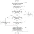
在一种实现方式中,图3示出本申请实施例提供的一种地址映射关系,上0述的步骤203可以包括如下步骤:In one implementation, FIG. 3 shows an address mapping relationship provided by the embodiment of the present application, and the above-mentioned
步骤401:根据预先设置的逻辑地址与物理地址的映射关系,获取与所述待存储数据的目标逻辑地址对应的多个目标物理地址,其中,所述映射关系包括一个逻辑地址与多个物理地址的对应关系;Step 401: Obtain multiple target physical addresses corresponding to the target logical address of the data to be stored according to the preset mapping relationship between logical addresses and physical addresses, wherein the mapping relationship includes one logical address and multiple physical addresses corresponding relationship;
步骤402:将所述待存储数据存储至所述多个目标物理地址。Step 402: Store the data to be stored in the multiple target physical addresses.
5在本申请实施例中,通过一个逻辑地址对应多个物理地址的对应关系,扩5 In the embodiment of this application, through the correspondence between one logical address and multiple physical addresses, the extended
大数据的可用的存储空间,将待存储数据存储到多个目标物理地址,例如逻辑地址L1对应多个物理地址P1及P1’,如图3所示,通过数据存储的冗余来提升数据存储的性能、寿命等可靠性指标。The available storage space for big data stores the data to be stored in multiple target physical addresses. For example, logical address L1 corresponds to multiple physical addresses P1 and P1'. As shown in Figure 3, data storage is improved through data storage redundancy Performance, life and other reliability indicators.
在一种实现方式中,上述的步骤202可以包括以下步骤:In an implementation manner, the
步骤501:确定所述存储器设置的存储模式为高容量模式;Step 501: Determine that the storage mode set by the memory is a high-capacity mode;
步骤502:在所述存储器的UFS的控制器的第一缓存区域存在可用的存储空间的情况下,确定所述目标缓存模块为所述第一缓存区域。Step 502: If there is available storage space in the first cache area of the UFS controller of the memory, determine that the target cache module is the first cache area.
在本申请实施例中,确定存储器的存储模式为高容量模式时,在该存储器的UFS的控制器的第一缓存区域存在可用的存储空间时,确定该第一缓存区域为目标缓存模块,将待存储数据暂时存储在第一缓存区域,不将待存储数据转存于NAND,该NAND依然能够作为具有可用存储空间的存储模块,为数据的存储提供了更大的存储空间,同时提升数据存储的性能。In the embodiment of the present application, when it is determined that the storage mode of the memory is the high-capacity mode, when there is available storage space in the first cache area of the UFS controller of the memory, the first cache area is determined to be the target cache module, and the The data to be stored is temporarily stored in the first cache area, and the data to be stored is not transferred to NAND. The NAND can still be used as a storage module with available storage space, providing a larger storage space for data storage and improving data storage. performance.
在一种实现方式中,在上述步骤502之后还可以包括步骤503:在所述存储器的UFS的控制器的第一缓存区域没有可用的存储空间、且DRAM的第三缓存区域存在可用的存储空间的情况下,确定所述目标缓存模块为所述第三缓存区域。In one implementation, after the above step 502, step 503 may also be included: there is no available storage space in the first cache area of the UFS controller of the memory, and there is available storage space in the third cache area of the DRAM In the case of , determine that the target cache module is the third cache area.
在本申请实施例中,在存储器的存储模式为高容量模式时,存储器的UFS的控制器的第一缓存区域没有可用的存储空间,并且DRAM的第三缓存区域存在可用的存储空间的情况下,将该第三缓存区域确定为目标缓存模块,能够在第三缓存区域进行待存储数据的存储。In the embodiment of the present application, when the storage mode of the memory is the high-capacity mode, the first cache area of the UFS controller of the memory has no available storage space, and the third cache area of the DRAM has available storage space , the third cache area is determined as the target cache module, and the data to be stored can be stored in the third cache area.
在一种实现方式中,在上述步骤503之后还包括步骤504:将所述第一缓存区域存储的数据转存到所述NAND。In an implementation manner, after the above step 503, a step 504 is further included: dumping the data stored in the first cache area to the NAND.
在本申请实施例中,在存储器的存储模式为高容量模式时,在第一缓存区域没有可用的存储空间、且将待存储数据暂时存储在第三缓存区域的同时,将已存储在第一缓存区域的数据转存到存储单元为QLC的NAND的第四缓存区域中,使得第一缓存区域存余可用的存储空间,能够再次作为缓存模块进行存储数据,利用了QLC存储容量大且单位存储成本低的优点,减少对NAND的存取存储操作,提升数据存储的性能及寿命。In the embodiment of the present application, when the storage mode of the memory is the high-capacity mode, when the first cache area has no available storage space and the data to be stored is temporarily stored in the third cache area, the data already stored in the first The data in the cache area is transferred to the fourth cache area of NAND whose storage unit is QLC, so that the available storage space in the first cache area can be used as a cache module to store data again, taking advantage of the large storage capacity of QLC and the unit storage The advantage of low cost reduces the access and storage operations of NAND, and improves the performance and lifespan of data storage.
在一种实现方式中,上述的步骤202可以包括以下步骤:In an implementation manner, the
步骤601:确定所述存储器设置的存储模式为标准模式;Step 601: Determine that the storage mode set by the memory is the standard mode;
步骤602:在所述存储器的UFS的控制器的第一缓存区域存在可用的存储空间的情况下,确定所述目标缓存模块为所述第一缓存区域;在所述存储器的UFS的控制器的第一缓存区域没有可用的存储空间的情况下,将所述第一缓存区域存储的数据转存到所述NAND。Step 602: If there is available storage space in the first cache area of the UFS controller of the memory, determine that the target cache module is the first cache area; in the UFS controller of the memory When the first cache area has no available storage space, dump the data stored in the first cache area to the NAND.
在本申请实施例中,确定存储器的存储模式为标准模式时,在该存储器的UFS的控制器的第一缓存区域存在可用的存储空间的情况下,确定该第一缓存区域为目标缓存模块,将待存储数据暂时存储在第一缓存区域,不将待存储数据转存于NAND;然后在该第一缓存区域没有可用的存储空间的情况下,再将已存储在第一缓存区域的数据转存到存储单元为QLC的NAND的第四缓存区域中,以使第一缓存区域可以再次作为缓存模块进行存储数据。In the embodiment of the present application, when it is determined that the storage mode of the memory is the standard mode, if there is available storage space in the first cache area of the UFS controller of the memory, the first cache area is determined to be the target cache module, Temporarily store the data to be stored in the first cache area without dumping the data to be stored in NAND; and then transfer the data already stored in the first cache area if there is no available storage space in the first cache area Stored in the fourth cache area of NAND whose storage unit is QLC, so that the first cache area can be used as a cache module again to store data.
在一种实施例中,参照图4,该数据存储方法包括如下步骤:In one embodiment, referring to Fig. 4, the data storage method includes the following steps:
步骤410:获取待存储数据,设置存储器的存储模式为高可靠模式;Step 410: Obtain the data to be stored, and set the storage mode of the memory as a high-reliability mode;
步骤420:配置高可靠模式对应的地址映射表;Step 420: Configuring an address mapping table corresponding to the high reliability mode;
步骤430:判断第二缓存区域是否存在可用的存储空间;Step 430: Determine whether there is available storage space in the second cache area;
步骤440:若是,将待存储数据存储到第二缓存区域;Step 440: If yes, store the data to be stored in the second cache area;
步骤450:若否,判断第一缓存区域是否存在可用的存储空间;Step 450: If not, determine whether there is available storage space in the first cache area;
步骤460:若是,将待存储数据存储到第一缓存区域;Step 460: If yes, store the data to be stored in the first cache area;
步骤470:若否,将待存储数据存储到第三缓存区域;Step 470: If not, store the data to be stored in the third cache area;
步骤480:将所述第二缓存区域存储的数据转存到所述NAND的第四缓存区域。Step 480: Transfer the data stored in the second cache area to the fourth cache area of the NAND.
本实施例通过获取待存储数据;根据存储器设置的存储模式,确定所述待存储数据存储的目标缓存模块,其中,所述存储模式包括以下之一:高可靠模式、高容量模式以及标准模式,不同存储模式对应的缓存模块不完全相同;将所述待存储数据存储到所述目标缓存模块;其中,所述存储器包括如第一方面所述的存储器,提供了多种存储模式可供选择,通过设置的不同的存储模式,由于使用的目标存储模块所具有的特点能够提升数据存储的性能、寿命等可靠性指标,也能够满足用户在不同情况下对数据存储的需求。In this embodiment, by obtaining the data to be stored; according to the storage mode set by the memory, the target cache module for storing the data to be stored is determined, wherein the storage mode includes one of the following: high reliability mode, high capacity mode and standard mode, The cache modules corresponding to different storage modes are not exactly the same; the data to be stored is stored in the target cache module; wherein, the memory includes the memory as described in the first aspect, providing a variety of storage modes to choose from, By setting different storage modes, due to the characteristics of the target storage module used, the reliability indicators such as data storage performance and life can be improved, and it can also meet the needs of users for data storage in different situations.
基于相同的技术构思,本申请实施例还提供了一种电子设备,该电子设备用于执行上述的数据存储方法,图6为实现本申请各个实施例的一种电子设备的结构示意图。电子设备可因配置或性能不同而产生比较大的差异,可以包括处理器(processor)610、通信接口(Communications Interface)620、存储器(memory)630和通信总线640,其中,处理器610,通信接口620,存储器630通过通信总线640完成相互间的通信。处理器610可以调用存储在存储器630上并可在处理器610上运行的计算机程序,以执行下述步骤:获取待存储数据;根据存储器设置的存储模式,确定所述待存储数据存储的目标缓存模块,其中,所述存储模式包括以下之一:高可靠模式、高容量模式以及标准模式,不同存储模式对应的缓存模块不完全相同;将所述待存储数据存储到所述目标缓存模块。Based on the same technical concept, an embodiment of the present application also provides an electronic device, which is used to execute the above-mentioned data storage method. FIG. 6 is a schematic structural diagram of an electronic device implementing various embodiments of the present application. Electronic equipment may have relatively large differences due to different configurations or performances, and may include a processor (processor) 610, a communication interface (Communications Interface) 620, a memory (memory) 630, and a
具体执行步骤可以参见上述数据存储方法实施例的各个步骤,且能达到相同的技术效果,为避免重复,这里不再赘述。For specific execution steps, reference may be made to the various steps in the above embodiments of the data storage method, and the same technical effect can be achieved. To avoid repetition, details are not repeated here.
需要说明的是,本申请实施例中的电子设备包括:终端或除终端之外的其他设备。It should be noted that the electronic device in the embodiment of the present application includes: a terminal or other devices except the terminal.
以上电子设备结构并不构成对电子设备的限定,电子设备可以包括比图示更多或更少的部件,或者组合某些部件,或者不同的部件布置,例如,输入单元,可以包括图形处理器(Graphics Processing Unit,GPU)和麦克风,显示单元可以采用液晶显示器、有机发光二极管等形式来配置显示面板。用户输入单元包括触控面板以及其他输入设备中的至少一种。触控面板也称为触摸屏。其他输入设备可以包括但不限于物理键盘、功能键(比如音量控制按键、开关按键等)、轨迹球、鼠标、操作杆,在此不再赘述。The above electronic device structure does not constitute a limitation to the electronic device, and the electronic device may include more or fewer components than shown in the illustration, or combine certain components, or arrange different components, for example, an input unit may include a graphics processor (Graphics Processing Unit, GPU) and a microphone, the display unit can be configured with a display panel in the form of a liquid crystal display, an organic light-emitting diode, or the like. The user input unit includes at least one of a touch panel and other input devices. A touch panel is also called a touch screen. Other input devices may include, but are not limited to, physical keyboards, function keys (such as volume control buttons, switch buttons, etc.), trackballs, mice, and joysticks, which will not be repeated here.
存储器可用于存储软件程序以及各种数据。存储器可主要包括存储程序或指令的第一存储区和存储数据的第二存储区,其中,第一存储区可存储操作系统、至少一个功能所需的应用程序或指令(比如声音播放功能、图像播放功能等)等。此外,存储器可以包括易失性存储器或非易失性存储器,或者,存储器可以包括易失性和非易失性存储器两者。其中,非易失性存储器可以是只读存储器(Read-Only Memory,ROM)、可编程只读存储器(Programmable ROM,PROM)、可擦除可编程只读存储器(Erasable PROM,EPROM)、电可擦除可编程只读存储器(Electrically EPROM,EEPROM)或闪存。易失性存储器可以是随机存取存储器(Random Access Memory,RAM),静态随机存取存储器(Static RAM,SRAM)、DRAM、同步动态随机存取存储器(Synchronous DRAM,SDRAM)、双倍数据速率同步动态随机存取存储器(Double Data Rate SDRAM,DDRSDRAM)、增强型同步动态随机存取存储器(EnhancedSDRAM,ESDRAM)、同步连接动态随机存取存储器(Synch link DRAM,SLDRAM)和直接内存总线随机存取存储器(Direct Rambus RAM,DRRAM)。The memory can be used to store software programs as well as various data. The memory may mainly include a first storage area for storing programs or instructions and a second storage area for storing data, wherein the first storage area may store an operating system, application programs or instructions required by at least one function (such as sound playback function, image playback function, etc.) etc. Also, memory may include volatile memory or nonvolatile memory, or memory may include both volatile and nonvolatile memory. Among them, the non-volatile memory can be read-only memory (Read-Only Memory, ROM), programmable read-only memory (Programmable ROM, PROM), erasable programmable read-only memory (Erasable PROM, EPROM), electronically programmable Erase Programmable Read-Only Memory (Electrically EPROM, EEPROM) or Flash. Volatile memory can be random access memory (Random Access Memory, RAM), static random access memory (Static RAM, SRAM), DRAM, synchronous dynamic random access memory (Synchronous DRAM, SDRAM), double data rate synchronous Dynamic random access memory (Double Data Rate SDRAM, DDRSDRAM), enhanced synchronous dynamic random access memory (EnhancedSDRAM, ESDRAM), synchronous connection dynamic random access memory (Synch link DRAM, SLDRAM) and direct memory bus random access memory (Direct Rambus RAM, DRRAM).
处理器可包括一个或多个处理单元;可选的,处理器集成应用处理器和调制解调处理器,其中,应用处理器主要处理涉及操作系统、用户界面和应用程序等的操作,调制解调处理器主要处理无线通信信号,如基带处理器。可以理解的是,上述调制解调处理器也可以不集成到处理器中。The processor may include one or more processing units; optionally, the processor integrates an application processor and a modem processor, wherein the application processor mainly handles operations related to the operating system, user interface, and application programs, and the modem The tone processor mainly processes wireless communication signals, such as a baseband processor. It can be understood that the foregoing modem processor may not be integrated into the processor.
本申请实施例另提供了一种芯片,所述芯片包括处理器和通信接口,所述通信接口和所述处理器耦合,所述处理器用于运行程序或指令,实现上述数据存储方法实施例的各个过程,且能达到相同的技术效果,为避免重复,这里不再赘述。The embodiment of the present application further provides a chip, the chip includes a processor and a communication interface, the communication interface is coupled to the processor, and the processor is used to run programs or instructions to implement the above data storage method embodiment Each process can achieve the same technical effect, so in order to avoid repetition, it will not be repeated here.
应理解,本申请实施例提到的芯片还可以称为系统级芯片、系统芯片、芯片系统或片上系统芯片等。It should be understood that the chips mentioned in the embodiments of the present application may also be called system-on-chip, system-on-chip, system-on-a-chip, or system-on-a-chip.
需要说明的是,在本文中,术语“包括”、“包含”或者其任何其他变体意在涵盖非排他性的包含,从而使得包括一系列要素的过程、方法、物品或者装置不仅包括那些要素,而且还包括没有明确列出的其他要素,或者是还包括为这种过程、方法、物品或者装置所固有的要素。在没有更多限制的情况下,由语句“包括一个……”限定的要素,并不排除在包括该要素的过程、方法、物品或者装置中还存在另外的相同要素。此外,需要指出的是,本申请实施方式中的方法和装置的范围不限按示出或讨论的顺序来执行功能,还可包括根据所涉及的功能按基本同时的方式或按相反的顺序来执行功能,例如,可以按不同于所描述的次序来执行所描述的方法,并且还可以添加、省去、或组合各种步骤。另外,参照某些示例所描述的特征可在其他示例中被组合。It should be noted that, in this document, the term "comprising", "comprising" or any other variation thereof is intended to cover a non-exclusive inclusion such that a process, method, article or apparatus comprising a set of elements includes not only those elements, It also includes other elements not expressly listed, or elements inherent in the process, method, article, or device. Without further limitations, an element defined by the phrase "comprising a ..." does not preclude the presence of additional identical elements in the process, method, article, or apparatus comprising that element. In addition, it should be pointed out that the scope of the methods and devices in the embodiments of the present application is not limited to performing functions in the order shown or discussed, and may also include performing functions in a substantially simultaneous manner or in reverse order according to the functions involved. Functions are performed, for example, the described methods may be performed in an order different from that described, and various steps may also be added, omitted, or combined. Additionally, features described with reference to certain examples may be combined in other examples.
通过以上的实施方式的描述,本领域的技术人员可以清楚地了解到上述实施例方法可借助软件加必需的通用硬件平台的方式来实现,当然也可以通过硬件,但很多情况下前者是更佳的实施方式。基于这样的理解,本申请的技术方案本质上或者说对现有技术做出贡献的部分可以以软件产品的形式体现出来,该计算机软件产品存储在一个存储介质(如ROM/RAM、磁碟、光盘)中,包括若干指令用以使得一台终端(可以是手机,计算机,服务器,空调器,或者网络设备等)执行本申请各个实施例所述的方法。Through the description of the above embodiments, those skilled in the art can clearly understand that the methods of the above embodiments can be implemented by means of software plus a necessary general-purpose hardware platform, and of course also by hardware, but in many cases the former is better implementation. Based on such an understanding, the technical solution of the present application can be embodied in the form of a software product in essence or the part that contributes to the prior art, and the computer software product is stored in a storage medium (such as ROM/RAM, disk, CD) contains several instructions to enable a terminal (which may be a mobile phone, a computer, a server, an air conditioner, or a network device, etc.) to execute the methods described in various embodiments of the present application.
上面结合附图对本申请的实施例进行了描述,但是本申请并不局限于上述的具体实施方式,上述的具体实施方式仅仅是示意性的,而不是限制性的,本领域的普通技术人员在本申请的启示下,在不脱离本申请宗旨和权利要求所保护的范围情况下,还可做出很多形式,均属于本申请的保护之内。The embodiments of the present application have been described above in conjunction with the accompanying drawings, but the present application is not limited to the above-mentioned specific implementations. The above-mentioned specific implementations are only illustrative and not restrictive. Those of ordinary skill in the art will Under the inspiration of this application, without departing from the purpose of this application and the scope of protection of the claims, many forms can also be made, all of which belong to the protection of this application.
Claims (12)
Priority Applications (1)
| Application Number | Priority Date | Filing Date | Title |
|---|---|---|---|
| CN202211731504.1ACN115981565A (en) | 2022-12-30 | 2022-12-30 | Memory, data storage method and electronic device |
Applications Claiming Priority (1)
| Application Number | Priority Date | Filing Date | Title |
|---|---|---|---|
| CN202211731504.1ACN115981565A (en) | 2022-12-30 | 2022-12-30 | Memory, data storage method and electronic device |
Publications (1)
| Publication Number | Publication Date |
|---|---|
| CN115981565Atrue CN115981565A (en) | 2023-04-18 |
Family
ID=85957684
Family Applications (1)
| Application Number | Title | Priority Date | Filing Date |
|---|---|---|---|
| CN202211731504.1APendingCN115981565A (en) | 2022-12-30 | 2022-12-30 | Memory, data storage method and electronic device |
Country Status (1)
| Country | Link |
|---|---|
| CN (1) | CN115981565A (en) |
Cited By (1)
| Publication number | Priority date | Publication date | Assignee | Title |
|---|---|---|---|---|
| CN118354140A (en)* | 2024-03-29 | 2024-07-16 | 重庆赛力斯凤凰智创科技有限公司 | Video stream storage method, electronic device and storage medium |
- 2022
- 2022-12-30CNCN202211731504.1Apatent/CN115981565A/enactivePending
Cited By (1)
| Publication number | Priority date | Publication date | Assignee | Title |
|---|---|---|---|---|
| CN118354140A (en)* | 2024-03-29 | 2024-07-16 | 重庆赛力斯凤凰智创科技有限公司 | Video stream storage method, electronic device and storage medium |
Similar Documents
| Publication | Publication Date | Title |
|---|---|---|
| US12038834B2 (en) | Memory system and method for controlling nonvolatile memory during command processing without replacing defective blocks | |
| US20240370366A1 (en) | Computing system and method for controlling storage device | |
| EP4109230B1 (en) | Storage system, file storage and reading method, and terminal device | |
| CN103164346B (en) | Use the method and system of LBA bitmap | |
| US7882301B2 (en) | Wear leveling in storage devices based on flash memories and related circuit, system, and method | |
| US7991942B2 (en) | Memory block compaction method, circuit, and system in storage devices based on flash memories | |
| US20080282024A1 (en) | Management of erase operations in storage devices based on flash memories | |
| CN110908927A (en) | Data storage device and method for deleting name space thereof | |
| US7536500B2 (en) | Header blocks for flash memory writes | |
| CN107590080B (en) | Mapping table updating method, memory control circuit unit and memory storage device | |
| US20200320012A1 (en) | Memory system and method for operating the same | |
| US20060004951A1 (en) | Method and apparatus to alter code in a memory | |
| CN117707639B (en) | Application start acceleration method, electronic device and storage medium | |
| CN110879793B (en) | Memory management method, memory storage device and memory control circuit unit | |
| CN116954511A (en) | Storage processing method, electronic device, and readable storage medium | |
| CN113885808A (en) | Mapping information recording method, memory control circuit unit and memory device | |
| CN113885692A (en) | Memory efficiency optimization method, memory control circuit unit and memory device | |
| CN107943710B (en) | Memory management method and memory controller using the same | |
| CN110390985B (en) | Memory management method, memory storage device, and memory control circuit unit | |
| CN116383164A (en) | Data processing method and device | |
| CN115981565A (en) | Memory, data storage method and electronic device | |
| CN106775479B (en) | Memory management method, memory storage device and memory control circuit unit | |
| KR100456736B1 (en) | Method for reducing booting time of a digital device having a flash memory | |
| US20050144389A1 (en) | Method, system, and apparatus for explicit control over a disk cache memory | |
| US11188265B2 (en) | Method for performing storage space management, associated data storage device, and controller thereof |
Legal Events
| Date | Code | Title | Description |
|---|---|---|---|
| PB01 | Publication | ||
| PB01 | Publication | ||
| SE01 | Entry into force of request for substantive examination | ||
| SE01 | Entry into force of request for substantive examination |