CN115976614A - Electroplating apparatus and electroplating method - Google Patents
Electroplating apparatus and electroplating methodDownload PDFInfo
- Publication number
- CN115976614A CN115976614ACN202210164120.XACN202210164120ACN115976614ACN 115976614 ACN115976614 ACN 115976614ACN 202210164120 ACN202210164120 ACN 202210164120ACN 115976614 ACN115976614 ACN 115976614A
- Authority
- CN
- China
- Prior art keywords
- electroplating
- cathode
- metal
- metal sheets
- anode
- Prior art date
- Legal status (The legal status is an assumption and is not a legal conclusion. Google has not performed a legal analysis and makes no representation as to the accuracy of the status listed.)
- Withdrawn
Links
Images


Landscapes
- Electroplating Methods And Accessories (AREA)
Abstract
Translated fromChinese
Description
Translated fromChinese技术领域technical field
本发明涉及一种设备与方法,尤其涉及一种电镀设备与电镀方法。The invention relates to a device and a method, in particular to an electroplating device and an electroplating method.
背景技术Background technique
电镀已广泛地运用于各种领域中,除了传统上作为表面处理的方法外,亦应用于制作电路板、半导体晶片、LED导电基板、及半导体封装等方面,而电镀常具有金属镀层的电镀厚度均匀性的问题。Electroplating has been widely used in various fields. In addition to being traditionally used as a surface treatment method, it is also used in the production of circuit boards, semiconductor chips, LED conductive substrates, and semiconductor packaging. Electroplating often has the thickness of metal plating The question of uniformity.
举例而言,如在电路板的制作过程中,阳极与阴极之间的电力线在靠近待镀基板时常会受到其上膜层特性(例如是绝缘特性或其他会影响电力分布的特性)的影响而转向,产生电力线密度分布不均的情况,如此一来,形成于待镀基板上的金属镀层便会具有电镀厚度均匀性不佳的问题。For example, in the process of making a circuit board, the electric force line between the anode and the cathode is often affected by the properties of the upper film (such as insulation properties or other properties that affect power distribution) when it is close to the substrate to be plated. Turning to produce uneven distribution of electric power line density, so that the metal plating layer formed on the substrate to be plated will have the problem of poor uniformity of plating thickness.
发明内容Contents of the invention
本发明提供一种电镀设备与电镀方法,其可以改善待镀基板上的金属镀层的电镀厚度均匀性不佳的问题。The invention provides an electroplating device and an electroplating method, which can improve the problem of poor uniformity of electroplating thickness of a metal coating on a substrate to be plated.
本发明的一种电镀设备,包括电镀槽、阳极与阴极、电源供应器以及调控板。电镀槽容置有电解液。阳极与阴极皆设置于电镀槽内。电源供应器电性连接至阳极与阴极。调控板设置于阳极与阴极之间。调控板包括多个网孔与多个金属片,且至少一部分金属片与阴极电性连接。An electroplating device of the present invention includes an electroplating tank, an anode and a cathode, a power supply and a control board. The electroplating tank accommodates an electrolytic solution. Both the anode and the cathode are arranged in the electroplating tank. The power supply is electrically connected to the anode and the cathode. The control board is arranged between the anode and the cathode. The regulating plate includes a plurality of mesh holes and a plurality of metal sheets, and at least a part of the metal sheets are electrically connected with the cathode.
在本发明的一实施例中,上述的多个网孔为绝缘网格板的一部分,多个金属片设置于绝缘网格板上,且多个金属片皆与所述阴极电性连接。In an embodiment of the present invention, the above-mentioned plurality of mesh holes is a part of the insulating grid plate, the plurality of metal sheets are disposed on the insulating grid plate, and the plurality of metal sheets are electrically connected to the cathode.
在本发明的一实施例中,仅上述的多个网孔形成通道。In an embodiment of the present invention, only the above-mentioned plurality of meshes form channels.
在本发明的一实施例中,上述的电镀设备还包括以一对一方式连接多个金属片的多条导线。In an embodiment of the present invention, the above-mentioned electroplating equipment further includes a plurality of wires connecting the plurality of metal sheets in a one-to-one manner.
在本发明的一实施例中,上述的电镀设备还包括连接多条导线的控制器,其中多条导线的电流通过控制器汇流至阴极。In an embodiment of the present invention, the above-mentioned electroplating equipment further includes a controller connected to multiple wires, wherein the currents of the multiple wires are converged to the cathode through the controller.
在本发明的一实施例中,上述的多个网孔与多个金属片的形状互补。In an embodiment of the present invention, the shapes of the above-mentioned plurality of mesh holes and the plurality of metal sheets are complementary.
在本发明的一实施例中,上述的多个网孔为绝缘网格板的一部分,多个金属片阵列排列于绝缘网格板上,一部分金属片电性连接至阴极,而另一部分金属片没有电性连接至阴极。In an embodiment of the present invention, the above-mentioned plurality of mesh holes is a part of an insulating grid plate, and a plurality of metal sheets are arranged in an array on the insulating grid plate, a part of the metal sheets are electrically connected to the cathode, and the other part of the metal sheets Not electrically connected to the cathode.
在本发明的一实施例中,每一上述的金属片包括至少一孔洞,且至少一孔洞与多个网孔形成通道。In an embodiment of the present invention, each of the aforementioned metal sheets includes at least one hole, and at least one hole forms a channel with a plurality of mesh holes.
在本发明的一实施例中,上述的电镀设备还包括以一对一方式连接多个金属片的多条导线。In an embodiment of the present invention, the above-mentioned electroplating equipment further includes a plurality of wires connecting the plurality of metal sheets in a one-to-one manner.
在本发明的一实施例中,上述的电镀设备还包括连接所述多条导线的控制器,其中控制器被配置于控制调控板的电性连接状态。In an embodiment of the present invention, the above-mentioned electroplating equipment further includes a controller connected to the plurality of wires, wherein the controller is configured to control the electrical connection state of the regulation board.
本发明的一种电镀方法,至少包括以下步骤。提供电镀设备,其中电镀设备包括电镀槽、阳极与阴极、电源供应器以及调控板。电镀槽容置有电解液。阳极与阴极皆设置于电镀槽内。电源供应器电性连接至阳极与阴极。调控板设置于阳极与阴极之间。调控板包括多个网孔与多个金属片,且至少一部分金属片与阴极电性连接。将待镀基板固定于阴极上。电源供应器供电后于阳极与阴极之间形成多条电力线,多条电力线由阳极朝向阴极移动。多条电力线的一部分驱使电解液中的多个金属离子的一部分通过调控板于待镀基板上形成第一金属镀层。多条电力线的另一部分驱使电解液中的多个金属离子的另一部分于调控板上形成第二金属镀层。An electroplating method of the present invention at least includes the following steps. Electroplating equipment is provided, wherein the electroplating equipment includes an electroplating tank, an anode and a cathode, a power supply and a control board. The electroplating tank accommodates an electrolytic solution. Both the anode and the cathode are arranged in the electroplating tank. The power supply is electrically connected to the anode and the cathode. The control board is arranged between the anode and the cathode. The regulating plate includes a plurality of mesh holes and a plurality of metal sheets, and at least a part of the metal sheets are electrically connected with the cathode. Fix the substrate to be plated on the cathode. After the power supply supplies power, multiple power lines are formed between the anode and the cathode, and the multiple power lines move from the anode to the cathode. A part of the plurality of electric lines drives a part of the plurality of metal ions in the electrolyte to pass through the control plate to form a first metal plating layer on the substrate to be plated. Another part of the plurality of electric lines drives another part of the plurality of metal ions in the electrolyte to form a second metal plating layer on the control plate.
在本发明的一实施例中,上述的多个网孔为绝缘网格板的一部分,所述多个金属片设置于所述绝缘网格板上,且所述多个金属片皆与所述阴极电性连接,以使所述多个金属片上皆具有第二金属镀层。In an embodiment of the present invention, the above-mentioned plurality of mesh holes is a part of an insulating grid plate, the plurality of metal sheets are arranged on the insulating grid plate, and the plurality of metal sheets are all connected to the insulating grid plate. The cathode is electrically connected so that the plurality of metal sheets have the second metal plating layer.
在本发明的一实施例中,上述的多个网孔与多个金属片的形状互补。In an embodiment of the present invention, the shapes of the above-mentioned plurality of mesh holes and the plurality of metal sheets are complementary.
在本发明的一实施例中,上述的电镀设备还包括以一对一方式连接所述多个金属片的多条导线。In an embodiment of the present invention, the above-mentioned electroplating equipment further includes a plurality of wires connecting the plurality of metal sheets in a one-to-one manner.
在本发明的一实施例中,上述的电镀设备还包括连接多条导线的控制器,其中多条导线的电流通过控制器汇流至阴极。In an embodiment of the present invention, the above-mentioned electroplating equipment further includes a controller connected to multiple wires, wherein the currents of the multiple wires are converged to the cathode through the controller.
在本发明的一实施例中,上述的待镀基板包括具有多个开口的干膜,且多个网孔对位于多个开口。In an embodiment of the present invention, the above-mentioned substrate to be plated includes a dry film having a plurality of openings, and a plurality of mesh holes are aligned with the plurality of openings.
在本发明的一实施例中,上述的多个网孔为绝缘网格板的一部分,多个金属片阵列排列于绝缘网格板上,且仅一部分金属片电性连接至阴极,以使仅有一部分金属片上形成有第二金属镀层。In an embodiment of the present invention, the plurality of mesh holes described above are part of an insulating grid plate, and a plurality of metal sheets are arrayed on the insulating grid plate, and only a part of the metal sheets are electrically connected to the cathode, so that only A second metal plating layer is formed on a part of the metal sheets.
在本发明的一实施例中,上述的每一金属片包括至少一孔洞,且不具有第二金属镀层的金属片的孔洞与多个网孔形成通道。In an embodiment of the present invention, each of the aforementioned metal sheets includes at least one hole, and the holes of the metal sheet without the second metal plating layer and the plurality of mesh holes form channels.
在本发明的一实施例中,上述的电镀设备还包括以一对一方式连接所述多个金属片的多条导线。In an embodiment of the present invention, the above-mentioned electroplating equipment further includes a plurality of wires connecting the plurality of metal sheets in a one-to-one manner.
在本发明的一实施例中,上述的电镀设备还包括连接所述多条导线的控制器,其中控制器被配置于控制调控板的电性连接状态。In an embodiment of the present invention, the above-mentioned electroplating equipment further includes a controller connected to the plurality of wires, wherein the controller is configured to control the electrical connection state of the regulation board.
基于上述,本发明的电镀设备在阳极与阴极之间具有调控板的设计,因此多条由阳极朝向阴极移动的电力线的一部分可以驱使电解液中的部分金属离子通过调控板的网孔于待镀基板上形成金属镀层,且前述多条电力线的另一部分可以驱使电解液中另一部分金属离子于调控板上的金属片上亦形成金属镀层,如此一来,可以重新分配电力线的分布,使待镀基板上欲形成线路的部分拥有一致的电力线密度,进而可以改善待镀基板上的金属镀层的电镀厚度均匀性不佳的问题。Based on the above, the electroplating equipment of the present invention has the design of the control plate between the anode and the cathode, so a part of the electric force lines moving from the anode to the cathode can drive some metal ions in the electrolyte to pass through the mesh of the control plate to be plated. A metal coating is formed on the substrate, and another part of the aforementioned plurality of power lines can drive another part of the metal ions in the electrolyte to form a metal coating on the metal sheet on the control board. In this way, the distribution of the power lines can be redistributed, so that the substrate to be plated The part on which the circuit is to be formed has a consistent electric force line density, which can improve the problem of poor uniformity of the electroplating thickness of the metal plating layer on the substrate to be plated.
为让本发明的上述特征和优点能更明显易懂,下文特举实施例,并配合附图作详细说明如下。In order to make the above-mentioned features and advantages of the present invention more comprehensible, the following specific embodiments are described in detail with reference to the accompanying drawings.
附图说明Description of drawings
图1A是依据本发明一实施例的电镀方法的流程图;1A is a flow chart of an electroplating method according to an embodiment of the present invention;
图1B是本发明一实施例的电镀设备的侧视示意图;Figure 1B is a schematic side view of an electroplating device according to an embodiment of the present invention;
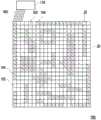
图1C是本发明一实施例的电镀设备的调控板的俯视示意图;Fig. 1C is a schematic top view of a control panel of an electroplating device according to an embodiment of the present invention;
图1D是本发明另一实施例的调控板的俯视示意图。FIG. 1D is a schematic top view of a control plate according to another embodiment of the present invention.
具体实施方式Detailed ways
现将详细地参考本发明的示范性实施例,示范性实施例的实例说明于附图中。只要有可能,相同元件符号在附图和描述中用来表示相同或相似部分。Reference will now be made in detail to the exemplary embodiments of the present invention, examples of which are illustrated in the accompanying drawings. Wherever possible, the same reference numbers will be used in the drawings and description to refer to the same or like parts.
以下将参考附图来全面地描述本发明的例示性实施例,但本发明还可按照多种不同形式来实施,且不应解释为限于本文所述的实施例。在附图中,为了清楚起见,各区域、部位及层的大小与厚度可不按实际比例绘制。为了方便理解,下述说明中相同的元件将以相同的符号标示来说明。Exemplary embodiments of the present invention will be fully described below with reference to the accompanying drawings, but the invention may also be embodied in many different forms and should not be construed as being limited to the embodiments described herein. In the drawings, for the sake of clarity, the sizes and thicknesses of regions, parts and layers may not be drawn in actual scale. In order to facilitate understanding, the same elements in the following description will be described with the same symbols.
参照本实施例的附图以更全面地阐述本发明。然而,本发明亦可以各种不同的形式体现,而不应限于本文中所述的实施例。附图中的层或区域的厚度、尺寸或大小会为了清楚起见而放大。相同或相似的参考号码表示相同或相似的元件,以下段落将不再一一赘述。The present invention will be described more fully with reference to the accompanying drawings of this embodiment. However, the present invention can also be embodied in various forms and should not be limited to the embodiments described herein. The thickness, size or size of layers or regions in the drawings may be exaggerated for clarity. The same or similar reference numerals denote the same or similar elements, and the following paragraphs will not repeat them one by one.
本文所使用的方向用语(例如,上、下、右、左、前、后、顶部、底部)仅作为参看所绘附图使用且不意欲暗示绝对定向。Directional terms (eg, up, down, right, left, front, back, top, bottom) as used herein are used only as a reference to a drawn figure and are not intended to imply absolute orientation.
应当理解,尽管术语”第一”、”第二”、”第三”等在本文中可以用于描述各种元件、部件、区域、层和/或部分,但是这些元件、部件、区域、和/或部分不应受这些术语的限制。这些术语仅用于将一个元件、部件、区域、层或部分与另一个元件、部件、区域、层或部分区分开。It should be understood that although the terms "first", "second", "third" etc. may be used herein to describe various elements, components, regions, layers and/or sections, these elements, components, regions, and and/or parts should not be limited by these terms. These terms are only used to distinguish one element, component, region, layer or section from another element, component, region, layer or section.
除非另有定义,本文使用的所有术语(包括技术和科学术语)具有与本发明所属领域的普通技术人员通常理解的相同的含义。Unless otherwise defined, all terms (including technical and scientific terms) used herein have the same meaning as commonly understood by one of ordinary skill in the art to which this invention belongs.
图1A是依据本发明一实施例的电镀方法的流程图。图1B是本发明一实施例的电镀设备的侧视示意图。图1C是本发明一实施例的电镀设备的调控板的俯视示意图。图1D是本发明另一实施例的调控板的俯视示意图。FIG. 1A is a flowchart of an electroplating method according to an embodiment of the invention. FIG. 1B is a schematic side view of an electroplating device according to an embodiment of the present invention. FIG. 1C is a schematic top view of a control panel of an electroplating device according to an embodiment of the present invention. FIG. 1D is a schematic top view of a control plate according to another embodiment of the present invention.
请参考图1A、图1B与图1C,以下通过使用附图说明本发明一实施例的电镀方法的主要流程。首先,提供电镀设备100,其中电镀设备100包括电镀槽110、阳极120与阴极130、电源供应器140以及调控板150(步骤S100)。进一步而言,电镀槽110容置有电解液112,阳极120与阴极130皆设置于电镀槽110内,且电源供应器140电性连接至阳极120与阴极130,且调控板150设置于阳极120与阴极130之间(图1B中示意地示出阴极130与两个阳极120之间分别夹有一片调控板150),其中调控板150包括多个网孔152与多个金属片154,且至少一部分金属片154与阴极130电性连接。在此,电解槽110、电解液112、阳极120、阴极130的材料与种类可以依照实际待镀金属(如镀铜)的种类而调整,本发明不加以限制。此外,与阴极130电性连接的金属片154可以具有与阴极130相同的还原金属机制。应说明的是,电镀设备100的其他具体细节会于下方进一步说明。Please refer to FIG. 1A , FIG. 1B and FIG. 1C , and the main flow of the electroplating method according to an embodiment of the present invention will be described below by using the drawings. Firstly, an
接着,将待镀基板S固定于阴极130上(步骤S200)。然后,电源供应器140供电后于阳极120与阴极130之间形成多条电力线L(可以是阳极120通电后游离出的电子移动方向),多条电力线L由阳极120朝向阴极130移动(步骤S300)。接着,多条电力线L的一部分(如图1B中的电力线L1)驱使电解液112中的多个金属离子Y的一部分通过调控板150于待镀基板S上形成第一金属镀层10(步骤S400)。此外,多条电力线L的另一部分(如图1B中的L2)驱使电解液112中的多个金属离子Y的另一部分于调控板150上形成第二金属镀层20(步骤S500)。在此,多条电力线L可以是平行且均匀地由阳极120发出,且电力线L亦是平行且均匀地抵达待镀基板S上。Next, the substrate S to be plated is fixed on the cathode 130 (step S200 ). Then, after the
据此,本实施例的电镀设备100在阳极120与阴极130之间具有调控板150的设计,因此多条由阳极120朝向阴极130移动的电力线L的一部分(电力线L1)可以驱使电解液112中的部分金属离子Y通过调控板150的网孔152于待镀基板S上形成金属镀层(第一金属镀层10),且多条电力线L的另一部分(电力线L2)可以驱使电解液112中另一部分金属离子Y于调控板150的金属片154上亦形成金属镀层(第二金属镀层20),如此一来,可以重新分配电力线L的分布,使待镀基板S上欲形成线路的部分拥有一致的电力线密度,进而可以改善待镀基板S上的金属镀层(第一金属镀层10)的电镀厚度均匀性不佳的问题。Accordingly, the
在一些实施例中,金属离子Y可以为铜离子(Cu2+),因此待镀基板S上的第一金属镀层10与调控板150上的第二金属镀层20可以为还原铜,但本发明不限于此。In some embodiments, the metal ion Y can be copper ion (Cu2+), so the
在本实施例中,网孔152为绝缘网格板30的一部分,多个金属片154设置于绝缘网格板30上,且多个金属片154皆与阴极130电性连接,以使多个金属片154上皆具有第二金属镀层20。进一步而言,本实施例的调控板150的制造方法例如包括以下步骤。首先,提供与待镀基板S的尺寸实质上相同的绝缘网格板30,其中绝缘网格板30包括格线32与格线32所界定出的网孔152。接着,将金属板(例如是全铜板)黏贴在绝缘网格板30上。然后,以蚀刻的方式形成所需的图案,接着镀一层镍金或镍钯金或其他金属保护层(未示出),该保护层不会被蚀刻液所攻击,当作是后面要剥除镀铜时的阻绝层(Stop Barrier),(如图1C中多个金属片154所形成的图案)。或是金属板直接采用不会被蚀刻液所攻击的金属(例如是不锈钢),先制作完图案后,再黏贴在绝缘网格板30上,则可以不需要金属保护层。In this embodiment, the
进一步而言,待镀基板S可以包括具有多个开口42的干膜40,将对应于干膜40的开口42的位置的金属蚀刻掉(多个网孔152可以对位于多个开口42),以使电力线L通过,而将对应于干膜40的覆盖部分44的位置的金属保留,使其与阴极130电性连接,以使电力线L可以驱使金属离子Y上镀,进而使电力线L终止于该些金属片154上,因此多个网孔152与多个金属片154的形状可以是互补,但本发明不限于此。在此,干膜40的材料例如是绝缘材料。Further, the substrate S to be plated may include a
应说明的是,本发明不限制于上述调控板150的态样,请参考图1C与图1D,调控板亦可以替换成另一实施例的调控板150A,其中调控板150A与调控板150差异在于:多个金属片154A阵列排列于绝缘网格板30上,一部分金属片154A电性连接至阴极130,而另一部分金属片154A没有电性连接至阴极130,换句话说,仅一部分金属片154A电性连接至阴极130,以使仅有一部分金属片154A上形成有第二金属镀层20。It should be noted that the present invention is not limited to the aspect of the
进一步而言,在图1C的实施例中,仅多个网孔152可以形成通道,以使电力线L与金属离子Y通过,换句话说,电力线L与金属离子Y并不会通过金属片154,而在图1D的实施例中,每一金属片154A包括至少一孔洞H,且其上未形成第二金属镀层20的金属片154A(没有电性连接至阴极130的金属片154A)的孔洞H可以与多个网孔152形成通道(其他网孔152的部分或全部亦可以单独形成通道)。在此,尽管图1D的孔洞H示出为圆形,但本发明不限制孔洞H形状,例如可以是矩形或多边形,而每一金属片154A的孔洞H数量也不限制为一个,孔洞H数量可以依照实际设计需求而定。此外,在图1D的实施例中,金属片154A例如是钢片或其他较不会被蚀刻的金属,且可以是一个金属片154A对应多个网孔152的方式设置,但本发明不限于此。Further, in the embodiment of FIG. 1C, only a plurality of mesh holes 152 can form a channel, so that the electric force line L and the metal ion Y can pass through, in other words, the electric force line L and the metal ion Y will not pass through the
在一些实施例中,电镀设备100还包括多条导线160,其中多条导线160以一对一方式连接多个金属片154/金属片154A。应说明的是,图1C与图1D中仅示意的示出具有多条导线160以用于说明,而未实际示出出导线160与金属片154/金属片154A的连接细节。In some embodiments, the
此外,在图1C的实施例中,电镀设备100还包括控制器170,其中控制器170连接前述多条导线160,以使多条导线160的电流可以通过控制器170汇流至阴极130,而在图1D的实施例中,控制器170可以进一步用以控制多条导线160的电性连接状态,举例而言,控制器170可以仅使一部分的导线160导通(金属片154A电性连接至阴极130),以使仅有一部分金属片154A上形成有第二金属镀层20,换句话说,控制器170可以使另一部分的导线160不导通(金属片154A没有电性连接至阴极130),因此另一部分金属片154A上不会形成有第二金属镀层20,且电力线L可以通过金属片154A上的孔洞H,但本发明不限于此。In addition, in the embodiment of FIG. 1C, the
在一些实施例中,待镀基板S上的欲形成线路的部分可以包括线路密集区与线路空旷区(未示出),而在线路密集区的金属镀层的电镀厚度均匀性不佳的问题会更加明显,因此本实施例的电镀设备100可以更显著地改善待镀基板S的线路密集区的金属镀层的电镀厚度均匀性不佳的问题,但本发明不限于此,在线路空旷区亦可以具有改善效果。In some embodiments, the portion of the circuit to be formed on the substrate S to be plated may include a circuit dense area and a circuit empty area (not shown), and the problem of poor uniformity of the plating thickness of the metal plating layer in the circuit dense area will cause It is more obvious, so the
在一些实施例中,待镀基板S可以还包括晶种层(seed layer)50,因此第一金属镀层10可以是上镀于晶种层50上,但本发明不限于此。In some embodiments, the substrate S to be plated may further include a
在一些实施例中,网孔152的形状也可以依照实际设计需求而定,本发明不加以限制。In some embodiments, the shape of the
在一些实施例中,调控板150与待镀基板S之间的距离可以介于2毫米(mm)至5厘米(cm)之间,但本发明不限于此。In some embodiments, the distance between the regulating
在一些实施例中,电镀设备100还包括夹头180与喷嘴(未示出),其中夹头180被配置于夹持待镀基板S,而喷嘴被配置于改善金属离子质量传送的问题,但本发明不限于此。In some embodiments, the
在一些实施例中,调控板上所形成的金属镀层可以于电镀完成后使用蚀刻液进行剥除,以使调控板可以重复利用,降低整体电镀成本,但本发明不限于此。In some embodiments, the metal plating formed on the control plate can be stripped with an etching solution after the electroplating is completed, so that the control plate can be reused and the overall electroplating cost is reduced, but the invention is not limited thereto.
综上所述,本发明的电镀设备在阳极与阴极之间具有调控板的设计,因此多条由阳极朝向阴极移动的电力线的一部分可以驱使电解液中的部分金属离子通过调控板的网孔于待镀基板上形成金属镀层,且前述多条电力线的另一部分可以驱使电解液中另一部分金属离子于调控板上的金属片上亦形成金属镀层,如此一来,可以重新分配电力线的分布,使待镀基板上欲形成线路的部分拥有一致的电力线密度,进而可以改善待镀基板上的电镀厚度均匀性不佳的问题。In summary, the electroplating equipment of the present invention has a control plate design between the anode and the cathode, so a part of the electric force lines moving from the anode to the cathode can drive part of the metal ions in the electrolyte to pass through the mesh of the control plate to A metal coating is formed on the substrate to be plated, and another part of the aforementioned plurality of power lines can drive another part of the metal ions in the electrolyte to form a metal coating on the metal sheet on the control board. In this way, the distribution of the power lines can be redistributed, so that The portion of the plated substrate to be formed with a circuit has a consistent electric force line density, which can improve the problem of poor uniformity of the plating thickness on the plated substrate.
最后应说明的是:以上各实施例仅用以说明本发明的技术方案,而非对其限制;尽管参照前述各实施例对本发明进行了详细的说明,本领域的普通技术人员应当理解:其依然可以对前述各实施例所记载的技术方案进行修改,或者对其中部分或者全部技术特征进行等同替换;而这些修改或者替换,并不使相应技术方案的本质脱离本发明各实施例技术方案的范围。Finally, it should be noted that: the above embodiments are only used to illustrate the technical solutions of the present invention, rather than limiting them; although the present invention has been described in detail with reference to the foregoing embodiments, those of ordinary skill in the art should understand that: It is still possible to modify the technical solutions described in the foregoing embodiments, or perform equivalent replacements for some or all of the technical features; and these modifications or replacements do not make the essence of the corresponding technical solutions deviate from the technical solutions of the various embodiments of the present invention. scope.
Claims (20)
Translated fromChineseApplications Claiming Priority (2)
| Application Number | Priority Date | Filing Date | Title |
|---|---|---|---|
| US202163255438P | 2021-10-14 | 2021-10-14 | |
| US63/255,438 | 2021-10-14 |
Publications (1)
| Publication Number | Publication Date |
|---|---|
| CN115976614Atrue CN115976614A (en) | 2023-04-18 |
Family
ID=85961140
Family Applications (3)
| Application Number | Title | Priority Date | Filing Date |
|---|---|---|---|
| CN202210164120.XAWithdrawnCN115976614A (en) | 2021-10-14 | 2022-02-22 | Electroplating apparatus and electroplating method |
| CN202210259976.5AActiveCN115976607B (en) | 2021-10-14 | 2022-03-16 | Electroplating equipment and electroplating method |
| CN202210354578.1AActiveCN115976608B (en) | 2021-10-14 | 2022-04-06 | Electroplating equipment and electroplating method |
Family Applications After (2)
| Application Number | Title | Priority Date | Filing Date |
|---|---|---|---|
| CN202210259976.5AActiveCN115976607B (en) | 2021-10-14 | 2022-03-16 | Electroplating equipment and electroplating method |
| CN202210354578.1AActiveCN115976608B (en) | 2021-10-14 | 2022-04-06 | Electroplating equipment and electroplating method |
Country Status (2)
| Country | Link |
|---|---|
| CN (3) | CN115976614A (en) |
| TW (3) | TWI801144B (en) |
Citations (7)
| Publication number | Priority date | Publication date | Assignee | Title |
|---|---|---|---|---|
| JP2001335991A (en)* | 2000-05-24 | 2001-12-07 | Internatl Business Mach Corp <Ibm> | Metal plating apparatus |
| CN101265606A (en)* | 2007-03-15 | 2008-09-17 | 台湾积体电路制造股份有限公司 | Chemical plating deposition device and method for forming conducting layer structure |
| TW200839038A (en)* | 2007-03-26 | 2008-10-01 | Semi Photonics Co Ltd | Device and method with improved plating film thickness uniformity |
| US20090068771A1 (en)* | 2007-09-10 | 2009-03-12 | Moosung Chae | Electro Chemical Deposition Systems and Methods of Manufacturing Using the Same |
| US20090288954A1 (en)* | 2006-07-14 | 2009-11-26 | Bart Juul Wilhelmina Van Den Bossche | Device suitable for electrochemically processing an object as well as a method for manufacturing such a device, a method for electrochemically processing an object, using such a device, as well as an object formed by using such a method |
| US20110210005A1 (en)* | 2008-09-19 | 2011-09-01 | Elsyca N.V. | Device suitable for the electrochemical processing of an object and a method therefor |
| CN107761158A (en)* | 2017-10-31 | 2018-03-06 | 广东骏亚电子科技股份有限公司 | A kind of electroplating device and electro-plating method |
Family Cites Families (16)
| Publication number | Priority date | Publication date | Assignee | Title |
|---|---|---|---|---|
| US6632335B2 (en)* | 1999-12-24 | 2003-10-14 | Ebara Corporation | Plating apparatus |
| US6802946B2 (en)* | 2000-12-21 | 2004-10-12 | Nutool Inc. | Apparatus for controlling thickness uniformity of electroplated and electroetched layers |
| DE10229001B4 (en)* | 2002-06-28 | 2007-02-15 | Advanced Micro Devices, Inc., Sunnyvale | Method and system for controlling ion distribution during electrodeposition of a metal onto a workpiece surface |
| JP2005023389A (en)* | 2003-07-04 | 2005-01-27 | Seiko Epson Corp | Electroplating method and electroplating apparatus |
| CN1831204A (en)* | 2005-03-08 | 2006-09-13 | 上海艾比西材料科技有限公司 | Method and equipment for electroplating superthick and multiple-hole metals |
| CN101275267B (en)* | 2007-03-26 | 2011-05-25 | 旭明光电股份有限公司 | Electroplating apparatus and electroplating method for improving thickness uniformity |
| JP2010242137A (en)* | 2009-04-02 | 2010-10-28 | Panasonic Corp | Plating equipment |
| CN102534733B (en)* | 2010-12-24 | 2016-01-06 | 北大方正集团有限公司 | Electroplanting device and electro-plating method |
| CN203080091U (en)* | 2013-02-26 | 2013-07-24 | 青岛理工大学 | Electroforming machine with intelligently-controlled electroforming layer thickness |
| US10526719B2 (en)* | 2013-08-21 | 2020-01-07 | Taiwan Semiconductor Manufacturing Company Limited | Magnetic structure for metal plating control |
| CN104862767B (en)* | 2015-05-29 | 2017-05-10 | 东莞市开美电路板设备有限公司 | Copper plating bath |
| JP6004461B2 (en)* | 2016-01-13 | 2016-10-05 | エヌイーシー ショット コンポーネンツ株式会社 | Electroplating method and plating apparatus |
| KR101818182B1 (en)* | 2017-06-23 | 2018-02-21 | (주)에스비메탈 | Apparatus for partially plating mold precisely and method for plating mold using this |
| CN207418883U (en)* | 2017-11-20 | 2018-05-29 | 宁波鑫霖磁业有限公司 | A kind of magnetic material processing electroplanting device |
| JP7256708B2 (en)* | 2019-07-09 | 2023-04-12 | 株式会社荏原製作所 | Plating equipment |
| CN113493920B (en)* | 2020-03-19 | 2022-12-23 | 芯恩(青岛)集成电路有限公司 | Device and method for improving uniformity of electroplating film |
- 2022
- 2022-02-22CNCN202210164120.XApatent/CN115976614A/ennot_activeWithdrawn
- 2022-02-22TWTW111106298Apatent/TWI801144B/enactive
- 2022-03-16TWTW111109527Apatent/TWI826956B/enactive
- 2022-03-16CNCN202210259976.5Apatent/CN115976607B/enactiveActive
- 2022-04-06TWTW111113003Apatent/TWI816352B/enactive
- 2022-04-06CNCN202210354578.1Apatent/CN115976608B/enactiveActive
Patent Citations (7)
| Publication number | Priority date | Publication date | Assignee | Title |
|---|---|---|---|---|
| JP2001335991A (en)* | 2000-05-24 | 2001-12-07 | Internatl Business Mach Corp <Ibm> | Metal plating apparatus |
| US20090288954A1 (en)* | 2006-07-14 | 2009-11-26 | Bart Juul Wilhelmina Van Den Bossche | Device suitable for electrochemically processing an object as well as a method for manufacturing such a device, a method for electrochemically processing an object, using such a device, as well as an object formed by using such a method |
| CN101265606A (en)* | 2007-03-15 | 2008-09-17 | 台湾积体电路制造股份有限公司 | Chemical plating deposition device and method for forming conducting layer structure |
| TW200839038A (en)* | 2007-03-26 | 2008-10-01 | Semi Photonics Co Ltd | Device and method with improved plating film thickness uniformity |
| US20090068771A1 (en)* | 2007-09-10 | 2009-03-12 | Moosung Chae | Electro Chemical Deposition Systems and Methods of Manufacturing Using the Same |
| US20110210005A1 (en)* | 2008-09-19 | 2011-09-01 | Elsyca N.V. | Device suitable for the electrochemical processing of an object and a method therefor |
| CN107761158A (en)* | 2017-10-31 | 2018-03-06 | 广东骏亚电子科技股份有限公司 | A kind of electroplating device and electro-plating method |
Also Published As
| Publication number | Publication date |
|---|---|
| TW202315988A (en) | 2023-04-16 |
| TWI801144B (en) | 2023-05-01 |
| CN115976607A (en) | 2023-04-18 |
| TWI826956B (en) | 2023-12-21 |
| CN115976608A (en) | 2023-04-18 |
| CN115976607B (en) | 2025-05-13 |
| CN115976608B (en) | 2025-02-18 |
| TW202315987A (en) | 2023-04-16 |
| TWI816352B (en) | 2023-09-21 |
| TW202315983A (en) | 2023-04-16 |
Similar Documents
| Publication | Publication Date | Title |
|---|---|---|
| CN101275267B (en) | Electroplating apparatus and electroplating method for improving thickness uniformity | |
| JP5763151B2 (en) | Electrolytic plating shielding plate and electrolytic plating apparatus having the same | |
| TWI662160B (en) | Anisotropic high resistance ionic current source (ahrics) | |
| CN101743639B (en) | Contact structure for semiconductor components and method of manufacturing the same | |
| US20210204409A1 (en) | Method for manufacturing wiring board, and wiring board | |
| JP2010138483A (en) | Shielding plate and electroplating device | |
| KR101860216B1 (en) | High resistance virtual anode for electroplating cell | |
| US11672082B2 (en) | Printed wiring board production method and printed wiring board production apparatus | |
| JP2008088522A (en) | Pattern plating method | |
| CN115244223B (en) | Distribution system for process fluids and electric current for chemical and/or electrolytic surface treatment of substrates | |
| CN101720170B (en) | Flexible print wiring plate and its manufacturing method | |
| TWI383475B (en) | Plating apparatus | |
| CN102373497B (en) | Electroplating apparatus and electroplating method | |
| CN115976614A (en) | Electroplating apparatus and electroplating method | |
| KR102213335B1 (en) | A jig for electroplating | |
| JP2015086444A (en) | Electrolytic plating apparatus | |
| US20230120741A1 (en) | Electroplating apparatus and electroplating method | |
| US20190098760A1 (en) | Exothermic reaction electrode structure using pcb and semiconductor fabrication methods | |
| CN207828440U (en) | Electroplating system | |
| US11859302B2 (en) | Electroplating apparatus and electroplating method | |
| JP2003253496A (en) | Electroplating jig and electroplating method | |
| HK40049878A (en) | Distribution system for a process fluid for chemical and/or electrolytic surface treatment of a substrate | |
| HK40049878B (en) | Distribution system for a process fluid for chemical and/or electrolytic surface treatment of a substrate | |
| TWM674848U (en) | Electroplating equipment | |
| CN120379170A (en) | Preparation method of high-thickness-diameter-ratio printed circuit board and high-thickness-diameter-ratio printed circuit board |
Legal Events
| Date | Code | Title | Description |
|---|---|---|---|
| PB01 | Publication | ||
| PB01 | Publication | ||
| SE01 | Entry into force of request for substantive examination | ||
| SE01 | Entry into force of request for substantive examination | ||
| WW01 | Invention patent application withdrawn after publication | Application publication date:20230418 | |
| WW01 | Invention patent application withdrawn after publication |