CN115966605A - Semiconductor device with a plurality of transistors - Google Patents
Semiconductor device with a plurality of transistorsDownload PDFInfo
- Publication number
- CN115966605A CN115966605ACN202310064113.7ACN202310064113ACN115966605ACN 115966605 ACN115966605 ACN 115966605ACN 202310064113 ACN202310064113 ACN 202310064113ACN 115966605 ACN115966605 ACN 115966605A
- Authority
- CN
- China
- Prior art keywords
- layer
- source
- nitride semiconductor
- drain electrode
- semiconductor layer
- Prior art date
- Legal status (The legal status is an assumption and is not a legal conclusion. Google has not performed a legal analysis and makes no representation as to the accuracy of the status listed.)
- Pending
Links
Images


Classifications
- H—ELECTRICITY
- H10—SEMICONDUCTOR DEVICES; ELECTRIC SOLID-STATE DEVICES NOT OTHERWISE PROVIDED FOR
- H10D—INORGANIC ELECTRIC SEMICONDUCTOR DEVICES
- H10D30/00—Field-effect transistors [FET]
- H10D30/01—Manufacture or treatment
- H10D30/015—Manufacture or treatment of FETs having heterojunction interface channels or heterojunction gate electrodes, e.g. HEMT
- H—ELECTRICITY
- H10—SEMICONDUCTOR DEVICES; ELECTRIC SOLID-STATE DEVICES NOT OTHERWISE PROVIDED FOR
- H10D—INORGANIC ELECTRIC SEMICONDUCTOR DEVICES
- H10D30/00—Field-effect transistors [FET]
- H10D30/40—FETs having zero-dimensional [0D], one-dimensional [1D] or two-dimensional [2D] charge carrier gas channels
- H10D30/47—FETs having zero-dimensional [0D], one-dimensional [1D] or two-dimensional [2D] charge carrier gas channels having 2D charge carrier gas channels, e.g. nanoribbon FETs or high electron mobility transistors [HEMT]
- H10D30/471—High electron mobility transistors [HEMT] or high hole mobility transistors [HHMT]
- H10D30/475—High electron mobility transistors [HEMT] or high hole mobility transistors [HHMT] having wider bandgap layer formed on top of lower bandgap active layer, e.g. undoped barrier HEMTs such as i-AlGaN/GaN HEMTs
- H—ELECTRICITY
- H10—SEMICONDUCTOR DEVICES; ELECTRIC SOLID-STATE DEVICES NOT OTHERWISE PROVIDED FOR
- H10D—INORGANIC ELECTRIC SEMICONDUCTOR DEVICES
- H10D62/00—Semiconductor bodies, or regions thereof, of devices having potential barriers
- H10D62/10—Shapes, relative sizes or dispositions of the regions of the semiconductor bodies; Shapes of the semiconductor bodies
- H10D62/113—Isolations within a component, i.e. internal isolations
- H10D62/115—Dielectric isolations, e.g. air gaps
- H—ELECTRICITY
- H10—SEMICONDUCTOR DEVICES; ELECTRIC SOLID-STATE DEVICES NOT OTHERWISE PROVIDED FOR
- H10D—INORGANIC ELECTRIC SEMICONDUCTOR DEVICES
- H10D62/00—Semiconductor bodies, or regions thereof, of devices having potential barriers
- H10D62/10—Shapes, relative sizes or dispositions of the regions of the semiconductor bodies; Shapes of the semiconductor bodies
- H10D62/124—Shapes, relative sizes or dispositions of the regions of semiconductor bodies or of junctions between the regions
- H—ELECTRICITY
- H10—SEMICONDUCTOR DEVICES; ELECTRIC SOLID-STATE DEVICES NOT OTHERWISE PROVIDED FOR
- H10D—INORGANIC ELECTRIC SEMICONDUCTOR DEVICES
- H10D64/00—Electrodes of devices having potential barriers
- H10D64/20—Electrodes characterised by their shapes, relative sizes or dispositions
- H10D64/23—Electrodes carrying the current to be rectified, amplified, oscillated or switched, e.g. sources, drains, anodes or cathodes
- H10D64/251—Source or drain electrodes for field-effect devices
- H10D64/256—Source or drain electrodes for field-effect devices for lateral devices wherein the source or drain electrodes are recessed in semiconductor bodies
- H—ELECTRICITY
- H10—SEMICONDUCTOR DEVICES; ELECTRIC SOLID-STATE DEVICES NOT OTHERWISE PROVIDED FOR
- H10D—INORGANIC ELECTRIC SEMICONDUCTOR DEVICES
- H10D62/00—Semiconductor bodies, or regions thereof, of devices having potential barriers
- H10D62/10—Shapes, relative sizes or dispositions of the regions of the semiconductor bodies; Shapes of the semiconductor bodies
- H10D62/17—Semiconductor regions connected to electrodes not carrying current to be rectified, amplified or switched, e.g. channel regions
- H10D62/343—Gate regions of field-effect devices having PN junction gates
- H—ELECTRICITY
- H10—SEMICONDUCTOR DEVICES; ELECTRIC SOLID-STATE DEVICES NOT OTHERWISE PROVIDED FOR
- H10D—INORGANIC ELECTRIC SEMICONDUCTOR DEVICES
- H10D62/00—Semiconductor bodies, or regions thereof, of devices having potential barriers
- H10D62/80—Semiconductor bodies, or regions thereof, of devices having potential barriers characterised by the materials
- H10D62/85—Semiconductor bodies, or regions thereof, of devices having potential barriers characterised by the materials being Group III-V materials, e.g. GaAs
- H10D62/8503—Nitride Group III-V materials, e.g. AlN or GaN
- H—ELECTRICITY
- H10—SEMICONDUCTOR DEVICES; ELECTRIC SOLID-STATE DEVICES NOT OTHERWISE PROVIDED FOR
- H10D—INORGANIC ELECTRIC SEMICONDUCTOR DEVICES
- H10D64/00—Electrodes of devices having potential barriers
- H10D64/60—Electrodes characterised by their materials
- H10D64/62—Electrodes ohmically coupled to a semiconductor
Landscapes
- Junction Field-Effect Transistors (AREA)
- Insulated Gate Type Field-Effect Transistor (AREA)
Abstract
Description
Translated fromChinese本申请是2020年12月18日提交的题为“半导体器件以及制造半导体器件的方法”的中国专利申请2021103988094的分案申请。This application is a divisional application of Chinese patent application 2021103988094 entitled "Semiconductor Device and Method for Manufacturing Semiconductor Device" filed on December 18, 2020.
技术领域technical field
本发明总体来说为涉及半导体器件。更具体地说,本发明涉及具有高电子迁移率晶体管(high electron mobility transistor;HEMT)的半导体器件,其具有向下延伸的源极/漏极或是屏蔽层,以改善动态导通电阻的峰值问题。The present invention generally relates to semiconductor devices. More particularly, the present invention relates to a semiconductor device having a high electron mobility transistor (HEMT) having a source/drain or shield layer extending downward to improve the peak dynamic on-resistance question.
背景技术Background technique
近年来,对高电子迁移率晶体管(high electron mobility transistor;HEMT)的深入研究已开始非常普遍,特别是在高功率开关和高频方面的应用。HEMT可利用具有不同带隙的两种材料,在其之间形成异质结界面,借以形成量子阱结构,如此可容纳二维电子气区,从而满足高功率/高频率器件的要求。除了HEMT之外,具有异质结构的器件的实例还包括异质结双极晶体管(heterojunction bipolar transistor;HBT)、异质结场效应晶体管(heterojunction field effect transistor;HFET)、高电子迁移率晶体管(HEMT)或调制掺杂场效应管(modulation-doped FET;MODFET)。当前,需要提高HMET器件的成品率,从而能使适合于大规模生产。In recent years, intensive research on high electron mobility transistors (HEMTs) has become very common, especially for high-power switching and high-frequency applications. HEMT can use two materials with different band gaps to form a heterojunction interface between them to form a quantum well structure, which can accommodate a two-dimensional electron gas region to meet the requirements of high-power/high-frequency devices. In addition to HEMTs, examples of devices having heterostructures include heterojunction bipolar transistors (HBTs), heterojunction field effect transistors (HFETs), high electron mobility transistors ( HEMT) or modulation-doped FET (modulation-doped FET; MODFET). Currently, there is a need to increase the yield of HMET devices so as to be suitable for mass production.
发明内容Contents of the invention
根据本揭露内容的一个方面,提供了一种氮化物型的半导体器件,其特征在于,包括缓冲体、第一氮化物半导体层、第二氮化物半导体层、第一源极/漏极电极、第二源极/漏极电极以及栅极电极。缓冲体设置在衬底上。第一氮化物半导体层设置在所述缓冲体上。第二氮化物半导体层设置在所述第一氮化物半导体层上,且具有的带隙大于所述第一氮化物半导体层的带隙。第一源极/漏极电极,设置在所述第二氮化物半导体层上,并包括第一共形层以及第一导电填充物。第一共形层从高于所述第二氮化物半导体层的位置延伸到所述缓冲体。第一导电填充物设置在所述第一共形层上。第二源极/漏极电极设置在所述第二氮化物半导体层上,并包括第二共形层以及第二导电填充物。第二共形层从高于所述第二氮化物半导体层的位置延伸到所述第二氮化物半导体层,其中所述第一共形层延伸至低于所述第二共形层的位置,使得所述第一共形层的厚度小于所述第二共形层的厚度。第二导电填充物设置在所述第二共形层上。栅极电极设置在所述第二氮化物半导体层上,并在所述第一源极/漏极电极和所述第二源极/漏极电极之间。According to one aspect of the present disclosure, there is provided a nitride-type semiconductor device, which is characterized by comprising a buffer body, a first nitride semiconductor layer, a second nitride semiconductor layer, a first source/drain electrode, a second source/drain electrode and a gate electrode. The buffer body is disposed on the substrate. A first nitride semiconductor layer is disposed on the buffer body. The second nitride semiconductor layer is disposed on the first nitride semiconductor layer and has a band gap larger than that of the first nitride semiconductor layer. The first source/drain electrode is disposed on the second nitride semiconductor layer, and includes a first conformal layer and a first conductive filling. A first conformal layer extends to the buffer body from a position higher than the second nitride semiconductor layer. A first conductive fill is disposed on the first conformal layer. The second source/drain electrode is disposed on the second nitride semiconductor layer and includes a second conformal layer and a second conductive filling. The second conformal layer extends from a position higher than the second nitride semiconductor layer to the second nitride semiconductor layer, wherein the first conformal layer extends to a position lower than the second conformal layer , such that the thickness of the first conformal layer is smaller than the thickness of the second conformal layer. A second conductive fill is disposed on the second conformal layer. A gate electrode is disposed on the second nitride semiconductor layer between the first source/drain electrode and the second source/drain electrode.
根据本揭露内容的一个方面,提供了一种氮化物型的半导体器件,其特征在于,包括缓冲体、第一氮化物半导体层、第二氮化物半导体层、第一源极/漏极电极、第二源极/漏极电极以及栅极电极。缓冲体设置在衬底上。第一氮化物半导体层设置在所述缓冲体上。第二氮化物半导体层设置在所述第一氮化物半导体层上,且具有的带隙大于所述第一氮化物半导体层的带隙。第一源极/漏极电极设置在所述第二氮化物半导体层上,并包括多个第一共形层以及多个第二共形层,所述多个第一共形层以及多个第二共形层彼此交替且共形地堆叠于所述第二氮化物半导体层上,其中所述多个第一共形层以及所述多个第二共形层从高于所述第二氮化物半导体层上的位置向下延伸并限制在所述缓冲体的厚度范围内。第二源极/漏极电极设置在所述第二氮化物半导体层上,并包括多个第三共形层以及多个第四共形层,所述多个第三共形层以及多个第四共形层彼此交替且共形地堆叠所述第二氮化物半导体层上,其中所述多个第三共形层以及所述多个第四共形层从高于所述第二氮化物半导体层上的位置向下延伸并限制在所述第二氮化物半导体层的厚度范围内。According to one aspect of the present disclosure, there is provided a nitride-type semiconductor device, which is characterized by comprising a buffer body, a first nitride semiconductor layer, a second nitride semiconductor layer, a first source/drain electrode, a second source/drain electrode and a gate electrode. The buffer body is disposed on the substrate. A first nitride semiconductor layer is disposed on the buffer body. The second nitride semiconductor layer is disposed on the first nitride semiconductor layer and has a band gap larger than that of the first nitride semiconductor layer. The first source/drain electrode is disposed on the second nitride semiconductor layer, and includes a plurality of first conformal layers and a plurality of second conformal layers, the plurality of first conformal layers and a plurality of The second conformal layers are alternately and conformally stacked on the second nitride semiconductor layer, wherein the plurality of first conformal layers and the plurality of second conformal layers are higher than the second The position on the nitride semiconductor layer extends downward and is limited within the thickness of the buffer body. The second source/drain electrode is disposed on the second nitride semiconductor layer, and includes a plurality of third conformal layers and a plurality of fourth conformal layers, the plurality of third conformal layers and a plurality of The fourth conformal layers are alternately and conformally stacked on the second nitride semiconductor layer, wherein the plurality of third conformal layers and the plurality of fourth conformal layers are higher than the second nitride semiconductor layer. The position on the compound semiconductor layer extends downward and is limited within the thickness range of the second nitride semiconductor layer.
通过应用上述配置,可以改善动态导通电阻的峰值问题。再者,用于制造具有上述配置的半导体器件的制程并不复杂,从而可达成高成品率。在本发明中,用于改善动态导通电阻峰值问题的解决方案彼此具有高相容性,使得这些方案有利于在高电子迁移率晶体管半导体器件中使用。By applying the above-described configuration, the peak problem of dynamic on-resistance can be improved. Furthermore, the manufacturing process for manufacturing the semiconductor device with the above-mentioned configuration is not complicated, so that a high yield can be achieved. In the present invention, the solutions for improving the dynamic on-resistance peak problem are highly compatible with each other, making these solutions advantageous for use in high electron mobility transistor semiconductor devices.
附图说明Description of drawings
当结合附图阅读时,从以下具体实施方式能容易地理解本揭露内容的各方面。应注意的是,各个特征可以不按比例绘制。实际上,为了便于论述,可任意增大或减小各种特征的尺寸。Aspects of the present disclosure can be readily understood from the following Detailed Description when read with the accompanying figures. It should be noted that the various features may not be drawn to scale. In fact, the dimensions of the various features may be arbitrarily increased or decreased for convenience of discussion.
以下所参照的附图为更详细地描述本发明的实施方式,其中:The accompanying drawings referred to below describe embodiments of the present invention in more detail, wherein:
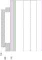
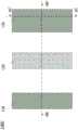
图1为根据本揭露内容的一些实施方式绘示半导体器件的俯视图;FIG. 1 is a top view illustrating a semiconductor device according to some embodiments of the present disclosure;
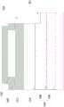
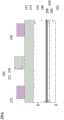
图2A绘示沿着图1中的半导体器件的线段2A-2A’的横截面图;Figure 2A shows a cross-sectional view along
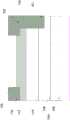
图2B绘示沿着图1中的线段2B-2B’的横截面图;Figure 2B illustrates a cross-sectional view along the
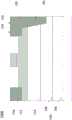
图3绘示根据比较实施方式的半导体器件的横截面示意图;3 shows a schematic cross-sectional view of a semiconductor device according to a comparative embodiment;
图4A-4D是根据本揭露内容的一些实施方式绘示于制造半导体器件的方法中的不同阶段图;4A-4D are diagrams illustrating different stages in a method of manufacturing a semiconductor device according to some embodiments of the present disclosure;
图5为根据本揭露内容的一些实施方式绘示半导体器件的横截面图;5 is a cross-sectional view illustrating a semiconductor device according to some embodiments of the present disclosure;
图6A为根据本揭露内容的一些实施方式绘示半导体器件的俯视图;6A is a top view illustrating a semiconductor device according to some embodiments of the present disclosure;
图6B绘示沿着图6A中的线段6B-6B’的横截面图;Figure 6B shows a cross-sectional view along the
图6C绘示沿着图6A中的线段6C-6C’的横截面图;Figure 6C depicts a cross-sectional view along line 6C-6C' in Figure 6A;
图7为根据本揭露内容的一些实施方式绘示半导体器件的横截面图;7 is a cross-sectional view illustrating a semiconductor device according to some embodiments of the present disclosure;
图8为根据本揭露内容的一些实施方式绘示半导体器件的横截面图;8 is a cross-sectional view illustrating a semiconductor device according to some embodiments of the present disclosure;
图9为根据本揭露内容的一些实施方式绘示半导体器件的横截面图;9 is a cross-sectional view illustrating a semiconductor device according to some embodiments of the present disclosure;
图10绘示根据比较实施方式的半导体器件的横截面示意图;10 shows a schematic cross-sectional view of a semiconductor device according to a comparative embodiment;
图11为根据本揭露内容的一些实施方式绘示半导体器件的横截面图;11 is a cross-sectional view illustrating a semiconductor device according to some embodiments of the present disclosure;
图12A-12C是根据本揭露内容的一些实施方式绘示于制造半导体器件的方法中的不同阶段图;12A-12C are diagrams illustrating different stages in a method of fabricating a semiconductor device according to some embodiments of the present disclosure;
图13为根据本揭露内容的一些实施方式绘示半导体器件的横截面图;13 is a cross-sectional view illustrating a semiconductor device according to some embodiments of the present disclosure;
图14A为根据本揭露内容的一些实施方式绘示半导体器件的横截面图;14A is a cross-sectional view illustrating a semiconductor device according to some embodiments of the present disclosure;
图14B为图14A的缓冲层与屏蔽层的平面图;14B is a plan view of the buffer layer and the shielding layer of FIG. 14A;
图15A-15E是根据本揭露内容的一些实施方式绘示于制造半导体器件的方法中的不同阶段图;15A-15E are diagrams illustrating different stages in a method of fabricating a semiconductor device according to some embodiments of the present disclosure;
图16为根据本揭露内容的一些实施方式绘示半导体器件的横截面图;16 is a cross-sectional view illustrating a semiconductor device according to some embodiments of the present disclosure;
图17A为根据本揭露内容的一些实施方式绘示半导体器件的横截面图;17A is a cross-sectional view illustrating a semiconductor device according to some embodiments of the present disclosure;
图17B为图17A的缓冲层与屏蔽层的平面图;17B is a plan view of the buffer layer and shielding layer of FIG. 17A;
图18A为根据本揭露内容的一些实施方式绘示半导体器件的横截面图;18A is a cross-sectional view illustrating a semiconductor device according to some embodiments of the present disclosure;
图18B为根据本揭露内容的一些实施方式绘示半导体器件的横截面图。18B is a cross-sectional view illustrating a semiconductor device according to some embodiments of the present disclosure.
具体实施方式Detailed ways
于全部的附图和详细说明中,将使用相同的参考符号来表示相同或相似的部件。借由以下结合附图的详细描述,将可容易理解本揭露内容的实施方式。Throughout the drawings and detailed description, the same reference symbols will be used to designate the same or like parts. Embodiments of the present disclosure can be easily understood from the following detailed description in conjunction with the accompanying drawings.
于空间描述中,像是“上”、“下”、“上方”、“左侧”、“右侧”、“下方”、“顶部”、“底部”、“纵向”、“横向”、“一侧”、“较高”、“较低”、“较上”、“之上”、“之下”等的用语,是针对某个组件或是由组件所构成的群组的某个平面定义的,对于组件的定向可如其对应图所示。应当理解,这里使用的空间描述仅用于说明目的,并且在此所描述的结构于实务上的体现可以是以任何方向或方式布置在空间中,对此的前提为,本揭露内容的实施方式的优点不因如此布置而偏离。In spatial descriptions, such as "above", "below", "above", "left", "right", "below", "top", "bottom", "portrait", "landscape", " The terms "one side", "higher", "lower", "upper", "above", "under", etc. refer to a certain component or a certain plane of a group of components defined, the orientation of the components may be as shown in their corresponding figures. It should be understood that the spatial descriptions used herein are for illustrative purposes only and that practical manifestations of the structures described herein may be arranged in any orientation or manner in space provided that embodiments of the present disclosure The advantages of are not deviated from such an arrangement.
此外,需注意的是,对于描绘为近似矩形的各种结构的实际形状,在实际器件中,其可能是弯曲的、具有圆形的边缘、或是具有一些不均匀的厚度等,这是由于设备的制造条件造成的。本揭露内容中,使用直线和直角绘示仅用于方便表示层体和技术特征。In addition, it should be noted that for the actual shape of the various structures depicted as approximately rectangular, in actual devices, it may be curved, have rounded edges, or have some uneven thickness, etc., due to caused by the manufacturing conditions of the equipment. In this disclosure, the use of straight lines and right angles is only used to conveniently represent layers and technical features.
于下面的描述中,半导体器件和其制造方法等被列为优选实例。本领域技术人员将能理解到,可以在不脱离本发明的范围和精神的情况下进行修改,包括添加和/或替换。特定细节可以省略,目的为避免使本发明模糊不清;然而,本揭露内容是为了使本领域技术人员能够在不进行过度实验的情况下,实现本揭露内容中的教示。In the following description, a semiconductor device, its manufacturing method, and the like are listed as preferred examples. Those skilled in the art will appreciate that modifications, including additions and/or substitutions, can be made without departing from the scope and spirit of the present invention. Specific details may be omitted in order to avoid obscuring the present invention; however, this disclosure is intended to enable one skilled in the art to implement the teachings of this disclosure without undue experimentation.
图1为根据本揭露内容的一些实施方式绘示半导体器件100A的俯视图。半导体器件100A包括栅极结构120、一对源极/漏极电极130和136,以构造出晶体管的一部分。源极/漏极电极130和136沿着延伸方向E(即图1中的垂直线)延伸。栅极结构120位于源极/漏极电极130和136之间。在此,俯视图的意思是,对于形成为栅极结构120和源极/漏极电极130和136的层体,是以沿着垂直其的方向观看。FIG. 1 is a top view of a
为了描述,图2A和2B为沿着图1中的半导体器件100A的线段2A-2A’和2B-2B’的横截面图。如图2A所示,半导体器件100A还包括衬底102、缓冲体104、氮化物半导体层110和112以及钝化层126。For description, FIGS. 2A and 2B are cross-sectional views along
衬底102可以是半导体衬底。衬底102的示例性材料例如可包括但不限于硅(Si)、硅锗(SiGe)、碳化硅(SiC)、砷化镓(GaAs)、p型掺杂硅(p-doped Si)、n型掺杂硅(n-dopedSi)、蓝宝石(sapphire)、绝缘体层上覆半导体层,例如绝缘层上覆硅(silicon oninsulator;SOI),或其他适当的半导体材料。在一些实施方式中,衬底102可包括但不限于第三族元素、第四族元素、第五族元素或其组合(例如,III-V化合物)。在其它实施方式中,衬底102可包括(例如但不限于)一个或多个其它特征,例如掺杂区域、埋层、外延(epitaxy)层或其组合。
缓冲体104设置在衬底102上。缓冲体104可用以减少其底下层体与将在缓冲体104上形成的层体(例如,在缓冲体104上外延形成的层体)之间的晶格和热常数不匹配,从而消除由于不匹配/差异而产生的缺陷。缓冲体104可包括III-V族化合物。III-V族化合物可包括,例如但不限于铝、镓、铟、氮或其组合。因此,缓冲体104的示例性材料可进一步包括,例如但不限于,氮化镓(GaN)、氮化铝(AlN)、氮化铝镓(AlGaN)、氮化铝铟镓(AlInGaN)或其组合。The
缓冲体104可以包括由多层层体形成的缓冲体结构。例如,缓冲体104可包括底部106和最顶部108。最顶部108堆叠/形成在底部106上。在底部106和最顶部108之间存在区别得出的界面。在一些实施方式中,底部106和最顶部108可以互相合并,使得其之间的界面外观为无法区分或模糊。The
最顶部108可以包括至少一层层体。底部106可以包括至少一层层体。最顶部108可以包括至少一层层体,其可具有异于底部106的化合物。位在底部106处的层体可以具有第三族元素,并且位在最顶部108处的层体可以不具有此类的第三族元素。例如,位在底部106处的层可以包括铝,而位在最顶部108处的层体不具有铝。位在最顶部108处的层可以是受体掺杂(acceptor-doped)的氮化物半导体化合物。用于受体掺杂的氮化物半导体化合物的至少一种掺杂剂可选自碳、硅、锗、铁或锡中的一种或多种。位在最顶部108处的层体可以是p型氮化物半导体化合物。位在底部106处的层可以是未掺杂的氮化物半导体化合物。在一些实施方式中,最顶部108可包括至少一层的碳掺杂氮化镓,而底部106可包括至少一层的未掺杂铝氮化镓。在一些实施方式中,最顶部108可包括至少一层的铁掺杂氮化镓。The
在一些实施方式中,半导体器件100A可进一步包括成核层(未示出)。成核层可以形成在衬底102和缓冲体104之间。成核层可提供其顶面,以作为用于生长第三族氮化物的材料,从而提供过渡区,以容纳衬底102和将在其顶面上形成的第三族氮化物层(例如,在其上外延形成的缓冲体104)之间的失配/差异。成核层的示例性材料可包括但不限于氮化铝(AlN),或是其合金。In some embodiments, the
氮化物半导体层110设置于缓冲体104上。氮化物半导体层110的示例性材料例如可包括但不限于氮化物或III-V族化合物,例如氮化镓(GaN)、氮化铝(AlN)、氮化铟(InN)、氮化铟铝镓(InxAlyGa(1–x–y)N,其中x+y≤1),氮化铝镓(AlyGa(1–y)N,其中y≤1)。氮化物半导体层112设置于氮化物半导体层110上。氮化物半导体层112的示例性材料可以包括但不限于氮化物或III-V族化合物,例如氮化镓(GaN)、氮化铝(AlN)、氮化铟(InN)、氮化铟铝镓(InxAlyGa(1–x–y)N,其中x+y≤1),氮化铝镓(AlyGa(1–y)N,其中y≤1)。The
可选择性地挑选氮化物半导体层110和112的示例性材料,以使得氮化物半导体层112的带隙(bandgap),或称禁带宽度(forbidden band width),大于氮化物半导体层110的带隙,这将导致其电子亲和力彼此不同。例如,当氮化物半导体层110是未掺杂氮化镓(GaN)层,且其具有约3.4ev的带隙时,氮化物半导体层可以是氮化铝镓(AlGaN)层,且其具有约4.0ev的带隙。因此,氮化物半导体层110和112可分别用作沟道层和势垒层。在沟道层和势垒层之间的键合界面处会产生三角势阱,使得电子积聚在三角势阱中,从而在同一界面处产生二维电子气(two-dimensional electron gas;2DEG)区域114。因此,半导体器件100A可以用作高电子迁移率晶体管(high electron mobility transistor;HEMT)。Exemplary materials of the nitride semiconductor layers 110 and 112 can be selected selectively so that the band gap (bandgap) of the
栅极结构120设置在氮化物半导体层112上。栅极结构120包括p型掺杂III-V化合物半导体层122以及导电栅极124。导电栅极124可以用作栅极电极。p型掺杂III-V化合物半导体层122和导电栅极124堆叠在氮化物半导体层112上。p型掺杂III-V化合物半导体层122位于氮化物半导体层112和导电栅极124之间。在一些实施方式中,栅极结构120可进一步包括介电层(未绘出),其位在氮化物半导体层112和p型掺杂III-V化合物层122之间。在一些实施方式中,栅极结构120还可包括位在p型掺杂III-V化合物层122和导电栅极124之间的介电层(未绘出)。The
半导体器件100A可以是一种增强模式(enhancement mode)器件,当导电栅极124大致处于零偏置时,此增强模式器件会处于常关闭(normally-off)状态。具体而言,p型掺杂III-V化合物半导体层122可与氮化物半导体层112形成p-n结以耗尽2DEG区域114,使得2DEG区域114中对应于栅极结构120下方区域所具有的特性会不同于2DEG区域114的其余部分(例如不同的电子浓度),而因此被阻挡。通过这种机制,半导体器件100A可以具有常闭特性。换言之,当没有电压施加到导电栅极124,或是施加到导电栅极124的电压小于阈值电压(即,在栅极结构120下方形成反转层所需的最小电压)时,2DEG区域114中的位于栅极结构120下方区仍维持着被阻挡,因此,将不会有电流流过此区。此外,通过提供p型掺杂III-V化合物半导体层122,可减小栅极漏电流,并且在关闭状态期间能实现增加阈值电压的效果。The
此外,为了提高具有增强模式半导体器件100A的开关灵敏度,缓冲体104的最顶部108处的层体可以形成为受体掺杂的氮化物半导体化合物或p型氮化物半导体化合物。例如,缓冲体104的最顶部108处的层体可以形成为具有碳掺杂氮化镓化合物的层体。另外,在缓冲体104的最顶部108处的碳掺杂氮化镓化合物层也可以增加半导体器件100A的击穿电压。这里,对于“缓冲体104的最顶部108处的碳掺杂氮化镓化合物层体”,其意思包括氮化物半导体层110会与此碳掺杂氮化镓化合物层体形成界面。In addition, in order to improve the switching sensitivity of the
在一些实施方式中,可以省略p型掺杂III-V化合物半导体层122,使得半导体器件100A是耗尽模式器件,这意思是,半导体器件100A可在栅极源电压为零的情况下,处于常开状态。In some embodiments, the p-type doped III-V
p型掺杂III-V化合物半导体层122的示例性材料例如可包括但不限于,p型掺杂III-V族氮化物半导体材料,像是p型氮化镓(GaN)、p型氮化铝镓(AlGaN)、p型氮化铟(InN)、p型氮化铝铟(AlInN)、p型氮化铟镓(InGaN)、p型氮化铝铟镓(AlInGaN)或其组合。在一些实施方式中,可通过使用p型杂质,像是铍(Be)、镁(Mg)、锌(Zn)、镉(Cd)来实现p型掺杂材料。在一个实施方式中,氮化物半导体层110包括未掺杂氮化镓(GaN),氮化物半导体层112包括氮化铝镓(AlGaN),而p型掺杂III-V化合物半导体层122是p型氮化镓(GaN)层,此p型氮化镓(GaN)层可向上弯曲下方层的能带结构,并耗尽2DEG区域114的相应区,以使半导体器件100A进入关闭状态的条件。在一些实施方式中,导电栅极124的示例性材料例如可包括金属或金属化合物。导电栅极124可以形成为单层层体,或具有相同或不同组份的多层层体。导电栅极124的示例性材料可包括但不限于钨(W)、金(Au)、钯(Pd)、钛(Ti)、钽(Ta)、钴(Co)、镍(Ni)、铂(Pt)、钼(Mo)、氮化钛(TiN)、氮化钽(TaN)、其他金属化合物、氮化物、氧化物、硅化物、掺杂半导体、金属合金或其组合。可选的介电结构例如可包括但不限于一层或多层的介电材料。介电材料的示例性材料可包括但不限于氧化硅(SiOx)层、氮化硅(SiNx)层、高介电常数(high-k)材料,像是二氧化铪(HfO2)、氧化铝(Al2O3)、二氧化钛(TiO2)、锆氧化铪(HfZrO)、氧化钽(Ta2O3)、矽酸铪(HfSiO4)、二氧化锆(ZrO2)、矽酸锆(ZrSiO2)等或其组合。Exemplary materials for the p-type doped III-V
钝化层126设置在氮化物半导体层112上。形成钝化层126可用于保护目的或用于增强器件的电性能。钝化层126覆盖氮化物半导体层112的顶面。钝化层126可至少部分地覆盖栅极结构120。举例而言,钝化层126可至少覆盖栅极结构120的两个彼此相对的侧壁。钝化层126的示例性材料例如可包括但不限于氮化硅(SiNx)、氧化硅(SiOx)、氮氧化硅(SiON)、碳化硅(SiC)、硅硼氮(SiBN)、碳氮硼化硅(SiCBN)、氧化物、氮化物或其组合。在一些实施方式中,钝化层126可以是多层结构,例如氧化铝/氮化硅(Al2O3/SiN)、氧化铝/氧化硅(Al2O3/SiO2)、氮化铝/氮化硅(AlN/SiN)、氮化铝/氧化硅(AlN/SiO2)或其组合的复合介电层体。The
源极/漏极电极130和136设置于氮化物半导体层112上。源极/漏极电极130和136通常可位于钝化层126的相对两侧,然而,也可以使用其他配置,尤其是当器件中使用了多个源极、漏极或栅极电极的时候。源极/漏极电极130和136的侧壁可与钝化层126接触。源极/漏极电极130和136可位于栅极结构120的相对两侧。栅极结构120和源极/漏极电极130和136可以共同作为具有2DEG区域114的氮化镓型高电子迁移率晶体管。Source/
源极/漏极电极130具有的轮廓为,向下延伸至到达缓冲体的最顶部108,其可用于改善动态导通电阻(dynamic on-resistance;Ron)的峰值问题。为了解释为何会发生动态导通电阻的峰值问题,图3绘示根据比较实施方式的半导体器件10的横截面示意图。半导体器件10包括衬底12、缓冲体14、氮化物半导体层16和18、栅极结构20以及一对源极/漏极电极22和24,其中在氮化物半导体层16和18之间的界面会形成2DEG区域。一旦缓冲体14包括了具有p型特性的受体掺杂的氮化物半导体化合物,则缓冲体14和氮化物半导体层16上将会形成寄生p-n结二极管28。在半导体器件10的工作期间,寄生p-n结二极管28将影响2DEG区域的浓度,从而影响动态导通电阻和动态阈值电压(dynamic threshold voltage;Vth)。The source/
更具体而言,半导体器件10的操作可分为低电压区间(例如低于约100伏特)和高电压区间(例如高于约100伏特)。在低电压区间中,若漏极的偏置(Vds)增加,则会使得寄生p-n结二极管28反向偏置,从而耗尽2DEG区域。当Vds进一步增大时,2DEG区的耗尽效应会逐渐增强。因此,动态导通电阻随着Vds的增加而继续增加。在高电压区间中,当Vds增加到一定值时,寄生p-n结二极管28中会发生泄漏;寄生p-n结二极管28的p-n结处的电荷会消失;并且耗尽的2DEG区域会逐渐恢复。因此,动态导通电阻逐渐减小。也就是说,依赖于Vds的动态导通电阻将极大地来自受到寄生p-n结二极管28的影响,并且在低电压区间和高电压区间之间存在一个动态导通电阻峰值,此可称为动态导通电阻的峰值问题;这问题发生在大约100伏特的场合。More specifically, the operation of the
此外,半导体器件10的性能也会取决于动态导通电阻。例如,动态导通电阻将的稳定性将会影响半导体器件的工作效率、工作频率和工作温度。因此,在半导体器件设计中,动态导通电阻将是一个重要因素。这一因素可能主导半导体器件的尺寸,从而导致成本的增加。此外,这一因素也可能与半导体器件的温度有关。一旦半导体器件的温度升高,半导体器件则有可能烧坏或因其他原因而无法工作。动态导通电阻的峰值问题是高电子迁移率晶体管器件领域中的一个需要改进的难题。In addition, the performance of the
请再次参照图2A,源极/漏极电极130具有的轮廓性质异于源极/漏极电极电极136的轮廓性质。这两个电极的轮廓性质相对于栅极结构120不对称。“轮廓性质”的意思可以包括多种性质/属性/特性,如下所述。Referring again to FIG. 2A , the source/
举例而言,对于栅极结构120,源极/漏极电极130具有的形状不同于源极/漏极电极136的形状。在图2A的示例性图示中(即在横截面视图中),源极/漏极电极130的形状近似为L形,并且源极/漏极电极136的形状近似为矩形。For example, for
源极/漏极电极130对于栅极结构120具有的距离差大于源极/漏极电极136对于栅极结构120具有的距离差。在图2A的示例性绘图中,从源极/漏极电极130的底面到栅极结构120的底面的垂直距离大于从源极/漏极电极136的底面到栅极结构120的底面的垂直距离。亦即,对于栅极结构120,源极/漏极电极130的底面比源极/漏极电极136的底面更深。此外,对于栅极结构120,源极/漏极电极的底面比缓冲体104的最顶部108的最顶表面更深。这样,源极/漏极电极130可以比源极/漏极电极136更接近缓冲体104的最顶部108。The source/
源极/漏极电极130和136可视为向下延伸的两个导电电极。钝化层126的顶面可被视为延伸基准面/水平面。源极/漏极电极130向下延伸的长度大于源极/漏极电极136向下延伸的长度。源极/漏极电极130向下延伸到低于氮化物半导体层110的位置。源极/漏极电极136向下延伸到高于氮化物半导体层110的位置。源极/漏极电极130向下延伸到缓冲体104的最顶部108的厚度内的位置。源极/漏极电极136向下延伸到氮化物半导体层112的厚度内的位置。The source/
源极/漏极电极130和136向下延伸,使得源极/漏极电极130具有的最底面会位在低于源极/漏极电极136的位置。源极/漏极电极130的最底面位在低于源极/漏极电极136的整体的位置。源极/漏极电极130和136向下延伸,使得源极/漏极电极136具有的最底面会高于源极/漏极电极130的位置。源极/漏极电极136的最底面的位置至少会高于源极/漏极电极130的至少一部分。由于源极/漏极电极130向下延伸一定程度,故源极/漏极电极130具有的纵向长度可以大于其横向长度。纵向长度指的是沿着垂直于氮化物半导体层110或112的方向,且此方向沿着图2A中的垂直方向。横向长度与纵向长度正交,且其是沿着图2A中的水平方向。此外,源极/漏极电极130的横向长度大于源极/漏极电极136的横向长度。即,源极/漏极电极130和136可以具有不同的宽度。源极/漏极电极130的宽度可以大于源极/漏极电极136的宽度。The source/
源极/漏极电极130可借由自身向下延伸,从而电连接到缓冲体104。源极/漏极电极130可以与缓冲体104的最顶部108形成至少一个界面。源极/漏极电极130可以与缓冲体104的最顶部108中的至少一层的p型氮化物半导体化合物接触。源极/漏极电极130可与缓冲体104的最顶部108中的至少一层的受体掺杂氮化物半导体化合物接触。更具体地说,源极/漏极电极130可向下延伸,从而穿过或穿透氮化物半导体层110和112,并且在缓冲体104的厚度范围内停止。源极/漏极电极130可以在缓冲体104的最顶部108的厚度内停止。The source/
换句话说,源极/漏极电极130是设置在缓冲体104的最顶部108上,并与其接触,且还从低于2DEG区域114的位置向上延伸,直到高于2DEG区域114的位置以及高于氮化物半导体层110和112的位置。因此,源极/漏极电极130具有的侧表面可靠近2DEG区域114,或是也可接触2DEG区域114。另外,源极/漏极电极130可向上延伸,其起始点为自高于缓冲体104的底部106和最顶部108之间的区别得出的界面的位置。In other words, the source/
由于源极/漏极电极130与缓冲体104的最顶部108的层体接触,故源极/漏极电极130与缓冲体104最顶部108中的p-型/受体掺杂化合物电耦合。因此,源极/漏极电极130和缓冲体104的最顶部108中的p型/受体掺杂化合物可以具有相同的电势,或者具有不同但彼此接近的电势。源极/漏极电极130和缓冲体104的最顶部108之间的电位差小于源极/漏极电极136和缓冲体104的最顶部108之间的电位差。也因此,可防止寄生p-n结二极管被反向偏置,从而抑制/避免动态导通电阻峰值的形成,以改进前述于图3阐述的问题。相应地,半导体器件100A的可靠性和性能得到改善。Since the source/
在图2A的示例性绘图中,源极/漏极电极130具有部件132和134。源极/漏极电极130的部件132和134彼此连接,亦即其可通过图案化单个覆盖层而形成。源极/漏极电极130的部件134位于源极/漏极电极136与源极/漏极电极130的部件132之间。部件132具有最底部表面S1A,其位在低于部件134的最底部表面S1B的位置。源极/漏极电极130在部件132和134之间具有拐角轮廓。部件132的最底部表面S1A与缓冲体104的最顶部108可形成界面。具有如此轮廓的源极/漏极电极130的制造过程可以轻易实现,从而产生良好的产率。In the exemplary drawing of FIG. 2A , source/
源极/漏极电极130的部分132还具有侧表面,其与缓冲体104的最顶部108形成至少一个界面,以增加了源极/漏极电极130和缓冲体104的最顶部108之间的接触面积。源极/漏极电极130的部件132的侧表面和最底表面S1A可以具有一个共用边缘。例如,源极/漏极电极130的部件132的侧表面和最底面S1A分别是垂直的和水平的,且其在同一边缘处重合。源极/漏极电极130的部件132的侧表面也可以与氮化物半导体层110和112形成界面。The
在图2A的示例性绘图中,右边的源极/漏极电极130和左边的源极/漏极电极136可分别用作漏极和源极。源极/漏极电极130和136可任选地,对于栅极结构120为不对称的。在一些实施方式中,源极/漏极电极130比源极/漏极电极136更接近栅极结构120。在其它实施方式中,源极/漏极电极136比源极/漏极电极130更接近栅极结构120。In the exemplary drawing of FIG. 2A , the right source/
在一些实施方式中,源极/漏极电极130和136可以包括但不限于金属、合金、掺杂半导体材料(例如掺杂的晶体硅)、像是硅化物和氮化物的化合物、其他导体材料或其组合。源极/漏极电极130和136的示例性材料可以包括例如但不限于钛(Ti)、铝硅(AlSi)、氮化钛(TiN)或其组合。源极/漏极电极130和136可以是单层的,或是具有相同或不同组份的多层体。在一些实施方式中,源极/漏极电极130与缓冲体104的最顶部108形成欧姆接触。在一些实施方式中,源极/漏极电极136与氮化物半导体层112形成欧姆接触。欧姆接触可以通过在源极/漏极电极130和136上施加钛、铝或其它合适的材料来实现。In some embodiments, source/
图2B绘示沿着图1中的线段2B-2B‘的横截面图。缓冲体104的最顶部108具有至少一个凹槽R1。缓冲体104的凹槽R1可以接收源极/漏极电极130。源极/漏极电极130还具有至少一个向下延伸部130E,其位在凹槽R1中。向下延伸部130E的末端部可被缓冲体104的最顶部108包围。凹槽R1可包围向下延伸部130E,并具有逐渐狭窄的边界。在其它实施方式中,凹槽R1包围向下延伸部130E,并具有垂直的边界。FIG. 2B is a cross-sectional view along
除凹槽R1外,氮化物半导体层110和112可与缓冲体104的最顶部108共同具有至少一个凹槽R2,以接收源极/漏极电极130。向下延伸部130E可完全地填充到凹槽R2中。可由氮化物半导体层110和112以及缓冲体104的最顶部108共同定义及限定出凹槽R2具有的至少一个侧壁SW。侧壁SW包围/围绕向下延伸部130E。对于缓冲体104的最顶部108和向下延伸部130E之间的界面,侧壁SW与此界面可形成钝角。In addition to the groove R1 , the nitride semiconductor layers 110 and 112 may have at least one groove R2 in common with the topmost 108 of the
对于上述源极/漏极电极130的轮廓,由于不必引入复杂的制造工艺就可实现,故半导体器件100A的制造工艺的成品率不会因轮廓需求而受到影响。也就是说,可以在不用牺牲产率的情况下,就使源极/漏极电极130具有前述轮廓。用于制造半导体器件100A的方法的不同阶段在图中示出,如图4A-4D及以下与其相关的描述。The above profile of the source/
请参照图4A,先准备衬底102。于衬底102上方,可依序形成缓冲体104、氮化物半导体层110和112。缓冲体104包括底部106和最顶部108,其可通过沉积工艺依序形成在衬底102上。氮化物半导体层110和112可通过沉积工艺依序形成在衬底102上。沉积工艺例如可包括但不限定于原子层沉积(atomic layer deposition;ALD)、物理气相沉积(physicalvapor deposition;PVD)、化学气相沉积(chemical vapor deposition;CVD)、金属有机化学气相沉积(metal organic chemical vapor deposition;MOCVD)、等离子体辅助气相沉积、外延生长(epitaxial growth),或其他合适的过程来实现。Referring to FIG. 4A , the
请参照图4B,可形成钝化层126以覆盖氮化物半导体层112。可形成保护层140以覆盖钝化层126。保护层140可作为移除过程(例如刻蚀过程)中的掩模层。保护层140与钝化层126共形。保护层140还进一步覆盖钝化层126的两个相对侧壁。氮化物半导体层112的至少一个区域可从保护层140暴露出来。钝化层126和保护层140的形成方式均可以通过使用沉积技术来实现。沉积技术例如可包括但不限于,原子层沉积、物理气相沉积、化学气相沉积、金属有机化学气相沉积、外延生长或其他合适的工艺来实现。Referring to FIG. 4B , a
请参照图4C,可在氮化物半导体层110和112中形成穿孔TH。可移除氮化物半导体层110的一部分和氮化物半导体层112的一部分,以形成穿孔TH。还可进一步移除缓冲体104的最顶部108的一部分。可移除缓冲体104的最顶部108的一部分,以使得在穿孔TH下方形成凹槽R1。凹槽R1和穿孔TH可共同称为深凹槽。穿孔TH和凹槽R1的位置对应于氮化物半导体层112自保护层140暴露的区域,如图4B所示。实现移除的方式例如可通过但不限于刻蚀技术(即刻蚀工艺,例如干刻蚀或湿刻蚀)来执行,激光技术(激光钻或激光切割)或其他合适的技术。Referring to FIG. 4C , through holes TH may be formed in the nitride semiconductor layers 110 and 112 . A portion of the
请参照图4D,可去除保护层140,并形成源极/漏极电极130和136。可将源极/漏极电极130形成在穿孔TH和凹槽R1中。源极/漏极电极130可与缓冲体104的被暴露出的最顶部108(即,如图4C所示的,其从凹槽R1暴露)形成界面。部分的源极/漏极电极130和136会位于比氮化物半导体层112的最顶表面还低的位置。在一些实施方式中,可移除部分的氮化物半导体层112以形成凹槽/沟槽,其可接收源极/漏极电极130和136的底部。在一些实施方式中,当形成钝化层126时,可以在钝化层126上执行图案化处理,以定义且限定出用于形成源极/漏极电极130和136的源极/漏极区域。在图案化过程中,部分的氮化物半导体层112也会被移除,因此会在源极/漏极区域形成凹陷/沟槽,其可用于接收源极/漏极电极130和136的底部。在一些实施方式中,源极/漏极130和136的形成方式包括沉积技术工艺以及一系列的光刻工艺。沉积工艺可以包括,例如但不限于,原子层沉积、物理气相沉积、化学气相沉积、金属有机化学气相沉积、外延生长或其他合适的工艺。一系列的光刻工艺可包括施加光阻层、刻蚀、显影和/或其它合适的工艺,从而能图案化所形成的源极/漏极电极130和136。Referring to FIG. 4D, the
在图4D所示的阶段后,可以在氮化物半导体层110和112上方形成栅极结构,从而获得前述结构。在一些实施方式中,栅极结构可以形成在钝化层126中。也就是说,可以在钝化层126中形成凹槽/沟槽,并且将栅极结构形成为填充凹陷/沟槽。在其它实施例中,可以在全部或一部分的钝化层126上形成栅极结构。栅极结构的形成过程包括依次进行的形成p型掺杂III-V化合物层和形成导电栅极。栅极结构的形成方式可以通过使用沉积技术和一系列的光刻工艺来实现。沉积技术例如可以包括但不限于,原子层沉积、物理气相沉积、化学气相沉积、金属有机化学气相沉积、外延生长或其他合适的工艺。一系列的光刻工艺包括施加光阻层、刻蚀、显影和/或其它合适的工艺。After the stage shown in FIG. 4D, a gate structure may be formed over the nitride semiconductor layers 110 and 112, thereby obtaining the aforementioned structure. In some implementations, a gate structure may be formed in the
图5为根据本揭露内容的一些实施方式绘示半导体器件100B的横截面图。在本实施方式中,如图5的示例性绘图所示,源极/漏极电极130的部件132形成为具有倾斜的侧壁(即,比源极/漏极电极136的侧壁更倾斜)。更具体地说,凹槽R2的至少一个侧壁可由氮化物半导体层110和112以及缓冲体104的最顶部108定义及限定。凹槽R2的侧壁可对源极/漏极电极130的部件132与缓冲体104的最顶部108之间的界面形成钝角。对应于凹槽R2的侧壁的轮廓,填充在凹槽R2内的源极/漏极电极130的部件132可具有倾斜的侧壁。源极/漏极电极130的部件132和134之间的夹角是钝角。在将凹槽R2形成为具有倾斜的侧壁的情况下,仍可改善动态导通电阻的峰值问题,因此半导体器件的制造工艺是灵活的。FIG. 5 is a cross-sectional view illustrating a
图6A为根据本揭露内容的一些实施方式绘示半导体器件的俯视图,而图6B及图6C分别绘示沿着图6A中的线段6B-6B‘及线段6C-6C’的横截面图。在本实施方式中,如图6B的示例性绘图所示,源极/漏极电极130的部件132具有底面S1A,其可与缓冲体104的最顶部108形成界面,且源极/漏极电极130的部件132还具有比底面S1A高的底面S1C。底面S1C与氮化物半导体层112形成至少一个界面。部件134具有底面S1B,其可与氮化物半导体层112形成界面。底面S1B和S1C可位于相同的水平高度。底面S1B和S1C可以彼此共面。在图6C的示例性绘示中,源极/漏极电极130的部件132具有多个向下延伸部130E,其位在多个凹槽R1中。多个向下延伸部130E可分别与缓冲体104的最顶部108形成界面。向下延伸部130E沿延伸方向E设置。向下延伸部130E与缓冲体104的最顶部108之间的界面也沿延伸方向E设置。至少一部分的氮化物半导体层112,至少一部分的氮化物半导体层110,以及至少一部分的缓冲体104的最顶部108可位于两个向下延伸部130E之间。在将源极/漏极电极130的部件132形成为具有多个向下延伸部130E的情况下,仍可改善动态导通电阻的峰值问题,因此半导体器件的制造工艺是灵活的。6A is a top view of a semiconductor device according to some embodiments of the present disclosure, and FIGS. 6B and 6C are cross-sectional views along
图7为根据本揭露内容的一些实施方式绘示半导体器件100D的横截面图。在本实施方式中,如图7的示例性绘图所示,半导体器件100D还包括布置在高电子迁移率晶体管器件上的附加层。半导体器件100D还包括钝化层150、通孔152和图案化导电层154。FIG. 7 is a cross-sectional view of a
钝化层150设置在钝化层126上。钝化层150覆盖钝化层126、栅极结构120以及源极/漏极电极130和136。钝化层150的示例性材料例如可包括但不限于氮化硅(SiNx)、氧化硅(SiOx)、氮氧化硅(SiON)、碳化硅(SiC)、硅硼氮(SiBN)、碳氮硼化硅(SiCBN)、氧化物、氮化物或其组合。在一些实施方式中,钝化层126可以是多层结构,例如氧化铝/氮化硅(Al2O3/SiN)、氧化铝/氧化硅(Al2O3/SiO2)、氮化铝/氮化硅(AlN/SiN)、氮化铝/氧化硅(AlN/SiO2)或其组合的复合介电层体。在一些实施例中,钝化层150可通过使用沉积技术形成。沉积技术例如可以包括但不限于原子层沉积、物理气相沉积、化学气相沉积、金属有机化学气相沉积、外延生长或其他合适的工艺。
通孔152设置在钝化层150内。通孔152可穿过钝化层150。通孔152可纵向延伸,以分别与栅极结构120、源极/漏极电极130和136电气耦合。通孔152的顶部可未受钝化层150的覆盖。通孔152的示例性材料例如可包括但不限于导电材料,金属或合金。通孔152的形成方式可包括在钝化层150内部和上方形成导电层,并移除导电层的多余部分。在一些实施方式中,可执行平坦化过程以移除导电层的多余部分。在一些实施方式中,平坦化工艺包括化学机械抛光(CMP)工艺。
图案化导电层154设置在钝化层150和通孔152上。图案化导电层154与通孔152接触。图案化导电层154的形成方式包括通过使用沉积技术,以在钝化层150上形成一整层导电层。沉积技术例如可以包括但不限于,原子层沉积、物理气相沉积、化学气相沉积、金属有机化学气相沉积、外延生长或其他合适的工艺。可对一整层导电层进行图案化处理,以形成图案化导电层154,此图案化导电层154可包括分别与通孔152接触的金属线。图案化处理可以通过光刻、曝光和显影、刻蚀、其他合适的过程或其组合来实现。在一些实施方式中,图案化导电层154还可用作导电垫或走线。A patterned
图8为根据本揭露内容的一些实施方式绘示半导体器件100E的横截面图。在本实施方式中,如图8的示例性绘图所示,栅极结构120设置在钝化层126上。栅极结构120被钝化层150覆盖。电气连接于栅极结构120和图案化导电层154之间的通孔152比其他通孔152短。FIG. 8 is a cross-sectional view illustrating a
图9为根据本揭露内容的一些实施方式绘示半导体器件100F的横截面图。在本实施方式中,如图9的示例性绘图所示,源极/漏极电极160和162位于栅极结构120的相对两侧,其中源极/漏极电极160与缓冲体104的最顶部108形成至少一个界面。源极/漏极电极160和162的配置相对于栅极结构120是不对称的。更具体地,源极/漏极电极160和162各自均是由至少一个共形层和导电填充物形成。源极/漏极电极160的共形层和导电填充物具有的特征可异于源极/漏极电极162的特征,因此其被称为“相对于栅极结构120是不对称的”。FIG. 9 is a cross-sectional view illustrating a
源极/漏极电极160包括共形层160A、160B、160C、160D和导电填充物160E。共形层160A-160D和导电填充物160E从缓冲体104的最顶部108依次堆叠。源极/漏极电极162包括共形层162A、162B、162C、162D和导电填充物160E。共形层162A-162D和导电填充物162E从氮化物半导体层112堆叠。Source/
共形层160A和162A可以具有相同的材料。共形层160A和162A可以是先形成一整层的层体,然后再经由图案化此层体而形成。对此,共形层160A可以向下延伸到比共形层162A更低的位置,这使得共形层160A的厚度小于共形层162A的厚度。例如,一部分的共形层160A是沿着氮化物半导体层110、112的侧壁以及缓冲体104的最顶部108延伸,且此一部分的厚度可以小于一部分的共形层162A的厚度,此一部分的共形层162A为沿着氮化物半导体层112的侧壁延伸。共形层160A和162A可以延伸并改变方向。共形层160A可在缓冲体104的最顶部108处延伸并改变方向,以使其具有的轮廓异于共形层162A的轮廓。
共形层160A和162A之间的关系可套用于共形层160B和162B之间、共形层160C和162C之间或共形层160D和162D之间的关系。共形层160A或162A的示例性材料例如可包括但不限于钛(Ti)、钽(Ta)或其组合。共形层160B或162B的示例性材料例如可包括但不限于铝(Al)、铝硅(AlSi)或其组合。共形层160C或162C的示例性材料例如可包括但不限于钛(Ti)、镍(Ni)、铂(Pt)或其组合。共形层160D或162D的示例性材料例如可包括但不限于氮化钛(TiN)、铜(Au)或其组合。The relationship between
导电填充物160E和162E可以具有相同的材料。导电填充物160E或162E的示例性材料例如可包括但不限于铝硅(AlSi)、铝铜(AlCu)或其组合。导电填充物160E和162E可以通过形成单层层体,接着在此单层层体上进行平坦化处理来形成。对此,导电填充物160E可进一步向下延伸至低于导电填充物162E的位置,这使得导电填充物160E具有大于导电填充物162E的厚度。此外,由于共形层160A-160D共同具有的轮廓不同于共形层162A-162D的轮廓,因此导电填充物160E和162E可具有不同的形状。导电填充物160E在横截面图中可以近似为T形。导电填充物162E在横截面图中可以近似为矩形。The
总体而言,上述实施方式为提供一种半导体器件,其包括与缓冲体最顶部接触的源极/漏极电极,以使电极与缓冲体电气耦合。上述实施方式描述了具有不同配置的半导体器件。这些实施方式不是相互排斥的,即其可相互搭配。例如,图8所示的通孔和导电层可以应用于图9所示的结构。In general, the above embodiments provide a semiconductor device, which includes a source/drain electrode in contact with the top of the buffer body, so that the electrode is electrically coupled with the buffer body. The above-described embodiments describe semiconductor devices having different configurations. These embodiments are not mutually exclusive, ie they can be combined with each other. For example, the via hole and conductive layer shown in FIG. 8 can be applied to the structure shown in FIG. 9 .
除了寄生p-n结二极管外,缓冲体中的缺陷也可能影响2DEG区域,且还进一步影响动态导通电阻的峰值问题。为了说明这种影响,图10绘示根据比较实施方式的半导体器件30的横截面示意图。半导体器件30包括衬底32、缓冲体34、氮化物半导体层36和38、栅极结构30以及一对源极/漏极电极32和34,其中在氮化物半导体层36和38之间的界面处会形成2DEG区域。缓冲体34内部可能带有缺陷40。在半导体领域中,由于工艺的变化或差异,缺陷几乎是不可避免的。缺陷40会成为自由电子或空穴的吸引中心,这将进一步影响2DEG区域的浓度。In addition to parasitic p-n junction diodes, defects in the buffer body may also affect the 2DEG region, and further affect the peak value of the dynamic on-resistance. To illustrate this effect, FIG. 10 shows a schematic cross-sectional view of a
由于此类缺陷不涉及“偏置”(或反向偏置)或寄生p-n结二极管,因此半导体器件30在宽电压范围内的操作都会受到影响。例如,寄生p-n结二极管可在约100V下影响半导体器件。然而,半导体器件30在0V到约800V(或更大)之间的电压范围内,都会受到缺陷40的影响。也就是说,在半导体器件30的整个工作范围内,缺陷40将进一步影响半导体器件30的性能。Since such defects do not involve "biasing" (or reverse biasing) or parasitic p-n junction diodes, the operation of
图11为根据本揭露内容的一些实施方式绘示半导体器件200A的横截面图。半导体器件200A包括衬底202、缓冲体204、氮化物半导体层210、212、栅极结构220、一对源极/漏极电极230和232以及屏蔽层240。FIG. 11 is a cross-sectional view illustrating a
衬底202可以与前述衬底102相同或相似。缓冲体204包括底部206和最顶部208,其可以与前述的缓冲体104相同或相似。在一些实施方式中,可以省略最顶部208,使得缓冲体204的最顶表面将是与底部206重合。The
氮化物半导体层210、212设置在缓冲体204上。氮化物半导体层210、212的示例性材料可以与前述氮化物半导体层110、112的示例性材料相同或相似,以便于其之间形成2DEG区域214。The nitride semiconductor layers 210 and 212 are provided on the
栅极结构220设置在氮化物半导体层212上。可优选地,栅极结构220包括p型掺杂III-V化合物半导体层222和导电栅极224,其可以与前述的p型掺杂III-V化合物半导体层122和导电栅极124相同或相似。P型掺杂III-V化合物半导体层222可为半导体器件200A提供增强模式。源极/漏极电极230和232设置在氮化物半导体层212上,并且位于栅极结构220的相对两侧。栅极结构220以及源极/漏极电极230和232可共同作为具有2DEG区域214的HEMT器件。The
为了使图11的绘图不过于复杂,源极/漏极电极230和232位于氮化物半导体层212上方且未向下延伸,但是本揭露内容不限于此。在其他实施方式中,可以将向下延伸的源极/漏极电极230引入至图11的示例性绘图中,或者是,可以将本揭露内容的其他结构配置结合至图11应用。In order to make the drawing of FIG. 11 not too complicated, the source/
屏蔽层240设置在缓冲体204和氮化物半导体层210之间。如前所述,会因缓冲体204的性质,而产生寄生p-n结二极管,或是其包括的缺陷会作为自由电子或空穴吸引中心。为了消除如此的缺陷,可形成屏蔽层240,其可以切断从缓冲体204到氮化物半导体层210的电气路径/载子路径。The
屏蔽层240的示例性材料可经选择,使得其具有的带隙会比缓冲体204和氮化物半导体层210的带隙更大,以便作为这些层体之间的电气屏蔽层/电气隔离区域。屏蔽层240可包括隔离化合物。隔离化合物的带隙可以大于缓冲体204的带隙。隔离化合物的带隙可以大于氮化物半导体层210的带隙。隔离化合物的带隙可以大于氮化物半导体层212的带隙。此外,由于屏蔽层240与氮化物半导体层210直接接触,因此隔离化合物必须使氮化物半导体层210能够在其上成长。Exemplary materials of the
为满足这些需求特征,在一些实施方式中,隔离化合物可至少由包含至少一种金属元素的近似二维材料层制成。二维材料层可以形成为原子薄膜,其能够实现单原子层厚或双原子层厚的层体。这样的薄膜将允许氮化物层(例如氮化镓层或氮化铝镓层)在其上外延生长。这是因为单原子层厚或双原子层厚够薄,其足以使氮化物层能在二维材料上直接生长形成,然而同时会稍微牺牲了位错(即,位错可能略微增加)。此外,单原子层厚或双原子层厚的层体的二维材料可以用作台阶,其可以促进氮化镓进行台阶生长,从而使氮化镓能够在其上外延生长。对此,尽管位错可能会略微增加,但因改善动态导通电阻的峰值问题所带来的正面效益大于位错略微增加所带来的负面影响。因此,通过使用屏蔽层240,可提高半导体器件200A的性能。To meet these required characteristics, in some embodiments, the spacer compound can be made at least from a layer of an approximately two-dimensional material comprising at least one metal element. Two-dimensional material layers can be formed as atomic thin films, which can realize monoatomic or diatomically thick layers. Such a thin film would allow a nitride layer, such as a gallium nitride layer or an aluminum gallium nitride layer, to grow epitaxially thereon. This is because the monoatomic or biatomic thickness is thin enough to enable the direct growth of nitride layers on 2D materials, while at the same time slightly sacrificing dislocations (ie, dislocations may increase slightly). In addition, two-dimensional materials with one-atom or two-atom-thick layers can be used as steps, which can facilitate the step growth of GaN, thereby enabling epitaxial growth of GaN on it. In this regard, although dislocations may increase slightly, the positive benefit of improving the peak value of the dynamic on-resistance is greater than the negative impact of a slight increase in dislocations. Therefore, by using the
在一些实施方式中,关于具有上述特征的二维材料,可以选择二元化合物作为隔离化合物,其中金属组份包括硼、锆或铪。隔离化合物例如可为氮化硼(BN)、五碲化锆(ZrTe5)或五碲化铪(HfTe5),但不限于此。关于屏蔽层240的厚度,屏蔽层240实质上可比缓冲体204以及氮化物半导体层210和212薄。在一些实施方式中,屏蔽层240具有的厚度会在约0.01纳米至约1纳米的范围内。In some embodiments, with regard to the two-dimensional materials with the above characteristics, a binary compound can be selected as the spacer compound, wherein the metal component includes boron, zirconium or hafnium. The isolation compound can be, for example, boron nitride (BN), zirconium pentatelluride (ZrTe5 ) or hafnium pentatelluride (HfTe5 ), but is not limited thereto. Regarding the thickness of the
除了选择二维材料来形成屏蔽层240之外,还可以将包括第三族元素和氧元素的隔离化合物应用在屏蔽层240上。第三族元素可提供关于晶格匹配的贡献,以利于在屏蔽层240上直接形成氮化物层。氧元素可与第三族元素结合,以使屏蔽层240具有电隔离特性。在这种配置中,屏蔽层240可具有由氧化铝(Al2O3)或氮氧化铝(AlON)制成的隔离化合物。In addition to selecting two-dimensional materials to form the
简而言之,可否在屏蔽层240上直接形成氮化物半导体层210的两个因素包括对屏蔽层240的材料选择和厚度。In short, two factors that determine whether the
在缓冲体204的最顶部208包括掺杂氮化物半导体化合物的实施例中,屏蔽层240可以不含镓,并且被插入到包括镓的层体之间。例如,如果缓冲体204的最顶部208中的掺杂氮化物半导体化合物是掺杂氮化镓半导体化合物,并且氮化物半导体层210和212也包括镓,则屏蔽层240可以不具有镓。在一些实施方式中,掺杂氮化物半导体化合物的掺杂剂至少是选自碳、硅、锗或锡中的一种或多种。In embodiments where the topmost 208 of the
形成屏蔽层240的目的是减少缓冲体204对2DEG区域214造成的影响。也就是说,对于2DEG区域214内,从源极/漏极电极232通过栅极结构220,再到源极/漏极电极230的路径,屏蔽层240可采对应于此路径的方式,插入至缓冲体204与氮化物半导体层210之间。The purpose of forming the
栅极结构220和源极/漏极电极230和232可直接位于屏蔽层240上方。栅极结构220和源极/漏极电极230和232于缓冲体204上的垂直投影会完全落在屏蔽层240于缓冲体204上的垂直投影内。因此,从源极/漏极电极232经由2DEG区域214到栅极结构220的路径也会直接位在屏蔽层240的上方。从栅极结构220经由2DEG区域214到源极/漏极电极230的路径也会直接位在屏蔽层240的上方。此外,从缓冲体204到2DEG区域214的路径会与屏蔽层240至少部分地重叠。
在缓冲体204、屏蔽层240和氮化物半导体层210之间的关系中,屏蔽层240可以与另外两个层体接触。屏蔽层240可与缓冲体204的最顶表面形成界面I1。屏蔽层240可与氮化物半导体层210的最底表面形成界面I2。界面I1和I2可以通过屏蔽层240彼此分离。在一些实施方式中,屏蔽层240完全覆盖缓冲体204的最顶表面,使得界面I1和I2通过屏蔽层240彼此完全分离,从而进一步增强电气隔离效果。亦即,缓冲体204的最顶表面可通过屏蔽层240而与氮化物半导体层210的最底表面完全分离。In the relationship between the
通过这种配置,屏蔽层240可以阻挡缓冲体204对氮化物半导体层210造成的影响。因此,可避免产生跨越缓冲体204和氮化物半导体层210的潜在寄生p-n结二极管。此外,若缓冲体204中有缺陷,则也可被屏蔽层240阻挡,这将有利于改善动态导通电阻峰值问题。With this configuration, the
由于制造半导体器件200A的制程不会过于复杂,故可维持其制造成品率。图12A-12C示出了用于制造半导体器件200A的方法的不同阶段。Since the manufacturing process of the
参照图12A,可提供衬底202。在衬底202上方形成缓冲体204。缓冲体204包括底部206和最顶部208,其可通过使用沉积技术,在衬底202上方依序形成。沉积技术例如可包括但不限于原子层沉积、物理气相沉积、化学气相沉积、金属有机化学气相沉积、外延生长或其他合适的工艺来实现。在一些实施例中,可以省略最顶部208,而形成缓冲体204的步骤将会在底部206的生长结束时终止。Referring to Figure 12A, a
参照图12B,可在缓冲体204上/上方形成屏蔽层240。屏蔽层240可形成为与缓冲体204接触,以便与缓冲体204形成界面。屏蔽层240可形成为一层覆盖层,以完全地覆盖缓冲体204。这样,缓冲体204的最顶表面会被屏蔽层240完全覆盖。屏蔽层240的形成方式可以通过使用沉积技术来实现。沉积技术例如可包括但不限于原子层沉积、物理气相沉积、化学气相沉积、金属有机化学气相沉积、外延生长或其他合适的工艺来实现。屏蔽层240可以通过沉积技术,由至少一种如前述二维材料制成的隔离化合物来形成。Referring to FIG. 12B , a
参照图12C,可在屏蔽层240上形成氮化物半导体层210。所形成的氮化物半导体层210会借由屏蔽层240而与缓冲体204分离。氮化物半导体层210可直接从屏蔽层240生长。所形成的氮化物半导体层210可具有所需的厚度。可以通过使用沉积技术来形成氮化物半导体层210。沉积技术例如可包括但不限于原子层沉积、物理气相沉积、化学气相沉积、金属有机化学气相沉积、外延生长或其他合适的工艺来实现。Referring to FIG. 12C , the
在形成氮化物半导体层210之后,可以在氮化物半导体层210之上/上/上方形成栅极结构220、一对源极/漏极电极230和232,其可与前述的过程类似。After the
图13为根据本揭露内容的一些实施方式绘示半导体器件200B的横截面图。在本实施方式中,如图13的示例性绘图所示,可在氮化物半导体层212上形成钝化层242和244、通孔250和图案化导电层252。所形成的钝化层242覆盖氮化物半导体层212和栅极结构220。源极/漏极电极230和232穿过钝化层242,并与氮化物半导体层212接触。钝化层244设置在钝化层242上。钝化层244覆盖钝化层242和源极/漏极电极230和232。FIG. 13 is a cross-sectional view illustrating a
尽管形成钝化层242和244的主要目的是为了电气隔离,(例如,为了电气隔离底层和上层),这与形成屏蔽层240的原因相似,然而,钝化层242和244具有的材料可以不同于屏蔽层240。对此,钝化层242和244包括的隔离化合物可与屏蔽层240中使用的隔离化合物不同。例如,在一些实施方式中,屏蔽层240可以包括硼,然而钝化层242和244未包括硼。在一些实施方式中,钝化层242和244中的至少一个层体可以包括硅(例如,SiNx、SiOx、SiON、SiC),而屏蔽层240未包括硅。此外,所形成的屏蔽层240的厚度基本上小于钝化层242和244中的至少一个层体。钝化层242或244的示例性材料例如可包括但不限于氮化硅(SiNx)、氧化硅(SiOx)、氮氧化硅(SiON)、碳化硅(SiC)、硅硼氮(SiBN)、碳氮硼化硅(SiCBN)、氧化物、氮化物或其组合。在一些实施方式中,钝化层242或244可以是多层结构,例如氧化铝/氮化硅(Al2O3/SiN)、氧化铝/氧化硅(Al2O3/SiO2)、氮化铝/氮化硅(AlN/SiN)、氮化铝/氧化硅(AlN/SiO2)或其组合的复合介电层体。在一些实施方式中,钝化层242或244可通过使用沉积技术形成。沉积技术例如可以包括但不限于原子层沉积、物理气相沉积、化学气相沉积、金属有机化学气相沉积、外延生长或其他合适的工艺。Although the primary purpose of forming
通孔250设置在钝化层244内。通孔250可穿过钝化层244。通孔250可纵向延伸,以分别与栅极结构220、源极/漏极电极230和232电气耦合。通孔250的顶部可未受钝化层244的覆盖。通孔250的示例性材料例如可包括但不限于导电材料,金属或合金。通孔250的形成方式可包括在钝化层244内部和上方形成导电层,并移除导电层的多余部分。在一些实施方式中,可执行平坦化过程以移除导电层的多余部分。在一些实施方式中,平坦化工艺包括化学机械抛光(CMP)工艺。
图案化导电层252设置在钝化层244和通孔250上。图案化导电层252与通孔250接触。图案化导电层252的形成方式包括通过使用沉积技术,以在钝化层244上形成一整层导电层。沉积技术例如可以包括但不限于,原子层沉积、物理气相沉积、化学气相沉积、金属有机化学气相沉积、外延生长或其他合适的工艺。可对一整层导电层进行图案化处理,以形成图案化导电层252,此图案化导电层252可包括分别与通孔250接触的金属线。图案化处理可以通过光刻、曝光和显影、刻蚀、其他合适的过程或其组合来实现。在一些实施方式中,图案化导电层252还可用作导电垫或走线。A patterned
图14A为根据本揭露内容的一些实施方式绘示半导体器件200C的横截面图。半导体器件200C包括衬底202、缓冲体204、氮化物半导体层210、212、栅极结构220、一对源极/漏极电极230和232以及屏蔽层260。在半导体器件200C的配置中,对于衬底202、缓冲体204、氮化物半导体层210、212、栅极结构220以及源极/漏极电极230和232的配置可以与前述的半导体器件200A的配置相同或类似。在一些实施方式中,可以省略最顶部208,并且缓冲体204的最顶表面会与底部206重合。FIG. 14A is a cross-sectional view of a
屏蔽层260可插入至缓冲体204和氮化物半导体层210之间。形成屏蔽层260是为了消除缺陷,像是寄生p-n结二极管的行程或层体内缺陷的形成,从而减轻动态导通电阻的峰值问题。The
在屏蔽层260的材料选择方面,其示例性材料可被选择为具有的带隙比缓冲体204和氮化物半导体层210的带隙更大,以便充当缓冲体204和氮化物半导体层210之间的电气屏蔽层/电气隔离区域。屏蔽层260包括隔离化合物。隔离化合物的带隙可以大于缓冲体204的带隙。隔离化合物的带隙可以大于氮化物半导体层210的带隙。隔离化合物的带隙可以大于氮化物半导体层212的带隙。In terms of material selection for the
在图14A的示例性绘图中,在屏蔽层260的材料选择方面有较多选择,这是因为氮化物半导体层210可以借由缓冲体204进行生长。更具体地说,请参照图14B,其为图14A的缓冲体204与屏蔽层260的平面图,且对其的观察方向是沿着垂直于衬底202的方向,然后看向屏蔽层260和缓冲体204。屏蔽层260具有多个孔262以暴露出缓冲体204。缓冲体204的最顶表面的一些部分会被屏蔽层260覆盖。亦即,隔离层屏蔽层260具有的至少一个内边界可围绕缓冲体204。屏蔽层260可以被称为图案化层。每个孔262可以被排列为具有间隔264。In the exemplary drawing of FIG. 14A , there are more choices in material selection of the
请回到图14A,缓冲体204和氮化物半导体层210可通过孔262的间隔264,而与彼此形成至少一个界面205。Please return to FIG. 14A , the
也就是说,氮化物半导体层210可以利用界面205处的缓冲体204进行生长,这意味着氮化物半导体层210的生长并非完全取决于屏蔽层260的特性。因此,屏蔽层260可由隔离化合物制成,该隔离化合物可包括但不限于二氧化硅(SiO2)、氮化硅(SiN)、三氧化二铝(Al2O3)、氮氧化铝(AlON)或其它电绝缘材料。在一些实施方式中,隔离化合物由至少一种介电材料制成,使得屏蔽层260的电阻大于缓冲体204或氮化物半导体层210的电阻,亦即,屏蔽层260的电导率小于缓冲体204或氮化物的半导体层210的电导率。That is, the
在涉及缓冲体204的最顶部208包括掺杂氮化物半导体化合物的一些实施方式中,屏蔽层260可以不含镓,且其被插入至有包括镓的层体之间。例如,当缓冲体204的最顶部208中的掺杂氮化物半导体化合物是掺杂氮化镓半导体化合物,且氮化物半导体层210和212也包括镓时,屏蔽层260可以没有镓。在一些实施方式中,掺杂氮化物半导体化合物的至少一种掺杂剂可选自碳、硅、锗或锡中的一种或多种。屏蔽层260可以具有弹性的厚度范围。在一些实施例中,屏蔽层260的厚度在约1纳米到约100纳米的范围内。In some embodiments involving the topmost 208 of the
屏蔽层260可用作缓冲体204与氮化物半导体层210之间的电气隔离区,以改善动态动态导通电阻的峰值问题。此外,在氮化物半导体层210的生长期间,随着氮化物半导体层210生长,其会逐渐填充孔262的间隔264。当氮化物半导体层210在屏蔽层260上方的位置继续生长时,氮化物半导体层210会开始在屏蔽层260上方进行横向外延生长。这种方法的优点是缓冲体204中的任何位错线(即缓冲体204中的生长缺陷)只会通过孔262的间隔264,接着行进至氮化物半导体层210。也就是说,屏蔽层260正下方的至少一条位错线将会被屏蔽层260阻挡。因此,可降低氮化物半导体层210中因位错线所导致的缺陷密度,从而提高氮化物半导体层210的品质,并改进半导体器件200C的性能。The
在图14A的配置中,界面205形成在低于屏蔽层260的最顶表面的位置。氮化物半导体层210可相对氮化物半导体层212,向下延伸以穿过屏蔽层260,从而形成与缓冲体204的界面205。屏蔽层260会紧靠界面205,使得从缓冲体204到2DEG区域214的至少一条路径上,不会有隔离区域。In the configuration of FIG. 14A ,
此外,屏蔽层260对于氮化物半导体层210的接触面积可以大于其对于缓冲体204的接触面积。屏蔽层260与缓冲体204的最顶部208可形成界面I1。屏蔽层260也会与氮化物半导体层210的最底部形成界面I2和I3。屏蔽层260具有的最顶表面可与氮化物半导体层210形成界面I2。屏蔽层260具有的侧壁可与氮化物半导体层210形成界面I3。屏蔽层260和氮化物半导体层210之间的界面面积大于屏蔽层260和缓冲体204之间的界面面积。In addition, the contact area of the
对于半导体器件200C的结构配置,不需要引入复杂的半导体器件200C的制造过程就可实现,故可维持其制造成品率。图15A-15E示出了用于制造半导体器件200C的方法的不同阶段。The structural configuration of the
请参照图15A,先提供衬底202。可在衬底202上方形成缓冲体204。缓冲体204包括底部206和最顶部208,其可通过使用沉积技术,在衬底202上方依序形成。沉积技术例如可包括但不限于原子层沉积、物理气相沉积、化学气相沉积、金属有机化学气相沉积、外延生长或其他合适的工艺来实现。在一些实施例中,可以省略最顶部208,而形成缓冲体204的步骤将会在底部206的生长结束时终止。然后,在缓冲体204上/上方形成屏蔽层260。屏蔽层260可形成为与缓冲体204接触,以便与缓冲体204形成界面。屏蔽层260可形成为一层覆盖层,以完全覆盖缓冲体204。可以通过使用沉积技术来实现屏蔽层260的形成。沉积技术例如可包括但不限于原子层沉积、物理气相沉积、化学气相沉积、金属有机化学气相沉积。屏蔽层260的形成方式可通过沉积隔离化合物,且其具有的带隙比缓冲体204的带隙大。Referring to FIG. 15A , a
请参照图15B,在形成一层覆盖层的屏蔽层260之后,可在屏蔽层260上执行图案化过程,使得屏蔽层260具有多个孔262,以暴露出缓冲体204。可以通过光刻、曝光和显影、刻蚀、其他合适的过程或其组合来实现图案化过程。Referring to FIG. 15B , after the
请参照图15C,氮化物半导体层210可开始自缓冲体204生长。氮化物半导体层210可以从被暴露出的缓冲体204生长。氮化物半导体层210可以逐渐填充屏蔽层260的孔262。氮化物半导体层210的厚度会逐渐增加。在氮化物半导体层210的生长期间,氮化物半导体层210和屏蔽层260之间的接触面积会逐渐增大。氮化物半导体层210可使用沉积技术来生长,其例如可包括但不限于原子层沉积、物理气相沉积、化学气相沉积、金属有机化学气相沉积的。Referring to FIG. 15C , the
请参照图15D,当氮化物半导体层210生长至屏蔽层260之上的位置后,氮化物半导体层210将开始在屏蔽层260上方横向外延生长。也就是说,氮化物半导体层210可以在屏蔽层260的最顶表面以上的位置进行横向外延生长。因此,随着生长并因此扩展,屏蔽层260会逐渐被氮化物半导体层210覆盖。最终,屏蔽层260会被氮化物半导体层210完全覆盖。氮化物半导体层210可被形成为覆盖屏蔽层260的最顶表面和侧表面。此后,氮化物半导体层210可以持续生长,直到其达到期望的层体厚度,如图15E所示。Referring to FIG. 15D , when the
在形成氮化物半导体层210之后,可以在氮化物半导体层210之上/上/上方形成栅极结构220、一对源极/漏极电极230和232,其可与前述的制程类似。After the
图16为根据本揭露内容的一些实施方式绘示半导体器件200D的横截面图。在本实施方式中,如图16的示例性绘图所示,钝化层242和244、通孔250和图案化导电层252可形成在氮化物半导体层212上。钝化层242被形成为覆盖氮化物半导体层212和栅极结构220。源极/漏极电极230和232可穿过钝化层242,以与氮化物半导体层212接触。钝化层244设置在钝化层242上。钝化层244覆盖钝化层242和源极/漏极电极230和232。FIG. 16 is a cross-sectional view of a
同前所述,钝化层242和244包括的隔离化合物可与屏蔽层260中的隔离化合物不同。例如,在一些实施方式中,屏蔽层260包括的隔离化合物可包括至少一种金属元素,而钝化层242和244包括的隔离化合物可以不含金属元素。例如,屏蔽层260可以包括铝,而钝化层242和244可以不含铝。在其它实施方式中,屏蔽层260包括的隔离化合物的组成可与钝化层242和244的隔离化合物相同。As previously mentioned, passivation layers 242 and 244 may include a barrier compound that is different from the barrier compound in shielding
通孔250设置在钝化层244内。通孔250可穿过钝化层244。通孔250可纵向延伸,以分别与栅极结构220、源极/漏极电极230和232电气耦合。通孔250的顶部可未受钝化层244的覆盖。通孔250的示例性材料例如可包括但不限于导电材料,金属或合金。通孔250的形成方式可包括在钝化层244内部和上方形成导电层,并移除导电层的多余部分。在一些实施方式中,可执行平坦化过程以移除导电层的多余部分。在一些实施方式中,平坦化工艺包括化学机械抛光(CMP)工艺。
图案化导电层252设置在钝化层244和通孔250上。图案化导电层252与通孔250接触。图案化导电层252的形成方式包括通过使用沉积技术,以在钝化层244上形成一整层导电层。沉积技术例如可以包括但不限于,原子层沉积、物理气相沉积、化学气相沉积、金属有机化学气相沉积、外延生长或其他合适的工艺。可对一整层导电层进行图案化处理,以形成图案化导电层252,此图案化导电层252可包括分别与通孔250接触的金属线。图案化处理可以通过光刻、曝光和显影、刻蚀、其他合适的过程或其组合来实现。在一些实施方式中,图案化导电层252还可用作导电垫或走线。A patterned
图17A为根据本揭露内容的一些实施方式绘示半导体器件200D的横截面图,而图17B为图17A的缓冲体204与屏蔽层260的平面图。如图17A和图17B所示,在本实施方式中,屏蔽层260还具有多个隔离岛266。屏蔽层260可被图案化以使隔离岛266彼此分离。在每对相邻的隔离岛266之间可具有间隔268。氮化物半导体层210可向下延伸以完全地填满隔离岛266之间的间隔268。因此,隔离岛266可被缓冲体204和氮化物半导体层210包围。17A is a cross-sectional view of a
屏蔽层可被设计为连续(即完整覆盖层)或不连续(即隔离岛),这取决于半导体器件的需求。也就是说,对于由本发明提供的屏蔽层240/260,其在形成的选择上会是弹性的,使得屏蔽层240/260可以容易地被应用于半导体器件。The shielding layer can be designed to be continuous (ie full coverage) or discontinuous (ie isolated islands), depending on the requirements of the semiconductor device. That is, for the
在本发明中,提供了改进动态导通电阻的峰值问题的解决方案。这些解决方案具有很高的相容性,因此可以相互结合。例如,向下延伸到缓冲体的漏极可以被结合至与屏蔽层相关的实施方式中。In the present invention, a solution to the problem of improving the peak value of the dynamic on-resistance is provided. These solutions are highly compatible and can therefore be combined with each other. For example, a drain extending down to the buffer body may be incorporated into the shielding layer related implementation.
图18A为根据本揭露内容的一些实施方式绘示半导体器件300A的横截面图。半导体器件300A具有的配置为:作为一整层覆盖隔离层的屏蔽层240,其设置在缓冲体204和氮化物半导体层210之间,并且源极/漏极电极230向下延伸以与缓冲体204接触。源极/漏极电极230可以延伸到低于屏蔽层240的位置。FIG. 18A is a cross-sectional view of a
图18B为根据本揭露内容的一些实施方式绘示半导体器件300B的横截面图。半导体器件300B具有的配置为:包括隔离岛的屏蔽层260,其设置在缓冲体204和氮化物半导体层210之间,并且源极/漏极电极230向下延伸以与缓冲体204接触。源极/漏极电极230可以延伸到低于屏蔽层260的位置。FIG. 18B is a cross-sectional view of a
本发明的以上描述是为了达到说明和描述目的而提供。本发明并非意图全面性地或是将本发明限制成上所公开的精确形式。意图详尽无遗或仅限于所公开的精确形式。对于本领域技术人员来说,显著地,可存在许多修改和变化。The foregoing description of the present invention has been presented for purposes of illustration and description. It is not intended to be exhaustive or to limit the invention to the precise forms disclosed above. It is intended to be exhaustive or to be limited to the precise forms disclosed. It will be apparent to those skilled in the art that there are many modifications and variations.
以上实施方式是经挑选并配上相应描述,以为了尽可能地解释本发明的原理及其实际应用,从而使本领域的其他技术人员能够理解到,本发明的各种实施方式以及适合于预期特定用途的各式修改。The above embodiments are selected and accompanied by corresponding descriptions, in order to explain the principle of the present invention and its practical application as much as possible, so that other skilled in the art can understand that the various embodiments of the present invention and suitable for the expected Various modifications for specific purposes.
如本文所用且未另行定义的术语,像是“实质上地”、“实质的”、“近似地”和“约”,其为用于描述和解释小的变化。当与事件或状况一起使用时,术语可以包括事件或状况有精确发生的示例,以及事件或状况近似发生的示例。例如,当与数值一起使用时,术语可以包含小于或等于所述数值的±10%的变化范围,例如小于或等于±5%、小于或等于±4%、小于或等于±3%、小于或等于±2%、小于或等于±1%、小于或等于±0.5%,小于或等于±0.1%,或小于或等于±0.05%。对于术语“实质共面”,其可指沿同一平面躺在微米范围内的两个表面,例如在40微米(μm)内、在30μm内、在20μm内、在10μm内,或是沿同一平面躺在1μm内。As used herein and not otherwise defined, terms like "substantially", "substantial", "approximately" and "about" are used to describe and explain minor variations. When used in conjunction with an event or circumstance, the term can include instances in which the event or circumstance occurs exactly as well as instances in which the event or circumstance occurs approximately. For example, when used in conjunction with a numerical value, the term may include a variation of less than or equal to ±10% of the stated numerical value, such as less than or equal to ±5%, less than or equal to ±4%, less than or equal to ±3%, less than or equal to Equal to ±2%, less than or equal to ±1%, less than or equal to ±0.5%, less than or equal to ±0.1%, or less than or equal to ±0.05%. By the term "substantially coplanar" it may mean two surfaces lying along the same plane within the micrometer range, for example within 40 micrometers (μm), within 30 μm, within 20 μm, within 10 μm, or along the same plane Lying within 1 μm.
如本文所使用的,除非上下文另有明确规定,否则单数术语“单个”、“一个”和“所述单个”可包括复数参考词。在一些实施方式的描述中,所提供的在另一组件“上方”或“上面”的组件可以包括的状况有,前一组件直接在后一组件上(例如,与后一组件有物理接触)的状况,以及一个或多个中介组件位于前一组件和后一组件之间的状况。As used herein, unless the context clearly dictates otherwise, the singular terms "single", "an" and "the single" may include plural references. In the description of some embodiments, a component that is provided "on" or "over" another component may include situations where the former component is directly on (e.g., in physical contact with) the latter component The state of , and the state of one or more intervening components between the preceding and succeeding components.
虽然已经参考本揭露内容的具体实施方式来描述和说明本揭露内容,但是这些描述和说明并不受到限制。本领域技术人员应当理解,在不脱离所附权利要求所定义的本揭露内容的真实精神和范围的情况下,可以进行各种修改和替换为等效物。附图并非一定是按比例绘制而成的。由于制造工艺和公差的因素,本揭露内容中所呈现的工艺与实际装置之间可能存在区别。本揭露内容的其他实施方式可能没有具体说明。说明书和附图应当视为是说明性的,而不是限制性的。可作出修改以使特定情况、材料、物质组成、方法或过程能够适应本揭露内容的目的、精神和范围。所有这些修改都会落在本文所附权利要求的范围内。虽然本文所揭露的方法是通过参照特定顺序执行特定操作来描述的,但是应当理解,可以进行组合、子划分或重新排序这些操作,以形成等效的方法,并且此并不会脱离本公开的教示。因此,除非在此有特别指出,否则,此些操作的顺序和分组是不受限制的。While the disclosure has been described and illustrated with reference to specific embodiments of the disclosure, such descriptions and illustrations are not limiting. It will be understood by those skilled in the art that various modifications may be made and equivalents may be substituted without departing from the true spirit and scope of the disclosure as defined by the appended claims. The drawings are not necessarily drawn to scale. Due to manufacturing processes and tolerances, there may be differences between the process presented in this disclosure and the actual device. Other implementations of the disclosure may not be specifically described. The specification and drawings are to be regarded as illustrative rather than restrictive. Modifications may be made to adapt a particular situation, material, composition of matter, method or process to the purpose, spirit and scope of the disclosure. All such modifications are intended to fall within the scope of the claims appended hereto. Although methods disclosed herein are described with reference to performing certain operations in a particular order, it should be understood that these operations may be combined, subdivided, or reordered to form equivalent methods without departing from the spirit of the present disclosure. teach. Accordingly, the order and grouping of such operations is not limited unless otherwise indicated herein.
Claims (20)
Priority Applications (1)
| Application Number | Priority Date | Filing Date | Title |
|---|---|---|---|
| CN202310064113.7ACN115966605A (en) | 2020-12-18 | 2020-12-18 | Semiconductor device with a plurality of transistors |
Applications Claiming Priority (3)
| Application Number | Priority Date | Filing Date | Title |
|---|---|---|---|
| PCT/CN2020/137491WO2022126571A1 (en) | 2020-12-18 | 2020-12-18 | Semiconductor device and method for manufacturing thereof |
| CN202310064113.7ACN115966605A (en) | 2020-12-18 | 2020-12-18 | Semiconductor device with a plurality of transistors |
| CN202080004016.3ACN112771677A (en) | 2020-12-18 | 2020-12-18 | Semiconductor device and method of manufacturing semiconductor device |
Related Parent Applications (1)
| Application Number | Title | Priority Date | Filing Date |
|---|---|---|---|
| CN202080004016.3ADivisionCN112771677A (en) | 2020-12-18 | 2020-12-18 | Semiconductor device and method of manufacturing semiconductor device |
Publications (1)
| Publication Number | Publication Date |
|---|---|
| CN115966605Atrue CN115966605A (en) | 2023-04-14 |
Family
ID=75699473
Family Applications (6)
| Application Number | Title | Priority Date | Filing Date |
|---|---|---|---|
| CN202310064113.7APendingCN115966605A (en) | 2020-12-18 | 2020-12-18 | Semiconductor device with a plurality of transistors |
| CN202080004016.3APendingCN112771677A (en) | 2020-12-18 | 2020-12-18 | Semiconductor device and method of manufacturing semiconductor device |
| CN202211359364.XAPendingCN115954384A (en) | 2020-12-18 | 2020-12-18 | Semiconductor device |
| CN202110398809.4AActiveCN113130644B (en) | 2020-12-18 | 2020-12-18 | Semiconductor device and method of manufacturing semiconductor device |
| CN202110404325.6APendingCN113130645A (en) | 2020-12-18 | 2020-12-18 | Semiconductor device and method of manufacturing semiconductor device |
| CN202110398808.XAActiveCN113130643B (en) | 2020-12-18 | 2020-12-18 | Semiconductor device and method of manufacturing the same |
Family Applications After (5)
| Application Number | Title | Priority Date | Filing Date |
|---|---|---|---|
| CN202080004016.3APendingCN112771677A (en) | 2020-12-18 | 2020-12-18 | Semiconductor device and method of manufacturing semiconductor device |
| CN202211359364.XAPendingCN115954384A (en) | 2020-12-18 | 2020-12-18 | Semiconductor device |
| CN202110398809.4AActiveCN113130644B (en) | 2020-12-18 | 2020-12-18 | Semiconductor device and method of manufacturing semiconductor device |
| CN202110404325.6APendingCN113130645A (en) | 2020-12-18 | 2020-12-18 | Semiconductor device and method of manufacturing semiconductor device |
| CN202110398808.XAActiveCN113130643B (en) | 2020-12-18 | 2020-12-18 | Semiconductor device and method of manufacturing the same |
Country Status (3)
| Country | Link |
|---|---|
| US (1) | US12166102B2 (en) |
| CN (6) | CN115966605A (en) |
| WO (1) | WO2022126571A1 (en) |
Families Citing this family (16)
| Publication number | Priority date | Publication date | Assignee | Title |
|---|---|---|---|---|
| CN115799253B (en) | 2021-05-25 | 2024-01-02 | 英诺赛科(苏州)科技有限公司 | Nitride-based bidirectional switching device and method of manufacturing the same |
| CN113906571B (en)* | 2021-08-11 | 2023-03-28 | 英诺赛科(苏州)半导体有限公司 | Semiconductor device and method for manufacturing the same |
| WO2023015495A1 (en)* | 2021-08-11 | 2023-02-16 | Innoscience (Suzhou) Technology Co., Ltd. | Semiconductor device and method for manufacturing the same |
| CN114175273B (en)* | 2021-08-19 | 2023-12-22 | 英诺赛科(苏州)科技有限公司 | Semiconductor device and method for manufacturing the same |
| CN115810664A (en)* | 2021-09-15 | 2023-03-17 | 苏州晶湛半导体有限公司 | GaN-based semiconductor structure |
| CN114127931A (en)* | 2021-10-22 | 2022-03-01 | 英诺赛科(苏州)科技有限公司 | Nitride-based semiconductor device and method of manufacturing the same |
| CN114342088B (en)* | 2021-11-12 | 2024-01-09 | 英诺赛科(苏州)科技有限公司 | Semiconductor device and method for manufacturing the same |
| WO2023082202A1 (en)* | 2021-11-12 | 2023-05-19 | Innoscience (Suzhou) Technology Co., Ltd. | Semiconductor device and method for manufacturing thereof |
| US20230411461A1 (en)* | 2022-06-15 | 2023-12-21 | Texas Instruments Incorporated | Gan device with extended drain contact |
| US20230420553A1 (en)* | 2022-06-27 | 2023-12-28 | Taiwan Semiconductor Manufacturing Company Limited | Semiconductor structure and method of manufacture |
| JP2024030125A (en)* | 2022-08-23 | 2024-03-07 | 住友電気工業株式会社 | Semiconductor device and semiconductor device manufacturing method |
| CN115440811B (en)* | 2022-09-09 | 2023-12-29 | 英诺赛科(苏州)半导体有限公司 | Semiconductor device and method for manufacturing the same |
| WO2024065148A1 (en)* | 2022-09-27 | 2024-04-04 | Innoscience (Zhuhai) Technology Co., Ltd. | Nitride-based semiconductor device and method for manufacturing thereof |
| US20240128336A1 (en)* | 2022-10-14 | 2024-04-18 | Wolfspeed, Inc. | Methods of forming semiconductor structures and resulting semiconductor structures |
| CN117954471A (en)* | 2022-10-21 | 2024-04-30 | 苏州能讯高能半导体有限公司 | Epitaxial structure of semiconductor device, preparation method of epitaxial structure and semiconductor device |
| CN118369770A (en)* | 2022-12-02 | 2024-07-19 | 英诺赛科(苏州)半导体有限公司 | Nitride-based semiconductor device and method for manufacturing the same |
Family Cites Families (64)
| Publication number | Priority date | Publication date | Assignee | Title |
|---|---|---|---|---|
| US4688062A (en) | 1984-06-29 | 1987-08-18 | Raytheon Company | Semiconductor structure and method of manufacture |
| JP2817995B2 (en) | 1990-03-15 | 1998-10-30 | 富士通株式会社 | III-V compound semiconductor heterostructure substrate and III-V compound heterostructure semiconductor device |
| US6803720B2 (en) | 2000-12-15 | 2004-10-12 | Universal Display Corporation | Highly stable and efficient OLEDs with a phosphorescent-doped mixed layer architecture |
| SG2009086778A (en) | 2000-12-28 | 2016-11-29 | Semiconductor Energy Lab Co Ltd | Luminescent device |
| JP2006086398A (en)* | 2004-09-17 | 2006-03-30 | Matsushita Electric Ind Co Ltd | Semiconductor device and manufacturing method thereof |
| US20060194077A1 (en) | 2005-02-28 | 2006-08-31 | Fuji Photo Film Co., Ltd. | Organic light emitting diode and display using the same |
| US8487527B2 (en) | 2005-05-04 | 2013-07-16 | Lg Display Co., Ltd. | Organic light emitting devices |
| US7675090B2 (en)* | 2005-05-13 | 2010-03-09 | Flextronics International Usa, Inc. | Semiconductor device having a contact on a buffer layer thereof and method of forming the same |
| US7816669B1 (en) | 2006-10-13 | 2010-10-19 | Hewlett-Packard Development Company, L.P. | Light emitting system and methods for controlling nanocrystal distribution therein |
| US20080135804A1 (en) | 2006-12-08 | 2008-06-12 | Chunong Qiu | All-in-one organic electroluminescent inks with balanced charge transport properties |
| US7939853B2 (en) | 2007-03-20 | 2011-05-10 | Power Integrations, Inc. | Termination and contact structures for a high voltage GaN-based heterojunction transistor |
| JP4691060B2 (en)* | 2007-03-23 | 2011-06-01 | 古河電気工業株式会社 | GaN-based semiconductor devices |
| JP4985533B2 (en)* | 2007-10-24 | 2012-07-25 | 住友電気工業株式会社 | Method for manufacturing semi-insulating nitride semiconductor substrate |
| JPWO2010021099A1 (en) | 2008-08-22 | 2012-01-26 | パナソニック株式会社 | Field effect transistor |
| JP2010238752A (en) | 2009-03-30 | 2010-10-21 | Mitsubishi Electric Corp | Semiconductor device and manufacturing method thereof |
| JP5770977B2 (en) | 2009-03-31 | 2015-08-26 | 株式会社半導体エネルギー研究所 | Oxadiazole derivative, light-emitting element, light-emitting device, electronic device, and lighting device using oxadiazole derivative |
| WO2011041727A1 (en) | 2009-10-01 | 2011-04-07 | Mc10, Inc. | Protective cases with integrated electronics |
| KR101214742B1 (en)* | 2010-12-09 | 2012-12-21 | 삼성전기주식회사 | Nitride based semiconductor device and method for manufacturing the same |
| JP5762049B2 (en)* | 2011-02-28 | 2015-08-12 | ルネサスエレクトロニクス株式会社 | Semiconductor device |
| US8946780B2 (en)* | 2011-03-01 | 2015-02-03 | National Semiconductor Corporation | Ohmic contact schemes for group III-V devices having a two-dimensional electron gas layer |
| KR20120120826A (en) | 2011-04-25 | 2012-11-02 | 삼성전기주식회사 | Nitride semiconductor device and manufacturing method thereof |
| US9765934B2 (en) | 2011-05-16 | 2017-09-19 | The Board Of Trustees Of The University Of Illinois | Thermally managed LED arrays assembled by printing |
| GB201112327D0 (en)* | 2011-07-18 | 2011-08-31 | Epigan Nv | Method for growing III-V epitaxial layers |
| JP6035721B2 (en)* | 2011-09-27 | 2016-11-30 | 住友電気工業株式会社 | Manufacturing method of semiconductor device |
| US9024356B2 (en) | 2011-12-20 | 2015-05-05 | Infineon Technologies Austria Ag | Compound semiconductor device with buried field plate |
| JP5654512B2 (en) | 2012-03-26 | 2015-01-14 | 株式会社東芝 | Nitride semiconductor device |
| JP5696083B2 (en)* | 2012-03-26 | 2015-04-08 | 株式会社東芝 | Nitride semiconductor device and manufacturing method thereof |
| JP5895666B2 (en)* | 2012-03-30 | 2016-03-30 | 富士通株式会社 | Compound semiconductor device and manufacturing method thereof |
| JP2013232629A (en) | 2012-04-06 | 2013-11-14 | Semiconductor Energy Lab Co Ltd | Light-emitting element, light-emitting device, electronic device, and lighting device |
| US10825924B2 (en) | 2012-06-26 | 2020-11-03 | Nxp Usa, Inc. | Semiconductor device with selectively etched surface passivation |
| US10522670B2 (en) | 2012-06-26 | 2019-12-31 | Nxp Usa, Inc. | Semiconductor device with selectively etched surface passivation |
| CN102903738B (en)* | 2012-09-06 | 2016-08-17 | 苏州晶湛半导体有限公司 | III nitride semiconductor devices and manufacture method thereof |
| US9525054B2 (en)* | 2013-01-04 | 2016-12-20 | Taiwan Semiconductor Manufacturing Company, Ltd. | High electron mobility transistor and method of forming the same |
| US9178016B2 (en)* | 2013-03-01 | 2015-11-03 | Infineon Technologies Austria Ag | Charge protection for III-nitride devices |
| US20150115327A1 (en) | 2013-10-30 | 2015-04-30 | International Rectifier Corporation | Group III-V Device Including a Buffer Termination Body |
| JP6135487B2 (en)* | 2013-12-09 | 2017-05-31 | 富士通株式会社 | Semiconductor device and manufacturing method of semiconductor device |
| JP6534791B2 (en) | 2013-12-16 | 2019-06-26 | ルネサスエレクトロニクス株式会社 | Semiconductor device |
| US9660064B2 (en)* | 2013-12-26 | 2017-05-23 | Intel Corporation | Low sheet resistance GaN channel on Si substrates using InAlN and AlGaN bi-layer capping stack |
| JP6341679B2 (en)* | 2014-02-06 | 2018-06-13 | ルネサスエレクトロニクス株式会社 | Semiconductor device |
| US9761675B1 (en) | 2015-01-08 | 2017-09-12 | National Technology & Engineering Solutions Of Sandia, Llc | Resistive field structures for semiconductor devices and uses therof |
| CN104659089B (en)* | 2015-03-12 | 2017-09-29 | 苏州能屋电子科技有限公司 | Vertical stratification AlGaN/GaN HEMT devices based on epitaxial lateral overgrowth technology and preparation method thereof |
| JP6462456B2 (en)* | 2015-03-31 | 2019-01-30 | ルネサスエレクトロニクス株式会社 | Semiconductor device and manufacturing method of semiconductor device |
| CN108604596A (en) | 2015-07-17 | 2018-09-28 | 剑桥电子有限公司 | Field plate structure for semiconductor device |
| EP3217433A1 (en)* | 2016-03-08 | 2017-09-13 | IMEC vzw | Group iii nitride based semiconductor device |
| JP6696244B2 (en) | 2016-03-16 | 2020-05-20 | 住友電気工業株式会社 | High electron mobility transistor and method of manufacturing high electron mobility transistor |
| US9768258B1 (en)* | 2016-03-17 | 2017-09-19 | Infineon Technologies Austria Ag | Substrate structure, semiconductor component and method |
| CN106910724B (en) | 2016-04-05 | 2020-06-05 | 苏州捷芯威半导体有限公司 | Semiconductor device with a plurality of transistors |
| US20170301780A1 (en) | 2016-04-15 | 2017-10-19 | Macom Technology Solutions Holdings, Inc. | High-voltage gan high electron mobility transistors with reduced leakage current |
| US9954089B2 (en) | 2016-06-20 | 2018-04-24 | Infineon Technologies Americas Corp. | Low dislocation density III-nitride semiconductor component |
| JP6677598B2 (en) | 2016-07-25 | 2020-04-08 | ルネサスエレクトロニクス株式会社 | Semiconductor device |
| JP6649208B2 (en) | 2016-08-29 | 2020-02-19 | 株式会社東芝 | Semiconductor device |
| US10134603B2 (en) | 2016-09-22 | 2018-11-20 | Infineon Technologies Ag | Method of planarising a surface |
| US10074721B2 (en) | 2016-09-22 | 2018-09-11 | Infineon Technologies Ag | Method of fabricating a semiconductor wafer that includes producing a planarised surface having both a mesa surface and an insulating layer surface |
| US10741682B2 (en) | 2016-11-17 | 2020-08-11 | Semiconductor Components Industries, Llc | High-electron-mobility transistor (HEMT) semiconductor devices with reduced dynamic resistance |
| IT201700064155A1 (en)* | 2017-06-09 | 2018-12-09 | St Microelectronics Srl | HEMT TRANSISTOR WITH HIGH STRESS RESISTANCE IN THE STATE OFF AND RELATIVE MANUFACTURING METHOD |
| IT201700064147A1 (en)* | 2017-06-09 | 2018-12-09 | St Microelectronics Srl | HEMT TRANSISTOR NORMALLY OFF WITH SELECTIVE GENERATION OF 2DEG CHANNEL AND RELATIVE MANUFACTURING METHOD |
| CN107170671A (en)* | 2017-06-22 | 2017-09-15 | 广东省半导体产业技术研究院 | A kind of GaN power devices and its manufacture method based on ion implanting |
| KR102452648B1 (en) | 2017-12-27 | 2022-10-06 | 삼성전자주식회사 | Electroluminescent device, and display device comprising thereof |
| US20190305122A1 (en) | 2018-03-28 | 2019-10-03 | Taiwan Semiconductor Manufacturing Company Ltd. | Semiconductor structure |
| CN108447908A (en)* | 2018-05-04 | 2018-08-24 | 南昌大学 | A High Electron Mobility Transistor |
| CN109712877A (en) | 2018-12-28 | 2019-05-03 | 张家港意发功率半导体有限公司 | Ohm contact electrode, HEMT device and preparation method |
| CN111384163A (en)* | 2018-12-28 | 2020-07-07 | 中国科学院半导体研究所 | Structure and layout for improving heat dissipation performance of GaN HEMT device |
| WO2020188846A1 (en)* | 2019-03-20 | 2020-09-24 | パナソニック株式会社 | Nitride semiconductor device |
| CN111682061B (en) | 2020-05-18 | 2021-12-31 | 华为技术有限公司 | Nitride epitaxial wafer, preparation method thereof and semiconductor device |
- 2020
- 2020-12-18CNCN202310064113.7Apatent/CN115966605A/enactivePending
- 2020-12-18CNCN202080004016.3Apatent/CN112771677A/enactivePending
- 2020-12-18USUS17/258,462patent/US12166102B2/enactiveActive
- 2020-12-18WOPCT/CN2020/137491patent/WO2022126571A1/ennot_activeCeased
- 2020-12-18CNCN202211359364.XApatent/CN115954384A/enactivePending
- 2020-12-18CNCN202110398809.4Apatent/CN113130644B/enactiveActive
- 2020-12-18CNCN202110404325.6Apatent/CN113130645A/enactivePending
- 2020-12-18CNCN202110398808.XApatent/CN113130643B/enactiveActive
Also Published As
| Publication number | Publication date |
|---|---|
| CN113130644B (en) | 2023-03-24 |
| CN112771677A (en) | 2021-05-07 |
| CN115954384A (en) | 2023-04-11 |
| CN113130643B (en) | 2022-11-25 |
| CN113130643A (en) | 2021-07-16 |
| US20220376084A1 (en) | 2022-11-24 |
| CN113130645A (en) | 2021-07-16 |
| US12166102B2 (en) | 2024-12-10 |
| CN113130644A (en) | 2021-07-16 |
| WO2022126571A1 (en) | 2022-06-23 |
Similar Documents
| Publication | Publication Date | Title |
|---|---|---|
| CN113130643B (en) | Semiconductor device and method of manufacturing the same | |
| TWI798689B (en) | Semiconductor device | |
| CN113066864B (en) | Semiconductor device | |
| US9543391B2 (en) | High electron mobility transistor having reduced threshold voltage variation and method of manufacturing the same | |
| CN113016074A (en) | Semiconductor device and method for manufacturing the same | |
| CN114080691B (en) | Nitride-based semiconductor device and method for manufacturing the same | |
| CN114144891B (en) | Nitride-based semiconductor device and method of manufacturing the same | |
| CN113228297A (en) | Semiconductor device and method for manufacturing the same | |
| CN112768519A (en) | Semiconductor device with a plurality of transistors | |
| CN112951909A (en) | Semiconductor device with a plurality of transistors | |
| US20220302296A1 (en) | Semiconductor device and method for manufacturing the same | |
| US11888054B2 (en) | Semiconductor device and method for manufacturing the same | |
| US12336233B2 (en) | GaN-based semiconductor device with reduced leakage current and method for manufacturing the same | |
| CN114402442B (en) | Nitride-based semiconductor device and method for manufacturing the same | |
| CN114207840B (en) | Nitride-based semiconductor device and method for manufacturing the same | |
| US20240038852A1 (en) | Semiconductor device and method for manufacturing the same | |
| US20230369423A1 (en) | Nitride-based semiconductor device and method for manufacturing the same | |
| CN113892188B (en) | Semiconductor device and method for manufacturing the same | |
| CN118511216A (en) | Nitride-based semiconductor device and method for manufacturing the same | |
| CN115832041A (en) | Semiconductor device and method for manufacturing the same | |
| CN118302866A (en) | Semiconductor device and method for manufacturing the same | |
| CN117096182A (en) | Semiconductor device and method for manufacturing the same | |
| CN115812253A (en) | Nitride-based semiconductor device and manufacturing method thereof |
Legal Events
| Date | Code | Title | Description |
|---|---|---|---|
| PB01 | Publication | ||
| PB01 | Publication | ||
| SE01 | Entry into force of request for substantive examination | ||
| SE01 | Entry into force of request for substantive examination |