CN115955798A - Glass cover member for housing of electronic equipment - Google Patents
Glass cover member for housing of electronic equipmentDownload PDFInfo
- Publication number
- CN115955798A CN115955798ACN202310008860.9ACN202310008860ACN115955798ACN 115955798 ACN115955798 ACN 115955798ACN 202310008860 ACN202310008860 ACN 202310008860ACN 115955798 ACN115955798 ACN 115955798A
- Authority
- CN
- China
- Prior art keywords
- glass
- region
- component
- electronic device
- layer
- Prior art date
- Legal status (The legal status is an assumption and is not a legal conclusion. Google has not performed a legal analysis and makes no representation as to the accuracy of the status listed.)
- Pending
Links
Images


Classifications
- H—ELECTRICITY
- H05—ELECTRIC TECHNIQUES NOT OTHERWISE PROVIDED FOR
- H05K—PRINTED CIRCUITS; CASINGS OR CONSTRUCTIONAL DETAILS OF ELECTRIC APPARATUS; MANUFACTURE OF ASSEMBLAGES OF ELECTRICAL COMPONENTS
- H05K5/00—Casings, cabinets or drawers for electric apparatus
- H05K5/0086—Casings, cabinets or drawers for electric apparatus portable, e.g. battery operated apparatus
- G—PHYSICS
- G06—COMPUTING OR CALCULATING; COUNTING
- G06F—ELECTRIC DIGITAL DATA PROCESSING
- G06F1/00—Details not covered by groups G06F3/00 - G06F13/00 and G06F21/00
- G06F1/16—Constructional details or arrangements
- G06F1/1613—Constructional details or arrangements for portable computers
- G06F1/1633—Constructional details or arrangements of portable computers not specific to the type of enclosures covered by groups G06F1/1615 - G06F1/1626
- G06F1/1656—Details related to functional adaptations of the enclosure, e.g. to provide protection against EMI, shock, water, or to host detachable peripherals like a mouse or removable expansions units like PCMCIA cards, or to provide access to internal components for maintenance or to removable storage supports like CDs or DVDs, or to mechanically mount accessories
- C—CHEMISTRY; METALLURGY
- C03—GLASS; MINERAL OR SLAG WOOL
- C03B—MANUFACTURE, SHAPING, OR SUPPLEMENTARY PROCESSES
- C03B23/00—Re-forming shaped glass
- C03B23/20—Uniting glass pieces by fusing without substantial reshaping
- C03B23/203—Uniting glass sheets
- C—CHEMISTRY; METALLURGY
- C03—GLASS; MINERAL OR SLAG WOOL
- C03C—CHEMICAL COMPOSITION OF GLASSES, GLAZES OR VITREOUS ENAMELS; SURFACE TREATMENT OF GLASS; SURFACE TREATMENT OF FIBRES OR FILAMENTS MADE FROM GLASS, MINERALS OR SLAGS; JOINING GLASS TO GLASS OR OTHER MATERIALS
- C03C21/00—Treatment of glass, not in the form of fibres or filaments, by diffusing ions or metals in the surface
- C03C21/001—Treatment of glass, not in the form of fibres or filaments, by diffusing ions or metals in the surface in liquid phase, e.g. molten salts, solutions
- C03C21/002—Treatment of glass, not in the form of fibres or filaments, by diffusing ions or metals in the surface in liquid phase, e.g. molten salts, solutions to perform ion-exchange between alkali ions
- G—PHYSICS
- G06—COMPUTING OR CALCULATING; COUNTING
- G06F—ELECTRIC DIGITAL DATA PROCESSING
- G06F1/00—Details not covered by groups G06F3/00 - G06F13/00 and G06F21/00
- G06F1/16—Constructional details or arrangements
- G06F1/1613—Constructional details or arrangements for portable computers
- G06F1/1626—Constructional details or arrangements for portable computers with a single-body enclosure integrating a flat display, e.g. Personal Digital Assistants [PDAs]
- G—PHYSICS
- G06—COMPUTING OR CALCULATING; COUNTING
- G06F—ELECTRIC DIGITAL DATA PROCESSING
- G06F1/00—Details not covered by groups G06F3/00 - G06F13/00 and G06F21/00
- G06F1/16—Constructional details or arrangements
- G06F1/1613—Constructional details or arrangements for portable computers
- G06F1/1633—Constructional details or arrangements of portable computers not specific to the type of enclosures covered by groups G06F1/1615 - G06F1/1626
- G06F1/1684—Constructional details or arrangements related to integrated I/O peripherals not covered by groups G06F1/1635 - G06F1/1675
- G06F1/1686—Constructional details or arrangements related to integrated I/O peripherals not covered by groups G06F1/1635 - G06F1/1675 the I/O peripheral being an integrated camera
- H—ELECTRICITY
- H05—ELECTRIC TECHNIQUES NOT OTHERWISE PROVIDED FOR
- H05K—PRINTED CIRCUITS; CASINGS OR CONSTRUCTIONAL DETAILS OF ELECTRIC APPARATUS; MANUFACTURE OF ASSEMBLAGES OF ELECTRICAL COMPONENTS
- H05K5/00—Casings, cabinets or drawers for electric apparatus
- H05K5/02—Details
- H05K5/0217—Mechanical details of casings
- H05K5/0243—Mechanical details of casings for decorative purposes
- H—ELECTRICITY
- H05—ELECTRIC TECHNIQUES NOT OTHERWISE PROVIDED FOR
- H05K—PRINTED CIRCUITS; CASINGS OR CONSTRUCTIONAL DETAILS OF ELECTRIC APPARATUS; MANUFACTURE OF ASSEMBLAGES OF ELECTRICAL COMPONENTS
- H05K5/00—Casings, cabinets or drawers for electric apparatus
- H05K5/02—Details
- H05K5/03—Covers
Landscapes
- Engineering & Computer Science (AREA)
- Computer Hardware Design (AREA)
- Theoretical Computer Science (AREA)
- General Engineering & Computer Science (AREA)
- Chemical & Material Sciences (AREA)
- General Physics & Mathematics (AREA)
- Physics & Mathematics (AREA)
- Human Computer Interaction (AREA)
- Materials Engineering (AREA)
- Organic Chemistry (AREA)
- Microelectronics & Electronic Packaging (AREA)
- Life Sciences & Earth Sciences (AREA)
- Chemical Kinetics & Catalysis (AREA)
- General Chemical & Material Sciences (AREA)
- Geochemistry & Mineralogy (AREA)
- Camera Bodies And Camera Details Or Accessories (AREA)
Abstract
Translated fromChinese
Description
Translated fromChinese本专利申请是申请日为2021年3月26日、申请号为202110336951.6、发明名称为“用于电子设备壳体的玻璃覆盖构件”的中国发明专利申请的分案申请。This patent application is a divisional application of a Chinese invention patent application with an application date of March 26, 2021, an application number of 202110336951.6, and an invention title of “Glass Covering Components for Electronic Equipment Housings”.
相关申请的交叉引用Cross References to Related Applications
本专利申请要求2020年3月28日提交的标题为“Glass Cover Member for anElectronic Device Enclosure”的美国临时专利申请63/001,294的权益,该专利申请的公开内容全文以引用方式并入本文。This patent application claims the benefit of U.S. Provisional Patent Application 63/001,294, filed March 28, 2020, entitled "Glass Cover Member for an Electronic Device Enclosure," the disclosure of which is incorporated herein by reference in its entirety.
技术领域technical field
所描述的实施方案整体涉及用于电子设备壳体的构件。更具体地,本实施方案涉及由两个或更多个玻璃层形成并限定突起特征部的玻璃覆盖构件。The described embodiments relate generally to components for electronic device housings. More specifically, the present embodiments relate to glass cover members formed from two or more layers of glass and defining raised features.
背景技术Background technique
用于电子设备的壳体通常包括多个部件。例如,电子设备可包括外壳部件和一个或多个覆盖构件。由常规塑料或金属材料形成的壳体部件可使用传统模塑和/或机加工技术来成形和纹理化。然而,可能更难以对由更易碎材料诸如玻璃形成的壳体部件进行成形或纹理化。Housings for electronic devices typically include multiple components. For example, an electronic device may include a housing component and one or more cover members. Housing components formed from conventional plastic or metal materials may be shaped and textured using conventional molding and/or machining techniques. However, it may be more difficult to shape or texture housing components formed from more brittle materials such as glass.
发明内容Contents of the invention
本公开提供了用于电子设备的构件,这些构件由多个层诸如多个玻璃层形成。通常,该构件包括在用于电子设备的壳体中。例如,该构件可以是包括在覆盖组件中的玻璃构件。本文还公开了包括构件的壳体和电子设备。The present disclosure provides components for electronic devices that are formed from multiple layers, such as multiple layers of glass. Typically, this member is included in a housing for an electronic device. For example, the member may be a glass member included in the cover assembly. Housings and electronic devices including components are also disclosed herein.
在一些情况下,构件限定突起超过其外部表面的相邻区域的特征部。例如,此类突起特征部可设置在电子设备的相机组件上方。一个或多个孔可延伸穿过突起特征部,以有利于光学模块诸如相机模块的定位。In some cases, the member defines a feature that protrudes beyond an adjacent region of its exterior surface. For example, such raised features may be provided over a camera assembly of an electronic device. One or more holes may extend through the raised feature to facilitate positioning of an optical module, such as a camera module.
在一些示例中,构件的包括突起特征部的一部分比构件的围绕部分厚。玻璃构件的较厚部分可由比玻璃构件的围绕部分更多数量的玻璃层形成。例如,玻璃构件的较厚部分(包括突起特征部)可由两个或更多个玻璃层形成,而围绕部分可由单个玻璃层形成。两个或更多个玻璃层可粘结(例如,熔合)在一起。每个玻璃层的组合物可基本上相同。通常化学强化玻璃构件,如下文更详细地描述。In some examples, a portion of the member that includes the protruding feature is thicker than a surrounding portion of the member. The thicker portion of the glass member may be formed from a greater number of glass layers than the surrounding portion of the glass member. For example, thicker portions of the glass member, including the raised features, may be formed from two or more layers of glass, while surrounding portions may be formed from a single layer of glass. Two or more layers of glass can be bonded (eg, fused) together. The composition of each glass layer can be substantially the same. Glass components are typically chemically strengthened, as described in more detail below.
在一些情况下,构件保持层状结构并且在层之间具有不同的粘结区域。例如,玻璃构件可包括基本上跨玻璃构件的宽度和长度延伸的第一玻璃层。玻璃构件还可包括第二玻璃层,该第二玻璃层具有较小侧向尺寸并且至少部分地限定突起特征部。第二玻璃层可至少部分地限定突起特征部的弯曲侧表面(也称为侧壁),并且粘结区域可跨突起特征部延伸。在一些情况下,突起特征部可包括第一玻璃层的一部分以及第二玻璃层。In some cases, the members maintain a layered structure and have different bond areas between the layers. For example, the glass member may include a first layer of glass extending substantially across the width and length of the glass member. The glass member may also include a second glass layer having a smaller lateral dimension and at least partially defining the raised feature. The second glass layer can at least partially define a curved side surface (also referred to as a sidewall) of the raised feature, and the bonding region can extend across the raised feature. In some cases, the raised features can include a portion of the first layer of glass as well as the second layer of glass.
在一些情况下,玻璃构件由两个或更多个玻璃层形成,该两个或更多个玻璃层完全熔合在一起,使得玻璃层之间的熔合区不明显。然而,在仔细检查时仍可检测到来自熔合工艺的一个或多个伪影,如下文更详细地讨论。此类玻璃构件的示例可包括第一玻璃部件(另选地,第一玻璃件或第一玻璃部分),该第一玻璃部件基本上跨玻璃构件的宽度和长度延伸并且由第一玻璃层形成。玻璃构件还可包括第二玻璃部件(另选地,第二玻璃件或第二玻璃部分),该第二玻璃部件至少部分地限定突起特征部并且由第二玻璃层形成。除了第二玻璃部件之外,突起特征部还可包括第一玻璃部件中的一些。In some cases, the glass member is formed from two or more layers of glass that are completely fused together such that a fused zone between the glass layers is not evident. However, one or more artifacts from the fusion process can still be detected upon close inspection, as discussed in more detail below. An example of such a glass member may include a first glass part (alternatively, a first glass part or a first glass portion) extending substantially across the width and length of the glass member and formed from a first layer of glass . The glass component may also include a second glass part (alternatively, a second glass part or a second glass portion) at least partially defining the raised feature and formed from the second glass layer. The raised features may include some of the first glass components in addition to the second glass components.
在一些示例中,突起特征部可限定第一纹理化区域,并且构件的相邻部分可限定第二纹理化区域。在一些情况下,第一纹理化区域可具有与第二纹理化区域不同的特性。例如,第一纹理化区域可具有与第二纹理化区域不同的光泽度。可测量相对于表面法线以特定角度(例如,60度)入射的光的光泽度,并且可根据光泽度单位来指定光泽度的值,如结合图10更详细地描述。In some examples, a raised feature can define a first textured region, and an adjacent portion of the member can define a second textured region. In some cases, the first textured region may have different properties than the second textured region. For example, a first textured region may have a different gloss than a second textured region. Gloss can be measured for light incident at a particular angle (eg, 60 degrees) relative to the surface normal, and the value of gloss can be assigned in terms of gloss units, as described in more detail in connection with FIG. 10 .
本公开提供了一种包括显示器和壳体的电子设备,该壳体包括前覆盖组件和后覆盖组件,该前覆盖组件包括定位在显示器上方的前构件,该后覆盖组件包括后构件。后构件限定相对于后构件的外部表面的基部区域突起的特征部。后构件包括第一玻璃部件和第二玻璃部件,该第一玻璃部件限定外部表面的基部区域,该第二玻璃部件粘结到该第一玻璃部件并且至少部分地限定特征部。电子设备还包括耦接到后覆盖组件的内部表面的相机组件,该相机组件包括相机模块,该相机模块至少部分地定位在孔内,该孔延伸穿过第一玻璃部件和第二玻璃部件。The present disclosure provides an electronic device including a display and a housing including a front cover assembly including a front member positioned over the display and a rear cover assembly including a rear member. The rear member defines a feature that protrudes relative to the base region of the exterior surface of the rear member. The rear member includes a first glass part defining a base region of the exterior surface and a second glass part bonded to the first glass part and at least partially defining a feature. The electronic device also includes a camera assembly coupled to the interior surface of the rear cover assembly, the camera assembly including a camera module positioned at least partially within an aperture extending through the first glass component and the second glass component.
本公开还提供了一种包括壳体的电子设备,该壳体包括外壳构件和后覆盖组件,该外壳构件限定电子设备的侧表面,该后覆盖组件耦接到该外壳构件并且包括后构件。后构件包括第一玻璃部件,该第一玻璃部件限定后构件的外部表面的基部区域和延伸穿过后构件的孔的第一部分。后构件还包括第二玻璃部件,该第二玻璃部件粘结到第一玻璃部件并且限定延伸穿过后构件的孔的第二部分和突起特征部的从外部表面的基部区域延伸的顶部表面,该顶部表面限定孔的开口。电子设备还包括相机组件,该相机组件耦接到后覆盖组件并且包括定位在孔的第一部分和第二部分中的相机模块。The present disclosure also provides an electronic device including a case including a housing member defining a side surface of the electronic device and a rear cover assembly coupled to the housing member and including a rear member. The rear member includes a first glass part defining a base region of the exterior surface of the rear member and a first portion extending through the aperture of the rear member. The rear member also includes a second glass part bonded to the first glass part and defining a second portion extending through the aperture of the rear member and a top surface extending from a base region of the exterior surface of the protruding feature. The top surface defines the opening of the hole. The electronic device also includes a camera assembly coupled to the rear cover assembly and including a camera module positioned in the first and second portions of the aperture.
本公开还提供了一种包括壳体和传感器组件的电子设备。该壳体包括后玻璃构件,该后玻璃构件包括第一玻璃件和第二玻璃件。第一玻璃件限定后玻璃构件的外部表面的基部区域和突起特征部的第一部分,该第一部分从基部区域延伸。第二玻璃件被熔合到第一玻璃件并且限定突起特征部的第二部分,该第二部分限定突起特征部的平台区域。传感器组件耦接到后玻璃构件的内部表面并且包括传感器。The present disclosure also provides an electronic device including a housing and a sensor assembly. The housing includes a rear glass member including a first glass piece and a second glass piece. The first glass defines a base region of the exterior surface of the rear glass member and a first portion of the raised feature extending from the base region. The second glass piece is fused to the first glass piece and defines a second portion of the raised feature that defines a platform area of the raised feature. A sensor assembly is coupled to the interior surface of the rear glass member and includes a sensor.
附图说明Description of drawings
本公开通过下面结合附图的具体描述将更易于理解,其中类似的附图标记表示类似的元件。The present disclosure will be better understood from the following detailed description when taken in conjunction with the accompanying drawings, wherein like reference numerals indicate like elements.
图1A示出了包括由多个层形成的构件的示例性电子设备的前视图。FIG. 1A shows a front view of an exemplary electronic device including a member formed from multiple layers.
图1B示出了图1A的电子设备的后视图。FIG. 1B shows a rear view of the electronic device of FIG. 1A .
图2示出了包括示例性后覆盖组件和相机组件的电子设备的局部横截面视图。2 illustrates a partial cross-sectional view of an electronic device including an exemplary rear cover assembly and camera assembly.
图3示出了包括附加示例性后覆盖组件和相机组件的电子设备的局部横截面视图。3 illustrates a partial cross-sectional view of an electronic device including additional exemplary rear cover assemblies and camera assemblies.
图4示出了包括另外的示例性后覆盖组件和相机组件的电子设备的局部横截面视图。4 illustrates a partial cross-sectional view of an electronic device including an additional exemplary rear cover assembly and camera assembly.
图5示出了包括后覆盖组件和传感器组件的电子设备的局部横截面视图。5 shows a partial cross-sectional view of an electronic device including a rear cover assembly and a sensor assembly.
图6示出了示例性构件的局部横截面视图。Figure 6 shows a partial cross-sectional view of an exemplary component.
图7示出了构件的另一示例的局部横截面视图。Fig. 7 shows a partial cross-sectional view of another example of a member.
图8示出了构件的附加示例的局部横截面视图。Figure 8 shows a partial cross-sectional view of additional examples of components.
图9示出了构件的另外的示例的局部横截面视图。Fig. 9 shows a partial cross-sectional view of a further example of a member.
图10示出了构件的纹理化区域的详细视图。Figure 10 shows a detailed view of a textured area of a component.
图11示出了用于形成玻璃构件的示例性过程的流程图。11 shows a flowchart of an exemplary process for forming a glass member.
图12A、图12B和图12C示意性地示出了用于形成构件的示例性过程的阶段的横截面视图。12A, 12B and 12C schematically illustrate cross-sectional views of stages of an exemplary process for forming a component.
图13A、图13B和图13C示意性地示出了用于形成构件的附加示例性过程的阶段的横截面视图。13A, 13B, and 13C schematically illustrate cross-sectional views of stages of additional exemplary processes for forming components.
图14A、图14B和图14C示意性地示出了用于形成构件的另一示例性过程的阶段的横截面视图。14A, 14B and 14C schematically illustrate cross-sectional views of stages in another exemplary process for forming a component.
图15A、图15B和图15C示意性地示出了用于形成构件的另外的示例性过程的阶段的横截面视图。15A, 15B, and 15C schematically illustrate cross-sectional views of stages in an additional exemplary process for forming a component.
图16A和图16B示意性地示出了用于形成构件的过程中的熔合操作中的阶段的顶视图。16A and 16B schematically illustrate top views of stages in a fusing operation in the process for forming a component.
图17示意性地示出了化学强化之后的构件的横截面视图。Figure 17 schematically shows a cross-sectional view of the component after chemical strengthening.
图18示出了可包含构件的样品电子设备的框图。Figure 18 shows a block diagram of a sample electronic device that may contain components.
附图中的交叉影线或阴影的用途通常被提供以阐明相邻元件之间的边界并还有利于附图的易读性。因此,存在或不存在无交叉影线或阴影均不表示或指示对特定材料、材料属性、元件比例、元件尺寸、类似图示元件的共同性或在附图中所示的任何元件的任何其他特性、性质、或属性的任何偏好或要求。The use of cross-hatching or shading in the drawings is generally provided to clarify boundaries between adjacent elements and also to facilitate drawing legibility. Accordingly, neither the presence nor absence of cross-hatching or shading indicates or indicates commonality to particular materials, material properties, component proportions, component dimensions, similarly illustrated elements, or any other similarity to any element shown in the drawings. Any preferences or requirements for characteristics, properties, or attributes.
此外,应当理解,各个特征部和元件(以及其集合和分组)的比例和尺寸(相对的或绝对的)以及其间呈现的界限、间距和位置关系在附图中被提供,以仅用于促进对本文所述的各个实施方案的理解,并因此可不必要地被呈现或示出以进行缩放并且并非旨在指示对所示的实施方案的任何偏好或要求,以排除结合其所述的实施方案。Furthermore, it should be understood that the proportions and dimensions (relative or absolute) of the various features and elements (and collections and groupings thereof), as well as the boundaries, spacings and positional relationships presented therebetween, are provided in the drawings for the purpose of facilitating It is with the understanding that the various embodiments described herein, and thus may not necessarily be presented or shown to scale, are not intended to indicate any preference or requirement over the illustrated embodiments to the exclusion of embodiments described in connection therewith .
具体实施方式Detailed ways
现在将具体地参考在附图中示出的代表性实施方案。应当理解,以下描述并非旨在将实施方案限制于一个优选的具体实施。相反,所述实施方案旨在涵盖可被包括在本公开以及由所附权利要求限定的实质和范围内的替代形式、修改形式和等同形式。Reference will now be made in detail to the representative embodiments illustrated in the accompanying drawings. It should be understood that the following description is not intended to limit the embodiments to one preferred implementation. On the contrary, the described embodiments are intended to cover alternatives, modifications and equivalents, which may be included within the spirit and scope of the disclosure and defined by the appended claims.
以下公开内容涉及用于电子设备的构件。在一些情况下,构件限定相对于构件的相邻部分偏置的突起特征部。例如,该构件可以是后覆盖组件的一部分,并且突起特征部可设置在相机组件和/或传感器组件上方。可将一个或多个开口设置在突起特征部中,以有利于光学模块(诸如开口中的相机模块)的定位。在一些情况下,构件为玻璃构件。在附加情况下,构件包括粘结到另一层(诸如陶瓷或玻璃陶瓷层)的玻璃层。The following disclosure relates to components for electronic devices. In some cases, the member defines a protruding feature that is offset relative to an adjacent portion of the member. For example, the member may be part of the rear cover assembly, and the raised feature may be disposed over the camera assembly and/or sensor assembly. One or more openings may be provided in the raised feature to facilitate positioning of an optical module, such as a camera module in the opening. In some cases, the member is a glass member. In additional cases, the component comprises a glass layer bonded to another layer, such as a ceramic or glass-ceramic layer.
在一些情况下,构件的包括突起特征部的一部分比构件的相邻部分厚。如本文所述,可通过将多个片材或层接合在一起来产生构件的较厚部分。通过将多个玻璃件分层而不是通过使用单个玻璃件来形成玻璃构件的较厚部分可减少产生突起特征部的期望形状和/或表面纹理所需的机加工量。In some cases, a portion of the member that includes the raised feature is thicker than an adjacent portion of the member. As described herein, thicker portions of components may be created by joining together multiple sheets or layers. Forming thicker portions of the glass member by layering multiple glass pieces rather than by using a single glass piece can reduce the amount of machining required to produce the desired shape and/or surface texture of the raised features.
在一些示例中,玻璃构件的较厚部分由粘结(例如,通过熔合)在一起的两个或更多个玻璃层形成。如本文所述,熔合粘结玻璃层的过程可产生抵抗由于使用中的玻璃构件的冲击和/或弯曲而导致的损坏的玻璃构件。此外,本文所述的玻璃构件可具有足以承受用于产生玻璃构件的期望形状的机加工操作的强度。In some examples, the thicker portion of the glass member is formed from two or more layers of glass bonded (eg, by fusing) together. As described herein, the process of fusion bonding the glass layers can result in a glass member that is resistant to damage due to impact and/or bending of the glass member in use. Additionally, the glass components described herein can have sufficient strength to withstand machining operations used to produce the desired shape of the glass component.
在一些情况下,玻璃构件可包括层结构以及接合玻璃层的不同的粘结区域。例如,玻璃构件的较厚部分(包括突起特征部)可包括两个或更多个玻璃层,而围绕部分可包括单个玻璃层。第一玻璃层可基本上跨玻璃构件的长度和宽度延伸并限定围绕部分。具有较小侧向尺寸的第二玻璃层可至少部分地限定突起特征部。两个或更多个玻璃层可被熔合在一起或以其他方式耦接,以在玻璃层之间产生强健粘结。In some cases, a glass member may include a layer structure and distinct bonding regions joining the glass layers. For example, the thicker portion of the glass member (including the raised features) may include two or more layers of glass, while the surrounding portion may include a single layer of glass. The first glass layer can extend substantially across the length and width of the glass member and define a surrounding portion. The second layer of glass having the smaller lateral dimension can at least partially define the protruding feature. Two or more layers of glass can be fused together or otherwise coupled to create a strong bond between the layers of glass.
在附加情况下,玻璃构件由两个或更多个玻璃层形成,该两个或更多个玻璃层完全熔合在一起,使得在目视检查时可能难以检测到不同的熔合区(但可以其他方式检测到)。例如,玻璃构件可包括第一玻璃部件(另选地,第一玻璃部分),该第一玻璃部件基本上跨玻璃构件延伸并且由第一玻璃层形成。玻璃构件还可包括第二玻璃部件(另选地,第二玻璃部分),该第二玻璃部件至少部分地限定突起特征部并且由第二玻璃层形成。第二玻璃部件部分地覆盖在通常具有较大侧向尺寸的第一玻璃部件上面。在一些示例中,除了第二玻璃部件之外,突起特征部还由第一玻璃部件限定,如本文结合图7至图9所述。如下文更详细地讨论,即使当第一玻璃部件与第二玻璃部件之间的不同的熔合区或平面边界在视觉上可能不明显时,也可检测到一个或多个熔合伪影。In additional cases, the glass member is formed from two or more layers of glass that are completely fused together such that distinct fusion zones may be difficult to detect upon visual inspection (but may otherwise way detected). For example, the glass member may include a first glass component (alternatively, a first glass portion) extending substantially across the glass member and formed from a first glass layer. The glass component may also include a second glass component (alternatively, a second glass portion) at least partially defining the raised feature and formed from the second glass layer. The second glass part partially covers the first glass part, which generally has a larger lateral dimension. In some examples, the raised features are defined by the first glass component in addition to the second glass component, as described herein in connection with FIGS. 7-9 . As discussed in more detail below, one or more fusion artifacts may be detected even when a distinct fusion zone or planar boundary between the first glass part and the second glass part may not be visually apparent.
在一些情况下,每个玻璃层的组合物可基本上相同。在玻璃构件中包括具有类似组合物的玻璃层可增强相邻玻璃层之间的熔合。可化学强化玻璃构件以增强其对冲击和/或弯曲的抗性。当化学强化玻璃构件时,玻璃层的尚未被离子交换的区可具有基本上相同的组合物,如结合图17更详细地讨论的。In some cases, the composition of each glass layer can be substantially the same. Including glass layers of similar composition in a glass member can enhance fusion between adjacent glass layers. Glass components can be chemically strengthened to increase their resistance to impact and/or bending. When chemically strengthening a glass member, regions of the glass layer that have not been ion-exchanged may have substantially the same composition, as discussed in more detail in connection with FIG. 17 .
如本文所述的构件可具有一个或多个纹理化区域,该一个或多个纹理化区域被配置为提供某些特性,同时最小化较不可取的其他特性。例如,纹理化区域可被配置为具有提供特定水平的光学特性诸如光泽度和/或透射雾度的粗糙度参数,同时避免过度粗糙或尖锐的“感觉”。纹理可提供功能性的平衡。例如,增加粗糙度参数的值以降低光泽度或增加表面的雾度,在一些情况下可能提供过度粗糙的“感觉”和/或不期望地降低表面的可清洁度。在一些情况下,构件的不同区域可具有不同纹理以便向不同区域提供不同特性。Components as described herein may have one or more textured regions configured to provide certain properties while minimizing other properties that are less desirable. For example, a textured region may be configured with a roughness parameter that provides a particular level of optical properties, such as gloss and/or transmission haze, while avoiding an unduly rough or sharp "feel." Texture can provide functional balance. For example, increasing the value of the roughness parameter to reduce gloss or increase the haze of the surface may in some cases provide an excessively rough "feel" and/or undesirably reduce the cleanability of the surface. In some cases, different regions of a component may be textured differently to provide different properties to different regions.
例如,突起特征部可限定纹理化区域,并且构件的另一部分可限定具有与突起特征部不同的特性的另一纹理化区域。在一些情况下,突起特征部的顶部表面可具有与其余的外部表面(例如,构件的外部表面的其余部分)的纹理不同的纹理。构件的纹理化区域的特性通常影响包括该构件的覆盖组件的对应区域的特性。例如,构件的低光泽度区域可产生覆盖组件的对应低光泽度区域。结合图10提供的纹理参数和特性的描述大体适用于本文,并且为简明起见,此处不再重复。For example, a raised feature may define a textured region, and another portion of the member may define another textured region with different properties than the raised features. In some cases, the top surface of the raised feature may have a different texture than the rest of the exterior surface (eg, the remainder of the exterior surface of the component). The properties of a textured area of a component typically affect the properties of a corresponding area of a cover assembly that includes the component. For example, a low-gloss area of a component can produce a corresponding low-gloss area of a cover component. The description of texture parameters and properties provided in connection with FIG. 10 is generally applicable herein and is not repeated here for the sake of brevity.
以下参考图1A至图18讨论这些实施方案和其他实施方案。然而,本领域的技术人员将容易地理解,本文相对于这些附图所给出的详细描述仅出于说明性目的,而不应被理解为是限制性的。These and other embodiments are discussed below with reference to FIGS. 1A-18 . However, those skilled in the art will readily appreciate that the detailed description given herein with respect to these figures is for illustrative purposes only and should not be construed as limiting.
图1A示出了包括如本文所述的构件的示例性电子设备100的前视图。电子设备100可为移动电话(也称为手机)。在附加实施方案中,电子设备100可为笔记本计算设备(例如,笔记本电脑或膝上型电脑)、平板计算设备(例如,平板电脑)、便携式媒体播放器、可穿戴设备(例如,手表)或另一种类型的便携式电子设备。电子设备100还可为台式计算机系统、计算机部件、输入设备、设备或实际上任何其他类型的电子产品或设备部件。FIG. 1A shows a front view of an exemplary
如图1A所示,电子设备100具有包括覆盖组件122的壳体110。覆盖组件122可至少部分地限定电子设备100的前表面102。在该示例中,覆盖组件122限定电子设备100的基本上整个前表面。覆盖组件122定位在显示器144上方并且可限定定位在显示器144上方的透明部分。壳体110可至少部分地围绕显示器144。应当理解,在附图中使用术语“前”或“后”来描述电子设备的取向并不暗示电子设备必须在特定取向上操作。As shown in FIG. 1A ,
如图1A所示,壳体110还包括外壳构件112(其也可称为外壳或外壳部件)。覆盖组件122可耦接到外壳构件112。例如,可利用粘合剂、紧固件、接合特征部或它们的组合将覆盖组件122耦接到外壳构件112。As shown in FIG. 1A ,
外壳构件112可至少部分地限定电子设备100的侧表面106,并且可包括一个或多个金属构件(例如,一个或多个金属段)或一个或多个玻璃构件。在该示例中,外壳构件112限定电子设备100的全部四个侧面或连续侧表面。如图1A所示,外壳构件112由被聚合物或电介质段115分隔的一系列金属段(114,116)形成,该聚合物或电介质段在相邻金属段之间提供电隔离。例如,聚合物段115可设置在一对相邻金属段之间。金属段(114,116)中的一者或多者可耦接到电子设备100的内部电路并且可用作用于发送和接收无线通信的天线。
外壳构件112可限定一个或多个开口或端口。如图1A所示,外壳构件112的金属段116限定开口117。开口117可允许来自设备部件诸如麦克风或扬声器的(音频)输入或输出,或者可包含电端口或电连接。
覆盖组件诸如覆盖组件122通常包括覆盖构件132,在本文中也简称为构件。如图1A所示,覆盖组件122为前覆盖组件并且构件132为前构件。在一些情况下,覆盖组件可由多个层形成。例如,前覆盖组件可包括一个或多个玻璃层、玻璃陶瓷层、聚合物层和/或各种涂层和层。例如,覆盖组件可包括限定(覆盖)构件的一个或多个玻璃层以及在构件的外部表面和/或内部表面上的一个或多个涂层。在一些情况下,构件132可为玻璃构件。在附加情况下,构件132可以是通过将玻璃层粘结到玻璃陶瓷材料层或陶瓷材料层诸如蓝宝石而形成的复合构件。在一些情况下,玻璃陶瓷材料或陶瓷材料对可见光、红外线辐射、紫外线辐射或它们的组合可以是透明的。Cover assemblies such as
本文的典型覆盖组件为薄的,并且通常包括厚度小于5mm以及更典型地厚度小于3mm的覆盖构件。在一些方面,覆盖组件的构件,诸如构件132和构件134,可具有约0.1mm至2mm、约0.3mm至3mm、0.5mm至2.5mm、0.5mm至2mm、或0.2mm至1mm的厚度。在一些情况下,构件和包括该构件的覆盖组件可具有不均匀的厚度,诸如下文结合构件134和后覆盖组件124进一步详细描述的。构件诸如构件132和构件134可跨覆盖组件诸如基本上跨覆盖组件的宽度和长度侧向延伸。Typical covering assemblies herein are thin, and typically include covering members having a thickness of less than 5mm and more typically less than 3mm. In some aspects, members of the cover assembly, such as
尽管覆盖组件122在图1A中示出为基本上平面的,但是本文所述的原理还涉及覆盖组件和限定突起特征部(诸如图1B、图2至图9、图12C、图13C、图14C、图15C和图17所示)、凹陷特征部和/或一个或多个弯曲表面的其构件。在实施方案中,覆盖组件的构件可为三维的或者可限定成型轮廓。例如,构件可限定相对于中心部分不共面的周边部分。周边部分可例如限定设备外壳或壳体的侧壁,而中心部分限定前表面(其可限定覆盖显示器的透明窗口)。此外,覆盖组件诸如覆盖组件122可限定孔诸如孔153,以允许来自设备部件诸如麦克风或扬声器的(音频)输入或输出。Although
图1B示出了电子设备100的后视图。如图1B所示,壳体110包括限定电子设备的后表面104的覆盖组件124。在1B所示的示例中,覆盖组件124限定电子设备的基本上整个后表面。在一些情况下,电子设备100包括耦接到覆盖组件124的内部表面的相机组件和/或传感器组件(如图2和图5所示)。FIG. 1B shows a rear view of the
覆盖组件124包括覆盖构件134,在本文中也简称为构件。如图1B所示,覆盖组件124为后覆盖组件,并且构件134为后构件。在一些情况下,构件134为玻璃构件。如下文更详细地描述,在一些情况下,玻璃构件的至少一部分由粘结(例如,熔合粘结)在一起的两个或更多个玻璃层形成。覆盖组件124还可包括耐污涂层、美观涂层或它们的组合。The
如图1B所示,覆盖组件124限定相对于覆盖组件124的部分129突起或偏置的特征部126。特征部126在本文中也可称为突起特征部。部分129在本文中也可被称为基部部分,并且可限定覆盖组件124的外部表面的基部区域。部分129可与突起特征部相邻并且可至少部分地围绕突起特征部。As shown in FIG. 1B ,
如图1B所示,突起特征部126的外部表面限定凸起区域127。凸起区域127可限定突起特征部126的顶部表面或最外表面。在图1B的示例中,凸起区域127通常限定平台,并且突起特征部126的外部表面还限定侧面区域128(在本文中也称为侧表面)。侧面区域128在凸起区域127和基部部分129的外部表面之间延伸。在图1B的示例中,突起特征部126还限定凸起区域127中的一组开口167。开口167可对应于到孔(在本文中也称为通孔)的入口(或从其的出口),该孔从凸起区域127延伸穿过覆盖组件到达覆盖组件的内部表面。结合图2至图4提供的通孔的描述大体适用于本文,并且为简明起见,此处不再重复。As shown in FIG. 1B , the exterior surface of raised
覆盖组件124的包括突起特征部126的一部分的组合厚度可以大于部分129的厚度,并且可以比部分129的厚度厚至少10%、25%或50%并且最多至约250%。在一些情况下,覆盖组件的较厚部分(包括突起特征部)的厚度大于约1mm且小于或等于约2mm或约2.5mm。基部部分129的厚度可大于约0.3mm且小于约0.75mm或者大于约0.5mm且小于约1mm。凸起区域127与部分129的外部表面之间的突起或偏置的量可为约0.5mm至约1.5mm或约0.75mm至约2mm。突起特征部126的尺寸可至少部分地取决于突起特征部下面的相机组件或其他设备部件的尺寸。在一些实施方案中,突起特征部的侧向尺寸(例如,宽度)可为约5mm至约30mm、约10mm至约20mm或约15mm至约30mm。The combined thickness of the portion of
构件134的形状可大致对应于覆盖组件124的形状。通常,构件134还包括相对于构件的外部表面的基部区域突起的特征部,如图2至图9的横截面视图中更详细地示出(例如,图6的突起特征部636)。构件的包括突起特征部的一部分可比构件的相邻部分厚。在一些情况下,玻璃构件的较厚部分由比玻璃构件的围绕部分更多数量的玻璃层形成,如结合至少图6至图9以及图11至图15C更详细地描述。结合图6至图9以及图11至图15C提供的描述大体适用于本文,并且为简明起见,此处不再重复。构件134可跨电子设备100的基本上整个后部延伸。更一般地,具有突起特征部的构件可以跨电子设备的前表面、后表面和/或侧表面延伸,并且在一些情况下可以跨少于这些表面中的整个一个或多个表面延伸。The shape of
突起特征部126可限定电子设备100的纹理化区域156。纹理化区域156可具有被配置为向电子设备100的外部表面提供期望外观的纹理。此外,纹理化区域156的纹理可被配置为向电子设备提供特定的“感觉”、被配置为易于清洁的或两者。在一些情况下,纹理化区域156可在凸起区域127和侧面区域128两者上方延伸。在其他情况下,纹理化区域156可在凸起区域127上方延伸,但可基本上不在侧面区域128上方延伸。The raised features 126 may define a
在一些情况下,纹理化区域156具有大于抛光表面诸如常规抛光表面的粗糙度参数的至少一个粗糙度参数。例如,纹理化区域156可具有产生糙面外观(例如,半光泽度或低光泽度外观)的纹理。此外,纹理化区域156可具有产生至少部分半透明外观或模糊外观的纹理。在其他情况下,纹理化区域156具有与抛光表面的粗糙度参数类似的至少一个粗糙度参数。结合图10提供的纹理的描述大体适用于本文,并且为简明起见,此处不再重复。In some cases, textured
纹理化区域156的纹理可类似于或不同于覆盖组件的另一部分的纹理。例如,基部部分129可限定纹理化区域159,并且纹理化区域156的纹理可不同于纹理化区域159的纹理。此外,当纹理化区域156不在侧面区域128上方延伸时,侧面区域128的纹理可类似于纹理化区域159的纹理。The texture of the
在一些情况下,纹理化区域156具有大于抛光表面诸如常规抛光表面的粗糙度参数的至少一个粗糙度参数,并且纹理化区域159具有与抛光表面的纹理类似的纹理。在此类情况下,纹理化区域156可具有比纹理化区域159低的光泽度。在其他情况下,纹理化区域156具有与抛光表面的粗糙度参数类似的粗糙度参数,并且纹理化区域159具有比抛光表面的纹理大的纹理。结合图11讨论了用于在覆盖组件124的构件134上形成纹理的方法,并且那些细节大体适用于本文。In some cases, textured
电子设备100可包括相机组件。相机组件可包括一个或多个光学模块。图1B的示例示出了三个光学模块177,但更一般地,相机组件可限定任何数量的光学模块177,诸如一个、两个、三个、四个或五个光学模块。光学模块177中的每个光学模块可与纹理化区域156基本上齐平,相对于该纹理化区域突出(另选地,突起)或凹陷。在一些情况下,相机组件可以是传感器阵列的一部分。The
光学模块177可包括但不限于相机模块、照明模块、传感器以及它们的组合。在一些情况下,光学模块177包括多个相机模块。当光学模块包括多个相机模块时,相机模块中的每个相机模块可具有不同视场或其他光学特性。在一些情况下,相机模块包括光学感测阵列和/或光学部件诸如透镜、滤波器或窗口。在附加情况下,相机模块包括光学感测阵列、光学部件和围绕光学感测阵列和光学部件的相机模块外壳。相机模块还可包括聚焦组件。例如,聚焦组件可包括用于移动相机模块的透镜的致动器。在一些情况下,光学感测阵列可为互补金属氧化物半导体(CMOS)阵列等。在一些情况下,传感器可包括深度测量传感器(例如,飞行时间传感器)、环境光传感器、红外传感器、紫外光传感器、健康监测传感器、生物识别传感器(例如,指纹传感器)等。The
光学模块177可被至少部分地定位在纹理化区域156中的开口167内,如图1B所示。光学模块177还可至少部分地定位在覆盖组件124中的通孔内(如图2至图4的局部横截面视图所示)。相机组件可耦接到覆盖组件的内部表面,如图2至图4所示。
在附加情况下,除了相机组件的光学模块之外或作为相机组件的光学模块的替代,电子设备100的突起特征部126可容纳一个或多个传感器部件。例如,电子设备可包括电子设备部件,诸如麦克风或另一种类型的传感器。这些一个或多个传感器部件可以是传感器组件的一部分。传感器组件继而可以是传感器阵列的一部分。In additional cases, the raised
多种传感器可被定位在突起特征部内和/或与突起特征部相邻。例如,健康监测传感器可被至少部分地定位在可穿戴设备(诸如手表)的突起特征部内或与突起特征部相邻。又如,突起特征部可限定膝上型电脑或电话的按键区域、按钮区域或触控板区域。生物识别传感器、触摸传感器、接近传感器等可被定位在突起特征部内或与突起特征部相邻。结合图18提供的传感器的描述大体适用于本文,并且为简明起见,此处不再重复。在一些情况下,突起特征部包括开口,诸如图1B的开口169,并且附加电子设备部件被定位在开口内或开口下方。在附加情况下,传感器组件可被定位成与突起特征部相邻,如图5所示。Various sensors may be positioned within and/or adjacent to the raised features. For example, a health monitor sensor may be positioned at least partially within or adjacent to a raised feature of a wearable device, such as a watch. As another example, the raised features may define a key area, button area, or trackpad area of a laptop or phone. Biometric sensors, touch sensors, proximity sensors, etc. may be positioned within or adjacent to the raised features. The description of the sensor provided in connection with FIG. 18 is generally applicable herein and is not repeated here for the sake of brevity. In some cases, the protruding feature includes an opening, such as
除了显示器和相机组件之外,电子设备100还可包括部件。这些附加部件可包括处理单元、控制电路、存储器、输入/输出设备、电源(例如,电池)、充电组件(例如,无线充电组件)、网络通信接口、附件和传感器中的一者或多者。下文结合图18更详细地讨论了样品电子设备的部件,并且结合图18提供的描述大体适用于本文。
图2示出了包括示例性后覆盖组件和相机组件的电子设备200的局部横截面视图。电子设备200可类似于图1A和图1B的电子设备100,并且横截面可沿A-A截取。电子设备200包括位于电子设备200的前部处的覆盖组件222和位于后部处的覆盖组件224。覆盖组件222和覆盖组件224中的每一者诸如利用粘合剂、紧固件或它们的组合耦接到外壳构件214。外壳构件214可类似于图1A的外壳构件112和/或外壳构件112的段114和段116。外壳构件214至少部分地限定电子设备200的内部腔体205。FIG. 2 shows a partial cross-sectional view of an
覆盖组件222包括构件232,并且覆盖组件224包括构件234。构件234可为玻璃构件,并且在一些情况下,构件232也可为玻璃构件。覆盖组件224限定相对于覆盖组件224的部分229突起的特征部226。相对于覆盖组件的另一部分突起的特征部诸如特征部226在本文中也可统称为突起特征部。通常,部分229的至少一部分基本上与突起特征部226相邻。部分229在本文中也可称为基部部分229。如图2所示,覆盖组件224的包括覆盖组件的突起特征部226和下面部分的一部分比部分229厚。突起特征部226和下面部分可统称为覆盖组件224的较厚部分。
构件234还可包括突起特征部,如图6至图9、图12C、图13C、图14C和图15C的横截面视图中更详细示出的(例如,图6的突起特征部636)。类似于覆盖组件224,与构件234的相邻部分相比,构件234的突起特征部可以是构件的较厚部分的一部分。在一些情况下,玻璃构件的较厚部分由比玻璃构件的相邻部分更多数量的玻璃层形成,如结合图6至图9以及图11至图15C更详细地描述。在一些情况下,构件234为玻璃构件并且包括第一玻璃部件299(例如,由第一玻璃层形成)、第二玻璃部件296(例如,由第二玻璃层形成)以及第一玻璃部件与第二玻璃部件之间的边界区域295。第二玻璃部件296具有比第一玻璃部件299小的侧向尺寸(例如,宽度),并且因此仅部分地覆盖在第一玻璃部件上面。图2所示的边界区域的位置并非旨在是限制性的,并且附加示例在图6至图9、图12C、图13C、图14C和图15C中示出。在一些情况下,边界区域295可以是不同的并且在目视检查时容易被检测到,而在其他情况下,边界区域可以其他方式被检测到,如结合至少图6和图11更详细地描述。图6至图9、图12C、图13C、图14C和图15C还示出了构件的位于突起特征部下面的部分。覆盖组件的下面部分包括构件的该下面部分以及沿着构件的内部表面的任何涂层。结合图6至图9以及图11至图15C提供的描述大体适用于本文,并且为简明起见,此处不再重复。
如图2所示,覆盖组件224还限定外部表面244。外部表面244的区域247由突起特征部226限定,并且外部表面244的区域249由部分229限定。外部表面的区域247相对于区域249突起或凸起,并且因此可被称为凸起区域、偏置区域、外区域或简称为突起特征部226的顶部表面。例如,外部表面的凸起区域247可限定平台。外部表面的区域249在本文中可称为外部表面的基部区域。外部表面244的区域248可在外部表面的区域247与区域249之间延伸并且可限定突起特征部226的侧表面。如图2示意性地所示,区域247可包括纹理化区域。在图2的示例中,区域247具有比区域248和区域249粗糙的纹理。图2的示例不是限制性的,并且在一些情况下,区域247可具有比区域248和区域249平滑的纹理。更一般地,区域247可以具有与此前结合图1B所述的外部表面的另一个区域的纹理类似或不同的纹理。结合图1B的描述大体适用于本文,并且为简明起见,此处不再重复。As shown in FIG. 2 ,
电子设备200还包括设置在前覆盖组件222下方的显示器274和触摸传感器272。显示器274和触摸传感器272可耦接到前覆盖组件222。显示器274可为液晶显示器(LCD)、发光二极管(LED)显示器、LED背光LCD显示器、有机发光二极管(OLED)显示器、有源层有机发光二极管(AMOLED)显示器等。触摸传感器272可被配置为沿着前覆盖组件222的外部表面检测或测量触摸位置。The
电子设备200还包括相机组件275。图2的局部横截面视图示出了相机组件275的两个光学模块(277,278)。如图2所示,相机组件275耦接到美观涂层260。在其中美观涂层不在突起特征部下方延伸的示例中,相机组件275可更直接地耦接到构件234的内部表面。在一些情况下,相机组件275可利用可由粘合剂层提供的粘结结合耦接到覆盖组件224的内部表面242。作为附加示例,相机组件275可使用紧固件或其他形式的机械附接件耦接到覆盖组件224的内部表面。The
相机组件275还包括耦接到覆盖组件224的内部表面242的支撑结构276。支撑结构276可被配置为将相机组件275的各种元件保持在适当的位置。例如,光学模块277和光学模块278中的每一者和电路组件279可安装到支撑结构276。在一些情况下,支撑结构276可包括板、托架或它们的组合。支撑结构276的形状不限于图2的示例。虽然支撑结构276被示出为平坦元件,但在其他示例中,支撑结构可被机加工、铸造或模制成具有被配置为接纳相机组件的元件的非平面轮廓。电路组件279可包括印刷电路板(PCB)。
支撑结构276以及相机组件275与覆盖组件224的内部表面之间的耦接可被配置为限制构件234在突起部分226附近的弯曲。例如,支撑结构276可被配置为限制弯曲,这将倾向于增大突起部分226的区域247的向外曲率(并增加其凸度)。限制突起区域的弯曲可限制沿着纹理化区域256的弯曲引起的拉伸应力。此外,相机组件275与覆盖组件224的内部表面242之间的耦接可为足够刚性的,使得覆盖组件224和相机组件275的组合的中性轴的位置相比于单独的覆盖组件224的对应中性轴被偏移了。例如,相比于单独的覆盖组件224的对应中性轴,覆盖组件224和相机组件275的组合的中性轴可远离外部表面244向内偏移。在一些情况下,中性轴的偏移在覆盖组件224的突起特征部226中可能是最明显的。The
如先前结合图1B所述,覆盖组件224可限定延伸穿过突起部分226的孔237和孔238。孔237和孔238在本文中也可称为通孔。如图2所示,构件234也至少部分地限定孔237和孔238。覆盖组件224还限定孔237的开口267和孔238的开口268。开口267和开口268位于区域247中,该区域可为纹理化区域。As previously described in connection with FIG. 1B ,
第一光学模块277和第二光学模块278分别与通孔237和通孔238对准。如图2所示,第一光学模块277基本上延伸穿过第一通孔237,并且第二光学模块278基本上延伸穿过第二通孔238。在图2的示例中,光学模块277和光学模块278中的每一者的端部延伸超过(突起超过)表面区域247中的开口(267或268)。在附加示例中,光学模块的端部可与突起特征部的表面区域中的开口齐平或相对于该表面区域凹陷,如图3和图4所示。在一些情况下,电子设备可包括与表面区域247中的开口齐平或延伸超过该开口的至少一个光学模块以及相对于表面区域247凹陷的另一个光学模块。The first
如先前结合图1B所述,光学模块可包括相机模块、照明模块、光学传感器等。通常,相机组件275包括至少一个相机模块并且可包括两个、三个、四个或五个相机模块。相机模块电连接到电路组件279。如图2所示,单独的窗口287和窗口288设置在通孔237和通孔238上方,并且保持部件286将窗口287和窗口288保持在适当位置。例如,保持部件286可以是围绕光学模块的端部的环,诸如金属环。另选地,光学模块可包括作为其光学部件的一部分的窗口,其中窗口被定位在其外壳内。窗口可保护下面部件(例如,相机、透镜、其他传感器),并且可限定覆盖组件的外部表面的一部分。As previously described in connection with FIG. 1B , the optical modules may include camera modules, lighting modules, optical sensors, and the like. Typically,
覆盖组件224还包括沿着构件234的内部表面233设置的美观涂层或装饰性涂层260。在一些情况下,美观涂层260可限定覆盖组件的内部表面242。当对美观涂层上方的覆盖组件和构件进行纹理化时,电子设备的外观可能是由于纹理化区域和美观涂层的组合效应产生的。如图2所示,美观涂层260被定位在覆盖组件224的部分229下方,并且在一些情况下可为部分229提供期望的颜色。在附加情况下,美观涂层260可用作掩膜层。在图2的示例中,美观涂层260在突起特征部226下方延伸,并且突起特征部226可具有类似于部分229的颜色。在其他情况下,美观涂层可不在突起特征部226下方延伸,并且突起特征部226可看起来具有不同于部分229的颜色或者可看起来基本上无色。例如,当突起特征部看起来基本上无色时,a*和b*中的每一者的绝对值可小于5、小于3、或小于或等于2,并且L*的值可大于90、大于95或大于98。
在一些情况下,美观涂层260包括聚合物。美观涂层260可包括至少40%、50%、60%或70%的聚合物,并且因此可称为基于聚合物的涂层或聚合物涂层。当美观涂层260还包括着色剂时,聚合物可充当着色剂的粘结剂。着色剂(例如,颜料)可基本上分散在聚合物的基质中。例如,聚合物可为聚酯基、环氧基或氨基甲酸酯基,或者为基于另一种合适类型的聚合物或共聚物。美观涂层260还可包括任选的添加剂,诸如一种或多种填充剂、稀释剂、聚合引发剂和/或稳定剂。在一些实施方案中,聚合物具有交联结构。In some cases,
例如,美观涂层可包括颜色层(例如,油墨、染料、油漆等)和/或金属层。如先前所述,美观涂层260可包括至少一个颜色层。颜色层可包括聚合物和分散在聚合物中的着色剂,并且可为透明的、半透明的或不透明的。更一般地,任何颜料、油漆、油墨、染料、片材、膜或其他层均可用作美观涂层260或其一部分。在一些实施方案中,美观涂层260为包括第一颜色层和第二颜色层的多层涂层。颜色层中的每个可为透明的、半透明的或不透明的。颜色层中的每个可包括相同的着色剂,或者不同的颜色层可包括不同的着色剂。美观涂层260中的颜色层中的每个的厚度可为约2微米至约10微米。For example, an aesthetic coating may include a color layer (eg, ink, dye, paint, etc.) and/or a metallic layer. As previously described,
一个或多个颜色层和美观涂层260可具有彩色颜色或非彩色颜色。美观涂层260的颜色可通过颜色模型来表征。例如,在色调饱和度值(HSV)颜色模型中,色调涉及在查看颜色特征部时所观察到的可见光的波长(例如,蓝色或品红色),并且该值涉及颜色的亮度或暗度。饱和度涉及所感知的色度,如与其亮度成比例地来判断。又如,CIEL*a*b*(CIELAB)色彩空间中的坐标可用于表征颜色,其中L*表示亮度,a*表示红色/品红色和绿色之间的位置,并且b*表示黄色和蓝色之间的位置。The one or more color layers and
在一些情况下,美观涂层260可包括多个层。例如,美观涂层260可包括一个或多个颜色层、金属层、光学透明层、光学致密层以及它们的组合。在附加情况下,美观涂层不需要包括颜色层,但可包括光学致密层和金属层中的一者或多者。In some cases,
例如,美观涂层260可包括光学致密层。光学致密层可基本上减少或防止可见光的透射,从而通过覆盖组件224“阻挡”定位在光学致密层后面的部件的视图。此外,光学致密层的光学特性可被配置为调节美观涂层260的亮度和/或色度。For example,
例如,光学致密层的光密度(初始强度/透射强度)可通过OD=log10来描述并且可大于或等于1、大于或等于2、或大于或等于3。一般来说,光学致密层包括聚合物。光学致密层还可包含一种或多种颜料、染料或它们的组合。例如,光学致密层在可见范围内具有基本上波长独立(中性)的反射率和/或吸收光谱。此外,光学致密层可具有非彩色特性颜色。光学致密层的厚度可为约2微米至约10微米。For example, the optical density (initial intensity/transmitted intensity) of the optically dense layer can be described by OD=log10 and can be greater than or equal to 1, greater than or equal to 2, or greater than or equal to 3. Generally, optically dense layers include polymers. The optically dense layer may also contain one or more pigments, dyes, or combinations thereof. For example, the optically dense layer has a substantially wavelength-independent (neutral) reflectance and/or absorption spectrum in the visible range. Furthermore, the optically dense layer may have an achromatic characteristic color. The thickness of the optically dense layer can be from about 2 microns to about 10 microns.
在另外的实施方案中,除了一个或多个颜色层之外,美观涂层260可包括金属层。这种金属层可向透过玻璃覆盖组件224所见的美观涂层提供金属效应。金属层当用于形成金属标记时可为部分层(例如,具有比颜色层小的侧向尺寸的部分层)。例如,层的金属可选自铝、铜、镍、银、金、铂以及其合金。在一些情况下,金属层可被配置为至少部分地透射可见光。例如,金属层可具有大于约0.5nm且小于10nm、小于5nm、小于3nm、小于2nm或小于1nm的厚度。较厚金属层可用于在构件下方形成记号或另一个标记。该标记可为图像、图案、文本、字形、符号、记号、几何形状或它们的组合的形式。In other embodiments,
金属层可沿着构件234的内部表面设置。在一些情况下,金属层可与光学透明层结合使用。光学透明层可具有限制或防止裂纹从金属层扩展到构件234中的一种或多种机械特性(例如,模量、硬度和/或韧性)。光学透明层可为聚合物层,并且可具有约1微米至约5微米的厚度。光学透明层可沿着构件234的内部表面233设置,金属层可被定位在光学透明层与光学致密层之间,第一颜色层可定位在金属层与光学致密层之间,并且第二颜色层可被定位在第一颜色层与光学致密层之间。A metal layer may be disposed along the interior surface of
此外,美观涂层可包括在光学致密层后面并且沿着该光学致密层设置的附加聚合物层。如果电子设备的部件胶合到美观涂层,则这些附加层可包括保护多层涂层的颜色层不因胶合而受损的保护层。附加层还可包括有利于美观涂层粘附到胶的保护层的向内层。In addition, the aesthetic coating may include an additional polymer layer positioned behind and along the optically dense layer. If the components of the electronic device are glued to the aesthetic coating, these additional layers may include a protective layer that protects the color layers of the multilayer coating from being damaged by gluing. Additional layers may also include inward facing layers that facilitate adhesion of the aesthetic coating to the protective layer of glue.
图3示出了包括附加示例性后覆盖组件和相机组件的电子设备300的局部横截面视图。电子设备300可类似于图1A和图1B的电子设备100,并且横截面可沿A-A截取。电子设备300包括位于电子设备300的前部处的覆盖组件322和位于后部处的覆盖组件324。覆盖组件322和覆盖组件324中的每一者诸如利用粘合剂、紧固件或它们的组合耦接到外壳构件314。外壳构件314可类似于图1A的外壳构件112和/或外壳构件112的段114和段116。外壳构件314至少部分地限定电子设备300的内部腔体305。FIG. 3 shows a partial cross-sectional view of an
覆盖组件322包括构件332,并且覆盖组件324包括构件334。构件334可为玻璃构件,并且在一些情况下,构件332也可为玻璃构件。覆盖组件324限定相对于基部部分329突起的突起特征部326。通常,构件334还包括突起特征部,如图6至图9、图12C、图13C、图14C和图15C的横截面视图中更详细示出的(例如,图6的突起特征部636)。如先前结合覆盖组件224所述,与构件的相邻部分相比,构件334的突起特征部可以是构件的较厚部分的一部分。在一些情况下,构件334为玻璃构件,并且构件334的较厚部分由比构件的相邻部分更多数量的玻璃层形成,如结合至少图6至图9以及图11至图15C更详细地描述。构件334可以是包括第一玻璃部件和第二玻璃部件的玻璃构件,或者可以是如结合图1B、图2、图6至图9和图11所述的复合构件,此处不再重复该描述。
以与针对图2所述的类似方式,覆盖组件324限定外部表面344。外部表面344的区域347由突起特征部326限定,并且外部表面344的区域349由基部部分329限定。如图3所示,外部表面344的区域348在区域347与区域349之间延伸并且可限定突起特征部326的侧表面。覆盖组件324可限定孔337和孔338,这些孔延伸穿过突起特征部326并限定突起特征部326的外部表面处的开口367和开口368。In a similar manner as described with respect to FIG. 2 ,
以与先前结合图1B和图2所述的类似方式,外部表面344的不同区域可具有彼此类似的纹理或者可具有彼此不同的纹理。在图3的示例中,区域349和区域348具有比区域347平滑的纹理。在附加实施方案中,区域349和区域348具有比区域347粗糙的纹理,或者区域348可具有与区域349和/或区域347的纹理类似的纹理。此外,结合图1B和图2提供的表面纹理的讨论适用于本文,但为简明起见,此处不再重复。In a similar manner as previously described in connection with FIGS. 1B and 2 , different regions of the
电子设备300还包括设置在前覆盖组件322下方的显示器374和触摸传感器372。显示器374和触摸传感器372可如先前针对图2所述,并且为简明起见,此处不再重复该描述。The
电子设备300还包括相机组件375。图3的局部横截面视图示出了相机组件375的光学模块377和光学模块378。相机组件375还包括耦接到覆盖组件324的内部的支撑结构376。如图3所示,装饰性涂层360沿着构件334的内部表面333设置并且在支撑结构376和构件334之间延伸。支撑结构376可以与先前针对支撑结构276所述类似的方式通过美观涂层耦接到内部表面342。支撑结构376可具有与支撑结构276类似的特征和功能,并且电路组件379可具有与电路组件279类似的特征和功能。结合支撑结构276提供的描述大体适用于本文,为简明起见,此处不再重复。The
如先前结合图2所述,覆盖组件324可限定延伸穿过突起部分326的孔337和孔338。光学模块377与孔337对准,并且光学模块378与孔338对准。如图3所示,光学模块377基本上延伸穿过通孔337并进入开口367中,使得光学模块的端部与开口和表面区域347齐平。相比之下,光学模块378部分地延伸穿过通孔338,并且窗口388被定位在开口368中。在一些情况下,密封构件可密封围绕光学模块的开口和/或窗口以防止液体和/或污染物进入。As previously described in connection with FIG. 2 ,
覆盖组件324还包括沿着构件334的内部表面333设置的美观涂层或装饰性涂层360。如图3所示,美观涂层360在支撑结构376与构件334之间延伸,并且支撑结构376可以与先前针对支撑结构276所述的类似方式通过美观涂层耦接到内部表面333。美观涂层360可如先前针对图2所述,并且为简明起见,此处不再重复该描述。
图4示出了包括另外的示例性后覆盖组件和相机组件的电子设备400的局部横截面视图。电子设备400可类似于图1A和图1B的电子设备100,并且横截面可沿A-A截取。电子设备400包括位于电子设备400的前部处的覆盖组件422和位于后部处的覆盖组件424。覆盖组件422和覆盖组件424中的每一者诸如利用粘合剂、紧固件或它们的组合耦接到外壳构件414。外壳构件414可类似于图1A的外壳构件112和/或外壳构件112的段114和段116。外壳构件414至少部分地限定电子设备400的内部腔体405。FIG. 4 shows a partial cross-sectional view of an
覆盖组件422包括构件432,并且覆盖组件424包括构件434。构件434可为玻璃构件,并且在一些情况下,构件432也可为玻璃构件。覆盖组件424限定相对于基部部分429突起的突起特征部426。通常,构件434还包括突起特征部,如图6至图9、图12C、图13C、图14C和图15C的横截面视图中更详细示出的(例如,图6的突起特征部636)。如先前结合覆盖组件224所述,与构件的相邻部分相比,构件434的突起特征部可以是构件的较厚部分的一部分。
在一些情况下,构件434为玻璃构件,并且玻璃构件的较厚部分由比玻璃构件的相邻部分更多数量的玻璃层形成,如结合图6至图9以及图11至图15C更详细地描述。构件434可包括第一玻璃部件和第二玻璃部件,如结合图1B、图2和图6至图8所述,或如结合图9所述的三个玻璃部件。此外,构件434可为复合构件,并且可包括与一个或多个玻璃陶瓷部件或陶瓷部件结合的一个或多个玻璃部件,如结合图1B、图2、图6至图9和图11所述。结合图1B、图2、图6至图9和图11提供的描述大体适用于本文,并且为简明起见,此处不再重复。In some cases,
覆盖组件424可限定部分地延伸穿过突起特征部426的孔437和孔438。孔437和孔438不限定突起特征部426的外部表面处的开口。因此,突起特征部的表面区域447可至少部分地限定用于光学模块477和光学模块478的窗口(467,469)。限定窗口469的玻璃材料、玻璃陶瓷材料或陶瓷材料对可见光、红外线辐射、紫外线辐射或它们的组合可以是透明的。
以与针对图2所述的类似方式,覆盖组件424限定外部表面444。外部表面444的区域447由突起特征部426限定,并且外部表面444的区域449由部分429限定。如图4所示,外部表面444的区域448在区域447与区域449之间延伸并且可限定突起特征部426的侧表面。In a similar manner as described with respect to FIG. 2 ,
电子设备400还包括设置在前覆盖组件422下方的显示器474和触摸传感器472。显示器474和触摸传感器472可如先前针对图2所述,并且为简明起见,此处不再重复该描述。The
电子设备400还包括相机组件475。图4的局部横截面视图示出了相机组件475的光学模块477和光学模块478。相机组件475还包括耦接到覆盖组件424的内部的支撑结构476。支撑结构476可具有与支撑结构276类似的特征和功能,并且电路组件479可具有与电路组件279类似的特征和功能。结合支撑结构276提供的描述大体适用于本文,并且为简明起见,此处不再重复。The
光学模块477与孔437对准,并且光学模块478与孔438对准。如图4所示,光学模块477和光学模块478基本上延伸穿过孔437和孔438。然而,由于孔437和孔438是盲孔,因此光学模块477和光学模块478不延伸到覆盖组件的外部表面444。
覆盖组件424还包括沿着构件434的内部表面433设置的美观涂层或装饰性涂层460。如图4所示,美观涂层460沿着构件434的内部表面433设置并且在支撑结构476和构件434之间延伸。支撑结构476可以与先前针对支撑结构276所述类似的方式通过美观涂层耦接到内部表面442。美观涂层460可如先前针对图2所述,并且为简明起见,此处不再重复该描述。
以与先前结合图1B和图2所述的类似方式,外部表面444的不同区域可具有彼此类似的纹理或者可具有彼此不同的纹理。在图4的示例中,区域447具有比区域448和区域449平滑的纹理。此外,结合图1B和图2提供的表面纹理的讨论适用于本文,但为简明起见,此处不再重复。实际上,任何附图中所示的任何纹理配置可与本文所述的任何实施方案一起使用。例如,图2或图3中所示的纹理配置可在电子设备400中实现(例如,代替图4中所示的纹理配置)。In a similar manner as previously described in connection with FIGS. 1B and 2 , different regions of the
图5示出了包括后覆盖组件和传感器组件的电子设备的局部横截面视图。电子设备500的后覆盖组件524包括可为玻璃构件的构件534。覆盖组件524限定突起特征部526,该突起特征部相对于基部部分529突起并且限定凸起(或顶部)表面527。通常,玻璃构件534还包括突起特征部,如图6至图9、图12C、图13C、图14C和图15C的横截面视图中更详细示出的(例如,图6的突起特征部636)。覆盖组件524还包括美观涂层或装饰性涂层560,但在其他示例中,覆盖组件不需要包括美观涂层或装饰性涂层。5 shows a partial cross-sectional view of an electronic device including a rear cover assembly and a sensor assembly.
电子设备500还包括传感器组件577。传感器组件577包括至少一个传感器或传感器模块。多种传感器可被定位在突起特征部内和/或与突起特征部相邻。例如,健康监测传感器可被至少部分地定位在可穿戴设备(诸如手表)的突起特征部内或与突起特征部相邻。又如,突起特征部可限定膝上型计算机、台式计算机、电话、平板电脑或任何其他合适的电子设备的按键区域、按钮区域或触控板区域。生物识别传感器(例如,面部或指纹识别传感器或健康监测传感器)、触摸传感器、力传感器、接近传感器等可被定位在突起特征部内或与突起特征部相邻(例如,在设备内并且邻近突起特征部)。在一些情况下,传感器组件还可包括其他部件,诸如支撑结构和/或电路组件。在图5的示例中,后覆盖组件524的内部表面与传感器组件基本上平面地相邻。然而,该示例不是限制性的,并且在附加示例中,该内部表面可限定被配置为容纳传感器组件的至少一部分的凹陷部。当内部表面限定凹陷部时,构件的包括突起特征部的部分的厚度可比构件的围绕部分厚或不厚。
图5的示例示出了跨设备500的后表面延伸的构件534,但是在附加示例中,具有突起特征部的构件可以跨电子设备的前表面、后表面和/或侧表面延伸,并且在一些情况下可以跨少于这些表面中的整个一个或多个表面延伸。在一些情况下,限定突起特征部的构件可限定电子设备的面向用户的表面。The example of FIG. 5 shows a
在一些示例中,电子设备500可以是可穿戴电子设备,并且构件的突起特征部可限定电子设备的面向用户的表面。用于此类电子设备的传感器组件577可包括一个或多个健康监测传感器,诸如心电图(ecg)传感器、心率传感器、光电血管容积图(ppg)传感器或脉搏血氧计。此外,传感器组件可包括用于确定设备是否正被佩戴的传感器和/或一个或多个附加传感器(例如,结合图18所述的传感器中的一个或多个传感器)。例如,当可穿戴电子设备为手表时,后覆盖组件524可限定电子设备的后表面的第一部分,并且可插入外壳结构的开口中,该外壳结构限定电子设备的后表面的第二部分。外壳结构还可限定电子设备的侧表面。手表还可包括前覆盖组件,该前覆盖组件限定电子设备的前表面。前覆盖组件可被定位在显示器和触摸传感器上方。In some examples,
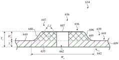
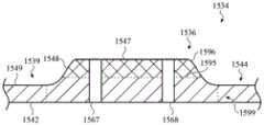
图6示出了电子设备的示例性构件634的局部横截面视图。在一些情况下,构件(另选地,覆盖构件)634为具有两个玻璃部件的玻璃构件,每个玻璃部件由玻璃层形成。图6中示出了构件634,其中构件634的外部表面644面朝上。该取向相对于图2至图5的视图旋转。构件634可为图1B的构件134或本文所述的任何其他构件或覆盖构件的示例。FIG. 6 shows a partial cross-sectional view of an
如图6所示,构件634包括第一部件699和第二部件696。第一部件诸如第一部件699在本文中也可被称为第一部分或第一组成。第二部件诸如第二部件696在本文中也可被称为第二部分或第二组成。第一部件699位于第二部件696下方,并且第二部件696通常具有比第一部件699的侧向尺寸小的至少一个侧向尺寸。As shown in FIG. 6 ,
构件634可为玻璃构件,第一部件699可为第一玻璃部件,并且第二部件696可为第二玻璃部件。在附加情况下,构件634为复合构件。作为一个示例,第一部件699为第一玻璃部件,并且第二部件696为玻璃陶瓷部件或陶瓷部件(或反之亦然)。结合图11提供的玻璃陶瓷部件或陶瓷部件的描述大体适用于本文,并且为简明起见,此处不再重复。
第一部件699包括或限定构件634的部分639,在本文中也称为基部部分639。基部部分639限定外部表面644的基部区域649。第一部件699还包括突起特征部636下面的部分635。突起特征部636从基部部分639突起或相对于基部部分至少部分地偏置。构件的突起特征部诸如突起特征部636在本文中也可统称为特征部。The
构件的第二部件696可至少部分地限定构件634的突起特征部636。在图6的示例中,第二部件696完全限定突起特征部636。然而,在其他示例中,第二部件696可部分地限定突起特征部,如图7至图9所示。突起特征部636限定外部表面644的凸起区域647。凸起区域647还限定图6中的突起特征部的顶部表面。凸起区域647可限定平台(基本上平面的表面区域)。在图6的示例中,外部表面的凸起区域647从外部表面644的基部区域649偏置距离H1。突起特征部636还限定宽度W6和侧面区域648,该侧面区域在外部表面644的凸起区域647和基部区域649之间延伸。The
虚线695示意性地指示第一部件699与第二部件696之间的边界区域。第一部件699可粘结到第二部件696,并且边界区域可接合该两个部件。在一些情况下,诸如当第一部件699为第一玻璃部件并且第二部件696为第二玻璃部件时,第一部件699可被熔合到第二部件696。在此类情况下,第一部件699和第二部件696可被称为熔合粘结的。当第一部件699被熔合到第二部件696时,边界区域在本文中也可称为熔合区。在一些实施方案中,第一部件699与第二部件696之间的熔合为基本上完全的。例如,第一部件699与第二部件696之间的边界或熔合区可包括极少(如果有的话)空隙,并且存在的任何空隙可相对于第一部件和第二部件的厚度为小的。在其他情况下,可使用中间材料诸如无机材料或有机材料(例如,粘合剂)将第一部件699粘结到第二部件696。中间材料相对于第一部件和第二部件可为薄的。Dashed
构件636的第一部件699可由第一玻璃层形成,并且构件的第二部件696可由第二玻璃层形成。虚线695可对应于第一玻璃层与第二玻璃层之间的边界。在一些情况下,可在第一部件699与第二部件696之间观察到不同的边界区域。在其他情况下,第一部件699与第二部件696之间的不同的边界区域不能通过肉眼来检测。The
例如,当第一玻璃层具有基本上类似于第二玻璃层的组合物并且第一玻璃部件与第二玻璃部件之间的熔合为基本上完全的时,不同的熔合区不能通过肉眼来检测。在一些情况下,可在熔合区中检测一个或多个熔合伪影,例如不完全熔合的区、空隙、石墨或由热成形工艺产生的其他杂质颗粒等。任何熔合伪影的尺寸可足够小,使得玻璃构件具有期望强度。例如,熔合伪影的尺寸可小于50微米、小于25微米、小于10微米或小于5微米。在一些情况下,可通过分割构件634和/或使用非破坏性技术来观察边界区域和/或熔合伪影。用于观察边界区域和/或熔合伪影的合适技术包括但不限于显微镜法、元素分析、光学干涉检测、超声检测等。For example, when the first glass layer has a composition substantially similar to that of the second glass layer and the fusion between the first glass part and the second glass part is substantially complete, the different fused regions cannot be detected by eye. In some cases, one or more fusion artifacts may be detected in the fusion zone, such as areas of incomplete fusion, voids, graphite or other foreign particles resulting from the thermoforming process, and the like. The size of any fusion artifacts may be small enough that the glass member has the desired strength. For example, the size of the fusion artifact may be less than 50 microns, less than 25 microns, less than 10 microns, or less than 5 microns. In some cases, border regions and/or fusion artifacts may be observed by segmenting
如图6所示,构件634还限定通孔,诸如通孔662。通孔662延伸穿过构件634的突起特征部636和下面部分635。构件634的第一部件可限定通孔662的下部部分或第一部分,并且构件的第二部件可限定通孔662的上部部分或第二部分。As shown in FIG. 6 ,
通孔662可允许输入到设备部件(诸如先前结合图1B和图2至图4所述的光学模块)、从该设备部件输出或者布置该设备部件。突起特征部636还可限定到通孔的开口667,其中开口667位于凸起区域647中。在一些情况下,构件634可限定布置结构、阵列、或延伸穿过突起特征部636的一组通孔和开口。例如,构件634可限定任何数量的通孔和开口,诸如一个、两个、三个、四个或五个通孔和开口。在附加实施方案中,构件不需要限定通孔,而是可以限定用于下面光学模块的窗口,如图9的示例所
如图6所示,外部表面644的凸起区域647包括纹理化区域656。除了开口诸如开口667之外,纹理化区域656可跨基本上整个凸起区域647延伸。例如,纹理化区域656可基本上跨由凸起区域647限定的平台延伸。在一些情况下,纹理化区域656可被限制于平台,而在附加情况下,纹理化区域656可跨外部表面的侧面区域648延伸。如果构件634要为均匀纹理化的,则纹理化区域656也可跨基部区域649延伸。As shown in FIG. 6 , raised
在一些情况下,基部区域649和凸起区域647两者均可限定外部表面644的相应纹理化区域(在本文中也称为纹理化表面区域)。例如,凸起区域647可限定第一纹理,并且基部区域649可限定不同于第一纹理的第二纹理。在一些情况下,侧面区域648(其也可称为周边区域)可限定第三纹理。例如,第三纹理可与第一纹理或第二纹理相同,或者可由第一纹理和第二纹理重叠而形成。如本文所用,纹理可包括相对平滑的纹理,诸如由抛光工艺产生的纹理。In some cases, both
如图6示意性地所示,(凸起区域647的)纹理化区域656的纹理可比基部区域649的纹理粗糙。例如,纹理化区域656可具有至少一个粗糙度参数,诸如均方根表面高度、均方根斜率和/或平均峰部曲率,该至少一个粗糙度参数大于基部区域649的粗糙度参数。在一些情况下,基部区域649可不包括纹理化区域或者可具有在触觉上和/或视觉上不同于纹理化区域656的纹理的平滑纹理。例如,基部区域649可具有由抛光工艺或玻璃成形工艺产生的相对平滑的纹理,诸如与抛光表面的纹理相对应的纹理。在一些情况下,凸起区域647的纹理化区域656可被配置为产生比开口667中的光学模块的窗口(例如,图2的窗口287)或透镜的光泽度水平更低的光泽度水平。纹理化区域656还可被配置为产生半透明外观和/或模糊外观。As schematically shown in FIG. 6 , the texture of the textured region 656 (of the raised region 647 ) may be coarser than the texture of the
在其他情况下,纹理化区域656的纹理可比基部区域649的纹理平滑。图4和图7示出了这种布置结构的示例。例如,纹理化区域656可具有与抛光表面的纹理类似的纹理,并且基部区域649可具有更粗糙的纹理。In other cases, the texture of
在图6的示例中,外部表面的凸起区域647从外部表面的基部区域649偏置距离H1。厚度T2(内部表面642与凸起区域647之间的距离)大于厚度T1(内部表面642与外部表面的基部区域649之间的距离)。例如,比率T2/T1可为约1.25至约3或约1.5至约2。在一些情况下,突起特征部636具有大于约1mm且小于或等于约2.5mm的厚度,并且基部部分639具有大于约0.5mm且小于约1mm的厚度。In the example of FIG. 6 , the raised
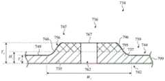
图7示出了电子设备的另一示例性构件734的局部横截面视图。构件(另选地,覆盖构件)734可包括两个部件799和796。在成形操作之后,两个部件之间的边界区域795可相对于外部表面744的基部区域749升高。在一些情况下,构件734为包括两个玻璃部件的玻璃构件,每个玻璃部件由玻璃层形成。图7中示出了构件734,其中构件734的外部表面744面朝上。构件734可为图1B的构件134的示例。构件734限定外部表面744、内部表面742、突起特征部736和基部部分739。突起特征部限定宽度W7。FIG. 7 shows a partial cross-sectional view of another
如图7所示,构件734包括第一部件799和第二部件796。第一部件799包括基部部分739、突起特征部736下面的部分735、以及限定突起特征部736的下部零件或第一零件的部分(另选地,零件)737。第二部件796限定突起特征部的上部零件或第二零件和外部表面的凸起区域747。第一部件799的区域737可限定侧表面748的下部零件或第一零件(另选地,部分),并且第二部件796可限定侧表面748的上部零件或第二零件(另选地,部分)。以如针对图6所述的类似方式,凸起区域747可限定平台,并且可从外部表面的基部区域749向外偏置。As shown in FIG. 7 ,
在图7的示例中,虚线795示意性地指示第一部件799与第二部件796之间的边界。在图7的示例中,边界从外部表面744的基部区域749的高度偏置,并且从内部表面742偏置大于厚度T3的距离H7。在一些情况下,诸如当第一部件和第二部件为玻璃部件时,第一部件799熔合粘结到第二部件796。如先前结合图6所述,第一部件799与第二部件796之间的熔合可为基本上完全的,或者一些小的不完全熔合区域可沿着边界存在。在其他示例中,可使用中间材料诸如无机材料或有机材料(例如,粘合剂)将第一部件799耦接到第二部件796,如先前结合图6所述。In the example of FIG. 7 , dashed
在一些情况下,第一部件799可以是由第一玻璃层形成的第一玻璃部件,并且第二部件796可以是由第二玻璃层形成的第二玻璃部件。虚线795可对应于第一玻璃层与第二玻璃层之间的边界。在附加情况下,构件734为复合构件。作为一个示例,第一部件799为第一玻璃部件,并且第二部件796为玻璃陶瓷部件或陶瓷部件(或反之亦然)。结合图11提供的玻璃陶瓷部件或陶瓷部件的描述大体适用于本文,并且为简明起见,此处不再重复。In some cases,
在一些情况下,在第一层耦接到第二层之后的层的成形(例如,机加工)导致层之间的边界从外部表面744的基部区域749的高度偏置,如结合图11和图12A至图12C更详细地描述。结合图11和图12A至图12C提供的描述大体适用于本文,并且为简明起见,此处不再重复。在一些示例中,第一部件799与第二部件796之间的不同的边界区域可能不容易通过肉眼来检测,而在其他示例中,边界区域或熔合伪影的至少一部分可通过肉眼或使用先前结合图6所讨论的其他技术来检测。结合图6提供的描述大体适用于本文,并且为简明起见,此处不再重复。In some cases, shaping (e.g., machining) of the layers after the first layer is coupled to the second layer results in the boundary between the layers being offset from the height of the
如图7所示,构件734还限定通孔,诸如通孔762。通孔762延伸穿过构件734的突起特征部736和下面部分735。构件734的第一部件799可限定通孔762的下部部分或第一部分,并且构件的第二部件796可限定通孔762的上部部分或第二部分。第二部件796还可限定到通孔的开口767,其中开口767位于凸起区域747中。通孔的布置结构和功能可如先前结合图6所述,并且为简洁起见,此处不再重复该描述。As shown in FIG. 7 ,
如图7所示,纹理化区域756跨外部表面744的基部区域749和侧表面748延伸。在图7的示例中,纹理化区域756的纹理可比凸起区域747的纹理粗糙。例如,凸起区域747可具有抛光纹理。然而,应当理解,该示例不是限制性的,并且纹理化区域756的纹理可为本文所述的纹理中的任一种纹理,包括结合图6所述的那些纹理。厚度T4(内部表面742与凸起区域747之间的距离)大于厚度T3(内部表面742与外部表面的基部区域749之间的距离)。这些厚度(T3和T4)的值和比率可如先前针对图6的厚度T1和T2所述,并且为简洁起见,此处不再重复。As shown in FIG. 7 ,
图8示出了电子设备的构件834的附加示例的局部横截面视图。在图8的示例中,构件(另选地,覆盖构件)834保持层状结构,并且可在层之间检测到不同的边界。在一些情况下,构件834由两个玻璃层形成,并且可在由两个玻璃层形成的两个玻璃部件之间检测到不同的边界895。图8中示出了构件834,其中构件834的外部表面844面朝上。构件834可为图1B的构件134的示例。构件834限定外部表面844、内部表面842、突起特征部836和基部部分839。突起特征部限定宽度W8。FIG. 8 shows a partial cross-sectional view of additional examples of
构件834包括第一部件899和第二部件896。在一些情况下,第一部件899可以是由第一玻璃层形成的第一玻璃部件,并且构件的第二部件896可以是由第二玻璃层形成的第二玻璃部件。在附加情况下,构件834为复合构件。作为一个示例,第一部件899为第一玻璃部件,并且第二部件896为玻璃陶瓷部件或陶瓷部件(或反之亦然)。结合图11提供的玻璃陶瓷部件或陶瓷部件的描述大体适用于本文,并且为简明起见,此处不再重复。
第一部件899包括基部部分839、突起特征部836下面的部分835、以及限定突起特征部836的下部零件或第一零件的部分(另选地,零件)837。第二部件896限定突起特征部836的上部零件或第二零件和外部表面的凸起区域847。第一部件899的区域837可限定侧表面848的下部零件或第一零件,并且第二部件896可限定侧表面848的上部零件或第二零件。以如针对图6所述的类似方式,凸起区域847可限定平台,并且可从外部表面的基部区域849向外偏置。The
在图8的示例中,第一部件899粘结到第二部件896。线895示意性地指示第一部件899与第二部件896之间的边界。在图8的示例中,由线895指示的边界是不同的并且跨突起特征部836延伸。在一些情况下,线895指示熔合区。该边界从外部表面844的基部区域849的高度偏置,并且从内部表面842偏置大于厚度T5的距离H8。在其他示例中,可使用中间材料诸如无机材料或有机材料(例如,粘合剂)将第一部件899耦接到第二部件896,如先前结合图6所述。In the example of FIG. 8 ,
在一些情况下,构件834的第一部件899可由第一玻璃层形成,并且构件的第二部件896可由第二玻璃层形成。实线895可对应于第一玻璃层与第二玻璃层之间的边界区域,该边界区域可通过肉眼跨突起特征部来检测。如先前结合图7所述,在第一玻璃层耦接到第二玻璃层之后的构件836的机加工导致层之间的边界区域从基部区域849的高度偏置。结合图11和图12A至图12C提供的描述大体适用于本文,并且为简明起见,此处不再重复。In some cases,
如图8所示,构件834还限定通孔,诸如通孔862。通孔862延伸穿过构件834的突起特征部836和下面部分835。构件834的第一部件899可限定通孔862的下部部分或第一部分,并且构件的第二部件896可限定通孔862的上部部分或第二部分。As shown in FIG. 8 ,
通孔862可允许输入到设备部件(诸如先前结合图1B和图2至图4所述的光学模块)、从该设备部件输出或者布置该设备部件。突起特征部836还可限定到通孔的开口867,其中开口867位于凸起区域847中。通孔的布置结构和功能可如先前结合图6所述,并且为简洁起见,此处不再重复该描述。
如图8所示,外部表面844的凸起区域847包括纹理化区域856。在图8的示例中,纹理化区域856的纹理可比基部区域849的纹理粗糙。然而,应当理解,该示例不是限制性的,并且纹理化区域856的纹理可为本文所述的纹理中的任一种纹理,包括结合图6所述的那些纹理。此外,厚度T6(内部表面842与凸起区域847之间的距离)大于厚度T5(内部表面842与外部表面的基部区域849之间的距离)。这些厚度(T5和T6)的值和比率可如先前针对图6的厚度T1和T2所述,并且为简洁起见,此处不再重复。As shown in FIG. 8 , raised
图9示出了电子设备的构件934的另外的示例的局部横截面视图。构件(另选地,覆盖构件)934可由三层(例如,三个玻璃层)形成,以便在孔962上方提供“窗口”。图9中示出了构件934,其中构件934的外部表面944面朝上。构件934可为图1B的构件134的示例。构件934限定外部表面944、内部表面942、突起特征部936和基部部分939。突起特征部限定宽度W9。FIG. 9 shows a partial cross-sectional view of another example of a
如图9所示,构件934包括第一部件999、第二部件996和第三部件997。在一些情况下,构件934为玻璃构件,第一部件999为第一玻璃部件,第二部件996为第二玻璃部件,并且第三部件997为第三玻璃部件。在附加情况下,构件934为复合构件。作为一个示例,第一部件999为第一玻璃部件,第二部件996为第二玻璃部件,并且第三部件997为玻璃陶瓷部件或陶瓷部件。限定第三部件的玻璃材料、玻璃陶瓷材料或陶瓷材料对可见光、红外线辐射、紫外线辐射或它们的组合可以是透明的。结合图11提供的玻璃陶瓷部件或陶瓷部件的描述大体适用于本文,并且为简明起见,此处不再重复。As shown in FIG. 9 ,
第一部件999包括基部部分939、突起特征部936下面的部分935、以及限定突起特征部936的下部零件或第一零件的部分(另选地,零件)937。第二部件996限定突起特征部的中间零件或第二零件。第三部件997限定突起特征部的上部零件或第三零件和外部表面的凸起区域947。第一部件999的部分937可限定侧表面948的下部零件或第一零件,第二部件996可限定侧表面948的中间零件或第二零件,并且第三部件997可限定侧表面948的上部零件或第三零件。以如针对图6所述的类似方式,凸起区域947可限定平台,并且可从外部表面的基部区域949向外偏置。The
虚线995a和虚线995b示意性地指示第一部件999、第二部件996与第三部件997之间的边界。在图9的示例中,边界995a和边界995b从外部表面944的基部区域949的高度偏置,并且分别从内部表面942偏置距离H9和H10(各自大于厚度T7)。在一些情况下,诸如当第一部件、第二部件和第三部件为玻璃部件时,第一部件999熔合粘结到第二部件996并且第二部件996熔合粘结到第三部件997。如先前结合图6所述,第一部件999与第二部件996之间以及第二部件996与第三部件997之间的熔合可为基本上完全的,或者一些小的不完全熔合区域可沿着边界存在。在其他示例中,第一部件、第二部件和第三部件可使用中间材料诸如无机材料或有机材料(例如,粘合剂)来耦接,如先前结合图6所述。
构件934的第一部件999可由第一玻璃层形成,构件的第二部件996可由第二玻璃层形成,并且构件的第三部件997可由第三玻璃层形成。在一些情况下,在熔合玻璃层之前在第二玻璃层中形成一个或多个孔以便有利于孔962的形成。虚线995a和虚线995b可对应于玻璃层之间的边界区域。在一些示例中,第一部件999与第二部件996和/或第二部件996与第三部件997之间的不同的边界区域不能通过肉眼来检测,而在其他示例中,一个或多个边界区域的至少一部分或熔合伪影可通过肉眼或使用先前结合图6所讨论的其他技术来检测。结合图6提供的描述大体适用于本文,并且为简明起见,此处不再重复。The
如图9所示,构件934还限定孔,诸如孔962。孔962延伸穿过第二部件996以及第一部件999的下面部分935,但不延伸穿过第三部件997。孔962也可称为盲孔。因此,第三部件997可在孔962上方提供窗口。构件934的第一部件999可限定孔962的下部部分或第一部分,并且构件的第二部件996可限定孔962的上部部分或第二部分。孔962可允许输入到设备部件(诸如先前结合图1B和图2至图4所述的光学模块)、从该设备部件输出或者布置该设备部件。玻璃构件的第三部件997可用作光学模块的窗口。孔的数量可以类似于先前结合图6所述的通孔的数量,并且为简洁起见,此处不再重复描述。As shown in FIG. 9 ,
如图9所示,外部表面944包括纹理化区域956。在图9的示例中,纹理化区域的纹理跨凸起区域947、侧表面948和基部区域延伸。例如,纹理化区域956可具有抛光纹理。在附加示例中,纹理化区域956的纹理可以比基部区域949的纹理平滑,以有利于其用作光学部件的窗口。厚度T8(内部表面942与凸起区域947之间的距离)大于厚度T7(内部表面942与外部表面的基部区域949之间的距离)。这些厚度(T7和T8)的值和比率可如先前针对图6的厚度T1和T2所述,并且为简洁起见,此处不再重复。As shown in FIG. 9 , exterior surface 944 includes
图10示出了构件1034的纹理化区域1056的详细视图。纹理化区域1056可为图6的细节区域1-1中的纹理化区域656的示例或本文所示的任何其他纹理化区域的示例。在一些情况下,纹理化区域1056可由构件1034的外部表面1047的凸起区域限定,如先前结合图6所述。纹理化区域在本文中也可称为纹理化表面区域。FIG. 10 shows a detailed view of
纹理化区域1056包括多个表面特征部1080。图10中提供的表面特征部1080的示例不是限制性的,并且一般来讲,构件1034的表面区域的表面特征部1080可限定一系列形状或配置中的任一种。表面特征部1080可具有多种形状,诸如圆化特征部或角特征部。例如,表面特征部1080可限定圆形、椭圆形、多边形、矩形或不规则表面轮廓。此外,表面特征部1080可限定突起部、凹陷部或它们的组合,并且可具有任何合适的形状,可为金字塔形、锥形、圆柱形、拱形,且具有弯曲上表面或截头形状诸如圆锥等。
如图10所示,表面特征部1080可限定一个或多个凹陷部,诸如表面特征部1084。凹陷部可限定最低点,诸如点1085。表面特征部1080还可限定一个或多个突起部,诸如表面特征部1086。突起部可限定最高点,诸如点1087。如图10示意性地所示,表面特征部1080可限定一组最低点和一组最高点。该组最高点也可称为一组峰部。表面特征部1080可限定一组凹陷部,每个凹陷部定位在该组峰部的相邻峰部之间。峰部和谷部的形状不限于图10示意性地所示的那些形状。例如,峰部中的至少一些可具有稍微较大的曲率半径(和较小的曲率半径),以除了提供纹理化表面期望水平的可清洁度之外还提供期望的触觉特性。As shown in FIG. 10 ,
在一些实施方案中,表面特征部1080限定一组山部和谷部。可使用如下文所述的平面纹理分析技术来限定山部和谷部。表面特征部1086可大体对应于山特征部,并且表面特征部1084可大体对应于谷特征部。在一些实施方案中,一组山部和谷部在山特征部、谷特征部或它们的组合之间具有基本上均匀的间距。在附加实施方案中,一组谷部可在山特征部和/或谷特征部之间具有不均匀或不规则的间距。In some embodiments, surface features 1080 define a set of hills and valleys. The hills and valleys may be defined using planar texture analysis techniques as described below. Surface features 1086 may generally correspond to mountain features, and surface features 1084 may generally correspond to valley features. In some embodiments, a set of hills and valleys has a substantially uniform spacing between hill features, valley features, or combinations thereof. In additional embodiments, a set of valleys may have uneven or irregular spacing between mountain features and/or valley features.
表面特征部1080的高度可相对于参考表面1082来测量。例如,山部的高度可根据最高点(例如,点1087)来确定,并且谷部的高度可根据最低点(例如,点1085)来确定。构件1034可为构件134或本文所述的任何其他构件的示例。这些构件的细节适用于构件1034,并且为简明起见,此处将不再重复。The height of
表面特征部1080可被配置为向构件1034的一个或多个表面区域以及向包括构件1034的覆盖组件和电子设备提供特定光学特性。然而,限定表面区域的纹理的表面特征部1080可为不可单独视觉感知的。在一些情况下,表面区域的纹理可使得构件1034看起来是半透明的,而不是透明的。在一些情况下,纹理可被配置为提供特定水平的此类光学特性,诸如透射雾度、清晰度、光泽度、粒度以及它们的组合。Surface features 1080 may be configured to provide particular optical properties to one or more surface regions of
构件的纹理化表面区域诸如纹理化区域1056可被配置为向表面提供指定的光泽度水平。在一些实施方案中,在60度下测量时,纹理化区域1056可具有小于约50光泽度单位、小于约40光泽度单位、2光泽度单位至20光泽度单位、2光泽度单位至10光泽度单位、5光泽度单位至50光泽度单位、5光泽度单位至20光泽度单位、10光泽度单位至50光泽度单位、10光泽度单位至45光泽度单位、或15光泽度单位至45光泽度单位的光泽度值。可在不存在美观涂层时测量光泽度水平。在附加实施方案中,纹理化区域1056可具有较高光泽度。例如,具有相对高光泽度的纹理化区域1056可具有大于约70光泽度单位且小于或等于约150光泽度单位的光泽度值。在一些情况下,纹理化区域的光泽度和外部表面的另一个区域的光泽度之间的差值可为至少10%并且可大于100%。在一些情况下,纹理化区域的光泽度可使用可商购获得的装置并且根据ASTM或ISO标准测试方法来测量。角度测量可指入射光与表面纹理化区域的垂线之间的角度。A textured surface area of a component, such as
构件1034的纹理化表面区域诸如纹理化区域1056可被配置为向构件的对应部分提供指定水平的透射雾度。在一些情况下,纹理化区域的透射雾度可使用可商购获得的装置并且根据ASTM或ISO标准测试方法来测量。透射雾度可与受到广角散射(例如,大于2.5度)的光的量有关。在一些情况下,透射雾度可大于或等于约50%、大于或等于约60%、或大于或等于约70%。例如,透射雾度可为约60%至约90%、或约70%至约80%。作为非限制性示例,透射雾度可使用购自BYK的haze-gard i设备或购自Nippon Denshoku的GC 5000L可变光度计来测量。当覆盖组件或构件从电子设备移除时,可测量该覆盖组件或构件的透射雾度散射。构件的外部表面的另一个区域诸如基部区域的透射雾度可类似于或不同于纹理化区域1056的透射雾度。A textured surface region of
构件1034的纹理化表面区域诸如纹理化区域1056可被配置为向构件的对应部分提供指定水平的清晰度。纹理化区域的清晰度或透射窄角散射可使用可商购获得的装置并且根据ASTM或ISO标准测试方法来测量。在一些情况下,清晰度可为小于约50%、小于约40%、小于约30%、小于约20%、小于约15%、或小于约10%。例如,清晰度可为约5%至约30%、约5%至约20%、约5%至约15%、或约5%至约15%。透射窄角散射可使用购自BYK的haze-gard i设备或购自Nippon Denshoku的GC 5000L可变光度计来测量。可根据中心区域中的强度(I中心)和围绕中心区域的环中的强度(I环)的测量结果来确定清晰度值。例如,清晰度值可等于100%*(I中心-I环)/(I中心+I环)。当覆盖组件或构件从电子设备移除时,可测量该覆盖组件或构件的清晰度或透射窄角散射。A textured surface region of
在一些情况下,构件的纹理化区域可被配置为向构件的对应部分提供指定水平的视觉均匀度。构件的外部表面的另一个区域诸如基部区域的视觉均匀度水平可类似于或不同于纹理化区域1056的视觉均匀度水平。纹理化区域的粒度可使用可商购获得的装置在漫射照明下测量。可类似地测量覆盖组件的纹理化区域的粒度。在一些情况下,构件1034的纹理化表面的图像可使用数字相机获得,并且可确定该图像的每个像素的亮度,从而允许确定在纹理化表面上的亮度变化。例如,购自BYK的BYK-mac设备可产生根据亮度水平的柱状图来确定的粒度值。纹理化表面的粒度可小于约1.5或小于约1.0。此外,粒度可为约0.1至约1.5、约0.1至约1.0、约0.25至约1.5、约0.25至约1.0、约0.5至约1.5、或约0.5至约1.0。可在向构件施加任何美观涂层之前测量这些粒度值。In some cases, a textured region of a component may be configured to provide a specified level of visual uniformity to a corresponding portion of the component. Another region of the exterior surface of the component, such as the base region, may have a level of visual uniformity similar to or different than the level of visual uniformity of
构件1034的纹理化表面区域诸如纹理化区域1056可被配置为提供指定水平的可清洁度。例如,纹理化区域1056的纹理可被配置为使得特征部的均方根(RMS)高度不会过大。纹理还可被配置为使得任何凹面特征部的尺寸足够大以有利于清洁。此外,纹理可被配置为使得表面特征部的均方根(RMS)斜率和/或平均峰部曲率足够小,以除了提供期望水平的可清洁度之外还提供期望的触觉特性。Textured surface regions of
表面纹理参数包括平面表面纹理参数,诸如幅值参数、空间参数和混合参数。表面过滤可用于在确定表面纹理参数之前排除表面噪波和/或表面波度。此外,分割技术可用于确定特征部参数,诸如最大直径、最小直径、面积和周长。这些参数可根据投影到参考表面(例如,参考平面)上的特征部形状来计算。可为给定类别的表面特征部(例如,山部或谷部)确定平均值。表面纹理参数和用于确定这些参数的方法(包括过滤和分割)更详细描述于国际标准化组织(ISO)标准25178(产品几何技术规范(GPS)—表面纹理:平面)中。Surface texture parameters include planar surface texture parameters such as magnitude parameters, spatial parameters, and blend parameters. Surface filtering can be used to exclude surface noise and/or surface waviness before determining surface texture parameters. Additionally, segmentation techniques can be used to determine feature parameters such as maximum diameter, minimum diameter, area, and perimeter. These parameters can be calculated from the feature shape projected onto a reference surface (eg, a reference plane). Average values may be determined for a given class of surface features (eg, hills or valleys). Surface texture parameters and methods for determining these parameters, including filtering and segmentation, are described in more detail in International Organization for Standardization (ISO) standard 25178 (Geometric Product Specification (GPS) - Surface Texture: Planar).
这些表面纹理参数可使用可商购获得的装置(包括使用光学测量技术的装置)来测量。示例性光学测量技术是干涉测量法,并且使用该技术的商购装置的示例是相干扫描干涉测量轮廓仪(白光),诸如Zygo相干扫描干涉测量光学轮廓仪。另一示例性光学测量技术是共焦显微镜法,并且使用该技术的商购装置的示例是激光扫描共焦显微镜,诸如Keyence激光扫描共焦显微镜。图像可被平铺以测量较大面积。These surface texture parameters can be measured using commercially available devices, including devices using optical measurement techniques. An exemplary optical measurement technique is interferometry, and an example of a commercially available device using this technique is a coherent scanning interferometric profiler (white light), such as a Zygo coherent scanning interferometric optical profiler. Another exemplary optical measurement technique is confocal microscopy, and an example of a commercially available device using this technique is a laser scanning confocal microscope, such as a Keyence laser scanning confocal microscope. Images can be tiled to measure larger areas.
例如,构件1034的一个或多个表面区域的表面特征部1080可部分地通过表面特征部的高度来表征。该高度可相对于参考表面(由图10中的线1082示意性地示出)(诸如该表面的算术平均值)来测量。表面特征部1080的高度可能不均匀,使得表面特征部具有高度的分布。表面特征部1080的高度的量值可落在零至约5微米、零至约2.5微米、零至约2微米、零至约1.5微米、或零至约1微米的范围内。表面特征部1080可通过表面的均方根高度Sq或算术平均高度Sa来表征。表面特征部1080的均方根(RMS)高度可为大于零且小于约5微米、大于零且小于约2.5微米、大于零且小于约2微米、大于零且小于约1.5微米、大于零且小于约1微米、约0.1微米至约2.5微米、约0.1微米至约2微米、约0.1微米至约1.5微米、约0.1微米至约1.25微米、约0.1微米至约1.0微米、约0.2微米至约2.5微米、约0.2微米至约2微米、约0.2微米至约1.5微米、约0.2微米至约1.25微米、约0.2微米至约1.0微米、约0.25微米至约2.5微米、约0.25微米至约2微米、约0.25微米至约1.5微米、约0.25微米至约1.25微米、约0.25微米至约1.0微米、约0.5微米至约2.5微米、约0.5微米至约2微米、约0.5微米至约1.5微米、约0.5微米至约1.25微米、约0.5微米至约1.0微米、约0.75微米至约5微米、或约1微米至约5微米。在一些情况下,当一个纹理化区域具有较大的RMS高度时,其可被称为比另一个纹理化区域粗糙。For example, surface features 1080 of one or more surface regions of
构件1034的外部表面的另一个区域诸如基部区域的RMS高度可类似于或不同于纹理化区域1056的RMS高度。例如,凸起区域的RMS高度可大于基部区域的RMS高度。例如,凸起区域的RMS高度可比基部区域的RMS高度大至少10%且小于150%、至少10%且小于100%、或至少10%且小于50%。在一些情况下,基部区域的RMS高度可小于0.5微米、小于250nm、或1nm至约250nm。在一些情况下,基部区域的RMS高度可类似于抛光表面的RMS高度,诸如约1nm至约150nm、约1nm至约125nm、约1nm至约100nm、约1nm至约75nm、约1nm至约50nm、约1nm至约25nm、或约1nm至约10nm。Another region of the exterior surface of
此外,该一个或多个表面区域的表面特征部1080可通过侧向参数诸如峰部之间的距离来表征。峰部之间的间距可能不均匀,使得在峰部之间存在间距的分布。峰部之间的平均距离或间距可称为平均节距。平均节距可为约1微米至约20微米、约1微米至约15微米、约1微米至约10微米、约2.5微米至约20微米、约2.5微米至约15微米、约2.5微米至约10微米、约5微米至约40微米、约5微米至约20微米、约5微米至约15微米、或约5微米至约10微米。Additionally, the surface features 1080 of the one or more surface regions can be characterized by lateral parameters such as distances between peaks. The spacing between peaks may not be uniform such that there is a distribution of spacing between the peaks. The average distance or spacing between peaks may be referred to as the average pitch. The average pitch can be from about 1 micron to about 20 microns, from about 1 micron to about 15 microns, from about 1 micron to about 10 microns, from about 2.5 microns to about 20 microns, from about 2.5 microns to about 15 microns, from about 2.5 microns to about 10 microns, about 5 microns to about 40 microns, about 5 microns to about 20 microns, about 5 microns to about 15 microns, or about 5 microns to about 10 microns.
在一些实施方案中,该一个或多个表面区域的表面特征部1080可被配置为具有峰部的平均高度与峰部的平均间距的特定比率。例如,RMS高度与平均节距的比率可为约0.01至约0.6、约0.01至约0.3、约0.02至约0.6、约0.02至约0.3、约0.03至约0.6、约0.03至约0.3、约0.04至约0.6、或约0.04至约0.3。In some embodiments, the surface features 1080 of the one or more surface regions can be configured to have a particular ratio of the average height of the peaks to the average spacing of the peaks. For example, the ratio of RMS height to average pitch can be about 0.01 to about 0.6, about 0.01 to about 0.3, about 0.02 to about 0.6, about 0.02 to about 0.3, about 0.03 to about 0.6, about 0.03 to about 0.3, about 0.04 to about 0.6, or about 0.04 to about 0.3.
该一个或多个表面区域的表面特征部1080还可通过侧向尺寸来表征。例如,表面特征部1080可通过最大侧向(或线性)尺寸和最小侧向(或线性)尺寸来表征。表面特征部1080可具有足够小的最大侧向尺寸,使得这些表面特征部不可被视觉感知为单独的特征部。此外,表面特征部1080的侧向尺寸和间距可被配置为使得构件具有足够低水平的粒度。The surface features 1080 of the one or more surface regions can also be characterized by lateral dimensions. For example, surface features 1080 may be characterized by a maximum lateral (or linear) dimension and a minimum lateral (or linear) dimension. Surface features 1080 may have a maximum lateral dimension that is small enough that the surface features are not visually perceivable as separate features. Furthermore, the lateral dimensions and spacing of the surface features 1080 can be configured such that the components have a sufficiently low level of granularity.
该一个或多个表面区域的表面特征部1080可通过均方根斜率(Sdq)(也称为均方根梯度)来表征。在一些实施方案中,均方根斜率可为大于零且小于约1.25、大于零且小于约1、约0.1至小于约1.25、约0.1至小于约1、约0.25至小于约1、约0.25至约0.75、或约0.1至约0.5。在一些情况下,凸起区域的均方根斜率大于基部区域的均方根斜率。例如,凸起区域的均方根斜率可比基部区域的均方根斜率大至少10%且小于60%。The surface features 1080 of the one or more surface regions may be characterized by a root mean square slope (Sdq), also known as a root mean square gradient. In some embodiments, the root mean square slope can be greater than zero and less than about 1.25, greater than zero and less than about 1, about 0.1 to less than about 1.25, about 0.1 to less than about 1, about 0.25 to less than about 1, about 0.25 to about 0.75, or about 0.1 to about 0.5. In some cases, the root mean square slope of the raised region is greater than the root mean square slope of the base region. For example, the root mean square slope of the raised region may be at least 10% greater and less than 60% greater than the root mean square slope of the base region.
该一个或多个表面区域的表面特征部1080还可通过峰部(也称为峰顶点)的曲率来表征,诸如通过算术平均峰顶点曲率Ssc(在本文中也称为平均峰部曲率)来表征。在一些实施方案中,算术平均峰顶点曲率为大于零且小于约2.0微米、大于零且小于或等于约1.5微米-1、约0.1微米-1至约2.0微米-1、约0.1微米-1至约1.5微米-1、约0.25微米-1至约2.0微米-1、约0.25微米-1至约1.5微米-1、约0.5微米-1至约2.0微米-1、约0.5微米-1至约1.5微米-1、约0.75微米-1至约2.0微米-1、约0.75微米-1至约1.5微米-1。在一些情况下,凸起区域的平均峰部曲率大于基部区域的平均峰部曲率。例如,凸起区域的平均峰部曲率可比基部区域的平均峰部曲率大至少10%且小于50%。The surface features 1080 of the one or more surface regions may also be characterized by the curvature of the peak (also referred to as the peak apex), such as by the arithmetic mean peak apex curvature Ssc (also referred to herein as the mean peak curvature) to represent. In some embodiments, the arithmetic mean peak apex curvature is greater than zero and less than about 2.0 microns, greater than zero and less than or equal to about 1.5 microns-1 , about 0.1 microns-1 to about 2.0 microns-1 , about 0.1 microns-1 to about 1.5 micron-1 , about 0.25 micron-1 to about 2.0 micron-1 , about 0.25 micron-1 to about 1.5 micron-1 , about 0.5 micron-1 to about 2.0 micron-1 , about 0.5 micron-1 to about 1.5 Micron-1 , about 0.75 micron-1 to about 2.0 micron-1 , about 0.75 micron-1 to about 1.5 micron-1 . In some cases, the average peak curvature of the raised regions is greater than the average peak curvature of the base region. For example, the average peak curvature of the raised regions can be at least 10% and less than 50% greater than the average peak curvature of the base region.
该一个或多个表面区域的表面特征部1080还可通过自相关长度来表征。在一些实施方案中,自相关长度为约1微米至约50微米、约2微米至约30微米、或约3微米至约25微米。The surface features 1080 of the one or more surface regions may also be characterized by autocorrelation lengths. In some embodiments, the autocorrelation length is from about 1 micron to about 50 microns, from about 2 microns to about 30 microns, or from about 3 microns to about 25 microns.
图11示出了用于由至少两个玻璃层形成玻璃构件的示例性过程1100的流程图。通常,玻璃构件和每个玻璃层包括基于二氧化硅的玻璃材料。玻璃材料可具有网络结构,诸如基于硅酸盐的网络结构。在一些实施方案中,玻璃材料包括硅铝酸盐玻璃。如本文所用,硅铝酸盐玻璃包括元素铝、硅和氧,但还可包括其他元素。通常,玻璃材料包括可离子交换的玻璃材料,诸如碱金属硅铝酸盐玻璃(例如,锂硅铝酸盐玻璃)。可离子交换的硅铝酸盐玻璃可包含一价离子或二价离子,这些一价离子或二价离子补偿由于铝离子替换硅离子而引起的电荷。合适的一价离子包括但不限于碱金属离子,诸如Li+、Na+或者K+。合适的二价离子包括碱土离子,诸如Ca2+或者Mg2+。结合图11提供的合适玻璃材料的描述大体适用于本文所述的构件(覆盖构件)和玻璃层。在一些情况下,每个玻璃层具有基本上类似的组合物。在附加情况下,玻璃层可在组合物上不同。FIG. 11 shows a flowchart of an
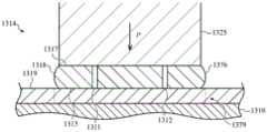
用于形成玻璃构件的玻璃层可在组装玻璃层的操作1110之前成形。玻璃层可通过机加工成形为期望形状和尺寸。此外,可对玻璃层的表面进行修整,使得相邻层可彼此紧密接触。在一些情况下,相邻玻璃层的表面为基本上平坦且平滑的,如图12A至图12C示意性地示出。在其他情况下,相邻玻璃层的表面中的一个表面是圆化的,而不是平坦的,如图14A和图15A示意性地示出。在一些情况下,可在玻璃层中的一个或多个玻璃层中形成(例如,通过机加工)导向孔,如图13A和图13B示意性地示出。The glass layers used to form the glass member may be shaped prior to
在成形操作之后,形成玻璃构件的第一部分或下部部分的玻璃层通常具有比形成玻璃构件的上部部分的玻璃层大的侧向尺寸。在一些情况下,形成玻璃构件的第一部分或下部部分的第一玻璃层的厚度为0.5mm至1mm或0.75mm至1.5mm,并且形成玻璃的上部部分的玻璃层的厚度为0.75mm至1.5mm或1.0mm至2mm。在一些情况下,玻璃层的期望形状包括圆角或倒角。在成形操作之后,可诸如通过洗涤来清洁玻璃层。还可以在成形操作之后对玻璃层进行蚀刻或等离子体处理。After the forming operation, the glass plies forming the first or lower portion of the glass member generally have larger lateral dimensions than the glass plies forming the upper portion of the glass member. In some cases, the first glass layer forming the first or lower portion of the glass member has a thickness of 0.5 mm to 1 mm or 0.75 mm to 1.5 mm, and the glass layer forming the upper portion of glass has a thickness of 0.75 mm to 1.5 mm or 1.0mm to 2mm. In some cases, the desired shape of the glass layer includes rounded or chamfered corners. After the forming operation, the glass plies can be cleaned, such as by washing. It is also possible to etch or plasma treat the glass layer after the shaping operation.
图11的过程1100包括组装用于形成玻璃构件的玻璃层的操作1110,从而形成玻璃层的组件(在本文中也称为组件)。在一些实施方案中,操作1110包括组装第一玻璃层与第二玻璃层以形成玻璃层的组件。在一些情况下,这些层可通过使它们彼此接触来组装。在附加情况下,这些层可在操作1110期间诸如通过激光粘结、光学粘结等至少部分地粘结。两个玻璃层的组件的示例在图12A、图13A、图14A和图15A中示出。组装操作可在清洁条件下执行,以限制外来物质在玻璃层之间的引入。
如图11所示,过程1100包括熔合(也称为熔合粘结)玻璃层的组件以形成熔合组件的操作1120。通常,熔合操作包括加热组件并向组件的至少上层施加压力。玻璃层的组件可在热成形装置中加热并施加压力,该热成形装置也可称为成形工具。在一些情况下,组件放置在支撑表面上,并且工具件诸如柱塞、活塞等接触组件的上层,如图12A和图13A示意性地示出。例如,支撑表面可为基本上平坦的。As shown in FIG. 11 ,
熔合操作可包括将玻璃层的组件加热到每个玻璃层的玻璃化转变温度与软化点之间的温度,加热到每个玻璃层的退火点与软化点之间的温度,或加热到每个玻璃层的应变点与软化点之间的温度。例如,应变点(粘度为约1014.5泊)是以小时为单位减轻玻璃内应力的温度。退火点(粘度为约1013.2泊至1013.4泊)是以分钟为单位减轻玻璃内应力的温度。膨胀软化点由约109泊至1011泊的粘度限定,而玻璃软化点由约107.6泊的粘度限定;如本文所指的“软化点”可指这些温度中的任一者。工作点由约104泊的粘度限定。玻璃化转变温度(粘度为约1012泊至1013泊)是玻璃从过冷液体转变为玻璃态的温度。加热可以若干阶段进行。在一些情况下,当工具件搁置在组件的上层上并且组件整体搁置在支撑表面上时,可加热组件。The fusing operation may include heating the assembly of glass layers to a temperature between the glass transition temperature and softening point of each glass layer, to a temperature between the annealing point and softening point of each glass layer, or to a temperature between each The temperature between the strain point and softening point of the glass layer. For example, the strain point (viscosity of about 1014.5 poise) is the temperature at which internal stresses in the glass are relieved in hours. The annealing point (viscosity of about 1013.2 poise to 1013.4 poise) is the temperature at which the internal stress of the glass is relieved in minutes. The dilatant softening point is defined by a viscosity of about 109 Poise to 1011 Poise, while the glass softening point is defined by a viscosity of about 107.6 Poise; "softening point" as referred to herein may refer to any of these temperatures. The operating point is defined by a viscosity of about 104 poise. The glass transition temperature (viscosity of about 1012 to 1013 poise) is the temperature at which glass transitions from a supercooled liquid to a glassy state. Heating can be performed in several stages. In some cases, the assembly may be heated while the tool piece rests on an upper layer of the assembly and the assembly as a whole rests on the support surface.
熔合操作还可包括向组件的至少上层施加压力。在一些情况下,工具件接触组件的上层,但不接触组件的其余部分,同时通过工具件向组件施加压力。在一些情况下,压力可大于由于工具件的重量而产生的压力。在一些情况下,组件的下层与上层之间的熔合可开始于上层的中心区域,然后可朝上层的侧面向外移动。图16A和图16B示意性地示出了此类熔合操作中熔合前端的移动。图14A和图15A示出了可在熔合操作期间导致熔合前端的此类移动的层形状的示例。The fusing operation may also include applying pressure to at least an upper layer of the assembly. In some cases, the tool piece contacts the upper layer of the assembly, but not the rest of the assembly, while applying pressure to the assembly through the tool piece. In some cases, the pressure may be greater than the pressure due to the weight of the tool piece. In some cases, the fusion between the lower and upper layers of the assembly may begin in the central region of the upper layer and then may move outward toward the sides of the upper layer. Figures 16A and 16B schematically illustrate the movement of the fusion front in such a fusion operation. Figures 14A and 15A show examples of layer shapes that may cause such movement of the fusion front during the fusing operation.
熔合玻璃层的组件的操作形成一体的熔合组件。由多个玻璃层形成的熔合组件的部分通常具有比由单个玻璃层形成的熔合组件的部分大的厚度。此外,熔合组件的该较厚部分从熔合组件的较薄部分的相邻部分突起。玻璃构件的突起特征部将位于该较厚部分内,而基部部分将位于相邻的较薄部分内。较厚部分和较薄部分中的每一者限定外部表面和内部表面。熔合玻璃层的组件的操作不需要实现层之间的完全熔合。例如,当在操作1130中要从熔合组件的上层的侧表面移除材料时,在操作1130中要移除的上层的一些材料不需要完全熔合到熔合组件的下层。The operation of fusing the assembly of glass layers forms a unitary fused assembly. Portions of the fused assembly formed from multiple glass layers typically have a greater thickness than portions of the fused assembly formed from a single glass layer. Furthermore, the thicker portion of the fused component protrudes from an adjacent portion of the thinner portion of the fused component. The raised feature of the glass member will be located within this thicker portion, while the base portion will be located within the adjacent thinner portion. Each of the thicker portion and the thinner portion defines an exterior surface and an interior surface. The operation of fusing the assembly of glass layers need not achieve complete fusion between the layers. For example, when material is to be removed from the side surfaces of the upper layer of the fused assembly in
在一些情况下,玻璃层之间的边界区域的至少一部分可在熔合玻璃层的操作之后通过肉眼或使用其他技术来检测。边界区域的至少一部分可被检测为例如不完全熔合区、石墨或源自热成形装置的另一种材料的颗粒、或两者。在一些情况下,可通过分割玻璃构件和/或使用非破坏性技术来观察边界区域。用于观察边界区域的合适技术包括但不限于显微镜法、元素分析、光学干涉检测、超声检测等。如本文所提及的,“玻璃构件”、“玻璃层”、“玻璃部件”和/或“玻璃件”可包含一些相对少量的杂质或结晶材料,诸如按构件的重量计1%或更少、2%或更少、或5%或更少。In some cases, at least a portion of the boundary region between the glass layers is detectable by eye or using other techniques after the operation of fusing the glass layers. At least a portion of the boundary region may be detected as, for example, an incompletely fused region, particles of graphite or another material originating from the thermoforming device, or both. In some cases, the boundary region may be observed by segmenting the glass member and/or using non-destructive techniques. Suitable techniques for viewing the boundary region include, but are not limited to, microscopy, elemental analysis, optical interferometry, ultrasonic testing, and the like. As referred to herein, a "glass component," "glass ply," "glass component" and/or "glass piece" may contain some relatively small amount of impurity or crystalline material, such as 1% or less by weight of the component , 2% or less, or 5% or less.
在其他情况下,熔合可以是充分完全的,使得在熔合组件的与组件的层对应的部分之间用肉眼不能检测到不同的边界区域。例如,当两个相邻的玻璃层具有类似的组合物并且这些玻璃层之间的熔合为基本上完全的时,用肉眼不能检测到不同的边界区域。In other cases, the fusion may be sufficiently complete such that no distinct boundary regions are visually detectable between portions of the fused assembly corresponding to the layers of the assembly. For example, when two adjacent glass plies have similar compositions and the fusion between the glass plies is substantially complete, the distinct border regions cannot be detected with the naked eye.
过程1100还可包括冷却熔合组件的操作。熔合组件的冷却可以是足够平缓的,使得热致残余应力最小化。在一些情况下,冷却可以若干阶段进行。以举例的方式,冷却操作可以控制熔合组件的冷却,直到熔合组件的温度小于或等于玻璃的应变点。在一些实施方案中,熔合组件的较厚部分的外部表面的密度大于熔合组件的较薄部分(例如,邻近较厚部分)的外部表面的密度。
在一些情况下,玻璃的特性在整个冷却的熔合组件上变化。例如,即使下玻璃层和上玻璃层在过程1100之前可具有基本上相同的密度,玻璃的密度也可在冷却的熔合组件上变化。例如,突起特征部的凸起区域(例如,平台区域)上的玻璃的密度可大于外部表面的基部区域上的玻璃的密度。In some cases, the properties of the glass vary across the cooled fused assembly. For example, even though the lower and upper glass layers may have substantially the same density prior to
如图11所示,操作1100包括对熔合组件进行成形和纹理化以形成玻璃构件的操作1130。在一些实施方案中,对熔合组件进行成形的操作包括从熔合组件移除材料的至少一个步骤。在一些情况下,从熔合组件移除材料的至少一个步骤包括至少一个机械移除步骤,诸如磨削或抛光步骤。As shown in FIG. 11 ,
通常,从熔合组件的较厚部分和较薄部分两者的外部表面移除材料。材料也可从熔合组件的较厚部分和较薄部分的内部表面移除。例如,材料移除步骤可用于产生足够水平的外部表面和内部表面。从外部表面移除的材料的量可为较厚部分的约2%至约30%,以及较薄部分的约5%至约40%。在一些情况下,移除材料量为约0.05mm至约0.5mm。该材料移除可产生相对于基部区域的外部表面升高的熔合区(例如,约0.05mm至约0.5mm)。Typically, material is removed from the exterior surfaces of both the thicker and thinner portions of the fused assembly. Material may also be removed from the interior surfaces of the thicker and thinner portions of the fused component. For example, a material removal step can be used to create sufficient levels of exterior and interior surfaces. The amount of material removed from the exterior surface may be from about 2% to about 30% of the thicker portion and from about 5% to about 40% of the thinner portion. In some cases, the amount of material removed is from about 0.05 mm to about 0.5 mm. This material removal can create a raised fusion zone (eg, about 0.05 mm to about 0.5 mm) relative to the exterior surface of the base region.
在一些情况下,材料移除步骤还可以从熔合组件的较厚部分的侧面移除材料。该材料移除步骤可形成突起特征部的期望侧面轮廓并且/或者可移除上玻璃层的未熔合到下玻璃层的部分,如图12A和图12B所示。通常,在这些材料去除步骤之后,熔合组件具有与玻璃构件的形状对应的形状。此外,操作1130可包括在熔合组件中形成一个或多个孔和/或扩大一个或多个导向孔(例如,通过机加工)。In some cases, the material removal step may also remove material from the sides of the thicker portion of the fused assembly. This material removal step can form the desired side profile of the raised features and/or can remove portions of the upper glass layer that are not fused to the lower glass layer, as shown in FIGS. 12A and 12B . Typically, after these material removal steps, the fused assembly has a shape corresponding to the shape of the glass component. Additionally,
通常,操作1130还包括对熔合组件进行纹理化以产生一个或多个表面纹理(例如,抛光纹理或更粗糙的纹理)。可在操作1130中使用的纹理化技术包括但不限于化学蚀刻、机械移除材料诸如研磨处理、激光烧蚀、光刻结合蚀刻以及它们的组合。在一些情况下,激光烧蚀技术可涉及将激光脉冲序列引导到熔合组件的表面上的多个操作。在一些情况下,构件可具有多个纹理化区域。构件的各种纹理化区域中的每个纹理化区域可具有彼此类似的纹理或者可具有彼此不同的纹理。不同的纹理可由于在单一类型的纹理化工艺中使用不同的工艺条件而产生,或者可由于使用不同类型的纹理化工艺而产生。在一些实施方案中,构件的纹理化区域可具有由两种不同的纹理重叠而形成的纹理。这种纹理可由于使用两种不同的纹理化工艺来形成纹理化区域而产生。Typically,
过程1100还包括化学强化玻璃构件的操作1140。化学强化构件的操作可包括离子交换操作。在离子交换操作期间,存在于构件中的离子可在从构件的表面延伸的离子交换区中被交换成较大的离子。从构件的表面延伸的压缩应力层可形成在离子交换区中。图17示意性地示出了沿着构件诸如玻璃构件的各种表面形成的压缩应力层。在一些情况下,操作1140包括多个离子交换操作。在一些实施方案中,压缩应力层形成在构件的外部表面和内部表面中的每一者处。拉伸应力层可形成在这些压缩应力层之间。
例如,构件的可离子交换的玻璃材料可包括一价离子或二价离子诸如碱金属离子(例如,Li+、Na+或K+)或碱土金属离子(例如,Ca2+或Mg2+),这些一价离子或二价离子可被交换成其他碱金属离子或碱土金属离子。如果玻璃构件包括钠离子,则钠离子可与钾离子交换。类似地,如果玻璃构件包括锂离子,则锂离子可与钠离子和/或钾离子交换。For example, the ion-exchangeable glass material of the component may include monovalent ions or divalent ions such as alkali metal ions (e.g., Li+ , Na+ , or K+ ) or alkaline earth metal ions (e.g., Ca2+ or Mg2+ ) , these monovalent ions or divalent ions can be exchanged for other alkali metal ions or alkaline earth metal ions. If the glass member includes sodium ions, the sodium ions can be exchanged for potassium ions. Similarly, if the glass member includes lithium ions, the lithium ions may be exchanged for sodium ions and/or potassium ions.
在一个示例中,化学强化工艺涉及将构件暴露于包含较大离子的介质,诸如通过将该构件浸没在包含较大离子的浴中,或者通过用离子源喷涂或涂覆该构件。例如,包含一个或多个感兴趣离子的盐浴(例如,包含钾离子或钾离子和钠离子的混合物的浴)可用于离子交换。用于离子交换的合适温度高于室温,并且根据工艺要求进行选择。离子交换过程可在低于玻璃的应变点的温度下进行。在离子交换操作之后,可冷却构件。根据上文已经讨论的因素,深约10微米至250微米的压缩应力层可形成在玻璃构件中。表面压缩应力(CS)可以为约300MPa至约1100MPa。可根据需要将掩膜用于屏蔽玻璃构件的部分使其免于离子交换。任选地,在离子交换操作1140之后洗涤构件。In one example, the chemical strengthening process involves exposing the component to a medium containing larger ions, such as by immersing the component in a bath containing larger ions, or by spraying or coating the component with an ion source. For example, a salt bath containing one or more ions of interest (eg, a bath containing potassium ions or a mixture of potassium and sodium ions) can be used for ion exchange. The suitable temperature for ion exchange is higher than room temperature and is selected according to process requirements. The ion exchange process can be performed at temperatures below the strain point of the glass. After the ion exchange operation, the component can be cooled. Depending on the factors already discussed above, a compressive stress layer about 10 microns to 250 microns deep may be formed in the glass member. The surface compressive stress (CS) may be from about 300 MPa to about 1100 MPa. A mask can be used to shield portions of the glass member from ion exchange as desired. Optionally, the component is washed after the
当玻璃的特性在冷却的熔合组件上变化时,表面压缩应力和/或压缩应力层的深度可以在玻璃构件上变化。例如,突起特征部的凸起区域(例如,平台区域)处的表面压缩应力可大于外部表面的基部区域处的表面压缩应力。图17示意性地示出了沿着玻璃构件的凸起区域和基部区域的压缩应力层的深度的差值。如前所述,玻璃的密度可在冷却的熔合组件上变化。As the properties of the glass vary across the cooled fused assembly, the surface compressive stress and/or the depth of the compressive stress layer can vary across the glass member. For example, the surface compressive stress at the raised region (eg, the platform region) of the raised feature may be greater than the surface compressive stress at the base region of the exterior surface. Figure 17 schematically illustrates the difference in depth of the compressive stress layer along the raised and base regions of the glazing. As previously mentioned, the density of the glass can vary on a cooled fused assembly.
用于形成如本文所公开的构件的过程不限于图11的示例。在一些情况下,用于形成复合构件的过程可包括类似于过程1100的那些的步骤。例如,复合构件可通过将玻璃层粘结到玻璃陶瓷材料层来形成。玻璃陶瓷材料在组合物上可类似于玻璃层的玻璃材料。作为附加示例,复合构件可通过将玻璃层粘结到陶瓷材料层诸如蓝宝石(氧化铝)来形成。玻璃陶瓷材料或陶瓷材料可限定突起特征部的凸起部分或顶部部分。在一些情况下,玻璃陶瓷或陶瓷对可见光、红外线辐射、紫外线辐射或它们的组合可以是透明的。The process for forming components as disclosed herein is not limited to the example of FIG. 11 . In some cases, a process for forming a composite component may include steps similar to those of
图12A至图12C示意性地示出了用于形成构件的示例性过程的各阶段的横截面视图。图12C所示的构件1234可为图1B的构件134或任何其他构件或本文所述的构件的示例。在一些情况下,垂直于图12A至图12C的视图的横截面视图在性质上相似,但层和部分的侧向尺寸可变化。12A-12C schematically illustrate cross-sectional views of various stages of an exemplary process for forming a component.
图12A示意性地示出了向两个层的组件施加压力P以便熔合组件的层。在图12A的示例中,组件1214包括上层1276和下层1279。上层1276接触下层1279的上表面1219,并且这些层之间的边界限定界面1215。如图12A所示,上层1276的侧表面1218限定圆化形状。图12A的示例不是限制性的,并且侧表面1218可限定多种形状中的任一种形状,包括基本上平面的形状或具有倒角或圆角的基本上平面的形状。在一些情况下,上层1276和下层1279为玻璃层。图12A中的竖直虚线示意性地指示上层1276的侧向尺寸。Figure 12A schematically illustrates the application of pressure P to an assembly of two layers in order to fuse the layers of the assembly. In the example of FIG. 12A ,
工具件1225用于在熔合操作期间向上层1276的上表面1217施加压力。如图12A所示,工具件可具有带平坦底部的柱塞的形式。通常,上层1276、下层1279和工具件1225在热成形工艺期间处于高温。工具件1225的至少底部部分通常由适用于这些高温的材料形成。熔合操作期间的压力和温度可如先前结合过程1100的操作1120所述,并且为简洁起见,此处不再重复那些细节。通常,当诸如通过支撑件1210施加压力时,支撑层1276和层1279。
图12B示意性地示出了由两个层形成的熔合组件1224。熔合组件1224的第二部件1286已由上层1276形成,并且熔合组件的第一部件1289已由下层1279形成。虚线1285将第一部件1286与第二部件1289分开,并且可位于图12A的界面1215的位置处。在一些情况下,上层1276和下层1279中的每一者为玻璃层,并且第一部件1289和第二部件1286中的每一者为玻璃部件。图12B中的竖直虚线示意性地指示第二部件的侧向尺寸。Figure 12B schematically illustrates a fused
图12C示意性地示出了通过对图12B的熔合组件1224进行成形和纹理化而形成的构件1234。构件1234限定突起特征部1236,该突起特征部继而限定外部表面的凸起区域1247和侧面区域1248。构件1234还限定基部部分1239,该基部部分限定外部表面1244的基部区域1249。凸起区域1247相对于外部表面1244的基部区域1249升高。构件1234还包括从内部表面1242延伸到外部表面1244的通孔1267和通孔1268。构件1234的第一部件1299和第二部件1296分别由熔合组件1224的第一部件1289和第二部件1286形成。构件1234可为玻璃构件,并且第一部件1299和第二部件1296可为玻璃部件。图12C中的竖直虚线示意性地指示突起特征部的侧向尺寸。Figure 12C schematically illustrates a
图12B和图12C的比较示出了材料已从熔合组件1224移除以形成构件1234,但移除材料量未必按比例示出。例如,已从熔合组件1224的第一部件1289的外部表面1229和第二部件1286的外部表面1227移除材料,以产生构件1234的外部表面1249和外部表面1247。A comparison of FIGS. 12B and 12C shows that material has been removed from
此外,材料已从第二部件1286的侧表面1228移除以形成侧表面1248。在一些情况下,侧表面1228与表面1229相交以在第一部件1289和第二部件1286之间限定底切。在这些情况下,可从侧表面1228移除足够的材料,使得侧表面1248限定平滑弯曲的轮廓而不是底切。从熔合组件1224移除材料的操作可以是相对于过程1100的操作1130描述的任何材料移除步骤,并且为简洁起见,此处不再重复该描述。如图12C所示,侧表面1248限定平滑弯曲的轮廓。例如,侧表面可限定外部表面1247与外部表面1249之间的花键。Additionally, material has been removed from
从熔合组件1224移除材料的一个效果可以是突起特征部1236至少部分地由第一部件1299以及第二部件1296形成。由于将第一部件1299与第二部件1296分开的虚线1295相对于外部表面1249升高,因此突起特征部1236的下部零件或基部零件由图12C中的第一部件1299形成。One effect of removing material from
在图12C的示例中,凸起区域1247具有比基部区域1249和侧面区域1248粗糙的纹理。图12C的示例不是限制性的,并且在一些情况下,基部区域1249和侧面区域1248可具有比凸起区域1247粗糙的纹理。在附加情况下,凸起区域1247、侧面区域1248和基部区域1249可全部具有类似的纹理。结合图6至图10提供的纹理化区域的描述大体适用于此处,并且为简明起见,此处不再重复。In the example of FIG. 12C , raised
图13A至图13C示意性地示出了用于形成构件的附加示例性过程的各阶段的横截面视图。在图13A至图13C的示例中,层的组件层设置有孔,该孔用作构件的通孔的导向孔。在一些情况下,垂直于图13A至图13C的视图的横截面视图在性质上相似,但层和部分的侧向尺寸可变化。13A-13C schematically illustrate cross-sectional views of various stages of additional exemplary processes for forming components. In the example of FIGS. 13A to 13C , the component layers of the layers are provided with holes that serve as guide holes for the through-holes of the members. In some cases, cross-sectional views perpendicular to the views of FIGS. 13A-13C are similar in nature, but the lateral dimensions of layers and portions may vary.
在图13A的示例中,组件1314包括上层1376和下层1379。上层1376限定侧表面1318。上层1376包括通孔1311和通孔1312。通孔1311和通孔1312可用作构件1334的通孔1367和通孔1368的导向孔。上层1376接触下层1379的上表面1319,并且这些层之间的边界限定界面1315。图13A的示例中所示的上层1376和下层1379的形状不是限制性的。在附加示例中,下层1379附加地或另选地包括类似于孔1311和孔1312的导向孔。在一些情况下,上层1376和下层1379中的每一者为玻璃层。图13A中的竖直虚线示意性地指示上层1376的侧向尺寸。In the example of FIG. 13A ,
工具件1325用于在熔合操作期间向上层1376的上表面1317施加压力P,并且支撑件1310可以与先前结合图12A所述类似的方式支撑组件1314。为了简明起见,此处不再重复那些描述。图13B示意性地示出了熔合组件1324。熔合组件1324的第二部件1386已由上层1376形成并限定上表面1327和侧表面1328。第二部件1386包括对应于孔1311和孔1312的孔1321和孔1322。熔合组件的第一部件1389已由下层1379形成并限定上表面1329。虚线1385将第二部件1386与第一部件1389分开,并且可位于图13A的界面1385的位置处。当上层1376和下层1379为玻璃层时,第一部件1389和第二部件1386可为玻璃部件。图13B中的竖直虚线示意性地指示第二部件的侧向尺寸。
图13C示意性地示出了通过对图13B的熔合组件1324进行成形和纹理化而形成的构件1334。构件1334的第一部件1399和第二部件1396分别由熔合组件1324的第一部件1389和第二部件1386形成。构件1334可为玻璃构件,并且第一部件1399和第二部件1396可为玻璃部件。Figure 13C schematically illustrates a
图13C所示的构件1334可为图1B的构件134或本文所述的任何其他构件或覆盖构件的示例。构件1334限定突起特征部1336,该突起特征部继而限定外部表面1344的凸起区域1347和侧面区域1348。构件1334还限定基部部分1339,该基部部分限定外部表面1344的基部区域1349。凸起区域1347相对于基部区域1349升高。构件1334还包括从内部表面1342延伸到外部表面1344的通孔1367和通孔1368。孔1321和孔1322提供通孔1367和通孔1368的导向孔。图13C中的竖直虚线示意性地指示突起特征部的侧向尺寸。
类似于图12C的构件1234,突起特征部1336至少部分地由第一部件1399以及第二部件1396形成,并且将第一部件1399与第二部件1396分开的虚线1395相对于外部表面1349升高。在图13C的示例中,凸起区域1347具有比基部区域1349和侧面区域1348光滑的纹理。应当理解,该示例不是限制性的,并且凸起区域1347、侧面区域1348和基部区域1349的纹理可为本文所述的任何纹理。Similar to
图14A至图14C示意性地示出了用于形成构件的示例性过程的各阶段的横截面视图。在图14A至图14C的示例中,层的组件的上层限定与下层的局部化界面。然后,熔合可从局部化界面向外进行。在一些情况下,垂直于图14A至图14C的视图的横截面视图在性质上相似,但层和部分的侧向尺寸可变化。14A-14C schematically illustrate cross-sectional views of various stages of an exemplary process for forming a component. In the example of FIGS. 14A-14C , the upper layer of the assembly of layers defines a localized interface with the lower layer. Fusion can then proceed outward from the localized interface. In some cases, cross-sectional views perpendicular to the views of FIGS. 14A-14C are similar in nature, but the lateral dimensions of layers and portions may vary.
在图14A的示例中,组件1414包括上层1476和下层1479。在一些情况下,上层1476为玻璃层,并且在附加情况下,上层1476和下层1479中的每一者为玻璃层。上层1476的上表面1417限定凹面形状,而上层1476的下表面1416限定凸面形状。由于下表面1416的凸面形状,下表面1416与下层1479的上表面1419之间的界面1415被局部化。在图14A的示例中,界面1415被局部化到上层1476的中心部分。图14A的示例中所示的上层1476和下层1479的形状不是限制性的。例如,上层1476的侧表面1418的形状可如结合图12A所述,并且为简明起见,此处不再重复该描述。In the example of FIG. 14A ,
在熔合组件1414的操作期间,熔合可在界面1415处开始。在熔合在界面1415处开始之后,熔合前端随后可朝上层的侧表面1418向外移动。图16A至图16B示意性地示出了熔合前端的此类移动。During operation of
图14B示意性地示出了熔合组件1424。熔合组件1424的第二部件1486已由上层1476形成,并且熔合组件的第一部件1489已由下层1479形成。例如,第二部件1486可为由上玻璃层形成的第二玻璃部件,并且第一部件1489可为由下玻璃层形成的第一玻璃部件。虚线1485将第二部件1486与第一部件1489分开,并且可位于图14A的界面1415的位置处。第二部件1486限定上表面1427和侧表面1428。第一部件1489限定上表面1429。图14B中的竖直虚线示意性地指示第二部件的侧向尺寸。FIG. 14B schematically illustrates
图14C示意性地示出了通过对图14B的熔合组件1424进行成形和纹理化而形成的构件1434。构件1434的第一部件1499和第二部件1496分别由熔合组件1424的第一部件1489和第二部件1486形成。当构件1434是玻璃构件时,玻璃构件1434的第一玻璃部件和第二玻璃部件(1499和1496)分别由熔合组件1424的第一玻璃部件和第二玻璃部件(1489和1486)形成。Figure 14C schematically illustrates a
图14C所示的构件1434可为图1B的构件134或本文所述的任何其他构件或覆盖构件的示例。构件1434限定突起特征部1436,该突起特征部继而限定外部表面的凸起区域1447和侧面区域1448。构件1434还限定基部部分1439,该基部部分限定外部表面1444的基部区域1449。凸起区域1447相对于外部表面1444的基部区域1449升高。构件1434还包括从内部表面1442延伸到外部表面1444的通孔1467和通孔1468。图14C中的竖直虚线示意性地指示突起特征部的侧向尺寸。
类似于图12C的构件1234,突起特征部1436至少部分地由第一部件1499以及第二部件1496形成,并且将第一部件1499与第二部件1496分开的虚线1495相对于基部区域1449升高。在图14C的示例中,侧面区域1448由第一部件1499和第二部件1496两者限定。第一部件1499至少部分地限定侧面区域1448的凹面部分。Similar to
在图14C的示例中,凸起区域1447和侧面区域1448具有比基部区域1449粗糙的纹理。应当理解,该示例不是限制性的,并且凸起区域1447、侧面区域1448和基部区域1449的纹理可为本文所述的任何纹理。In the example of FIG. 14C , raised
图15A至图15C示意性地示出了用于形成构件的另外的示例性过程的阶段的横截面视图。在图15A至图15C的示例中,层的组件的上层限定与下层的局部化界面。然后,熔合可从局部化界面向外进行。在一些情况下,垂直于图15A至图15C的视图的横截面视图在性质上相似,但层和部分的侧向尺寸可变化。15A-15C schematically illustrate cross-sectional views of stages in an additional exemplary process for forming a component. In the example of FIGS. 15A-15C , the upper layer of the assembly of layers defines a localized interface with the lower layer. Fusion can then proceed outward from the localized interface. In some cases, the cross-sectional views perpendicular to the views of FIGS. 15A-15C are similar in nature, but the lateral dimensions of layers and portions may vary.
在图15A的示例中,组件1514包括上层1576和下层1579。在一些情况下,上层1576为玻璃层,并且在附加情况下,上层1576和下层1579中的每一者为玻璃层。上层1576的下表面1516限定凸面表面。上层1576的上表面1517可为基本上平坦的。上层1576接触下层1579的上表面1519,并且这些层之间的边界限定界面1515。由于下表面1516的凸面形状,因此界面1515被局部化。在图15A的示例中,界面1515被局部化到上层1576的中心部分。图15A的示例中所示的上层1576和下层1579的形状不是限制性的。例如,上层1576的侧表面1518的形状可如结合图12A所述,并且为简明起见,此处不再重复该描述。In the example of FIG. 15A ,
在熔合组件1514的操作期间,熔合可在界面1515处开始。在熔合在界面1515处开始之后,熔合前端随后可朝上层的侧表面1518向外移动。图16A至图16B示意性地示出了熔合前端的此类移动。During operation of
图15B示意性地示出了由两个层形成的熔合组件1524。熔合组件1524的第二部件1586已由上层1576形成,并且熔合组件的第一部件1589已由下层1579形成。第二部件1586可为由上玻璃层形成的第二玻璃部件,并且第一部件1589可为由下玻璃层形成的第一玻璃部件。虚线1585将第二部件1586与第一部件1589分开,并且可位于图15A的界面1515的位置处。第二部件1586限定上表面1527和侧表面1528。第一部件1589限定上表面1529。图15B中的竖直虚线示意性地指示第二部件的侧向尺寸。Figure 15B schematically illustrates a fused
图15C示意性地示出了通过对图15B的熔合组件1524进行成形和纹理化而形成的构件1534。玻璃构件1534的第一部件1599和第二部件1596分别由熔合组件1524的第一部件1589和第二部件1586形成。第一部件1599和第二部件1596可以是玻璃构件1534的第一玻璃部件和第二玻璃部件,它们分别由熔合组件1524的第一玻璃部件和第二玻璃部件(1589和1586)形成。Figure 15C schematically illustrates a
图15C所示的构件1534可为图1B的构件134或本文所述的任何其他构件或覆盖构件的示例。构件1534限定突起特征部1536,该突起特征部继而限定外部表面的凸起区域1547和侧面区域1548。构件1534还限定基部部分1539,该基部部分限定外部表面1544的基部区域1549。凸起区域1547相对于外部表面1544的基部区域1549升高。构件1534还包括从内部表面1542延伸到外部表面1544的通孔1567和通孔1568。图15C中的竖直虚线示意性地指示突起特征部的侧向尺寸。
类似于图12C的构件1234,突起特征部1536至少部分地由第一部件1599以及第二部件1596形成,并且将第一部件1599与第二部件1596分开的虚线1595相对于外部表面1549升高。此外,凸起区域1547具有比基部区域1549和侧面区域1548粗糙的纹理,但该示例不是限制性的,并且凸起区域1547、侧面区域1548和基部区域1547的纹理可以是本文所述的任何纹理。Similar to
图16A和图16B示意性地示出了熔合两个层的阶段的顶视图,其中图16B示出了比图16A晚的阶段。在图16A和图16B的示例中,熔合开始于上层的中心区域中并且朝上层的侧面1628向外移动。在一些情况下,熔合前端从上玻璃的中心向外的移动改善了上层与下层之间的熔合。例如,可减小在上层与下层之间的界面处形成的空隙的尺寸和/或数量。图16A至图16B所示的层可以如结合图11所述,并且为简洁起见,此处不再重复该描述。在一些情况下,上层和下层中的每一者为玻璃层。Figures 16A and 16B schematically show top views of stages of fusing two layers, with Figure 16B showing a later stage than Figure 16A. In the example of FIGS. 16A and 16B , fusion starts in the central region of the upper layer and moves outward toward the
如图16A所示,与下层1679组装的上层1676已被部分熔合以形成部分熔合的组件1616。上层1676粘结到由虚线环绕的熔合区1636内的下层1679,该熔合区示意性地示出了熔合前端1646。熔合区1636包括上层1676的中心区域。箭头示意性地示出了熔合前端1646朝向上层1676的侧面1628的运动方向。为了便于说明,熔合前端1646的形状被示出为圆形,但该示例不是限制性的,并且熔合前端的形状不需要是圆形的并且可以是稍微不规则的。在一些情况下,上层1676可如结合图14A或图15A所述的那样成形。As shown in FIG. 16A ,
图16B示意性地示出了将上层1676粘结到下层1679的熔合操作的稍后阶段。部分熔合的组件1618包括由虚线1648环绕的熔合区1638。熔合区1638大于图16A所示的熔合区1636,并且已进一步朝向上层1676的侧面1628移动。箭头示意性地示出了熔合前端1648的运动方向。为了便于说明,熔合前端1648的形状被示出为圆形,但该示例不是限制性的,并且熔合前端的形状不需要是圆形的并且可以是稍微不规则的。FIG. 16B schematically illustrates a later stage of the fusing operation to bond the
图17示意性地示出了化学强化之后的构件1734的横截面视图。构件1734可为玻璃构件。在图17的示例中,化学强化在构件1734上是不均匀的。具体地讲,化学强化沿着凸起区域1747与外部表面1744的基部区域1749不同。FIG. 17 schematically illustrates a cross-sectional view of
在一些情况下,构件1734通过熔合两个玻璃层而形成,并且虚线1795示意性地示出了熔合区。构件1734包括突起特征部1736、突起特征部1736下面的部分1735、和基部部分1739。该构件还限定延伸穿过突起特征部1736和下面部分1735的孔1761。构件1734还包括纹理化区域1756和侧面区域1748。图17所示的构件1734可为图1B的构件134或本文所述的任何其他构件或覆盖构件的示例。In some cases,
在图17的示例中,从凸起区域1747延伸的压缩应力层1777与从外部表面1744的基部区域1749延伸的压缩应力层1779不同。如图17所示,压缩应力层1777的深度小于压缩应力层1779的深度。例如,深度的差值可以是压缩应力层1779的深度的10%至50%。例如,压缩应力层1779的深度可为165微米至250微米、100微米至250微米、或125微米至250微米。附加地或另选地,压缩应力层1777的表面压缩应力的量值可以大于压缩应力层1779的表面压缩应力的量值。例如,表面压缩应力的量值的差值可以是压缩应力层1779的表面压缩应力的量值的10%至50%。此外,凸起区域1747的硬度可以大于基部区域1749的硬度。表面压缩应力和/或这些压缩应力层的深度的差值可以至少部分地是由于在熔合操作期间突起特征部1736的玻璃的特性的变化引起的,如先前结合图11所讨论的。应当理解,所描绘的压缩应力层不一定按比例示出。In the example of FIG. 17 ,
如图17所示,构件1734还包括沿着由基部部分1739限定的内部表面1742的区域1743的压缩应力层1773。构件1734还包括沿着由部分1735限定的内部表面1742的区域1745的压缩应力层1775。在一些情况下,压缩应力层1775可以与压缩应力层1773不同。例如,压缩应力层1775的表面压缩应力的量值可以大于压缩应力层1773的量值。此外,压缩应力层1775的深度可以小于压缩应力层1773的深度,使得压缩应力层1775浅于压缩应力层1773。在一些情况下,压缩应力层1775的量值和/或深度可以类似于压缩应力层1777的量值和/或深度。As shown in FIG. 17 ,
构件1734还包括从限定通孔1761的壁表面1741延伸的压缩应力层1771。拉伸应力层1789被定位在压缩应力层1779与压缩应力层1773之间。拉伸应力层1787被定位在压缩应力层1777与压缩应力层1775之间。
压缩应力层1771、1773、1775、1777和1779中的每一者位于构件1734的离子交换区中。离子交换区中的构件的组合物通过化学强化操作由其在离子交换之前的组合物(也称为基线组合物)来修改。然而,构件1734通常包括基本上不含离子交换的一个或多个区,并且这些区中的构件的组合物可与用于形成熔合组件的玻璃层的组合物基本上相同。如前所述,在一些情况下,用于形成熔合组件的玻璃层具有基本上相同的组合物。Each of
因此,可通过比较基本上不含离子交换的不同部分内的区内的组合物来比较构件的不同部分的基线组合物。例如,离子交换区从基部区域1749延伸,并且压缩应力层1779位于该离子交换区内。离子交换区从区域1743延伸,并且压缩应力层1773位于该离子交换区内。这两个离子交换区之间(也是内侧)的中心区的组合物可因此建立基部部分1739的基线组合物。类似地,可通过测量从表面1741、表面1745和表面1747延伸的离子交换层内侧的中心区的组合物来建立突起特征部1736的基线组合物。Thus, the baseline composition of different portions of a component can be compared by comparing the compositions in zones within the different portions that are substantially free of ion exchange. For example, an ion exchange region extends from
在一些情况下,突起特征部1736的基线组合物可与在第一部件与第二部件(例如,第一玻璃部件和第二玻璃部件)之间的熔合区相邻测量,并且基部部分的基线组合物也可与该熔合区相邻测量。例如,组合物可在远离熔合区50微米、100微米、200微米、300微米或400微米处测量,只要组合物不在离子交换区内测量。当用于形成熔合组件的玻璃层的组合物基本上相同时,构件1734的基部部分的基线组合物可与突起特征部的上部零件(在熔合区1795上方)的基线组合物基本上相同。例如,玻璃构件可包括第一玻璃部件和第二玻璃部件,该第一玻璃部件具有与在第一玻璃部件和第二玻璃部件之间的熔合区相邻的第一组合物,该第二玻璃部件具有与熔合区相邻的第二组合物,并且第一组合物可基本上等于第二组合物。In some cases, the baseline composition of raised
图18示出了可包含如本文所述的构件诸如玻璃覆盖构件的样品电子设备的框图。图18中示出的示意图可对应于如上述图1A至图17中所述的设备的部件。然而,图18还可更一般地表示具有如本文所述的覆盖组件的其他类型的电子设备。18 shows a block diagram of a sample electronic device that may include components as described herein, such as a glass cover component. The schematic diagram shown in Fig. 18 may correspond to components of the apparatus as described above in Figs. 1A-17. However, FIG. 18 may also more generally represent other types of electronic devices having cover assemblies as described herein.
在实施方案中,电子设备1800可包括传感器1820以提供关于电子设备的配置和/或取向的信息,以便控制显示器的输出。例如,当显示器1808的可视区的全部或部分被阻挡或大体上遮掩时,显示器1808的一部分可被关闭、禁用或置于低能量状态。又如,显示器1808可被适配为响应于设备1800的旋转使图形输出的显示基于设备1800的取向变化(例如,90度或180度)而旋转。In an embodiment, the
电子设备1800还包括与计算机可读存储器1802可操作地连接的处理器1806。处理器1806可经由电子总线或电桥操作地连接到存储器1802。处理器1806可被实现为一个或多个计算机处理器或微控制器,该一个或多个计算机处理器或微控制器被配置为响应于计算机可读指令来执行操作。处理器1806可包括设备1800的中央处理单元(CPU)。除此之外或另选地,处理器1806可包括位于设备1800内的其他电子电路,该电子电路包括专用集成芯片(ASIC)和其他微控制器设备。处理器1806可被配置为执行上述示例中描述的功能。The
存储器1802可包括多种类型的非暂态计算机可读存储介质,包括例如读取存取存储器(RAM)、只读存储器(ROM)、可擦除可编程存储器(例如,EPROM和EEPROM)或闪存存储器。存储器1802被配置为存储计算机可读指令、传感器值和其他持久性软件元素。
电子设备1800可包括控制电路1810。控制电路1810可在单个控制单元中实现,并且不必被实现为不同的电路元件。如本文所用,“控制单元”将与“控制电路”同义使用。控制电路1810可接收来自处理器1806或来自电子设备1800的其他元件的信号。The
如图18所示,电子设备1800包括电池1814,该电池被配置为向电子设备1800的部件提供电力。电池1814可包括联接在一起以提供内部电力供应的一个或多个电力存储单元。可将电池1814操作地耦接到电力管理电路,该电力管理电路被配置为针对电子设备1800内的各个部件或部件的组提供适当的电压和功率电平。电池1814可经由电力管理电路而被配置为从外部电源诸如交流电源插座接收电力。电池1814可存储所接收到的电力,使得电子设备1800可在没有连接到外部电源的情况下运行延长的时间段,该时间段可在若干个小时到若干天的范围内。As shown in FIG. 18 ,
在一些实施方案中,电子设备1800包括一个或多个输入设备1818。输入设备1818为被配置为接收来自用户或环境的输入的设备。例如,输入设备1818可包括例如下压按钮、触摸激活按钮、电容式触摸传感器、触摸屏(例如,触敏显示器或力敏显示器)、电容式触摸按钮、拨号盘、冠部等。在一些实施方案中,输入设备1818可提供专用或主要功能,包括例如电源按钮、音量按钮、home按钮、滚轮和相机按钮。In some embodiments, the
设备1800还可包括一个或多个传感器1820,诸如力传感器、电容传感器、加速度计、气压计、陀螺仪、接近传感器、光传感器等。传感器1820能够可操作地耦接到处理电路。在一些实施方案中,传感器1820可检测电子设备的变形和/或配置的变化并且可操作地耦接到基于传感器信号控制显示器的处理电路。在一些具体实施中,来自传感器1820的输出用于将显示输出重新配置为与设备的取向或折叠/展开配置或状态对应。用于该目的的示例性传感器1820包括加速度计、陀螺仪、磁力仪和其他类似类型的定位/取向感测设备。此外,传感器1820可包括麦克风、声学传感器、光传感器(包括环境光、红外(IR)光、紫外(UV)光、光学面部识别传感器、深度测量传感器(例如,飞行时间传感器)、健康监测传感器(例如,心电图(ecg)传感器、心率传感器、光体积描记图(ppg)传感器、脉搏血氧计、生物识别传感器(例如,指纹传感器)或其他类型的感测设备。
在一些实施方案中,电子设备1800包括一个或多个输出设备1804,该一个或多个输出设备被配置为向用户提供输出。输出设备1804可包括显示器1808,该显示器呈现由处理器1806生成的视觉信息。输出设备1804还可包括一个或多个扬声器以提供音频输出。输出设备1804还可包括一个或多个触觉设备,该一个或多个触觉设备被配置为沿着设备1800的外部表面产生触觉或触知输出。In some embodiments,
显示器1808可包括液晶显示器(LCD)、发光二极管(LED)显示器、LED背光LCD显示器、有机发光二极管(OLED)显示器、有源层有机发光二极管(AMOLED)显示器、有机电致发光(EL)显示器、电泳油墨显示器等。如果显示器1808为液晶显示器或电泳油墨显示器,则显示器1808还可包括可受控以提供可变显示器亮度水平的背光部件。如果显示器1808为有机发光二极管或有机电致发光型显示器,则可通过修改被提供至显示元件的电信号来控制显示器1808的亮度。此外,关于电子设备的配置和/或取向的信息可用于控制显示器的输出,如相对于输入设备1818所述。在一些情况下,显示器与触摸传感器和/或力传感器集成在一起,以便检测沿着设备1800的外部表面所施加的触摸和/或力。The
电子设备1800还可包括通信端口1812,该通信端口被配置为发射和/或接收来自外部设备或单独设备的信号或电通信。通信端口1812可被配置为经由电缆、适配器或其他类型的电连接器而耦接到外部设备。在一些实施方案中,通信端口1812可用于将电子设备1800耦接到主机计算机。The
电子设备1800还可包括至少一个附件1816,诸如相机、用于相机的闪光灯或其他此类设备。相机可为可连接到电子设备1800的其他部分(诸如,控制电路1810)的相机组件的一部分。
如本文所用,术语“约”、“大约”、“基本上”、“类似”等用于解释相对小的变化,诸如+/-10%、+/-5%、+/-2%、或+/-1%的变化。此外,可使用关于范围端点的术语“约”表示端点值的+/-10%、+/-5%、+/-2%、或+/-1%的变化。此外,公开其中至少一个端点被描述为“约”特定值的范围包括公开其中端点等于特定值的范围。As used herein, the terms "about", "approximately", "substantially", "similar", etc. are used to explain relatively small variations, such as +/- 10%, +/- 5%, +/- 2%, or +/-1% variation. Additionally, the term "about" may be used with respect to an endpoint of a range to mean a variation of +/- 10%, +/- 5%, +/- 2%, or +/- 1% of the value of the endpoint. Further, disclosure of ranges in which at least one endpoint is described as "about" a particular value includes disclosure of ranges in which the endpoints are equal to the particular value.
以下论述适用于本文所述的电子设备,其范围在于这些设备可用于获取个人可识别信息数据。众所周知,使用个人可识别信息应遵循公认为满足或超过维护用户隐私的行业或政府要求的隐私政策和做法。具体地,应管理和处理个人可识别信息数据,以使无意或未经授权的访问或使用的风险最小化,并应当向用户明确说明授权使用的性质。The following discussion applies to the electronic devices described herein to the extent that these devices can be used to obtain personally identifiable information data. It is well known that use of personally identifiable information should follow privacy policies and practices that are recognized as meeting or exceeding industry or government requirements for maintaining user privacy. Specifically, personally identifiable information data should be managed and processed to minimize the risk of inadvertent or unauthorized access or use, and the nature of authorized use should be clearly explained to users.
为了说明的目的,前述描述使用具体命名以提供对所述实施方案的彻底理解。然而,对于本领域的技术人员而言将显而易见的是,不需要具体细节,以便实践所述实施方案。因此,出于例示和描述的目的,呈现了对本文所述的具体实施方案的前述描述。它们并非旨在是穷举性的或将实施方案限制为所公开的精确形式。对于本领域的普通技术人员而言将显而易见的是,鉴于上面的教导内容,许多修改和变型是可能的。The foregoing description, for purposes of explanation, used specific nomenclature to provide a thorough understanding of the described embodiments. It will be apparent, however, to one skilled in the art that the specific details are not required in order to practice the described embodiments. Thus, the foregoing descriptions of specific embodiments described herein are presented for purposes of illustration and description. They are not intended to be exhaustive or to limit the embodiments to the precise forms disclosed. It will be apparent to those of ordinary skill in the art that many modifications and variations are possible in light of the above teachings.
Claims (10)
Applications Claiming Priority (5)
| Application Number | Priority Date | Filing Date | Title |
|---|---|---|---|
| US202063001294P | 2020-03-28 | 2020-03-28 | |
| US63/001,294 | 2020-03-28 | ||
| US17/185,723 | 2021-02-25 | ||
| US17/185,723US11460892B2 (en) | 2020-03-28 | 2021-02-25 | Glass cover member for an electronic device enclosure |
| CN202110336951.6ACN113453458B (en) | 2020-03-28 | 2021-03-26 | Glass cover member for electronic device housing |
Related Parent Applications (1)
| Application Number | Title | Priority Date | Filing Date |
|---|---|---|---|
| CN202110336951.6ADivisionCN113453458B (en) | 2020-03-28 | 2021-03-26 | Glass cover member for electronic device housing |
Publications (1)
| Publication Number | Publication Date |
|---|---|
| CN115955798Atrue CN115955798A (en) | 2023-04-11 |
Family
ID=77809476
Family Applications (2)
| Application Number | Title | Priority Date | Filing Date |
|---|---|---|---|
| CN202310008860.9APendingCN115955798A (en) | 2020-03-28 | 2021-03-26 | Glass cover member for housing of electronic equipment |
| CN202110336951.6AActiveCN113453458B (en) | 2020-03-28 | 2021-03-26 | Glass cover member for electronic device housing |
Family Applications After (1)
| Application Number | Title | Priority Date | Filing Date |
|---|---|---|---|
| CN202110336951.6AActiveCN113453458B (en) | 2020-03-28 | 2021-03-26 | Glass cover member for electronic device housing |
Country Status (2)
| Country | Link |
|---|---|
| US (2) | US11927988B2 (en) |
| CN (2) | CN115955798A (en) |
Families Citing this family (11)
| Publication number | Priority date | Publication date | Assignee | Title |
|---|---|---|---|---|
| US10800141B2 (en) | 2016-09-23 | 2020-10-13 | Apple Inc. | Electronic device having a glass component with crack hindering internal stress regions |
| US11112827B2 (en) | 2018-07-20 | 2021-09-07 | Apple Inc. | Electronic device with glass housing member |
| US11109500B2 (en) | 2019-06-05 | 2021-08-31 | Apple Inc. | Textured glass component for an electronic device enclosure |
| US11680010B2 (en) | 2019-07-09 | 2023-06-20 | Apple Inc. | Evaluation of transparent components for electronic devices |
| CN115955798A (en)* | 2020-03-28 | 2023-04-11 | 苹果公司 | Glass cover member for housing of electronic equipment |
| US11666273B2 (en) | 2020-05-20 | 2023-06-06 | Apple Inc. | Electronic device enclosure including a glass ceramic region |
| US11897809B2 (en)* | 2020-09-02 | 2024-02-13 | Apple Inc. | Electronic devices with textured glass and glass ceramic components |
| WO2022133133A1 (en) | 2020-12-17 | 2022-06-23 | Apple Inc. | Forming of glass components for portable electronic devices |
| WO2022133136A1 (en) | 2020-12-17 | 2022-06-23 | Apple Inc. | Fluid forming a glass component for a portable electronic device |
| US11945048B2 (en) | 2020-12-23 | 2024-04-02 | Apple Inc. | Laser-based cutting of transparent components for an electronic device |
| CN115691325B (en)* | 2022-09-06 | 2025-07-15 | 武汉天马微电子有限公司 | Display panel and display device |
Citations (6)
| Publication number | Priority date | Publication date | Assignee | Title |
|---|---|---|---|---|
| JP2012164127A (en)* | 2011-02-07 | 2012-08-30 | Kyocera Corp | Portable electronic apparatus |
| CN106341962A (en)* | 2015-07-06 | 2017-01-18 | 三星电子株式会社 | Electronic device including glass cover |
| CN208433428U (en)* | 2018-04-23 | 2019-01-25 | Oppo广东移动通信有限公司 | Battery cover and electronic equipment |
| TW201910882A (en)* | 2017-07-31 | 2019-03-16 | 美商蘋果公司 | Patterned glass layer in an electronic device |
| CN208861204U (en)* | 2017-07-26 | 2019-05-14 | 苹果公司 | Electronic equipment and keyboard for electronic equipment |
| CN110691152A (en)* | 2018-07-06 | 2020-01-14 | 苹果公司 | Cover sheet and combined lens for camera of electronic device |
Family Cites Families (253)
| Publication number | Priority date | Publication date | Assignee | Title |
|---|---|---|---|---|
| US2795084A (en) | 1954-10-22 | 1957-06-11 | Corning Glass Works | Method of shaping a glass article |
| NL6410825A (en) | 1963-11-21 | 1965-05-24 | ||
| NL135450C (en) | 1964-01-31 | 1900-01-01 | ||
| US3433611A (en) | 1965-09-09 | 1969-03-18 | Ppg Industries Inc | Strengthening glass by multiple alkali ion exchange |
| US3737294A (en) | 1970-08-28 | 1973-06-05 | Corning Glass Works | Method for making multi-layer laminated bodies |
| US3746526A (en) | 1971-03-10 | 1973-07-17 | Corning Glass Works | Method for forming subsurface fortified laminates |
| US3899315A (en) | 1974-04-15 | 1975-08-12 | American Optical Corp | Method of making glass clad glass lenses |
| US4054895A (en)* | 1976-12-27 | 1977-10-18 | Rca Corporation | Silicon-on-sapphire mesa transistor having doped edges |
| US4070211A (en)* | 1977-04-04 | 1978-01-24 | The United States Of America As Represented By The Secretary Of The Navy | Technique for threshold control over edges of devices on silicon-on-sapphire |
| US4339300A (en)* | 1977-07-25 | 1982-07-13 | Noble Lowell A | Process for smoothing surfaces of crystalline materials |
| US4209229A (en) | 1978-09-25 | 1980-06-24 | Corning Glass Works | Glass-ceramic coated optical waveguides |
| JPS6042176A (en) | 1983-08-18 | 1985-03-06 | 本田技研工業株式会社 | Frame structure for saddling type car |
| JPS6271215A (en) | 1985-09-25 | 1987-04-01 | Toshiba Corp | Wafer bonding equipment |
| US4735917A (en) | 1986-04-28 | 1988-04-05 | General Electric Company | Silicon-on-sapphire integrated circuits |
| CH664665GA3 (en) | 1986-06-19 | 1988-03-31 | ||
| JPH03122036A (en) | 1989-06-22 | 1991-05-24 | Toyota Motor Corp | Molding method of glass substrate for curved liquid crystal cell |
| US5273553A (en) | 1989-08-28 | 1993-12-28 | Kabushiki Kaisha Toshiba | Apparatus for bonding semiconductor substrates |
| JPH0764575B2 (en) | 1990-01-11 | 1995-07-12 | 日本板硝子株式会社 | Method and apparatus for press bending of flat glass |
| US5173453A (en) | 1991-10-09 | 1992-12-22 | Corning Incorporated | Variably translucent glass-ceramic article and method for making |
| KR100629818B1 (en) | 1996-10-11 | 2007-07-13 | 소니 컴퓨터 엔터테인먼트 인코포레이티드 | Operating Device for Game Machines |
| US6055053A (en) | 1997-06-02 | 2000-04-25 | Stress Photonics, Inc. | Full field photoelastic stress analysis |
| US5912612A (en) | 1997-10-14 | 1999-06-15 | Devolpi; Dean R. | Multi-speed multi-direction analog pointing device |
| DE69827768D1 (en)* | 1998-04-02 | 2004-12-30 | Comadur Sa | Watch glass with a lens and method for producing such a lens |
| JP3896707B2 (en) | 1998-10-23 | 2007-03-22 | 松下電器産業株式会社 | Panel switch and its mounting method |
| US7133076B1 (en)* | 1998-12-24 | 2006-11-07 | Micron Technology, Inc. | Contoured surface cover plate for image sensor array |
| US6928224B2 (en) | 2001-03-09 | 2005-08-09 | Corning Incorporated | Laser-induced crystallization of transparent glass-ceramics |
| CA2455953A1 (en) | 2001-08-02 | 2003-02-13 | 3M Innovative Properties Company | Method of making articles from glass and glass ceramic articles so produced |
| CN100532059C (en)* | 2001-08-22 | 2009-08-26 | 索尼公司 | Method and apparatus for forming modular electronic device and modular electronic device |
| US7106357B2 (en) | 2001-08-27 | 2006-09-12 | Olympus Optical Co., Ltd. | Portable information terminal device having camera feature |
| JP4438265B2 (en) | 2001-09-28 | 2010-03-24 | 日本電気株式会社 | Image input device and electronic device incorporating the same |
| US20040003627A1 (en) | 2002-07-03 | 2004-01-08 | Nihon Yamamura Glass Co., Ltd. | Locally crystallized glass |
| TW554358B (en) | 2002-08-13 | 2003-09-21 | Umax Data Systems Inc | Structure of button and method of design the same |
| US6919678B2 (en) | 2002-09-03 | 2005-07-19 | Bloomberg Lp | Bezel-less electric display |
| US7240519B2 (en) | 2002-11-18 | 2007-07-10 | Ppg Industries Ohio, Inc. | Apparatus and method for bending glass sheets |
| JP2004281291A (en) | 2003-03-18 | 2004-10-07 | Matsushita Electric Ind Co Ltd | Electronic equipment and push buttons used for it |
| US6952530B2 (en) | 2003-12-19 | 2005-10-04 | The Aerospace Corporation | Integrated glass ceramic systems |
| US7459199B2 (en) | 2004-01-29 | 2008-12-02 | Ppg Industries Ohio, Inc. | Method of and apparatus for strengthening edges of one or more glass sheets |
| US7497093B2 (en) | 2004-07-29 | 2009-03-03 | 3M Innovative Properties Company | Method of making ceramic articles |
| EP1893542B1 (en)* | 2005-06-14 | 2017-08-02 | The Swatch Group Research and Development Ltd. | Technical or decorative component associating a transparent material and a silica-based amorphous material and method for making same |
| JP5042032B2 (en) | 2005-11-18 | 2012-10-03 | Hoya株式会社 | Method for manufacturing molded product, glass material, and method for determining surface shape of glass material and mold |
| CN101309873B (en) | 2005-11-18 | 2011-11-09 | Hoya株式会社 | Process for producing molded article, molding die, and method of manufacturing the same |
| DE112007000290B4 (en)* | 2006-01-31 | 2017-06-14 | Kyocera Corp. | Light emitting device and light emitting module |
| US8003189B2 (en)* | 2006-02-10 | 2011-08-23 | Saint-Gobain Ceramics & Plastics, Inc. | Optical scanning window |
| US20080049980A1 (en) | 2006-08-28 | 2008-02-28 | Motorola, Inc. | Button with integrated biometric sensor |
| WO2008077987A1 (en) | 2006-12-22 | 2008-07-03 | Nokia Corporation | Illumination arrangement |
| JPWO2008111505A1 (en) | 2007-03-09 | 2010-06-24 | 日本写真印刷株式会社 | Protection panel with touch input function for electronic device display window |
| JP2008251476A (en) | 2007-03-30 | 2008-10-16 | Sony Corp | Multidirectional input device, and electronic apparatus |
| JP2008269864A (en) | 2007-04-18 | 2008-11-06 | Sunarrow Ltd | Metal dome sheet equipped with pressing protrusion, and push-button switch |
| US7799158B2 (en) | 2007-05-28 | 2010-09-21 | Ngk Insulators, Ltd. | Method for producing crystallographically-oriented ceramic |
| US20080316687A1 (en)* | 2007-06-06 | 2008-12-25 | Richardson Curtis R | Protective enclosure for an electronic device |
| JP4470971B2 (en) | 2007-08-07 | 2010-06-02 | 株式会社デンソー | Portable machine |
| US7966785B2 (en)* | 2007-08-22 | 2011-06-28 | Apple Inc. | Laminated display window and device incorporating same |
| TWI352305B (en) | 2007-10-25 | 2011-11-11 | Htc Corp | Input panel and portable electronic device using t |
| JP5417710B2 (en) | 2008-01-09 | 2014-02-19 | セントラル硝子株式会社 | Plastic film insertion laminated glass manufacturing method and plastic film insertion laminated glass |
| JP2010021512A (en) | 2008-01-30 | 2010-01-28 | Ngk Insulators Ltd | Piezoelectric/electrostrictive film element, and method of manufacturing the same |
| TWI342862B (en) | 2008-01-31 | 2011-06-01 | Univ Nat Taiwan | Method of micro/nano imprinting |
| US8050019B2 (en) | 2008-03-18 | 2011-11-01 | Research In Motion Limited | Keypad with water and dust protection |
| US7902474B2 (en) | 2008-05-01 | 2011-03-08 | Apple Inc. | Button assembly with inverted dome switch |
| CN101475300B (en) | 2008-11-20 | 2011-08-17 | 广州兴华玻璃工业有限公司 | Hot bending process for big step glass |
| US20100127420A1 (en) | 2008-11-25 | 2010-05-27 | Thierry Luc Alain Dannoux | Method of forming a shaped article from a sheet of material |
| TWI357087B (en) | 2008-12-16 | 2012-01-21 | Kinpo Elect Inc | A light guide structure for a keyboard |
| SG172218A1 (en) | 2008-12-17 | 2011-07-28 | Sinco Technologies Pte Ltd | Light diffuser actuator film (ldaf) keypad module |
| US9346130B2 (en) | 2008-12-17 | 2016-05-24 | Electro Scientific Industries, Inc. | Method for laser processing glass with a chamfered edge |
| CN102388003B (en)* | 2009-03-02 | 2014-11-19 | 苹果公司 | Technology for Strengthening Glass Covers for Portable Electronic Devices |
| US20110019354A1 (en)* | 2009-03-02 | 2011-01-27 | Christopher Prest | Techniques for Strengthening Glass Covers for Portable Electronic Devices |
| US8497786B2 (en)* | 2009-03-26 | 2013-07-30 | Freescale Semiconductor, Inc. | Capacitive keyboard with enhanced electrode areas |
| US9315088B2 (en) | 2009-04-20 | 2016-04-19 | Green Solar Transportation Llc | Method for generating electricity from solar panels |
| US20100279068A1 (en) | 2009-05-04 | 2010-11-04 | Glen Bennett Cook | Embossed glass articles for anti-fingerprinting applications and methods of making |
| DE102009036164B4 (en) | 2009-05-28 | 2011-06-09 | Schott Ag | Method for bending and thermally tempering radiation protection glass |
| US8492292B2 (en) | 2009-06-29 | 2013-07-23 | Applied Materials, Inc. | Methods of forming oxide layers on substrates |
| KR20110020741A (en) | 2009-08-24 | 2011-03-03 | 엔지케이 인슐레이터 엘티디 | Manufacturing Method of Composite Substrate |
| CN102656536B (en)* | 2009-11-04 | 2015-06-10 | 诺基亚公司 | Apparatus |
| JP5775529B2 (en)* | 2009-12-17 | 2015-09-09 | アップル インコーポレイテッド | Dichroic glass to make cosmetics attractive for electronic devices |
| US8379159B2 (en) | 2010-03-12 | 2013-02-19 | Roger Wen-Yi Hsu | Method and apparatus for improved retarder of 3D glasses |
| US9302937B2 (en) | 2010-05-14 | 2016-04-05 | Corning Incorporated | Damage-resistant glass articles and method |
| DE102010027461B4 (en) | 2010-07-17 | 2019-08-22 | Schott Ag | Lithium-containing, transparent glass ceramic with low thermal expansion, a largely amorphous, lithium-depleted, predominantly glassy surface zone and high transmission, their preparation and use |
| US8446264B2 (en) | 2010-07-21 | 2013-05-21 | Research In Motion Limited | Portable electronic device having a waterproof keypad |
| US20120052271A1 (en) | 2010-08-26 | 2012-03-01 | Sinue Gomez | Two-step method for strengthening glass |
| US9082566B2 (en) | 2010-09-02 | 2015-07-14 | Blackberry Limited | Backlighting assembly for a keypad |
| US8431849B2 (en) | 2010-09-24 | 2013-04-30 | Research In Motion Limited | Backlighting apparatus for a keypad assembly |
| CN103338926B (en) | 2010-11-30 | 2016-03-02 | 康宁股份有限公司 | Surface and central area are in the glass of compressive state |
| CN102531384B (en) | 2010-12-29 | 2019-02-22 | 安瀚视特股份有限公司 | Cover glass and its manufacturing method |
| US8537564B2 (en)* | 2011-01-10 | 2013-09-17 | Apple Inc. | Systems and methods for grounding a movable component |
| US8665160B2 (en) | 2011-01-31 | 2014-03-04 | Apple Inc. | Antenna, shielding and grounding |
| DE102011089443B4 (en) | 2011-02-14 | 2016-12-01 | Lg Display Co., Ltd. | display device |
| JP2012174053A (en)* | 2011-02-22 | 2012-09-10 | Sony Corp | Cover material and electronic apparatus |
| US10781135B2 (en) | 2011-03-16 | 2020-09-22 | Apple Inc. | Strengthening variable thickness glass |
| TW201242923A (en) | 2011-03-17 | 2012-11-01 | Asahi Glass Co Ltd | Colored glass casing |
| TWI427656B (en) | 2011-03-31 | 2014-02-21 | Inventec Corp | Button structure and electronic device using the same |
| BR112013024972A2 (en) | 2011-04-01 | 2017-03-21 | Asahi Glass Co Ltd | laminated glass and its production process |
| US8898824B2 (en) | 2011-06-01 | 2014-12-02 | Safety Tubs Company, Llc | Method of manufacturing a side door for a walk-in tub |
| KR101813459B1 (en) | 2011-06-24 | 2018-01-02 | 엘지디스플레이 주식회사 | Display apparatus |
| TWI572480B (en) | 2011-07-25 | 2017-03-01 | 康寧公司 | Laminated and ion-exchanged strengthened glass laminates |
| TWI549163B (en) | 2011-09-20 | 2016-09-11 | 應用材料股份有限公司 | Surface stabilization process for reducing dopant diffusion |
| US9516149B2 (en) | 2011-09-29 | 2016-12-06 | Apple Inc. | Multi-layer transparent structures for electronic device housings |
| CA3090848A1 (en) | 2011-10-20 | 2013-05-16 | Oakley, Inc. | Eyewear with chroma enhancement |
| KR101579023B1 (en) | 2011-12-16 | 2015-12-18 | 아사히 가라스 가부시키가이샤 | Display cover glass |
| US10133156B2 (en) | 2012-01-10 | 2018-11-20 | Apple Inc. | Fused opaque and clear glass for camera or display window |
| US8773848B2 (en) | 2012-01-25 | 2014-07-08 | Apple Inc. | Fused glass device housings |
| US9359251B2 (en) | 2012-02-29 | 2016-06-07 | Corning Incorporated | Ion exchanged glasses via non-error function compressive stress profiles |
| US10052848B2 (en) | 2012-03-06 | 2018-08-21 | Apple Inc. | Sapphire laminates |
| KR101919783B1 (en) | 2012-03-16 | 2018-11-19 | 엘지전자 주식회사 | Mobile terminal |
| WO2013146264A1 (en) | 2012-03-29 | 2013-10-03 | 三ツ星ベルト株式会社 | Ceramic color paste, ceramic color, glass having ceramic color, and manufacturing method thereof |
| US9030440B2 (en) | 2012-05-18 | 2015-05-12 | Apple Inc. | Capacitive sensor packaging |
| WO2013184904A1 (en) | 2012-06-08 | 2013-12-12 | Corning Incorporated | Process for laminating thin glass laminates |
| US9429997B2 (en) | 2012-06-12 | 2016-08-30 | Apple Inc. | Electronic device with wrapped display |
| JP2014205604A (en) | 2012-06-25 | 2014-10-30 | 日本電気硝子株式会社 | Tempered glass substrate and method for producing the same |
| US9034442B2 (en) | 2012-11-30 | 2015-05-19 | Corning Incorporated | Strengthened borosilicate glass containers with improved damage tolerance |
| TW201417928A (en) | 2012-07-30 | 2014-05-16 | Raydiance Inc | Cutting of brittle materials with tailored edge shape and roughness |
| US8842358B2 (en) | 2012-08-01 | 2014-09-23 | Gentex Corporation | Apparatus, method, and process with laser induced channel edge |
| US9140522B1 (en) | 2012-09-05 | 2015-09-22 | The United States Of America As Represented By The Secretary Of The Army | Compositionally graded transparent ceramic armor |
| US9946302B2 (en) | 2012-09-19 | 2018-04-17 | Apple Inc. | Exposed glass article with inner recessed area for portable electronic device housing |
| CN104703940A (en) | 2012-10-02 | 2015-06-10 | 旭硝子株式会社 | Method for producing laminated glass |
| TWI679108B (en) | 2012-10-04 | 2019-12-11 | 美商康寧公司 | Laminated glass article with ceramic phase and method of making the article |
| KR101402585B1 (en) | 2012-11-01 | 2014-06-02 | 코닝정밀소재 주식회사 | Chemical strengthening apparatus for glass and method for chemical strengthened glass using the same |
| JP2014139122A (en) | 2012-11-07 | 2014-07-31 | Nippon Electric Glass Co Ltd | Method and device for manufacturing cover glass for display |
| JP6326060B2 (en) | 2012-11-20 | 2018-05-16 | コーニング インコーポレイテッド | Method for producing three-dimensional glass-ceramic article |
| JP5510693B1 (en) | 2012-12-07 | 2014-06-04 | 日本電気硝子株式会社 | Method for producing tempered glass plate having bent portion and tempered glass plate having bent portion |
| US9232672B2 (en) | 2013-01-10 | 2016-01-05 | Apple Inc. | Ceramic insert control mechanism |
| US20140226060A1 (en)* | 2013-02-08 | 2014-08-14 | Htc Corporation | Electronic device and method for manufacturing the same |
| US9890074B2 (en) | 2013-02-21 | 2018-02-13 | Htc Corporation | Electronic device, glass cover and method of manufacturing glass cover |
| EP2778252A3 (en) | 2013-03-15 | 2014-12-10 | Apple Inc. | Layered Coatings For Sapphire Structure |
| EP2805829A1 (en) | 2013-04-15 | 2014-11-26 | Schott AG | Glass ceramic cooking hob with locally increased transmission and method for producing such a glass ceramic cooking hob |
| TWI631019B (en) | 2013-04-19 | 2018-08-01 | 美商康寧公司 | Methods of forming laminated glass structures |
| JP2014212066A (en) | 2013-04-19 | 2014-11-13 | ミツミ電機株式会社 | Switch |
| US9110230B2 (en) | 2013-05-07 | 2015-08-18 | Corning Incorporated | Scratch-resistant articles with retained optical properties |
| TWI642643B (en) | 2013-06-14 | 2018-12-01 | 康寧公司 | Laminated sealing foil |
| KR101368804B1 (en) | 2013-06-26 | 2014-03-03 | (주)드림텍 | Method of manufacturing fingerprint recognition home key having offset structure of deco part and the structure of fingerprint recognition home key thereof |
| JP6394110B2 (en) | 2013-07-08 | 2018-09-26 | 日本電気硝子株式会社 | Method for producing tempered glass |
| US9221715B2 (en) | 2013-07-25 | 2015-12-29 | Apple Inc. | Chemical strengthening of anti-reflective coatings (ARC) |
| US11079309B2 (en) | 2013-07-26 | 2021-08-03 | Corning Incorporated | Strengthened glass articles having improved survivability |
| US9790128B2 (en) | 2013-08-07 | 2017-10-17 | Corning Incorporated | Laser controlled ion exchange process and glass articles formed therefrom |
| TWI689480B (en) | 2013-08-29 | 2020-04-01 | 美商康寧公司 | Ion exchangeable glass containing boron and phosphorous |
| KR102126816B1 (en) | 2013-09-09 | 2020-07-08 | 삼성전자주식회사 | Fingerprint recognition apparatus and method |
| US9697409B2 (en) | 2013-09-10 | 2017-07-04 | Apple Inc. | Biometric sensor stack structure |
| US10209419B2 (en) | 2013-09-17 | 2019-02-19 | Corning Incorporated | Broadband polarizer made using ion exchangeable fusion drawn glass sheets |
| US9182645B2 (en) | 2013-09-18 | 2015-11-10 | Htc Corporation | Portable electronic device |
| US9632537B2 (en) | 2013-09-23 | 2017-04-25 | Apple Inc. | Electronic component embedded in ceramic material |
| US9678540B2 (en) | 2013-09-23 | 2017-06-13 | Apple Inc. | Electronic component embedded in ceramic material |
| EP3072155B1 (en) | 2013-11-22 | 2019-05-08 | Heptagon Micro Optics Pte. Ltd. | Compact optoelectronic modules |
| JP5865433B2 (en) | 2013-11-27 | 2016-02-17 | 京セラ株式会社 | Electronics |
| US9154678B2 (en)* | 2013-12-11 | 2015-10-06 | Apple Inc. | Cover glass arrangement for an electronic device |
| US10442719B2 (en) | 2013-12-17 | 2019-10-15 | Corning Incorporated | Edge chamfering methods |
| US9321677B2 (en)* | 2014-01-29 | 2016-04-26 | Corning Incorporated | Bendable glass stack assemblies, articles and methods of making the same |
| WO2015126749A1 (en) | 2014-02-18 | 2015-08-27 | Corning Incorporated | Tunable mold system for glass press bending equipment |
| KR20150099295A (en) | 2014-02-21 | 2015-08-31 | 삼성전자주식회사 | Electronic device including a physical key |
| JP6760060B2 (en) | 2014-05-15 | 2020-09-23 | Agc株式会社 | Interior assembly for transport aircraft |
| WO2015177827A1 (en) | 2014-05-21 | 2015-11-26 | Kyocera Corporation | Electronic apparatus |
| JP5833706B2 (en) | 2014-05-28 | 2015-12-16 | 京セラ株式会社 | Electronics |
| EP3186076A1 (en) | 2014-08-28 | 2017-07-05 | Corning Incorporated | Laminated glass article with ion exchangeable core and clad layers having diffusivity contrast and method of making the same |
| WO2016053910A1 (en) | 2014-09-30 | 2016-04-07 | Apple Inc. | Key and switch housing for keyboard assembly |
| CN107108305B (en) | 2014-10-22 | 2021-02-26 | 康宁股份有限公司 | Glass strengthening using ion exchange and lamination |
| US10513455B2 (en) | 2014-10-30 | 2019-12-24 | Corning Incorporated | Method and apparatus for sealing the edge of a glass article |
| CN105511661B (en) | 2015-02-03 | 2017-08-29 | 宸鸿科技(厦门)有限公司 | Contactor control device |
| US20160270247A1 (en) | 2015-03-11 | 2016-09-15 | Apple Inc. | Laminating sapphire and glass using intermolecular force adhesion |
| TWI687375B (en) | 2015-03-20 | 2020-03-11 | 美商康寧公司 | Molds for shaping glass-based materials and methods for making the same |
| JP6636037B2 (en) | 2015-03-20 | 2020-01-29 | ショット グラス テクノロジーズ (スゾウ) カンパニー リミテッドSchott Glass Technologies (Suzhou) Co., Ltd. | Shaped glass article and method for producing the shaped glass article |
| DE102015104412A1 (en)* | 2015-03-24 | 2016-09-29 | Schott Ag | Process for changing the geometry of glass ceramics and coated glass ceramic articles produced according to the method |
| US9846473B1 (en) | 2015-03-25 | 2017-12-19 | Apple Inc. | Display with windows for visible and infrared components |
| JP6768009B2 (en) | 2015-06-02 | 2020-10-14 | コーニング インコーポレイテッド | Glass laminate with panes having a glass-glass laminate structure |
| US10286631B2 (en) | 2015-06-03 | 2019-05-14 | Precision Glass Bending Corporation | Bent, veneer-encapsulated heat-treated safety glass panels and methods of manufacture |
| CN205384625U (en) | 2015-06-05 | 2016-07-13 | 旭硝子株式会社 | Glass substrate , protection glass and key fob |
| US10330832B2 (en) | 2015-06-25 | 2019-06-25 | Apple Inc. | High-luminance surface |
| DE102015111490A1 (en) | 2015-07-15 | 2017-01-19 | Schott Ag | Method and device for laser-assisted separation of a section from a flat glass element |
| CN106373812B (en) | 2015-07-22 | 2019-02-26 | 深圳富泰宏精密工业有限公司 | The electronic device of press-key structure and applications keys structure |
| US9924609B2 (en)* | 2015-07-24 | 2018-03-20 | Transtector Systems, Inc. | Modular protection cabinet with flexible backplane |
| US11053154B2 (en) | 2015-08-13 | 2021-07-06 | Corning Incorporated | Additive manufacturing processes and manufactured article |
| JP6729208B2 (en) | 2015-09-07 | 2020-07-22 | Agc株式会社 | Laminated glass |
| TWI762083B (en) | 2015-09-17 | 2022-04-21 | 美商康寧公司 | Methods of characterizing ion-exchanged chemically strengthened glasses containing lithium |
| KR102384640B1 (en) | 2015-09-25 | 2022-04-08 | 엘지전자 주식회사 | Mobile terminal |
| US11167528B2 (en) | 2015-10-14 | 2021-11-09 | Corning Incorporated | Laminated glass article with determined stress profile and method for forming the same |
| EP3156286A1 (en) | 2015-10-16 | 2017-04-19 | AGC Glass Europe | Method for fixing a glass interior trim element into a motor vehicle |
| US9941074B2 (en) | 2015-11-04 | 2018-04-10 | Asustek Computer Inc. | Key structure and keyboard using the same |
| TW201718258A (en) | 2015-11-05 | 2017-06-01 | 康寧公司 | Laminated glass article with determined modulus contrast and method for forming the same |
| EP4035891B1 (en) | 2015-12-29 | 2025-03-12 | Corning Incorporated | Asymmetric laminate structure with reduced bow |
| KR102514733B1 (en) | 2016-02-19 | 2023-03-29 | 삼성전자주식회사 | Electronic device including key |
| US11604514B2 (en) | 2016-04-14 | 2023-03-14 | Apple Inc. | Substrate having a visually imperceptible texture for providing variable coefficients of friction between objects |
| US10206298B2 (en) | 2016-04-21 | 2019-02-12 | Apple Inc. | Witness layers for glass articles |
| DE102016107630B4 (en) | 2016-04-25 | 2024-08-01 | Schott Ag | Process for producing a shaped body made of glass ceramic with complex geometry and shaped bodies produced in this way |
| US10919270B2 (en) | 2016-04-26 | 2021-02-16 | Lg Chem, Ltd. | Laminated glass and manufacturing method for laminated glass |
| TW201806759A (en) | 2016-05-09 | 2018-03-01 | 康寧公司 | Glass laminates having a controlled coefficient of thermal expansion and methods for making the same |
| TWI655160B (en) | 2016-05-19 | 2019-04-01 | 美商蘋果公司 | Asymmetric chemical strengthening |
| US10899660B2 (en) | 2016-05-19 | 2021-01-26 | Apple Inc. | Asymmetric chemical strengthening |
| CA3025663A1 (en) | 2016-05-31 | 2017-12-07 | Corning Incorporated | Anti-counterfeiting measures for glass articles |
| CN109311724A (en) | 2016-06-07 | 2019-02-05 | 康宁股份有限公司 | The method for manufacturing three-dimensional laminated glassware |
| KR102516344B1 (en) | 2016-06-21 | 2023-04-03 | 삼성전자주식회사 | Cover window and electronic device including the same |
| US10387707B2 (en) | 2016-06-24 | 2019-08-20 | Idex Asa | Reinforcement panel for fingerprint sensor cover |
| US10702211B2 (en) | 2016-07-15 | 2020-07-07 | Apple Inc. | Sensor window with integrated isolation feature |
| US10401535B2 (en) | 2016-07-25 | 2019-09-03 | Apple Inc. | Electronic devices having transparent crystalline structures with antireflection coatings |
| TWI582704B (en) | 2016-08-05 | 2017-05-11 | Primax Electronics Ltd | Mrthod for fabricating fingerprint identifying module |
| US10494860B1 (en) | 2016-08-09 | 2019-12-03 | Apple Inc. | Glazings and processes for producing glazings |
| TW201815710A (en) | 2016-08-31 | 2018-05-01 | 美商康寧公司 | Tempered glass-based article having filled holes and method of making the same |
| US20180067212A1 (en) | 2016-09-02 | 2018-03-08 | Apple Inc. | Infrared-Transparent Window Coatings for Electronic Device Sensors |
| US11419231B1 (en) | 2016-09-22 | 2022-08-16 | Apple Inc. | Forming glass covers for electronic devices |
| US10639867B2 (en) | 2016-09-23 | 2020-05-05 | Apple Inc. | Sapphire and glass laminates with a gradient layer |
| US10800141B2 (en) | 2016-09-23 | 2020-10-13 | Apple Inc. | Electronic device having a glass component with crack hindering internal stress regions |
| US11565506B2 (en) | 2016-09-23 | 2023-01-31 | Apple Inc. | Thermoformed cover glass for an electronic device |
| US11535551B2 (en) | 2016-09-23 | 2022-12-27 | Apple Inc. | Thermoformed cover glass for an electronic device |
| JP6830606B2 (en) | 2016-09-26 | 2021-02-17 | 有限会社折原製作所 | Tempered glass stress measuring device, tempered glass stress measuring method, tempered glass manufacturing method |
| US11073715B2 (en) | 2016-09-27 | 2021-07-27 | AGC Inc. | Method for producing glass article, and glass article |
| CN106485275B (en)* | 2016-10-10 | 2019-05-31 | 厦门理工学院 | A method of realizing that cover-plate glass is bonded with liquid crystal display positioning |
| US20180125756A1 (en) | 2016-11-04 | 2018-05-10 | Corning Incorporated | Glass bio-containers and methods for manufacturing the same |
| US10870261B2 (en) | 2016-11-04 | 2020-12-22 | Apple Inc. | Structured glass for an electronic device |
| KR102731599B1 (en)* | 2016-11-07 | 2024-11-22 | 삼성디스플레이 주식회사 | Glass substrate, manufacturing method of the same, and display device having the same |
| KR102180841B1 (en) | 2016-12-21 | 2020-11-19 | 주식회사 엘지화학 | Manufacturing method for curved laminated glass and curved laminated glass |
| CN108285263A (en) | 2017-01-10 | 2018-07-17 | 爱元福科技股份有限公司 | Method for manufacturing curved glass |
| JP7155582B2 (en) | 2017-04-04 | 2022-10-19 | Agc株式会社 | Method for manufacturing opening member, method for manufacturing processed member, and plate-like member |
| US11028007B2 (en) | 2017-06-22 | 2021-06-08 | Corning Incorporated | Automotive glass compositions, articles and hybrid laminates |
| US20190030861A1 (en) | 2017-07-27 | 2019-01-31 | Corning Incorporated | Composite laminate with high depth of compression |
| US10900850B2 (en) | 2017-07-28 | 2021-01-26 | Corning Incorporated | Methods of improving the measurement of knee stress in ion-exchanged chemically strengthened glasses containing lithium |
| US10425561B2 (en)* | 2017-09-08 | 2019-09-24 | Apple Inc. | Portable electronic device |
| WO2019051408A2 (en) | 2017-09-11 | 2019-03-14 | Corning Incorporated | Devices with bleached discrete region and methods of manufacture |
| WO2019049958A1 (en)* | 2017-09-11 | 2019-03-14 | Agc株式会社 | Cover member and portable information terminal |
| CN109626848B (en) | 2017-10-05 | 2022-12-20 | Agc株式会社 | Laminated glass |
| US11214515B2 (en) | 2017-11-30 | 2022-01-04 | Corning Incorporated | Glass-based articles having stress profiles with high stored energy and methods of manufacture |
| US11066322B2 (en) | 2017-12-01 | 2021-07-20 | Apple Inc. | Selectively heat-treated glass-ceramic for an electronic device |
| US10611666B2 (en) | 2017-12-01 | 2020-04-07 | Apple Inc. | Controlled crystallization of glass ceramics for electronic devices |
| CN108017263A (en) | 2017-12-25 | 2018-05-11 | 深圳市海杰瑞实业有限公司 | A kind of 3D glass self-heating bending mould |
| CO2018001897A1 (en) | 2017-12-31 | 2018-05-31 | Agp America Sa | Laminate for vehicle with improved rigidity |
| TW201935039A (en)* | 2018-01-25 | 2019-09-01 | 美商康寧公司 | Fiberglass composite cover for foldable electronic display and methods of making the same |
| KR20200122318A (en) | 2018-02-16 | 2020-10-27 | 에이지씨 가부시키가이샤 | Cover glass and in-cell liquid crystal display |
| CN111741933B (en) | 2018-02-20 | 2023-05-16 | 日本电气硝子株式会社 | Glass |
| CN108600419A (en) | 2018-03-09 | 2018-09-28 | 广东欧珀移动通信有限公司 | Electronic device and its manufacturing method |
| US11256004B2 (en) | 2018-03-20 | 2022-02-22 | Invensas Bonding Technologies, Inc. | Direct-bonded lamination for improved image clarity in optical devices |
| CN112243429B (en) | 2018-04-09 | 2023-03-28 | 康宁股份有限公司 | Locally strengthened glass-ceramics and method for producing the same |
| WO2019213364A1 (en) | 2018-05-03 | 2019-11-07 | Corning Incorporated | Glass angle limiting filters, methods for making the same, and pulse oximeters including the same |
| CN108632510A (en)* | 2018-05-10 | 2018-10-09 | Oppo广东移动通信有限公司 | Shell assembly and electronic equipment |
| KR102200636B1 (en) | 2018-05-21 | 2021-01-11 | 주식회사 엘지화학 | Manufacturing method for curved laminated glass and curved laminated glass manufactured by the same |
| CN108545917A (en) | 2018-06-22 | 2018-09-18 | 惠州达特尔机器人有限公司 | A kind of glass plate hot bending method and applied to the device in this method |
| US11639307B2 (en) | 2018-07-13 | 2023-05-02 | Apple Inc. | Patterned asymmetric chemical strengthening |
| CN110790493A (en) | 2018-08-03 | 2020-02-14 | 瑞声精密制造科技(常州)有限公司 | Glass plate processing method and glass plate processing die |
| US11119312B2 (en) | 2018-08-23 | 2021-09-14 | Apple Inc. | Electronic device with optical sensor interference mitigation structures |
| US11420900B2 (en) | 2018-09-26 | 2022-08-23 | Apple Inc. | Localized control of bulk material properties |
| JP2022507157A (en) | 2018-11-16 | 2022-01-18 | コーニング インコーポレイテッド | Glass-ceramic devices and methods with adjustable infrared transmittance |
| US10601968B1 (en)* | 2018-11-29 | 2020-03-24 | Wei Hu Koh | Foldable wedge-shaped mobile electronic device |
| US11199929B2 (en) | 2019-03-21 | 2021-12-14 | Apple Inc. | Antireflective treatment for textured enclosure components |
| US11534071B2 (en) | 2019-04-12 | 2022-12-27 | Beijing Shunyuan Kaihua Technology Limited | Blood pressure measurement |
| US11372137B2 (en)* | 2019-05-29 | 2022-06-28 | Apple Inc. | Textured cover assemblies for display applications |
| US10827635B1 (en)* | 2019-06-05 | 2020-11-03 | Apple Inc. | Electronic device enclosure having a textured glass component |
| US11192823B2 (en)* | 2019-06-05 | 2021-12-07 | Apple Inc. | Electronic devices including laser-textured glass cover members |
| US11109500B2 (en)* | 2019-06-05 | 2021-08-31 | Apple Inc. | Textured glass component for an electronic device enclosure |
| US11680010B2 (en) | 2019-07-09 | 2023-06-20 | Apple Inc. | Evaluation of transparent components for electronic devices |
| US11448801B2 (en) | 2019-07-30 | 2022-09-20 | Apple Inc. | Textured glass layers in electronic devices |
| US11269374B2 (en) | 2019-09-11 | 2022-03-08 | Apple Inc. | Electronic device with a cover assembly having an adhesion layer |
| US11838432B2 (en)* | 2019-12-03 | 2023-12-05 | Apple Inc. | Handheld electronic device |
| US11460892B2 (en)* | 2020-03-28 | 2022-10-04 | Apple Inc. | Glass cover member for an electronic device enclosure |
| CN115955798A (en)* | 2020-03-28 | 2023-04-11 | 苹果公司 | Glass cover member for housing of electronic equipment |
| US11666273B2 (en) | 2020-05-20 | 2023-06-06 | Apple Inc. | Electronic device enclosure including a glass ceramic region |
| US12030818B2 (en) | 2020-10-12 | 2024-07-09 | Apple Inc. | Electronic devices including glass ceramic components |
| WO2022133133A1 (en) | 2020-12-17 | 2022-06-23 | Apple Inc. | Forming of glass components for portable electronic devices |
| WO2022133136A1 (en) | 2020-12-17 | 2022-06-23 | Apple Inc. | Fluid forming a glass component for a portable electronic device |
| US11945048B2 (en) | 2020-12-23 | 2024-04-02 | Apple Inc. | Laser-based cutting of transparent components for an electronic device |
| CN215010334U (en)* | 2021-06-28 | 2021-12-03 | 信利光电股份有限公司 | Beautiful and elegant mobile phone rear cover and display module |
- 2021
- 2021-03-26CNCN202310008860.9Apatent/CN115955798A/enactivePending
- 2021-03-26CNCN202110336951.6Apatent/CN113453458B/enactiveActive
- 2022
- 2022-09-23USUS17/951,393patent/US11927988B2/enactiveActive
- 2024
- 2024-02-08USUS18/436,992patent/US20240184336A1/ennot_activeAbandoned
Patent Citations (7)
| Publication number | Priority date | Publication date | Assignee | Title |
|---|---|---|---|---|
| JP2012164127A (en)* | 2011-02-07 | 2012-08-30 | Kyocera Corp | Portable electronic apparatus |
| CN106341962A (en)* | 2015-07-06 | 2017-01-18 | 三星电子株式会社 | Electronic device including glass cover |
| CN208861204U (en)* | 2017-07-26 | 2019-05-14 | 苹果公司 | Electronic equipment and keyboard for electronic equipment |
| TW201910882A (en)* | 2017-07-31 | 2019-03-16 | 美商蘋果公司 | Patterned glass layer in an electronic device |
| TW201910288A (en)* | 2017-07-31 | 2019-03-16 | 美商蘋果公司 | Patterned bonded glass layer in an electronic device |
| CN208433428U (en)* | 2018-04-23 | 2019-01-25 | Oppo广东移动通信有限公司 | Battery cover and electronic equipment |
| CN110691152A (en)* | 2018-07-06 | 2020-01-14 | 苹果公司 | Cover sheet and combined lens for camera of electronic device |
Also Published As
| Publication number | Publication date |
|---|---|
| CN113453458B (en) | 2023-01-31 |
| US20230014168A1 (en) | 2023-01-19 |
| CN113453458A (en) | 2021-09-28 |
| US20240184336A1 (en) | 2024-06-06 |
| US11927988B2 (en) | 2024-03-12 |
Similar Documents
| Publication | Publication Date | Title |
|---|---|---|
| CN113453458B (en) | Glass cover member for electronic device housing | |
| US11460892B2 (en) | Glass cover member for an electronic device enclosure | |
| CN112055490B (en) | Electronic equipment | |
| KR102649854B1 (en) | Electronic device enclosure having a textured glass component | |
| US11192823B2 (en) | Electronic devices including laser-textured glass cover members | |
| US12215053B2 (en) | Electronic devices with textured glass and glass ceramic components | |
| US10842031B2 (en) | Glass device housings | |
| CN110944955B (en) | Patterned glass layers in electronic devices |
Legal Events
| Date | Code | Title | Description |
|---|---|---|---|
| PB01 | Publication | ||
| PB01 | Publication | ||
| SE01 | Entry into force of request for substantive examination | ||
| SE01 | Entry into force of request for substantive examination |