CN115955122A - Backflow-free modulation method and system for double-bridge series resonant converter - Google Patents
Backflow-free modulation method and system for double-bridge series resonant converterDownload PDFInfo
- Publication number
- CN115955122A CN115955122ACN202211687211.8ACN202211687211ACN115955122ACN 115955122 ACN115955122 ACN 115955122ACN 202211687211 ACN202211687211 ACN 202211687211ACN 115955122 ACN115955122 ACN 115955122A
- Authority
- CN
- China
- Prior art keywords
- converter
- pulse width
- modulation
- beta
- bridge
- Prior art date
- Legal status (The legal status is an assumption and is not a legal conclusion. Google has not performed a legal analysis and makes no representation as to the accuracy of the status listed.)
- Granted
Links
- 238000000034methodMethods0.000titleclaimsabstractdescription30
- 230000010363phase shiftEffects0.000claimsabstractdescription10
- 239000003990capacitorSubstances0.000claimsabstractdescription9
- 230000014509gene expressionEffects0.000claimsdescription12
- 230000001105regulatory effectEffects0.000claims3
- 230000000295complement effectEffects0.000claims2
- 238000010992refluxMethods0.000abstractdescription8
- 239000012071phaseSubstances0.000description22
- 230000002457bidirectional effectEffects0.000description3
- 238000010586diagramMethods0.000description3
- 230000009977dual effectEffects0.000description3
- 101001121408Homo sapiens L-amino-acid oxidaseProteins0.000description2
- 102100026388L-amino-acid oxidaseHuman genes0.000description2
- 101100012902Saccharomyces cerevisiae (strain ATCC 204508 / S288c) FIG2 geneProteins0.000description2
- 239000008384inner phaseSubstances0.000description2
- 239000008385outer phaseSubstances0.000description2
- 230000003071parasitic effectEffects0.000description2
- 238000004088simulationMethods0.000description2
- 101000827703Homo sapiens Polyphosphoinositide phosphataseProteins0.000description1
- 102100023591Polyphosphoinositide phosphataseHuman genes0.000description1
- 101100233916Saccharomyces cerevisiae (strain ATCC 204508 / S288c) KAR5 geneProteins0.000description1
- 238000004364calculation methodMethods0.000description1
- 230000000694effectsEffects0.000description1
- 238000012986modificationMethods0.000description1
- 230000004048modificationEffects0.000description1
- 238000005070samplingMethods0.000description1
- 238000006467substitution reactionMethods0.000description1
- 230000009466transformationEffects0.000description1
Images


Classifications
- Y—GENERAL TAGGING OF NEW TECHNOLOGICAL DEVELOPMENTS; GENERAL TAGGING OF CROSS-SECTIONAL TECHNOLOGIES SPANNING OVER SEVERAL SECTIONS OF THE IPC; TECHNICAL SUBJECTS COVERED BY FORMER USPC CROSS-REFERENCE ART COLLECTIONS [XRACs] AND DIGESTS
- Y02—TECHNOLOGIES OR APPLICATIONS FOR MITIGATION OR ADAPTATION AGAINST CLIMATE CHANGE
- Y02B—CLIMATE CHANGE MITIGATION TECHNOLOGIES RELATED TO BUILDINGS, e.g. HOUSING, HOUSE APPLIANCES OR RELATED END-USER APPLICATIONS
- Y02B70/00—Technologies for an efficient end-user side electric power management and consumption
- Y02B70/10—Technologies improving the efficiency by using switched-mode power supplies [SMPS], i.e. efficient power electronics conversion e.g. power factor correction or reduction of losses in power supplies or efficient standby modes
Landscapes
- Inverter Devices (AREA)
Abstract
Description
Translated fromChinese技术领域Technical Field
本发明涉及谐振双有源桥变换器的调制技术领域,具体的涉及一种双桥串联谐振变换器的无回流调制方法及系统。The present invention relates to the technical field of modulation of a resonant dual active bridge converter, and in particular to a non-return current modulation method and system for a dual bridge series resonant converter.
背景技术Background Art
双向DC-DC变换器自提出以来一直用于连接可再生能源、电池充/放电器、不间断电源等系统的不同直流电压母线。基于双向DC-DC变换器,有学者提出脉宽调制(PWM)谐振变换器来实现变换器的软开关运行,并通过占空比调制或移相调制对变换器的双向功率流动进行控制。Since its introduction, bidirectional DC-DC converters have been used to connect different DC voltage buses in systems such as renewable energy, battery chargers/dischargers, and uninterruptible power supplies. Based on bidirectional DC-DC converters, some scholars have proposed pulse width modulation (PWM) resonant converters to achieve soft switching operation of the converter, and control the bidirectional power flow of the converter through duty cycle modulation or phase shift modulation.
然而,实现变换器的软开关运行必然导致电路中存在大量循环电流,从而导致变换器的导通损耗增加,效率降低。因此,为了实现具有低导通损耗的变换器ZVS运行,不仅需要抑制开关管中的环流,同时也需要通过调制来减少变换器运行过程中的回流功率。However, the realization of soft switching operation of the converter will inevitably lead to a large amount of circulating current in the circuit, which will increase the conduction loss of the converter and reduce the efficiency. Therefore, in order to achieve ZVS operation of the converter with low conduction loss, it is necessary not only to suppress the circulating current in the switch tube, but also to reduce the reflux power during the operation of the converter through modulation.
申请号202010310950.X公开了一种双变压器串联谐振双有源桥DC-DC变换器拓扑的轨迹控制方法,通过采样电路,采样变换器的高压侧电压和低压侧电压。通过数字控制电路,计算当前控制变量原副边外移相角和副边内移相角。根据控制轨迹,控制原副边外移相角和副边内移相角始终沿着轨迹移动,以此保证软开关条件和最小环流控制;通过驱动电路将控制量进行输出,进而控制变换器运行。该调制方法并没有涉及变换器运行过程中的回流功率的控制。Application No. 202010310950.X discloses a trajectory control method for a dual-transformer series resonant dual active bridge DC-DC converter topology, which samples the high-voltage side voltage and the low-voltage side voltage of the converter through a sampling circuit. The current control variable primary and secondary side outer phase shift angle and secondary side inner phase shift angle are calculated through a digital control circuit. According to the control trajectory, the primary and secondary side outer phase shift angle and the secondary side inner phase shift angle are controlled to always move along the trajectory to ensure soft switching conditions and minimum circulating current control; the control quantity is output through a drive circuit to control the operation of the converter. This modulation method does not involve the control of the reflux power during the operation of the converter.
发明内容Summary of the invention
本发明的目的在于提供一种双桥串联谐振变换器的无回流调制方法及系统,通过调节脉宽α、β以及频率,在高功率采用固定波形脉宽调制,低功率采用固定波形频率调制,保持谐振电流与M1、Q1的门信号同相,不仅可以实现全开关管ZVS运行,还可以保证DBSRC一次侧与二次侧完全消除回流功率,提高整体运行效率。The object of the present invention is to provide a non-return modulation method and system for a dual-bridge series resonant converter, which can achieve full switch ZVS operation, ensure that the return power is completely eliminated on the primary andsecondary sides of the DBSRC, and improve the overall operation efficiency by adjusting the pulse width α, β and frequency, using fixed waveform pulse width modulation at high power and fixed waveform frequency modulation at low power, and keeping the resonant current in phase with the gate signals ofM1 and Q1.
实现本发明目的的技术解决方案为:The technical solution to achieve the purpose of the present invention is:
一种双桥串联谐振变换器,包括依次相连的一次侧全桥、谐振槽、高频变压器和二次侧全桥,所述一次侧全桥包括开关管M1~M4,所述开关管M1~M4构成一次侧有源全桥电路;所述谐振槽包括设置在一次侧与高频变压器间的依次连接的一次侧谐振电感Lr和谐振电容Cr;所述高频变压器的匝数比为n:1;所述二次侧全桥包括开关管Q1~Q4,所述开关管Q1~Q4构成二次侧有源全桥电路。A double-bridge series resonant converter comprises a primary-side full bridge, a resonant tank, a high-frequency transformer and a secondary-side full bridge connected in sequence, wherein the primary-side full bridge comprises switch tubesM1 -M4 , and the switch tubesM1 -M4 constitute a primary-side active full-bridge circuit; the resonant tank comprises a primary-side resonant inductorLr and a resonant capacitorCr which are arranged between the primary side and the high-frequency transformer and connected in sequence; the turns ratio of the high-frequency transformer is n:1; the secondary-side full bridge comprises switch tubesQ1 -Q4 , and the switch tubesQ1 -Q4 constitute a secondary-side active full-bridge circuit.
本发明还公开了一种双桥串联谐振变换器的无回流调制方法,采用上述的双桥串联谐振变换器,调制方法包括以下步骤:The present invention also discloses a non-return flow modulation method of a double-bridge series resonant converter, using the above-mentioned double-bridge series resonant converter, the modulation method comprises the following steps:
S01:一个周期内,使得一次侧电压正负半周脉冲宽度可调,正负半周脉冲宽度为α,使得二次侧电压正负半周脉冲宽度可调,正负半周脉冲宽度为β;S01: In one cycle, the positive and negative half-cycle pulse widths of the primary side voltage are adjustable, and the positive and negative half-cycle pulse widths are α, and the positive and negative half-cycle pulse widths of the secondary side voltage are adjustable, and the positive and negative half-cycle pulse widths are β;
S02:调节二次侧电压滞后一次侧电压相位π-β,产生一个具有零电平的三电平交流电压波形,其正负脉宽为β;S02: Adjust the secondary side voltage to lag the primary side voltage phase by π-β, generating a three-level AC voltage waveform with zero level and positive and negative pulse widths of β;
S03:通过调节脉宽α、β以及频率,不同功率时采用固定波形脉宽调制或者固定波形频率调制,对谐振电流的相位进行调整,保持谐振电流与M1、Q1的门信号同相。S03: By adjusting the pulse width α, β and frequency, fixed waveform pulse width modulation or fixed waveform frequency modulation is used for different powers to adjust the phase of the resonant current and keep the resonant current in phase with the gate signal ofM1 andQ1 .
优选的技术方案中,所述步骤S01中,调节开关管M1~M4的脉冲宽度,使开关管M1、M2、M3、M4保持50%占空比,且开关管M1和M2及M3和M4互补导通,调节开关管M3滞后开关管M1角度α,产生一个具有零电平的三电平交流电压波形,其正负脉宽为α。In the preferred technical solution, in step S01, the pulse widths of the switchesM1 toM4 are adjusted so that the switch tubesM1 ,M2 ,M3 , andM4 maintain a 50% duty cycle, and the switch tubesM1 andM2 as well asM3 andM4 are complementarily turned on, and the switch tubeM3 is adjusted to lag the switch tubeM1 by an angle α, generating a three-level AC voltage waveform with a zero level, whose positive and negative pulse widths are α.
优选的技术方案中,所述步骤S02中,调节开关管Q1~Q4的脉冲宽度,使开关管Q1、Q2、Q3、Q4保持50%占空比,且开关管Q1和Q2及Q3和Q4互补导通,调节开关管Q4滞后开关管Q1角度π-β,产生一个具有零电平的三电平交流电压波形,其正负脉宽为β。In the preferred technical solution, in step S02, the pulse width of the switch tubes Q1 to Q4 is adjusted so that the switch tubes Q1 , Q2 , Q3 , and Q4 maintain a 50% duty cycle, and the switch tubes Q1 and Q2 and Q3 and Q4 are complementarily turned on, and the switch tube Q4 is adjusted to lag the switch tube Q1 by an angle π-β, generating a three-level AC voltage waveform with a zero level, whose positive and negative pulse widths are β.
优选的技术方案中,所述步骤S03中对谐振电流的相位进行调整的方法包括:In a preferred technical solution, the method for adjusting the phase of the resonant current in step S03 includes:
将谐振电流ir过零点调整在开关管M1与Q1的开启处,从而使得谐振电流与M1、Q1的门信号同相,即满足以下条件:ir,pu(ωst)=ir,pu(0)=0时,ir,pu是谐振电流ir的标幺化表达式,实现零回流功率。The zero-crossing point of the resonant current ir is adjusted at the turn-on point of the switch tubes M1 and Q1 , so that the resonant current is in phase with the gate signals of M1 and Q1 , that is, the following conditions are satisfied: when ir,pu (ωs t) = ir,pu (0) = 0, ir,pu is the normalized expression of the resonant current ir , achieving zero reflux power.
优选的技术方案中,所述谐振电流ir的计算方法包括:In a preferred technical solution, the calculation method of the resonant current ir includes:
得到变换器在时域下的等效电路,根据基波近似法,得到:The equivalent circuit of the converter in the time domain is obtained. According to the fundamental wave approximation method, we get:


其中,vxy(ωst)是vxy的时域表达形式,vmn(ωst)是vmn的时域表达形式,vxy为脉宽为α的三电平交流电压,vmn为脉宽为β的三电平交流电压;VH和VL分别是输入电压和输出电压;Wherein,vxy (ωst ) is the time domain expression ofvxy ,vmn (ωst ) is the time domain expression ofvmn ,vxy is a three-level AC voltage with a pulse width of α, andvmn is a three-level AC voltage with a pulse width of β;VH andVL are the input voltage and output voltage respectively;
进一步得到:Further we get:

其中,ir,pu是谐振电流ir的标幺化表达式,Ir,pu是标幺化谐振电流峰值,
优选的技术方案中,所述步骤S03包括:In the preferred technical solution, step S03 includes:
S31:当电压增益确定为M<1时,根据变换器的标幺化输出功率,确定变换器拟采用的调制方案:当变换器的标幺化输出功率大于变换器的临界功率PL,pu,boundary时,此时α<β≤π,采用固定波形脉宽调制;当变换器的标幺化输出功率小于PL,pu,boundary时,此时β=π,采用固定波形频率调制;S31: When the voltage gain is determined to be M<1, the modulation scheme to be adopted by the converter is determined according to the normalized output power of the converter: when the normalized output power of the converter is greater than the critical powerPL,pu,boundary of the converter, at this time α<β≤π, and fixed waveform pulse width modulation is adopted; when the normalized output power of the converter is less thanPL,pu,boundary , at this time β=π, and fixed waveform frequency modulation is adopted;
S32:当M确定为1时,此时α=β≤π,变换器无论是否大于PL,pu,boundary都采用固定波形脉宽调制;S32: When M is determined to be 1, α=β≤π, and the converter adopts fixed waveform pulse width modulation regardless of whether it is greater thanPL,pu,boundary ;
S33:当M确定为M>1时,当变换器的标幺化输出功率大于PL,pu,boundary时,此时β<α≤π,采用固定波形脉宽调制;当变换器的标幺化输出功率小于PL,pu,boundary时,此时α=π,采用固定波形频率调制。S33: When M is determined to be M>1, when the normalized output power of the converter is greater thanPL,pu,boundary , β<α≤π, and fixed waveform pulse width modulation is adopted; when the normalized output power of the converter is less thanPL,pu,boundary , α=π, and fixed waveform frequency modulation is adopted.
优选的技术方案中,所述变换器的临界功率即为脉宽调制与频率调制的分界标幺化输出功率PL,pu,boundary:In the preferred technical solution, the critical power of the converter is the boundary between pulse width modulation and frequency modulation, the per-unit output powerPL,pu,boundary :

其中,M是电压增益,F是标幺化开关频率,Q是品质因数。Where M is the voltage gain, F is the normalized switching frequency, and Q is the quality factor.
本发明又公开了一种双桥串联谐振变换器的无回流调制系统,采用上述的双桥串联谐振变换器,调制系统包括:The present invention further discloses a non-return flow modulation system of a double-bridge series resonant converter, which adopts the above-mentioned double-bridge series resonant converter, and the modulation system comprises:
一次侧波形调节模块,一个周期内,使得一次侧电压正负半周脉冲宽度可调,正负半周脉冲宽度为α;The primary side waveform adjustment module makes the positive and negative half-cycle pulse width of the primary side voltage adjustable within one cycle, and the positive and negative half-cycle pulse width is α;
二次侧波形调节模块,使得二次侧电压正负半周脉冲宽度可调,正负半周脉冲宽度为β;调节二次侧电压滞后一次侧电压相位π-β,产生一个具有零电平的三电平交流电压波形,其正负脉宽为β;The secondary side waveform adjustment module makes the positive and negative half-cycle pulse widths of the secondary side voltage adjustable, and the positive and negative half-cycle pulse widths are β; the secondary side voltage is adjusted to lag the primary side voltage phase by π-β, generating a three-level AC voltage waveform with a zero level, and its positive and negative pulse widths are β;
调制模块,通过调节脉宽α、β以及频率,不同功率时采用固定波形脉宽调制或者固定波形频率调制,对谐振电流的相位进行调整,保持谐振电流与M1、Q1的门信号同相。The modulation module adjusts the phase of the resonant current by adjusting the pulse width α, β and frequency, and adopts fixed waveform pulse width modulation or fixed waveform frequency modulation at different powers to keep the resonant current in phase with the gate signal ofM1 andQ1 .
优选的技术方案中,所述调制模块的调制方法包括:In a preferred technical solution, the modulation method of the modulation module includes:
S31:当电压增益确定为M<1时,根据变换器的标幺化输出功率,确定变换器拟采用的调制方案:当变换器的标幺化输出功率大于变换器的临界功率PL,pu,boundary时,此时α<β≤π,采用固定波形脉宽调制;当变换器的标幺化输出功率小于PL,pu,boundary时,此时β=π,采用固定波形频率调制;S31: When the voltage gain is determined to be M<1, the modulation scheme to be adopted by the converter is determined according to the normalized output power of the converter: when the normalized output power of the converter is greater than the critical powerPL,pu,boundary of the converter, at this time α<β≤π, and fixed waveform pulse width modulation is adopted; when the normalized output power of the converter is less thanPL,pu,boundary , at this time β=π, and fixed waveform frequency modulation is adopted;
S32:当M确定为1时,此时α=β≤π,变换器无论是否大于PL,pu,boundary都采用固定波形脉宽调制;S32: When M is determined to be 1, α=β≤π, and the converter adopts fixed waveform pulse width modulation regardless of whether it is greater thanPL,pu,boundary ;
S33:当M确定为M>1时,当变换器的标幺化输出功率大于PL,pu,boundary时,此时β<α≤π,采用固定波形脉宽调制;当变换器的标幺化输出功率小于PL,pu,boundary时,此时α=π,采用固定波形频率调制。S33: When M is determined to be M>1, when the normalized output power of the converter is greater thanPL,pu,boundary , β<α≤π, and fixed waveform pulse width modulation is adopted; when the normalized output power of the converter is less thanPL,pu,boundary , α=π, and fixed waveform frequency modulation is adopted.
本发明与现有技术相比,其显著优点为:Compared with the prior art, the present invention has the following significant advantages:
(1)本发明可以保证DBSRC一次侧与二次侧完全实现零回流功率,即实现了最小的导通损耗。(1) The present invention can ensure that the primary and secondary sides of the DBSRC completely achieve zero reflux power, that is, achieve minimal conduction loss.
(2)本发明可以实现全部开关管的软开关运行,即实现了最小的开关损耗。从而极大地提高了变换器的效率。(2) The present invention can realize the soft switching operation of all switch tubes, that is, realize the minimum switching loss, thereby greatly improving the efficiency of the converter.
附图说明BRIEF DESCRIPTION OF THE DRAWINGS
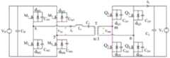
图1是双桥串联谐振变换器原理图;FIG1 is a schematic diagram of a dual-bridge series resonant converter;
图2是在双桥串联谐振变换器下采用无回流调制策略的稳态波形图;FIG2 is a steady-state waveform diagram of a dual-bridge series resonant converter using a non-return modulation strategy;
图3是双桥串联谐振变换器在时域下的等效电路图;FIG3 is an equivalent circuit diagram of a dual-bridge series resonant converter in the time domain;
图4是双桥串联谐振变换器全功率下的调制方案选择流程图;FIG4 is a flow chart of modulation scheme selection for a dual-bridge series resonant converter at full power;
图5是VH=150V,VL=80V,M=0.9,Pr=200W,vxy、vmn、ir、iL波形和各开关管电流图。FIG5 shows the waveforms ofvxy ,vmn , ir , and iL and the currents of the switch tubes whenVH = 150V,VL = 80V, M = 0.9, andPr = 200W.
具体实施方式DETAILED DESCRIPTION
本发明的原理是:通过调节脉宽α、β以及频率,在高功率采用固定波形脉宽调制,低功率采用固定波形频率调制,保持谐振电流与M1、Q1的门信号同相,不仅可以实现全开关管ZVS运行,还可以保证DBSRC一次侧与二次侧完全消除回流功率,提高整体运行效率。The principle of the present invention is: by adjusting the pulse width α, β and frequency, using fixed waveform pulse width modulation at high power and fixed waveform frequency modulation at low power, keeping the resonant current in phase with the gate signals ofM1 andQ1 , not only can the full switch tube ZVS operation be achieved, but also the return power on the primary and secondary sides of the DBSRC can be completely eliminated, thereby improving the overall operating efficiency.
实施例1:Embodiment 1:
如图1所示,一种双桥串联谐振变换器,包括依次相连的一次侧全桥、谐振槽、高频变压器和二次侧全桥。As shown in FIG1 , a dual-bridge series resonant converter includes a primary-side full bridge, a resonant tank, a high-frequency transformer and a secondary-side full bridge connected in sequence.
一次侧全桥包括开关管M1~M4,开关管M1~M4构成一次侧有源全桥电路;谐振槽包括设置在一次侧的依次连接的一次侧谐振电感Lr和谐振电容Cr;高频变压器的匝数比为n:1;二次侧全桥包括开关管Q1~Q4,开关管Q1~Q4构成二次侧有源全桥电路。The primary side full bridge includes switch tubesM1 -M4 ,which form aprimary side active full bridge circuit; the resonant tank includes a primary side resonant inductorLr and a resonant capacitorCr which are arranged on the primary side and connected insequence ; the turns ratio of the high frequency transformer is n:1; the secondary side full bridge includes switch tubesQ1 -Q4, which form a secondary side active full bridge circuit.
具体的,一次侧全桥电路由主电源VH、稳压电容CH、开关管M1~M4、体二极管dM1~dM4及其寄生电容CM1~CM4组成,经过由谐振电感Lr和谐振电容Cr组成的谐振槽和变比为n:1的高频变压器T,与由开关管Q1~Q4、体二极管dQ1~dQ4及其寄生电容CQ1~CQ4、滤波电容CL以及二次侧电压源VL组成的二次侧全桥电路相连。Specifically, the primary side full-bridge circuit is composed of a main power supplyVH , a voltage-stabilizing capacitorCH , switch tubesM1 ~M4 , body diodesdM1 ~dM4 and parasitic capacitorsCM1 ~CM4 , and is connected to a secondary side full-bridge circuit composed of switch tubesQ1 ~Q4 , body diodesdQ1 ~dQ4 and parasitic capacitorsCQ1 ~CQ4 , a filter capacitor CL and a secondary side voltage sourceVL through a resonant tank composed of a resonant inductorLr and a resonant capacitorCr and a high-frequency transformer T with a transformation ratio of n:1.
另一实施例,一种双桥串联谐振变换器的无回流调制方法,采用上述的一种双桥串联谐振变换器,调制方法包括以下步骤:Another embodiment, a non-return current modulation method of a double-bridge series resonant converter, using the above-mentioned double-bridge series resonant converter, the modulation method comprises the following steps:
S01:一个周期内,使得一次侧电压正负半周脉冲宽度可调,正负半周脉冲宽度为α,使得二次侧电压正负半周脉冲宽度可调,正负半周脉冲宽度为β;S01: In one cycle, the positive and negative half-cycle pulse widths of the primary side voltage are adjustable, and the positive and negative half-cycle pulse widths are α, and the positive and negative half-cycle pulse widths of the secondary side voltage are adjustable, and the positive and negative half-cycle pulse widths are β;
S02:调节二次侧电压滞后一次侧电压相位π-β,产生一个具有零电平的三电平交流电压波形,其正负脉宽为β;S02: Adjust the secondary side voltage to lag the primary side voltage phase by π-β, generating a three-level AC voltage waveform with zero level and positive and negative pulse widths of β;
S03:通过调节脉宽α、β以及频率,不同功率时采用固定波形脉宽调制或者固定波形频率调制,对谐振电流的相位进行调整,保持谐振电流与M1、Q1的门信号同相。S03: By adjusting the pulse width α, β and frequency, fixed waveform pulse width modulation or fixed waveform frequency modulation is used for different powers to adjust the phase of the resonant current and keep the resonant current in phase with the gate signal ofM1 andQ1 .
具体的实现中,如图2所示,调节开关管M1~M4的脉冲宽度,使开关管M1、M2、M3、M4保持50%占空比,且开关管M1和M2、M3和M4互补导通,调节开关管M3滞后M1角度α,产生一个具有零电平的三电平交流电压波形,其正负脉宽为α,0<α<π。In a specific implementation, as shown in FIG2 , the pulse widths of the switches M1 to M4 are adjusted so that the switch tubes M1 , M2 , M3 , and M4 maintain a 50% duty cycle, and the switch tubes M1 and M2 , M3 and M4 are complementarily turned on, and the switch tube M3 is adjusted to lag behind the switch tube M1 by an angle α, generating a three-level AC voltage waveform with a zero level, whose positive and negative pulse widths are α, 0<α<π.
调节开关管Q1~Q4的脉冲宽度,使开关管Q1、Q2、Q3、Q4保持50%占空比,且开关管Q1和Q2、Q3和Q4互补导通,调节开关管Q4滞后开关管Q1角度π-β,产生一个具有零电平的三电平交流电压波形,其正负脉宽为β,0<β<π。The pulse widths of the switches Q1 to Q4 are adjusted to keep the duty cycle of the switches Q1 , Q2 , Q3 , and Q4 at 50%, and the switches Q1 and Q2 , Q3 and Q4 are complementarily turned on, and the switch Q4 is adjusted to lag the switch Q1 by an angle π-β, generating a three-level AC voltage waveform with a zero level, whose positive and negative pulse widths are β, 0<β<π.
产生两个脉宽分别为α和β的三电平交流电压vxy和vmn。Generate two three-level AC voltagesvxy andvmn with pulse widths α and β respectively.
一实施例中,对谐振电流的相位进行调整;将谐振电流ir过零点调整在开关管M1与Q1的开启处,从而使得谐振电流与M1、Q1的门信号同相,即满足以下条件:ir,pu(ωst)=ir,pu(0)=0时,实现零回流功率。In one embodiment, the phase of the resonant current is adjusted; the zero-crossing point of the resonant current ir is adjusted at the turn-on point of the switch tubes M1 and Q1 , so that the resonant current is in phase with the gate signals of M1 and Q1 , that is, the following condition is satisfied: when ir,pu (ωs t)=ir,pu (0)=0, zero reflux power is achieved.
具体的实现,双桥串联谐振变换器在时域下的等效电路如图3所示:根据基波近似法,得到:For specific implementation, the equivalent circuit of the dual-bridge series resonant converter in the time domain is shown in Figure 3: According to the fundamental wave approximation method, we get:


其中,vxy(ωst)是vxy的时域表达形式,vmn(ωst)是vmn的时域表达形式;VH和VL分别是输入电压和输出电压;α和β分别是一次侧三电平交流电压的和二次侧三电平交流电压的脉冲宽度;Wherein,vxy (ωst ) is the time domain expression ofvxy ,vmn (ωst ) is the time domain expression ofvmn ;VH andVL are the input voltage and the output voltage respectively; α and β are the pulse widths of the primary side three-level AC voltage and the secondary side three-level AC voltage respectively;
进一步得到:Further we get:

其中,ir,pu是谐振电流ir的标幺化表达式,Ir,pu是标幺化谐振电流峰值,
具体表示为:Specifically expressed as:


其中,M是电压增益,表达式为


为了实现零回流功率,需要对谐振电流的相位进行调整。将谐振电流ir过零点调整在开关管M1与Q1的开启处,从而使得谐振电流与M1、Q1的门信号同相,因此无回流调制方法必须满足条件:ir,pu(ωst)=ir,pu(0)=0,具体表示为:In order to achieve zero reflux power, the phase of the resonant current needs to be adjusted. The zero-crossing point of the resonant current ir is adjusted to the opening point of the switch tubes M1 and Q1 , so that the resonant current is in phase with the gate signals of M1 and Q1. Therefore, the reflux-free modulation method must meet the condition: ir,pu (ωs t) = ir,pu (0) = 0, which can be specifically expressed as:

因此,保证零回流功率需要满足条件:Therefore, to ensure zero return power, the following conditions must be met:

根据电流和电压表达式可以得到标幺化输出功率PL,pu:The normalized output powerPL,pu can be obtained according to the current and voltage expressions:

由于谐振电流与M1、Q1的门信号同相,因此在开关管M1、M2、Q1与Q2的开通时刻,谐振电流为零;对于开关管M1、M2、Q1与Q2来说,在它们开通时,流过开关管的电流为零,也就是从零电流开通的ZVS运行,这种ZVS运行方式并没有增加变换器的开关损耗;对于其余的开关管,它们的ZVS运行方式为正常的负电流开通。Since the resonant current is in phase with the gate signals ofM1 andQ1 , the resonant current is zero when the switchesM1 , M2,Q1 andQ2 are turned on. For the switchesM1 ,M2 ,Q1 andQ2 , when theyare turned on, the current flowing through the switches is zero, that is, ZVS operation from zero current. This ZVS operation mode does not increase the switching loss of the converter. For the remaining switches, their ZVS operation mode is normal negative current turn-on.
由于谐振电流需要保持与M1、Q1的门信号同相,当电压增益M确定时,一次侧三电平交流电压的和二次侧三电平交流电压的脉冲宽度α和β调节范围受到限制,随着两个交流电压的占空比不断调节,越来越大,功率越来越小,当α或β调至最大值π时,此时仅用脉宽调制方案并不能满足变换器全功率范围运行;当变换器运行功率达到脉宽调制方案的临界功率时,需要采用频率调制来使得变换器能够在低功率下运行,具体方法为:保持两个交流电压占空比不变,通过调节变换器开关频率fs来达到使DBSRC在低功率下继续运行的目的,此过程实现方式的流程图如图4所示。Since the resonant current needs to be kept in phase with the gate signals ofM1 andQ1 , when the voltage gain M is determined, the adjustment range of the pulse widths α and β of the primary side three-level AC voltage and the secondary side three-level AC voltage is limited. As the duty cycle of the two AC voltages is continuously adjusted, they become larger and larger, and the power becomes smaller and smaller. When α or β is adjusted to the maximum value π, the pulse width modulation scheme alone cannot meet the full power range of the converter operation; when the converter operating power reaches the critical power of the pulse width modulation scheme, frequency modulation is required to enable the converter to operate at low power. The specific method is: keep the duty cycle of the two AC voltages unchanged, and adjust the converter switching frequencyfs to achieve the purpose of making the DBSRC continue to operate at low power. The flow chart of this process implementation method is shown in Figure 4.
其中,变换器的临界功率具体表示为:Among them, the critical power of the converter is specifically expressed as:

其中,PL,pu,boundary是脉宽调制与频率调制的分界标幺化输出功率,具体表达式由电压增益M确定。WherePL,pu,boundary is the boundary between pulse width modulation and frequency modulation, and the specific expression is determined by the voltage gain M.
如图4所示,当电压增益确定为M<1时,根据变换器的标幺化输出功率,确定变换器拟采用的调制方案:当变换器的标幺化输出功率大于PL,pu,boundary时,此时α<β≤π,DBSRC采用固定波形脉宽调制;当变换器的标幺化输出功率小于PL,pu,boundary时,此时β=π,DBSRC采用固定波形频率调制。当M确定为1时,此时α=β≤π,变换器无论是否大于PL,pu,boundary都采用固定波形脉宽调制。当M>1,变换器的标幺化输出功率大于PL,pu,boundary时,此时β<α≤π,DBRC采用固定波形脉宽调制;当变换器的标幺化输出功率小于PL,pu,boundary时,此时α=π,DBSRC采用固定波形频率调制。As shown in Figure 4, when the voltage gain is determined to be M<1, the modulation scheme to be adopted by the converter is determined according to the per-unit output power of the converter: when the per-unit output power of the converter is greater thanPL,pu,boundary , at this time α<β≤π, DBSRC adopts fixed waveform pulse width modulation; when the per-unit output power of the converter is less thanPL,pu,boundary , at this time β=π, DBSRC adopts fixed waveform frequency modulation. When M is determined to be 1, at this time α=β≤π, the converter adopts fixed waveform pulse width modulation regardless of whether it is greater thanPL,pu,boundary . When M>1, the per-unit output power of the converter is greater thanPL,pu,boundary , at this time β<α≤π, DBRC adopts fixed waveform pulse width modulation; when the per-unit output power of the converter is less thanPL,pu,boundary , at this time α=π, DBSRC adopts fixed waveform frequency modulation.
另一实施例中,一种双桥串联谐振变换器的无回流调制系统,采用上述的双桥串联谐振变换器,调制系统包括:In another embodiment, a non-return modulation system of a dual-bridge series resonant converter adopts the above-mentioned dual-bridge series resonant converter, and the modulation system includes:
一次侧波形调节模块,一个周期内,使得一次侧电压正负半周脉冲宽度可调,正负半周脉冲宽度为α;The primary side waveform adjustment module makes the positive and negative half-cycle pulse width of the primary side voltage adjustable within one cycle, and the positive and negative half-cycle pulse width is α;
二次侧波形调节模块,使得二次侧电压正负半周脉冲宽度可调,正负半周脉冲宽度为β;调节二次侧电压滞后一次侧电压相位π-β,产生一个具有零电平的三电平交流电压波形,其正负脉宽为β;The secondary side waveform adjustment module makes the positive and negative half-cycle pulse widths of the secondary side voltage adjustable, and the positive and negative half-cycle pulse widths are β; the secondary side voltage is adjusted to lag the primary side voltage phase by π-β, generating a three-level AC voltage waveform with a zero level, and its positive and negative pulse widths are β;
调制模块,通过调节脉宽α、β以及频率,不同功率时采用固定波形脉宽调制或者固定波形频率调制,对谐振电流的相位进行调整,保持谐振电流与M1、Q1的门信号同相。The modulation module adjusts the phase of the resonant current by adjusting the pulse width α, β and frequency, and adopts fixed waveform pulse width modulation or fixed waveform frequency modulation at different powers to keep the resonant current in phase with the gate signal ofM1 andQ1 .
具体的实现同上,这里不再赘述。The specific implementation is the same as above and will not be repeated here.
下一步进行关键参数设计:The next step is to design key parameters:
选择M=0.9,F=1.3,Q=1。设计输入电压VH为150V,输出电压VL为80V,额定功率Pr为200W,开关频率fs为100kHz。Select M = 0.9, F = 1.3, Q = 1. Design the input voltage VH to be 150V, the output voltage VL to be 80V, the rated power Pr to be 200W, and the switching frequency fs to be 100kHz.
因此关键参数可以得到:n=1.6875,RL=32Ω,Lr=188.5μH,Cr=22.71nF。Therefore, the key parameters can be obtained as follows: n = 1.6875,RL = 32Ω,Lr = 188.5μH,Cr = 22.71nF.
在M设计在0.9的情况下,DBSRC的脉宽调制与频率调制的分界标幺化输出功率值为:When M is designed to be 0.9, the demarcation between pulse width modulation and frequency modulation of DBSRC is the per-unit output power value:

此时,在选定的参数下200W的标幺功率值为0.81,150W的标幺功率值为0.61,100W的标幺功率值为0.405,50W的标幺功率值为0.203。也就是说,变换器在200W和150W下采用固定波形脉宽调制,在100W和50W下采用固定波形频率调制。At this time, under the selected parameters, the per-unit power value of 200W is 0.81, the per-unit power value of 150W is 0.61, the per-unit power value of 100W is 0.405, and the per-unit power value of 50W is 0.203. That is to say, the converter adopts fixed waveform pulse width modulation at 200W and 150W, and adopts fixed waveform frequency modulation at 100W and 50W.
为了验证理论分析,将采用以上参数在PSIM软件里进行仿真。In order to verify the theoretical analysis, the above parameters will be used to perform simulation in PSIM software.
接下来,将在4种负载情况(200W,150W,100W,50W)下进行仿真验证本发明的实际效果,如图5所示。在4种负载情况下,变换器全部开关管满足ZVS运行,一次侧与二次侧完全消除回流功率,并且二次侧输出电流几乎无环流,变换器效率大大提高。Next, simulations are performed under four load conditions (200W, 150W, 100W, and 50W) to verify the actual effect of the present invention, as shown in Figure 5. Under the four load conditions, all switches of the converter meet ZVS operation, the primary and secondary sides completely eliminate the reflux power, and the secondary side output current has almost no circulating current, and the converter efficiency is greatly improved.
上述实施例为本发明优选地实施方式,但本发明的实施方式并不受上述实施例的限制,其他的任何未背离本发明的精神实质与原理下所作的改变、修饰、替代、组合、简化,均应为等效的置换方式,都包含在本发明的保护范围之内。The above embodiments are preferred implementation modes of the present invention, but the implementation modes of the present invention are not limited to the above embodiments. Any other changes, modifications, substitutions, combinations, and simplifications that do not deviate from the spirit and principles of the present invention should be equivalent replacement methods and are included in the protection scope of the present invention.
Claims (10)


Priority Applications (1)
| Application Number | Priority Date | Filing Date | Title |
|---|---|---|---|
| CN202211687211.8ACN115955122B (en) | 2022-12-27 | 2022-12-27 | Reflux-free modulation method and system for double-bridge series resonant converter |
Applications Claiming Priority (1)
| Application Number | Priority Date | Filing Date | Title |
|---|---|---|---|
| CN202211687211.8ACN115955122B (en) | 2022-12-27 | 2022-12-27 | Reflux-free modulation method and system for double-bridge series resonant converter |
Publications (2)
| Publication Number | Publication Date |
|---|---|
| CN115955122Atrue CN115955122A (en) | 2023-04-11 |
| CN115955122B CN115955122B (en) | 2023-11-03 |
Family
ID=87287254
Family Applications (1)
| Application Number | Title | Priority Date | Filing Date |
|---|---|---|---|
| CN202211687211.8AActiveCN115955122B (en) | 2022-12-27 | 2022-12-27 | Reflux-free modulation method and system for double-bridge series resonant converter |
Country Status (1)
| Country | Link |
|---|---|
| CN (1) | CN115955122B (en) |
Cited By (2)
| Publication number | Priority date | Publication date | Assignee | Title |
|---|---|---|---|---|
| CN117937903A (en)* | 2024-02-05 | 2024-04-26 | 常熟理工学院 | Full-degree-of-freedom control method and system for DC-DC drive module of new energy vehicle |
| WO2024260029A1 (en)* | 2023-06-19 | 2024-12-26 | 常熟理工学院 | T-shaped lcl resonant converter and full-range soft-switching modulation method therefor |
Citations (5)
| Publication number | Priority date | Publication date | Assignee | Title |
|---|---|---|---|---|
| CN107968571A (en)* | 2017-11-27 | 2018-04-27 | 浙江大学 | A kind of double active three phase-shifting control methods of bridging parallel operation |
| CN110943606A (en)* | 2019-12-16 | 2020-03-31 | 北京理工大学 | Control method for power factor correction based on dual active bridge rectifier without current sampling |
| CN112117908A (en)* | 2020-08-11 | 2020-12-22 | 华中科技大学 | Frequency conversion phase shift modulation device and method for double-active-bridge series resonant converter circuit |
| CN114006536A (en)* | 2021-10-25 | 2022-02-01 | 联合汽车电子有限公司 | Double-active-bridge series resonant converter and control method thereof |
| CN114465489A (en)* | 2022-01-28 | 2022-05-10 | 常熟理工学院 | Full-half-bridge resonant converter and voltage balance control method thereof |
- 2022
- 2022-12-27CNCN202211687211.8Apatent/CN115955122B/enactiveActive
Patent Citations (5)
| Publication number | Priority date | Publication date | Assignee | Title |
|---|---|---|---|---|
| CN107968571A (en)* | 2017-11-27 | 2018-04-27 | 浙江大学 | A kind of double active three phase-shifting control methods of bridging parallel operation |
| CN110943606A (en)* | 2019-12-16 | 2020-03-31 | 北京理工大学 | Control method for power factor correction based on dual active bridge rectifier without current sampling |
| CN112117908A (en)* | 2020-08-11 | 2020-12-22 | 华中科技大学 | Frequency conversion phase shift modulation device and method for double-active-bridge series resonant converter circuit |
| CN114006536A (en)* | 2021-10-25 | 2022-02-01 | 联合汽车电子有限公司 | Double-active-bridge series resonant converter and control method thereof |
| CN114465489A (en)* | 2022-01-28 | 2022-05-10 | 常熟理工学院 | Full-half-bridge resonant converter and voltage balance control method thereof |
Non-Patent Citations (1)
| Title |
|---|
| 吴俊娟等: "串联谐振型双有源桥变换器的软开关特性研究", 太阳能学报, vol. 38, no. 11, pages 3005 - 3011* |
Cited By (2)
| Publication number | Priority date | Publication date | Assignee | Title |
|---|---|---|---|---|
| WO2024260029A1 (en)* | 2023-06-19 | 2024-12-26 | 常熟理工学院 | T-shaped lcl resonant converter and full-range soft-switching modulation method therefor |
| CN117937903A (en)* | 2024-02-05 | 2024-04-26 | 常熟理工学院 | Full-degree-of-freedom control method and system for DC-DC drive module of new energy vehicle |
Also Published As
| Publication number | Publication date |
|---|---|
| CN115955122B (en) | 2023-11-03 |
Similar Documents
| Publication | Publication Date | Title |
|---|---|---|
| WO2021077757A1 (en) | Wide gain control method for variable topology llc resonant converter | |
| CN111490683A (en) | Trajectory control method for double-transformer series resonance double-active bridge DC-DC converter topology | |
| Dusmez et al. | A fully integrated three-level isolated single-stage PFC converter | |
| CN108696140A (en) | Full-bridge resonance DC-DC converter with wide output voltage range and modulator approach | |
| CN112953245B (en) | Soft switching control method for full load range of dual active bridge converter | |
| CN106655785A (en) | Bidirectional hybrid bridge DC-DC converter and half-cycle volt-second area balance control method | |
| CN112928919A (en) | Isolated high-frequency resonant DC-DC converter with wide output voltage range and method | |
| CN108880268B (en) | Multi-mode control method of voltage source type semi-active bridge DC-DC converter | |
| CN108988646B (en) | DAB (digital audio broadcasting) optimization control method with voltage transmission ratio larger than 1 under zero-voltage switch | |
| CN115955122B (en) | Reflux-free modulation method and system for double-bridge series resonant converter | |
| CN106655781A (en) | LCC resonant converter PWM phase shift mixed control and efficiency optimization method | |
| CN114337344A (en) | Control method based on self-adaptive hybrid rectification multi-switch resonant LLC converter | |
| CN115833602B (en) | A double-transformer resonant converter and its modulation method | |
| CN114312382B (en) | System topology suitable for electric automobile wired wireless integrated charging pile | |
| CN110034686A (en) | Double active bridging parallel operations based on SiC-Si combined power semiconductor device switch | |
| EP4275271A1 (en) | An isolated bidirectional active-half-bridge resonant dc-dc power converter | |
| CN114142732A (en) | Comprehensive optimization modulation method for DAB converter | |
| Jin et al. | Hybrid control for three-level LLC resonant converter of dual-bridge for wide output range | |
| CN115864855A (en) | Control method for wide voltage range CLLLC resonant converter of energy storage system | |
| CN111835204A (en) | Zero-return power soft-switching modulation method and converter of resonant dual active bridge | |
| CN112636605B (en) | A DC conversion circuit and its mode switching control method in a wide voltage range | |
| CN109004836A (en) | Frequency conversion optimal control method suitable for modular multilevel commutator transformer | |
| CN117614236A (en) | A staggered parallel totem pole type power electronic transformer and its control method | |
| CN117458860A (en) | A wide-output LLC resonant converter topology and control method | |
| CN112953230A (en) | Triple phase-shifting control method and control device of double-active-bridge circuit |
Legal Events
| Date | Code | Title | Description |
|---|---|---|---|
| PB01 | Publication | ||
| PB01 | Publication | ||
| SE01 | Entry into force of request for substantive examination | ||
| SE01 | Entry into force of request for substantive examination | ||
| GR01 | Patent grant | ||
| GR01 | Patent grant |