CN115921259A - Ultrasonic transducer unit, preparation method thereof, and ultrasonic transducer device - Google Patents
Ultrasonic transducer unit, preparation method thereof, and ultrasonic transducer deviceDownload PDFInfo
- Publication number
- CN115921259A CN115921259ACN202310003044.9ACN202310003044ACN115921259ACN 115921259 ACN115921259 ACN 115921259ACN 202310003044 ACN202310003044 ACN 202310003044ACN 115921259 ACN115921259 ACN 115921259A
- Authority
- CN
- China
- Prior art keywords
- electrode
- substrate
- layer
- ultrasonic transducer
- orthographic projection
- Prior art date
- Legal status (The legal status is an assumption and is not a legal conclusion. Google has not performed a legal analysis and makes no representation as to the accuracy of the status listed.)
- Granted
Links
Images

Classifications
- Y—GENERAL TAGGING OF NEW TECHNOLOGICAL DEVELOPMENTS; GENERAL TAGGING OF CROSS-SECTIONAL TECHNOLOGIES SPANNING OVER SEVERAL SECTIONS OF THE IPC; TECHNICAL SUBJECTS COVERED BY FORMER USPC CROSS-REFERENCE ART COLLECTIONS [XRACs] AND DIGESTS
- Y02—TECHNOLOGIES OR APPLICATIONS FOR MITIGATION OR ADAPTATION AGAINST CLIMATE CHANGE
- Y02P—CLIMATE CHANGE MITIGATION TECHNOLOGIES IN THE PRODUCTION OR PROCESSING OF GOODS
- Y02P70/00—Climate change mitigation technologies in the production process for final industrial or consumer products
- Y02P70/50—Manufacturing or production processes characterised by the final manufactured product
Landscapes
- Transducers For Ultrasonic Waves (AREA)
Abstract
Description
Translated fromChinese技术领域technical field
本申请实施例涉及超声换能技术领域,具体而言,涉及一种超声换能单元及其制备方法、超声换能器件。The embodiments of the present application relate to the technical field of ultrasonic transducers, and in particular, to an ultrasonic transducer unit, a manufacturing method thereof, and an ultrasonic transducer device.
背景技术Background technique
超声波具有传播过程中方向集束性好和能量密度高的优点,同时又不会产生影响人生活和工作的噪音污染,更不像电磁波那样会产生电磁污染。因此,超声波工业、国防等很多领域都有广泛的应用。而在各种超声应用中,超声传感器都是其中最核心的器件。Ultrasonic waves have the advantages of good directionality and high energy density in the process of propagation, and at the same time, they will not produce noise pollution that affects people's life and work, and it will not produce electromagnetic pollution like electromagnetic waves. Therefore, ultrasonic industry, national defense and many other fields have a wide range of applications. In various ultrasonic applications, ultrasonic sensors are the core devices.
其中,电容式超声传感器(CMUT)因其无需添加额外的匹配层,相比传统的压电陶瓷(PZT)传感器有着更为广阔的应用前景。然而,电容式超声传感器需要在发射阶段单独施加直流偏压来克服薄膜张力,因此导致当前的电容式超声传感器功耗较大,成本较高。因此,如何有效降低电容式超声传感器的功耗和成本,成为当前亟待解决的技术问题。Among them, the capacitive ultrasonic sensor (CMUT) has a broader application prospect than the traditional piezoelectric ceramic (PZT) sensor because it does not need to add an additional matching layer. However, the capacitive ultrasonic sensor needs to apply a DC bias voltage separately in the transmitting stage to overcome the tension of the film, so the current capacitive ultrasonic sensor consumes a lot of power and has a high cost. Therefore, how to effectively reduce the power consumption and cost of the capacitive ultrasonic sensor has become an urgent technical problem to be solved.
发明内容Contents of the invention
本申请实施例在于提供一种超声换能单元及其制备方法、超声换能器件,旨在解决如何有效降低电容式超声传感器的功耗和成本的问题。The embodiment of the present application is to provide an ultrasonic transducer unit, a manufacturing method thereof, and an ultrasonic transducer device, aiming at solving the problem of how to effectively reduce the power consumption and cost of a capacitive ultrasonic sensor.
本申请实施例第一方面提供一种超声换能单元,包括:The first aspect of the embodiment of the present application provides an ultrasonic transducer unit, including:
衬底;Substrate;
第一电极,设置在所述衬底的一侧;a first electrode disposed on one side of the substrate;
第二电极,设置在所述第一电极背离所述衬底的一侧,且所述第一电极与所述第二电极之间存在空腔;a second electrode disposed on a side of the first electrode away from the substrate, and a cavity exists between the first electrode and the second electrode;
感光层,设置在所述第一电极靠近所述衬底一侧的表面,且所述感光层在所述衬底上的正投影与所述第一电极在所述衬底上的正投影至少部分交叠,或者设置在所述第二电极背离所述衬底一侧的表面,且所述感光层在所述衬底上的正投影与所述第二电极在所述衬底上的正投影至少部分交叠。The photosensitive layer is disposed on the surface of the first electrode close to the substrate, and the orthographic projection of the photosensitive layer on the substrate and the orthographic projection of the first electrode on the substrate are at least partially overlap, or be arranged on the surface of the second electrode away from the substrate, and the orthographic projection of the photosensitive layer on the substrate is the same as the orthographic projection of the second electrode on the substrate The projections overlap at least partially.
在一种可选的实施方式中,所述超声换能单元还包括支撑层,所述支撑层位于所述第二电极靠近所述衬底的一侧,所述第一电极以及所述支撑层围成所述空腔。In an optional embodiment, the ultrasonic transducer unit further includes a support layer, the support layer is located on the side of the second electrode close to the substrate, the first electrode and the support layer enclosing the cavity.
在一种可选的实施方式中,所述支撑层上具有刻蚀孔,所述刻蚀孔与所述空腔连通,所述刻蚀孔内填充所述感光层。In an optional implementation manner, the support layer has an etching hole, the etching hole communicates with the cavity, and the photosensitive layer is filled in the etching hole.
在一种可选的实施方式中,所述超声换能单元还包括第一钝化层,所述第一钝化层包括位于所述第二电极背离所述衬底一侧的第一部分和位于所述第二电极侧面的第二部分,且所述第一部分在所述衬底上的正投影与所述第二电极在所述衬底上的正投影边缘有交叠。In an optional implementation manner, the ultrasonic transducer unit further includes a first passivation layer, and the first passivation layer includes a first part located on the side of the second electrode away from the substrate and a first part located on the side of the second electrode away from the substrate. The second part of the side of the second electrode, and the orthographic projection of the first part on the substrate overlaps with the edge of the orthographic projection of the second electrode on the substrate.
在一种可选的实施方式中,所述第一钝化层具有由所述第一部分围成的开口区域,所述感光层填充所述开口区域。In an optional implementation manner, the first passivation layer has an opening area surrounded by the first portion, and the photosensitive layer fills the opening area.
在一种可选的实施方式中,所述第一部分在第一方向上的尺寸大于3μm,所述第一方向为与所述衬底的法线方向垂直的方向。In an optional implementation manner, a size of the first portion in a first direction is greater than 3 μm, and the first direction is a direction perpendicular to a normal direction of the substrate.
在一种可选的实施方式中,所述感光层设置在所述第二电极背离所述衬底一侧的表面,所述超声换能单元还包括第二钝化层,所述第二钝化层设置在所述感光层背离所述衬底的一侧,且所述第二钝化层在所述衬底上的正投影覆盖所述感光层在所述衬底上的正投影。In an optional implementation manner, the photosensitive layer is disposed on the surface of the second electrode away from the substrate, and the ultrasonic transducer unit further includes a second passivation layer, and the second passivation layer The passivation layer is disposed on the side of the photosensitive layer away from the substrate, and the orthographic projection of the second passivation layer on the substrate covers the orthographic projection of the photosensitive layer on the substrate.
在一种可选的实施方式中,所述感光层设置在所述第一电极靠近所述衬底一侧的表面,所述超声换能单元还包括第三钝化层,所述第三钝化层设置在所述第二电极背离所述衬底的一侧,且所述第三钝化层在所述衬底上的正投影覆盖所述第二电极在所述衬底上的正投影。In an optional implementation manner, the photosensitive layer is disposed on the surface of the first electrode close to the substrate, and the ultrasonic transducer unit further includes a third passivation layer, and the third passivation layer The passivation layer is disposed on the side of the second electrode away from the substrate, and the orthographic projection of the third passivation layer on the substrate covers the orthographic projection of the second electrode on the substrate .
本申请实施例第二方面提供一种超声换能器件,包括多个如第一方面所述的超声换能单元;The second aspect of the embodiment of the present application provides an ultrasonic transducer device, including a plurality of ultrasonic transducer units as described in the first aspect;
显示面板,用于向所述超声换能单元提供入射光线;a display panel, configured to provide incident light to the ultrasonic transducer unit;
驱动电路,用于向所述超声换能单元提供驱动信号;a driving circuit, configured to provide a driving signal to the ultrasonic transducer unit;
供电电路,用于向所述超声换能单元提供电源信号,所述电源信号包括直流电源信号和交流电源信号。The power supply circuit is used to provide a power signal to the ultrasonic transducer unit, and the power signal includes a DC power signal and an AC power signal.
本申请实施例第三方面提供一种超声换能单元的制备方法,包括:The third aspect of the embodiment of the present application provides a method for preparing an ultrasonic transducer unit, including:
提供衬底;provide the substrate;
提供第一电极,设置在所述衬底的一侧;providing a first electrode disposed on one side of the substrate;
提供第二电极,设置在所述第一电极背离所述衬底的一侧,且所述第一电极与所述第二电极之间存在空腔;providing a second electrode, disposed on a side of the first electrode away from the substrate, and a cavity exists between the first electrode and the second electrode;
提供感光层,设置在所述第一电极靠近所述衬底一侧的表面,且所述感光层在所述衬底上的正投影与所述第一电极在所述衬底上的正投影至少部分交叠,或者设置在所述第二电极背离所述衬底一侧的表面,且所述感光层在所述衬底上的正投影与所述第二电极在所述衬底上的正投影至少部分交叠。providing a photosensitive layer, disposed on the surface of the first electrode close to the substrate, and the orthographic projection of the photosensitive layer on the substrate and the orthographic projection of the first electrode on the substrate overlap at least partially, or be arranged on the surface of the second electrode facing away from the substrate, and the orthographic projection of the photosensitive layer on the substrate is the same as that of the second electrode on the substrate The orthographic projections overlap at least partially.
有益效果:Beneficial effect:
本申请实施例提供了一种超声换能单元及其制备方法、超声换能器件,包括:衬底;第一电极,设置在所述衬底的一侧;第二电极,设置在所述第一电极背离所述衬底的一侧,且所述第一电极与所述第二电极之间存在空腔;感光层,设置在所述第一电极靠近所述衬底一侧的表面,且所述感光层在所述衬底上的正投影与所述第一电极在所述衬底上的正投影至少部分交叠,或者设置在所述第二电极背离所述衬底一侧的表面,且所述感光层在所述衬底上的正投影与所述第二电极在所述衬底上的正投影至少部分交叠。本申请设置感光层使超声换能单元在接收到入射光线时产生静电力抵消振膜的张力,从而在发射阶段规避了直流电压的使用,有效降低了电容式超声传感器的功耗和成本。The embodiment of the present application provides an ultrasonic transducer unit and its preparation method, and an ultrasonic transducer device, including: a substrate; a first electrode arranged on one side of the substrate; a second electrode arranged on the first electrode An electrode is away from the side of the substrate, and there is a cavity between the first electrode and the second electrode; a photosensitive layer is arranged on the surface of the first electrode close to the substrate, and The orthographic projection of the photosensitive layer on the substrate at least partially overlaps the orthographic projection of the first electrode on the substrate, or is arranged on the surface of the second electrode on a side away from the substrate , and the orthographic projection of the photosensitive layer on the substrate at least partially overlaps the orthographic projection of the second electrode on the substrate. The application sets the photosensitive layer so that the ultrasonic transducer unit generates electrostatic force to offset the tension of the diaphragm when receiving incident light, thereby avoiding the use of DC voltage in the transmission stage and effectively reducing the power consumption and cost of the capacitive ultrasonic sensor.
附图说明Description of drawings
为了更清楚地说明本申请实施例的技术方案,下面将对本申请实施例的描述中所需要使用的附图作简单地介绍,显而易见地,下面描述中的附图仅仅是本申请的一些实施例,对于本领域普通技术人员来讲,在不付出创造性劳动性的前提下,还可以根据这些附图获得其他的附图。In order to more clearly illustrate the technical solutions of the embodiments of the present application, the following will briefly introduce the accompanying drawings that need to be used in the description of the embodiments of the present application. Obviously, the accompanying drawings in the following description are only some embodiments of the present application , for those skilled in the art, other drawings can also be obtained according to these drawings without paying creative labor.
图1是本申请一实施例提出的一种超声换能单元结构示意图;Fig. 1 is a schematic structural diagram of an ultrasonic transducer unit proposed by an embodiment of the present application;
图2是本申请一实施例提出的一种感光层在第二电极表面的超声换能单元结构示意图;Fig. 2 is a schematic structural diagram of an ultrasonic transducer unit with a photosensitive layer on the surface of a second electrode proposed by an embodiment of the present application;
图3是本申请一实施例提出的一种包含第四钝化层的超声换能单元结构示意图;Fig. 3 is a schematic structural diagram of an ultrasonic transducer unit including a fourth passivation layer proposed by an embodiment of the present application;
图4是本申请一实施例提出的一种包含第二钝化层的超声换能单元结构示意图。Fig. 4 is a schematic structural diagram of an ultrasonic transducer unit including a second passivation layer proposed by an embodiment of the present application.
附图标记说明:101、衬底;102、第一电极;103、第二电极;1031、第一电极层;1032、第二电极层;104、感光层;105、支撑层;106、第一钝化层;1061、第一部分;1062、第二部分;107、第四钝化层;108、第二钝化层;109、第三钝化层。Description of reference numerals: 101, substrate; 102, first electrode; 103, second electrode; 1031, first electrode layer; 1032, second electrode layer; 104, photosensitive layer; 105, support layer; 106, first Passivation layer; 1061, first part; 1062, second part; 107, fourth passivation layer; 108, second passivation layer; 109, third passivation layer.
具体实施方式Detailed ways
下面将结合本申请实施例中的附图,对本申请实施例中的技术方案进行清楚、完整地描述,显然,所描述的实施例是本申请一部分实施例,而不是全部的实施例。基于本申请中的实施例,本领域普通技术人员在没有做出创造性劳动前提下所获得的所有其他实施例,都属于本申请保护的范围。The following will clearly and completely describe the technical solutions in the embodiments of the present application with reference to the drawings in the embodiments of the present application. Obviously, the described embodiments are part of the embodiments of the present application, not all of them. Based on the embodiments in this application, all other embodiments obtained by persons of ordinary skill in the art without making creative efforts belong to the scope of protection of this application.
超声波具有传播过程中方向集束性好和能量密度高的优点,同时又不会产生影响人生活和工作的噪音污染,更不像电磁波那样会产生电磁污染。因此,超声波工业、国防等很多领域都有广泛的应用。如在国防领域中,超声被各国军队广泛用于水下探测潜艇位置,这种军事应用需要把超声技术从传感器制造推进到超声成像中去。同时超声波也可用于超声诊断,超声探伤,超声检测以及超声波抛光,超声波搅拌,超声波治疗,超声成像,超声解调可听声等。Ultrasonic waves have the advantages of good directionality and high energy density in the process of propagation, and at the same time, they will not produce noise pollution that affects people's life and work, and it will not produce electromagnetic pollution like electromagnetic waves. Therefore, ultrasonic industry, national defense and many other fields have a wide range of applications. For example, in the field of national defense, ultrasound is widely used by the armies of various countries to detect the position of submarines underwater. This military application needs to advance ultrasonic technology from sensor manufacturing to ultrasonic imaging. At the same time, ultrasound can also be used for ultrasonic diagnosis, ultrasonic flaw detection, ultrasonic testing, ultrasonic polishing, ultrasonic stirring, ultrasonic therapy, ultrasonic imaging, ultrasonic demodulation of audible sound, etc.
而在各种超声应用中,超声传感器都是其中最核心的器件。然而到目前为止,压电陶瓷(PZT)传感器几乎占据了上述领域的全部市场。但同时它也存在着天然的缺陷:PZT晶片与工作介质如空气,水之间的阻抗失配,不仅会降低界面的声波透射系数,还会严重的影响传感器的灵敏度,于是需要我们在压电材料和工作介质之间添加一层匹配层来克服这个问题,但这样又会产生两个新问题,一是匹配层会使器件的带宽变窄;二是由于要求的匹配层较薄,很难找到合适的匹配层。因此寻找新的传感器来取代PZT传感器就尤显迫切。In various ultrasonic applications, ultrasonic sensors are the core devices. However, until now, piezoelectric ceramic (PZT) sensors have occupied almost the entire market in the above-mentioned fields. But at the same time, it also has natural defects: the impedance mismatch between the PZT chip and the working medium such as air and water will not only reduce the acoustic transmission coefficient of the interface, but also seriously affect the sensitivity of the sensor. A matching layer is added between the material and the working medium to overcome this problem, but this will cause two new problems. One is that the matching layer will narrow the bandwidth of the device; the other is that the required matching layer is thin and it is difficult to Find the right matching layer. Therefore, it is particularly urgent to find new sensors to replace PZT sensors.
相关技术中,电容式超声传感器(CMUT)因其无需添加额外的匹配层,相比传统的压电陶瓷(PZT)传感器有着更为广阔的应用前景。然而,电容式超声传感器中超声波的产生需要振膜发生共振推动周围介质做功产生超声波,而振膜的振动需要克服振膜本身的薄膜张力,如果直接在振膜施加交流电压来使振膜发生振动,则因需要克服薄膜张力提供较大的交流电压,导致超声传感器的功耗大幅提升。为了克服振膜本身的薄膜张力,需要在发射阶段先单独施加直流偏压来克服振膜的张力,来降低后续使振膜发生振动时所需的交流电压,但是直流电压在发射阶段的使用仍会导致当前的电容式超声传感器功耗较大,成本较高。In the related art, the capacitive ultrasonic sensor (CMUT) has a wider application prospect than the traditional piezoelectric ceramic (PZT) sensor because it does not need to add an additional matching layer. However, the generation of ultrasonic waves in capacitive ultrasonic sensors requires the diaphragm to resonate to push the surrounding medium to do work to generate ultrasonic waves, and the vibration of the diaphragm needs to overcome the film tension of the diaphragm itself. If an AC voltage is directly applied to the diaphragm to vibrate the diaphragm , the power consumption of the ultrasonic sensor is greatly increased due to the need to overcome the tension of the film and provide a larger AC voltage. In order to overcome the film tension of the diaphragm itself, it is necessary to apply a DC bias voltage alone to overcome the tension of the diaphragm in the launch phase, so as to reduce the subsequent AC voltage required to vibrate the diaphragm, but the use of DC voltage in the launch phase is still It will cause the current capacitive ultrasonic sensor to consume more power and cost more.
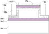
有鉴于此,本申请实施例提出一种超声换能单元,图1示出了一种超声换能单元结构示意图,如图1所示,包括:衬底101,第一电极102,第二电极103以及感光层104。其中,第一电极102设置在所述衬底101的一侧;第二电极103设置在所述第一电极102背离所述衬底101的一侧,且所述第一电极102与所述第二电极103之间存在空腔。In view of this, an embodiment of the present application proposes an ultrasonic transducer unit. FIG. 1 shows a schematic structural diagram of an ultrasonic transducer unit. As shown in FIG. 1 , it includes: a
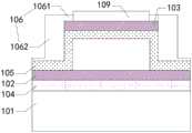
所述感光层104设置在所述第一电极102靠近所述衬底101一侧的表面,图2示出了一种感光层在第二电极表面的超声换能单元结构示意图,如图2所示,所述感光层104在所述衬底101上的正投影与所述第一电极102在所述衬底101上的正投影至少部分交叠;或者所述感光层104设置在所述第二电极103背离所述衬底101一侧的表面,如图1所示,所述感光层104在所述衬底101上的正投影与所述第二电极103在所述衬底101上的正投影至少部分交叠。The
具体而言,所述超声换能单元中的感光层104设置在靠近入射光线的入光方向的电极靠近入光方向的一侧。在所述入光方向为第二电极103指向第一电极102的方向时,所述感光层104设置在所述第二电极103背离所述衬底101一侧的表面;在所述入光方向为第一电极102指向第二电极103的方向时,所述感光层104设置在所述第一电极102靠近所述衬底101一侧的表面。Specifically, the
在所述感光层104设置在所述第二电极103背离所述衬底101一侧的表面的情况下,当所述感光层104接收到由第二电极103指向第一电极102的方向的入射光线的照射时,所述感光层104受到入射光线的激发生成光生电荷,所述光生电荷集中在所述感光层所接触的第二电极103背离所述衬底的一面上;同时在第一电极102上感应产生与光生电荷电性相反的电荷。第一电极102和第二电极103之间的电荷使第二电极103产生直流偏置电压,生成作用于振膜(包括位于所述空腔背离所述衬底一侧的多层膜结构),受力方向指向衬底101的静电力,随着作用于振膜的静电力继续增大,振膜向衬底101方向的位移不断增加;振膜本身具有指向背离衬底方向的薄膜张力,当静电力与薄膜张力达到平衡时,完成对振膜本身的薄膜张力的抵消。此时施加于第二电极103的交流电压无需再克服薄膜张力,因此只要在第二电极103上施加一个小信号的交流电压,即可使振膜产生振动生成超声波。In the case where the
在所述感光层104设置在所述第一电极102靠近所述衬底101一侧的表面的情况下,当所述感光层104接收到由第一电极102指向第二电极103的方向的入射光线的照射时,所述感光层104受到入射光线的激发生成光生电荷,所述光生电荷集中在所述感光层所接触的第一电极102靠近所述衬底的一面上;同时在第二电极103上感应产生与光生电荷电性相反的电荷。第一电极102和第二电极103之间的电荷使第二电极103产生直流偏置电压,生成作用于振膜(包括位于所述空腔背离所述衬底一侧的多层膜结构),受力方向指向衬底101的静电力,随着作用于振膜的静电力继续增大,振膜向衬底101方向的位移不断增加;振膜本身具有指向背离衬底方向的薄膜张力,当静电力与薄膜张力达到平衡时,完成对振膜本身的薄膜张力的抵消。此时施加于第二电极103的交流电压无需再克服薄膜张力,因此只要在第二电极103上施加一个小信号的交流电压,即可使振膜产生振动。In the case where the
本申请通过设置感光层104,在接收到入射光线后自动生成光生电荷,在第二电极103处产生静电力来有效抵消薄膜张力,无需额外向第二电极103施加直流偏压来抵消薄膜张力,从而在超声波的发射阶段规避了直流电压的使用,有效降低了电容式超声传感器的功耗和成本。In this application, by setting the
其中,所述感光层可以选用现有技术中的感光材料,如PIN光电二极管、OPD(Organic Photodetector)等,所述第一电极102的材料为导电金属材料,如Cu、Mo、Al等,所述第二电极103的材料为导电金属材料(如Cu、Mo、Al等)或半导体材料(如ITO等),具体感光层、第一电极和第二电极的材料本申请实施例不作具体限制。Wherein, the photosensitive layer can be selected from photosensitive materials in the prior art, such as PIN photodiode, OPD (Organic Photodetector), etc., and the material of the
在一种可选的实施方式中,所述超声换能单元还包括支撑层105,所述支撑层105位于所述第二电极103靠近所述衬底101的一侧,所述第一电极102以及所述支撑层105围成所述空腔。在超声换能单元发射或接收超声波时,第二电极103会发生振动,为了防止在第二电极103振动时与第一电极102接触造成漏电或短路等不良现象,在第一电极102与第二电极103之间形成所述空腔,该空腔用作发生振动的第二电极103可振动空间,并通过支撑层105将第二电极103与空腔分隔开。In an optional implementation manner, the ultrasonic transducer unit further includes a
需要说明的是,所述空腔的形状可以为圆形、方型、多边形或其他不规则图形中的一种,具体空腔的形状可根据实际情况确定,本申请在此不作限制。此外,空腔的尺寸可根据振膜厚度和谐振频率计算得到,具体按照如下公式进行计算:It should be noted that the shape of the cavity can be one of circular, square, polygonal or other irregular figures, and the specific shape of the cavity can be determined according to actual conditions, and the present application does not make a limitation here. In addition, the size of the cavity can be calculated according to the thickness of the diaphragm and the resonance frequency, specifically according to the following formula:

其中,f为所述谐振频率;t为所述振膜厚度;a为所述空腔的尺寸;Y0为杨氏模量;ρ为振膜密度;σ为泊松比。Wherein, f is the resonant frequency; t is the thickness of the diaphragm; a is the size of the cavity; Y0 is the Young's modulus; ρ is the density of the diaphragm; σ is the Poisson's ratio.
其中,支撑层105的材料可以为:氮化硅(SiNx)、氧化硅(SiOx)或多晶硅(poly-Si)中的一种。具体支撑层的材料可以根据实际情况进行确定,本申请在此不作限制。Wherein, the material of the
在一种可选的实施方式中,所述支撑层105上具有刻蚀孔,所述支撑层105上的刻蚀孔位于所述支撑层105的侧面,所述刻蚀孔与所述空腔连通,用于在制备过程中刻蚀出所述空腔。此外,所述刻蚀孔内填充所述感光层材料,用于将工作介质与空腔内的空间分隔开,防止工作介质(如水、空气等)通过刻蚀孔进入第一电极102与第二电极103之间的空腔内部,防止对第二电极102的振动产生不良影响。In an optional embodiment, the
在一种可选的实施方式中,所述超声换能单元还包括第一钝化层106,所述第一钝化层106包括位于所述第二电极103背离所述衬底101一侧的第一部分1061和位于所述第二电极103侧面的第二部分1062,且所述第一部分1061在所述衬底101上的正投影与所述第二电极103在所述衬底101上的正投影边缘有交叠。In an optional implementation manner, the ultrasonic transducer unit further includes a
其中,为了防止刻蚀空腔的过程中对第二电极103产生误刻蚀而对第二电极103造成不良影响,在第二电极103的侧面设置第一钝化层106,第一钝化层106包括位于第二电极背离所述衬底101一侧的第一部分1061以及位于第二电极103侧面的第二部分1062,保护第二电极103的侧面不会被误刻蚀。在一种可选的实施方式中,所述第一部分1061在第一方向上的尺寸大于3μm,所述第一方向为与所述衬底的法线方向垂直的方向。Wherein, in order to prevent the
其中,第一钝化层106的材料可以为:氮化硅(SiNx)、氧化硅(SiOx)或多晶硅(poly-Si)中的一种。具体的第一钝化层的材料可以根据实际情况进行确定,本申请在此不作限制。Wherein, the material of the
其中,第一钝化层106的第一部分1061在第二电极103背离所述衬底101一侧的表面上围成开口区域,该开口区域填充所述感光层104,形成如图1所示的设置在所述第二电极103背离所述衬底101一侧的表面的感光层104。Wherein, the
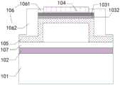
在一种可选的实施方式中,所述第一电极102背离所述衬底101的一侧还设置有第四钝化层107,图3示出了一种包含第四钝化层的超声换能单元结构示意图,如图3所示,所述第四钝化层设置在所述第一电极102和所述支撑层105之间,第四钝化层107与所述支撑层105围成所述空腔。通过设置所述第四钝化层107,对第一电极102进行保护,避免在刻蚀空腔时从支撑层105的刻蚀孔进入的刻蚀液与第一电极102背离衬底101一侧的表面接触而对第一电极102产生误刻蚀。In an optional implementation manner, the side of the
其中,第四钝化层107的材料可以为:氮化硅(SiNx)、氧化硅(SiOx)或多晶硅(poly-Si)中的一种。具体的第四钝化层的材料可以根据实际情况进行确定,本申请在此不作限制。Wherein, the material of the fourth passivation layer 107 may be one of silicon nitride (SiNx ), silicon oxide (SiOx ) or polysilicon (poly-Si). The specific material of the fourth passivation layer can be determined according to the actual situation, which is not limited in this application.
在一种可选的实施方式中,如图3所示,所述第二电极103为包括第一电极层1031和第二电极层1032的复合结构。其中,所述第二电极层1032设置在所述支撑层105背离所述衬底101的一侧,所述第一电极层1031位于所述第二电极层1032背离所述衬底101一侧的表面,且所述第一电极层1031在所述衬底101上的正投影覆盖所述第二电极层1032在所述衬底101上的正投影,或者所述第一电极层1031在所述衬底101上的正投影与所述第二电极层1032在所述衬底101上的正投影重合。其中,第一电极层1031的材料与第二电极层1032的材料的针对于刻蚀空腔的刻蚀液的刻蚀选择比越低越好,所述第一电极层1031用于防止刻蚀液在刻蚀空腔时接触第二电极的第二电极层1032,保护所述第二电极层1032不会受到刻蚀空腔的刻蚀液的误刻蚀。示例性地,所述第一电极层1031的材料为ITO(氧化铟锡),所述第二电极层1032的材料为Mo(钼),此时刻蚀空腔的刻蚀液对第一电极层1031的刻蚀效果较差,对第二电极层1032的刻蚀效果较好,第一电极层可以有效包括第二电极层不被误刻蚀。需要说明的是,第一电极层可以为半导体材料,第二电极层可以为金属材料,上述示例只是为了更好的使本领域技术人员理解本申请而提供的一种可选地具体实例,具体的第一电极层1031和第二电极层1032的材料不局限于这一种情况。In an optional implementation manner, as shown in FIG. 3 , the
在一种可选的实施方式中,所述第一电极102靠近所述衬底101的一侧还设置有缓冲层。In an optional implementation manner, a buffer layer is further provided on a side of the
在一种可选的实施方式中,所述感光层104设置在所述第二电极103背离所述衬底101一侧的表面,所述超声换能单元还包括第二钝化层108,图4示出了一种包含第二钝化层的超声换能单元结构示意图,如图4所示,所述第二钝化层108设置在所述感光层104背离所述衬底101的一侧,且所述第二钝化层108在所述衬底101上的正投影覆盖所述感光层104在所述衬底101上的正投影。第二钝化层108用于将工作介质与感光层104以及第二电极103分隔开,防止工作介质对感光层104以及第二电极103造成不良影响。此时,感光层104只用于光电换能,因此感光层可以选用现有技术中的感光材料,如有机光电器件PIN光电二极管、OPD(Organic Photodetector)等;第二钝化层108的材料可以为:氮化硅(SiNx)、氧化硅(SiOx)或多晶硅(poly-Si)中的一种。具体的第二钝化层的材料可以根据实际情况进行确定,本申请在此不作限制。In an optional implementation manner, the
在一种可选的实施方式中,所述感光层104复用为所述第二钝化层,如图1所示,此时所述感光层104直接与工作介质接触,用于将工作介质与第二电极103背离衬底101一侧的表面分隔开,防止工作介质对第二电极103造成不良影响。通过将所述感光层104复用为第二钝化层,使本申请提供的超声换能单元的膜层数不会因设置感光层而额外增加,从而降低了超声换能单元的生产成本。需要说明的是,当所述感光层104复用为第二钝化层时,所述感光层104的材料为能够在工作介质中具有稳定性的感光材料,如PIN结构材料,具体复用为第二钝化层的感光层的材料可选择现有技术中在工作介质中具有稳定性的感光材料,本申请在此不作限制。In an optional implementation manner, the
在一种可选的实施方式中,如图2所示,所述感光层104设置在所述第一电极102靠近所述衬底101一侧的表面,所述感光层104在所述衬底101上的正投影与所述第二电极103在所述衬底101上的正投影至少部分交叠。其中,所述超声换能单元还包括第三钝化层109,所述第三钝化层109设置在所述第二电极103背离所述衬底101的一侧,且所述第三钝化层109在所述衬底101上的正投影覆盖所述第二电极103在所述衬底上的正投影。In an optional implementation manner, as shown in FIG. 2, the
其中,第三钝化层109用于将工作介质与第二电极103分隔开,防止工作介质对第二电极103造成不良影响。第三钝化层109的材料可以为:氮化硅(SiNx)、氧化硅(SiOx)或多晶硅(poly-Si)中的一种。具体的第三钝化层的材料可以根据实际情况进行确定,本申请在此不作限制。Wherein, the
本申请实施例中,所述第二电极103、支撑层105与所述第二电极接触的部分、以及第二电极103背离所述衬底一侧设置的层一起作为振膜。具体而言,在所述感光层104设置在所述第二电极103背离所述衬底101一侧的表面的情况下,所述第二电极103、支撑层105与所述第二电极接触的部分、以及感光层104一起作为振膜;在所述感光层104设置在所述第一电极102背离所述衬底101一侧的表面的情况下,所述第二电极103、支撑层105与所述第二电极接触的部分、以及第三钝化层109一起作为振膜。In the embodiment of the present application, the
在超声波发射阶段,第二电极103接收小信号的交流电压而进行振动,振膜的振动推动周围的工作介质做功产生超声波,实现超声波的发射;在超声波接收阶段,第一电极102和第二电极103之间施加有固定的直流偏置电压,工作介质传播的超声波会使振膜引起谐波振动,从而使超声换能单元的电容发生改变,超声换能单元的电容变化导致电流在外部电路中流动,该电流被放大以进行下一步电路处理。即可以检测周围工作介质的超声波信息。In the ultrasonic emission stage, the
本申请实施例提供了一种超声换能单元,包括:衬底;第一电极,设置在所述衬底的一侧;第二电极,设置在所述第一电极背离所述衬底的一侧,且所述第一电极与所述第二电极之间存在空腔;感光层,设置在所述第一电极靠近所述衬底一侧的表面,且所述感光层在所述衬底上的正投影与所述第一电极在所述衬底上的正投影至少部分交叠,或者设置在所述第二电极背离所述衬底一侧的表面,且所述感光层在所述衬底上的正投影与所述第二电极在所述衬底上的正投影至少部分交叠。本申请设置感光层使超声换能单元在接收到入射光线时产生静电力抵消振膜的张力,从而在发射阶段规避了直流电压的使用,有效降低了电容式超声传感器的功耗和成本。An embodiment of the present application provides an ultrasonic transducer unit, comprising: a substrate; a first electrode disposed on one side of the substrate; a second electrode disposed on a side of the first electrode away from the substrate side, and there is a cavity between the first electrode and the second electrode; the photosensitive layer is arranged on the surface of the first electrode close to the substrate, and the photosensitive layer is on the substrate The orthographic projection on the substrate at least partially overlaps with the orthographic projection of the first electrode on the substrate, or is arranged on the surface of the second electrode on the side away from the substrate, and the photosensitive layer is on the substrate The orthographic projection on the substrate at least partially overlaps the orthographic projection of the second electrode on the substrate. The application sets the photosensitive layer so that the ultrasonic transducer unit generates electrostatic force to offset the tension of the diaphragm when receiving incident light, thereby avoiding the use of DC voltage in the transmission stage and effectively reducing the power consumption and cost of the capacitive ultrasonic sensor.
基于同一发明构思,本申请实施例提供一种超声换能器件,包括多个如上所述的超声换能单元、驱动电路和供电电路。其中,驱动电路用于向所述显示面板提供驱动信号,供电电路用于向所述显示面板提供电源信号。Based on the same inventive concept, an embodiment of the present application provides an ultrasonic transducer device, including a plurality of ultrasonic transducer units as described above, a driving circuit, and a power supply circuit. Wherein, the driving circuit is used to provide a driving signal to the display panel, and the power supply circuit is used to provide a power signal to the display panel.
本申请实施例中,所述电源信号包括直流电源信号和交流电源信号。其中,在超声发射阶段,所述供电电路与所述超声换能单元的第二电极相连接,向所述超声换能单元的第二电极提供交流电源信号;在超声接收阶段,所述供电电路与所述超声换能单元的第一电极以及第二电极相连接,向所述超声换能单元的第一电极与第二电极之间提供直流电源信号。In the embodiment of the present application, the power signal includes a DC power signal and an AC power signal. Wherein, in the ultrasonic transmitting stage, the power supply circuit is connected to the second electrode of the ultrasonic transducer unit, and provides an AC power signal to the second electrode of the ultrasonic transducer unit; in the ultrasonic receiving stage, the power supply circuit It is connected with the first electrode and the second electrode of the ultrasonic transducing unit, and provides a DC power signal between the first electrode and the second electrode of the ultrasonic transducing unit.
基于同一发明构思,本申请实施例提供一种超声换能单元的制备方法,包括:Based on the same inventive concept, an embodiment of the present application provides a method for preparing an ultrasonic transducer unit, including:
提供衬底。Provide the substrate.
提供第一电极,设置在所述衬底的一侧。A first electrode is provided disposed on one side of the substrate.
提供第二电极,设置在所述第一电极背离所述衬底的一侧,且所述第一电极与所述第二电极之间存在空腔。A second electrode is provided, disposed on a side of the first electrode away from the substrate, and a cavity exists between the first electrode and the second electrode.
提供感光层,设置在所述第一电极靠近所述衬底一侧的表面,且所述感光层在所述衬底上的正投影与所述第一电极在所述衬底上的正投影至少部分交叠,或者设置在所述第二电极背离所述衬底一侧的表面,且所述感光层在所述衬底上的正投影与所述第二电极在所述衬底上的正投影至少部分交叠。providing a photosensitive layer, disposed on the surface of the first electrode close to the substrate, and the orthographic projection of the photosensitive layer on the substrate and the orthographic projection of the first electrode on the substrate overlap at least partially, or be arranged on the surface of the second electrode facing away from the substrate, and the orthographic projection of the photosensitive layer on the substrate is the same as that of the second electrode on the substrate The orthographic projections overlap at least partially.
具体制备第一电极时,在所述衬底的一侧形成第一电极材料层,对第一电极材料层背离所述衬底的一侧表面进行曝光、刻蚀,形成第一电极的电极图案,随后去除残留光刻胶,形成所述第一电极。其中,第一电极材料层可以为导电金属材料,如Cu、Mo、Al等。When specifically preparing the first electrode, a first electrode material layer is formed on one side of the substrate, and the surface of the first electrode material layer away from the substrate is exposed and etched to form an electrode pattern of the first electrode , and then remove the residual photoresist to form the first electrode. Wherein, the first electrode material layer may be a conductive metal material, such as Cu, Mo, Al and the like.
在一种可选的实施方式中,先在所述衬底的一侧形成缓冲层;在所述缓冲层背离所述衬底的一侧形成第一电极材料层,对第一电极材料层背离所述衬底的一侧表面进行曝光、刻蚀,形成第一电极的电极图案,随后去除残留光刻胶,形成所述第一电极。In an optional implementation manner, a buffer layer is first formed on one side of the substrate; a first electrode material layer is formed on the side of the buffer layer away from the substrate, and the first electrode material layer is away from the substrate. One side surface of the substrate is exposed and etched to form an electrode pattern of the first electrode, and then the residual photoresist is removed to form the first electrode.
在一种可选的实施方式中,在形成所述第一电极之后,在所述第一电极背离所述衬底的一侧形成第四钝化层,所述第四钝化层的材料可以为:氮化硅(SiNx)、氧化硅(SiOx)或多晶硅(poly-Si)中的一种。具体的第四钝化层的材料可以根据实际情况进行确定,本申请在此不作限制。In an optional implementation manner, after forming the first electrode, a fourth passivation layer is formed on the side of the first electrode away from the substrate, and the material of the fourth passivation layer can be It is one of silicon nitride (SiNx ), silicon oxide (SiOx ) or polysilicon (poly-Si). The specific material of the fourth passivation layer can be determined according to the actual situation, which is not limited in this application.
具体制备第二电极时,在所述第一电极背离所述衬底的一侧的第一目标区域内形成牺牲层,所述牺牲层的材料为刻蚀速率较快、表面平整度较好的金属材料,如Mo等。在形成所述牺牲层之后,在所述牺牲层背离所述衬底的一侧表面以及侧面形成支撑层,并在所述支撑层侧面的第二目标区域内刻蚀出刻蚀孔,使所述刻蚀孔中暴露所述牺牲层。其中,所述支撑层的材料可以为:氮化硅(SiNx)、氧化硅(SiOx)或多晶硅(poly-Si)中的一种。When specifically preparing the second electrode, a sacrificial layer is formed in the first target region on the side of the first electrode away from the substrate, and the material of the sacrificial layer is one with a faster etching rate and better surface smoothness. Metal materials, such as Mo, etc. After forming the sacrificial layer, a supporting layer is formed on the surface and side of the sacrificial layer away from the substrate, and etching holes are etched in the second target area on the side of the supporting layer, so that the The sacrificial layer is exposed in the etching hole. Wherein, the material of the supporting layer may be one of silicon nitride (SiNx ), silicon oxide (SiOx ) or polycrystalline silicon (poly-Si).
在所述支撑层背离所述衬底的一侧形成第二电极,所述第二电极材料层,对第二电极材料层背离所述衬底的一侧表面进行曝光、刻蚀,形成第二电极的电极图案,随后去除残留光刻胶,形成所述第二电极。其中,第二电极材料层可以为导电金属材料,如Cu、Mo、Al等,也可以为半导体材料,如ITO等。随后,通过所述支撑层的刻蚀孔注入刻蚀液将牺牲层刻蚀去除,形成空腔。A second electrode is formed on the side of the support layer away from the substrate, and the second electrode material layer exposes and etches the surface of the second electrode material layer away from the substrate to form a second electrode material layer. The electrode pattern of the electrode, and then remove the residual photoresist to form the second electrode. Wherein, the second electrode material layer may be a conductive metal material, such as Cu, Mo, Al, etc., or a semiconductor material, such as ITO. Subsequently, an etchant is injected through the etching holes of the supporting layer to etch and remove the sacrificial layer to form a cavity.
在一种可选的实施方式中,所述第二电极包括复合的第一电极层和第二电极层。具体而言,在所述支撑层背离所述衬底的一侧形成第二电极的第一电极层的材料,对所述第二电极的第一电极层的材料背离所述衬底的一侧表面进行曝光、刻蚀,形成第二电极的电极图案,随后去除残留光刻胶,形成所述第二电极的第一电极层,然后在所述第二电极的第一电极层背离所述衬底的一侧形成第二电极层,其中,第一电极层可以为半导体材料,第二电极层可以为金属材料,保证第一电极层的材料与第二电极层的材料的针对于刻蚀牺牲层的刻蚀液的刻蚀选择比较低。In an optional implementation manner, the second electrode includes a composite first electrode layer and a second electrode layer. Specifically, the material of the first electrode layer of the second electrode is formed on the side of the supporting layer away from the substrate, and the material of the first electrode layer of the second electrode is formed on the side of the support layer away from the substrate. The surface is exposed and etched to form the electrode pattern of the second electrode, and then the residual photoresist is removed to form the first electrode layer of the second electrode, and then the first electrode layer of the second electrode is away from the substrate A second electrode layer is formed on one side of the bottom, wherein the first electrode layer can be made of a semiconductor material, and the second electrode layer can be made of a metal material, so as to ensure that the material of the first electrode layer and the material of the second electrode layer can be sacrificial for etching. The etching selectivity of the etchant for the layer is relatively low.
在一种可选的实施方式中,在形成第二电极之后,在所述第二电极的侧面形成第一绝缘层的第二部分,以及在第二电极背离所述衬底一侧的表面形成第一绝缘层的第一部分,其中,所述第一绝缘层的材料可以为:氮化硅(SiNx)、氧化硅(SiOx)或多晶硅(poly-Si)中的一种。In an optional implementation manner, after forming the second electrode, the second part of the first insulating layer is formed on the side of the second electrode, and the second part of the first insulating layer is formed on the surface of the second electrode on the side away from the substrate. The first part of the first insulating layer, wherein the material of the first insulating layer may be one of silicon nitride (SiNx ), silicon oxide (SiOx ) or polysilicon (poly-Si).
在一种可选的实施方式中,在形成第一绝缘层之后,在所述第一部分的第三目标区域内刻蚀出开口区域,使目标区域暴露出第二电极背离衬底一侧的表面,且刻蚀开口区域后保留的所述第一部分在所述衬底上的正投影与所述第二电极在所述衬底上的正投影边缘有交叠。In an optional implementation manner, after forming the first insulating layer, an opening area is etched in the third target area of the first part, so that the target area exposes the surface of the second electrode facing away from the substrate. , and the orthographic projection of the first portion remaining after etching the opening area on the substrate overlaps with the edge of the orthographic projection of the second electrode on the substrate.
具体制备感光层时,在一种可选的实施方式中,在所述第一绝缘层的第一部分刻蚀出开口区域之后,在所述开口区域形成感光层材料,进行曝光、干刻蚀,形成感光层图案,得到所述感光层;同时在所述刻蚀孔形成感光层材料。其中,所述感光层材料可以为现有技术中的感光材料,如PIN光电二极管、OPD等。When specifically preparing the photosensitive layer, in an optional embodiment, after the first part of the first insulating layer is etched to form an opening area, a photosensitive layer material is formed in the opening area, and exposure and dry etching are performed, forming a photosensitive layer pattern to obtain the photosensitive layer; and simultaneously forming a photosensitive layer material in the etching hole. Wherein, the material of the photosensitive layer may be a photosensitive material in the prior art, such as PIN photodiode, OPD and the like.
在一种可选的实施方式中,在所述开口区域形成所述感光层之后,在所述感光层背离所述衬底的一侧形成第二钝化层,使所述第二钝化层在所述衬底上的正投影覆盖所述感光层在所述衬底上的正投影。其中,第二钝化层的材料可以为:氮化硅(SiNx)、氧化硅(SiOx)或多晶硅(poly-Si)中的一种。具体的第二钝化层的材料可以根据实际情况进行确定,本申请在此不作限制。In an optional implementation manner, after the photosensitive layer is formed in the opening area, a second passivation layer is formed on the side of the photosensitive layer away from the substrate, so that the second passivation layer The orthographic projection on the substrate overlays the orthographic projection of the photosensitive layer on the substrate. Wherein, the material of the second passivation layer may be one of silicon nitride (SiNx ), silicon oxide (SiOx ) or polysilicon (poly-Si). The specific material of the second passivation layer can be determined according to the actual situation, which is not limited in this application.
在另一种可选的实施方式中,在形成所述缓冲层之后,在所述缓冲层背离所述基底的一侧的表面形成所述感光层材料,随后进行曝光、干刻蚀,形成感光层图案,得到所述感光层。其中,所述感光层材料可以为现有技术中的感光材料,如PIN光电二极管、OPD等。In another optional embodiment, after the buffer layer is formed, the photosensitive layer material is formed on the surface of the buffer layer away from the substrate, followed by exposure and dry etching to form a photosensitive layer. layer pattern to obtain the photosensitive layer. Wherein, the material of the photosensitive layer may be a photosensitive material in the prior art, such as PIN photodiode, OPD and the like.
在一种可选的实施方式中,在所述感光层形成于所述缓冲层背离所述基底的一侧的表面时,在形成第二电极之后,在所述第二电极背离所述衬底的一侧,形成所述第三钝化层,其中所述第三钝化层的材料可以为:氮化硅(SiNx)、氧化硅(SiOx)或多晶硅(poly-Si)中的一种,具体的第三钝化层的材料可以根据实际情况进行确定,本申请在此不作限制。In an optional implementation manner, when the photosensitive layer is formed on the surface of the buffer layer facing away from the substrate, after forming the second electrode, after the second electrode is away from the substrate, one side of the passivation layer to form the third passivation layer, wherein the material of the third passivation layer can be: one of silicon nitride (SiNx ), silicon oxide (SiOx ) or polysilicon (poly-Si) The specific material of the third passivation layer can be determined according to the actual situation, which is not limited in this application.
需要说明的是,本说明书中的各个实施例均采用递进的方式描述,每个实施例重点说明的都是与其他实施例的不同之处,各个实施例之间相同相似的部分互相参见即可。It should be noted that each embodiment in this specification is described in a progressive manner, and each embodiment focuses on the differences from other embodiments. For the same and similar parts in each embodiment, refer to each other, that is, Can.
还需要说明的是,在本文中,术语“中心”、“上”、“下”、“左”、“右”、“竖直”、“水平”、“内”、“外”等指示的方位或位置关系为基于附图所示的方位或位置关系,仅是为了便于描述本申请和简化描述,而不是指示或暗示所指的装置或元件必须具有特定的方位、以特定的方位构造和操作,因此不能理解为对本申请的限制。此外,诸如“第一”和“第二”之类的关系术语仅仅用来将一个实体或者操作与另一个实体或操作区分开来,而不一定要求或者暗示这些实体或操作之间存在任何这种实际的关系或者顺序,也不能理解为指示或暗示相对重要性。而且,术语“包括”、“包含”或者其任何其他变体意在涵盖非排他性的包含,从而使得包括一系列要素的过程、方法、物品或者终端设备不仅包括那些要素,而且还包括没有明确列出的其他要素,或者是还包括为这种过程、方法、物品或者终端设备所固有的要素。在没有更多限制的情况下,由语句“包括一个……”限定的要素,并不排除在包括要素的过程、方法、物品或者终端设备中还存在另外的相同要素。It should also be noted that, in this document, the terms "center", "upper", "lower", "left", "right", "vertical", "horizontal", "inner", "outer" etc. indicate The orientation or positional relationship is based on the orientation or positional relationship shown in the drawings, and is only for the convenience of describing the application and simplifying the description, rather than indicating or implying that the referred device or element must have a specific orientation, be configured in a specific orientation, and operation and therefore should not be construed as limiting the application. Furthermore, relational terms such as "first" and "second" are only used to distinguish one entity or operation from another and do not necessarily require or imply any such relationship between the entities or operations. no actual relationship or order, nor should it be construed as indicating or implying relative importance. Furthermore, the term "comprises", "comprises" or any other variation thereof is intended to cover a non-exclusive inclusion such that a process, method, article, or terminal equipment comprising a set of elements includes not only those elements, but also includes elements not expressly listed. other elements identified, or also include elements inherent in such a process, method, article, or end-equipment. Without further limitations, an element defined by the phrase "comprising a ..." does not preclude the presence of additional identical elements in the process, method, article or terminal device comprising the element.
尽管已描述了本发明实施例的优选实施例,但本领域内的技术人员一旦得知了基本创造性概念,则可对这些实施例做出另外的变更和修改。所以,所附权利要求意欲解释为包括优选实施例以及落入本发明实施例范围的所有变更和修改。Having described preferred embodiments of embodiments of the present invention, additional changes and modifications to these embodiments can be made by those skilled in the art once the basic inventive concept is appreciated. Therefore, the appended claims are intended to be construed to cover the preferred embodiment and all changes and modifications which fall within the scope of the embodiments of the present invention.
以上对本申请所提供的技术方案进行了详细介绍,本文中应用了具体个例对本申请的原理及实施方式进行了阐述,以上实施例的说明只是用于帮助理解本申请,本说明书内容不应理解为对本申请的限制。同时,对于本领域的一般技术人员,依据本申请,在具体实施方式及应用范围上均会有不同形式的改变之处,这里无需也无法对所有的实施方式予以穷举,而由此所引伸出的显而易见的变化或变动仍处于本申请的保护范围之中。The technical solutions provided by this application have been introduced in detail above, and specific examples have been used in this paper to illustrate the principles and implementation methods of this application. The descriptions of the above examples are only used to help understand this application, and the content of this specification should not be understood For the limitation of this application. At the same time, for those of ordinary skill in the art, according to the present application, there will be changes in different forms in the specific implementation methods and application ranges, and it is not necessary and impossible to exhaustively list all the implementation methods here. Obvious changes or modifications are still within the protection scope of the present application.
Claims (10)
Translated fromChinesePriority Applications (1)
| Application Number | Priority Date | Filing Date | Title |
|---|---|---|---|
| CN202310003044.9ACN115921259B (en) | 2023-01-03 | 2023-01-03 | Ultrasonic transducer unit and preparation method thereof, and ultrasonic transducer device |
Applications Claiming Priority (1)
| Application Number | Priority Date | Filing Date | Title |
|---|---|---|---|
| CN202310003044.9ACN115921259B (en) | 2023-01-03 | 2023-01-03 | Ultrasonic transducer unit and preparation method thereof, and ultrasonic transducer device |
Publications (2)
| Publication Number | Publication Date |
|---|---|
| CN115921259Atrue CN115921259A (en) | 2023-04-07 |
| CN115921259B CN115921259B (en) | 2024-11-05 |
Family
ID=86552361
Family Applications (1)
| Application Number | Title | Priority Date | Filing Date |
|---|---|---|---|
| CN202310003044.9AActiveCN115921259B (en) | 2023-01-03 | 2023-01-03 | Ultrasonic transducer unit and preparation method thereof, and ultrasonic transducer device |
Country Status (1)
| Country | Link |
|---|---|
| CN (1) | CN115921259B (en) |
Cited By (2)
| Publication number | Priority date | Publication date | Assignee | Title |
|---|---|---|---|---|
| CN119191222A (en)* | 2024-11-07 | 2024-12-27 | 润芯感知科技(南昌)有限公司 | Capacitive pressure sensor and manufacturing method thereof, and electronic device |
| WO2025097527A1 (en)* | 2023-11-07 | 2025-05-15 | 中国科学院深圳先进技术研究院 | Lamb wave acoustic device, sensor, and particle manipulation apparatus and method |
Citations (23)
| Publication number | Priority date | Publication date | Assignee | Title |
|---|---|---|---|---|
| EP0383972A1 (en)* | 1989-02-22 | 1990-08-29 | Siemens Aktiengesellschaft | Ultrasonic array with trapezoidal vibration elements, and method and device for its manufacture |
| DE60010540D1 (en)* | 1999-02-05 | 2004-06-17 | Matsushita Electric Industrial Co Ltd | Multi-colored emission-dispersion-like electroluminescent lamp |
| US20060004289A1 (en)* | 2004-06-30 | 2006-01-05 | Wei-Cheng Tian | High sensitivity capacitive micromachined ultrasound transducer |
| US20070299345A1 (en)* | 2004-10-27 | 2007-12-27 | Hideo Adachi | Capacitive Ultrasonic Transducer and Endo Cavity Ultrasonic Diagnosis System Using the Same |
| US20090301199A1 (en)* | 2005-09-05 | 2009-12-10 | Takashi Azuma | Ultrasonographic device |
| US20100110839A1 (en)* | 2008-04-28 | 2010-05-06 | Tsinghua University | Thermoacoustic device |
| WO2012085333A1 (en)* | 2010-12-20 | 2012-06-28 | Teknologian Tutkimuskeskus Vtt | Sensor and a sensor system |
| CN103889603A (en)* | 2011-10-20 | 2014-06-25 | 佳能株式会社 | Dust removing device and imaging device |
| CN104117477A (en)* | 2013-04-25 | 2014-10-29 | 佳能株式会社 | Capacitive transducer and method of manufacturing the same, detector and target information acquisition device |
| WO2015044827A1 (en)* | 2013-09-27 | 2015-04-02 | Koninklijke Philips N.V. | Ultrasound transducer assembly and method for transmitting and receiving ultrasound waves |
| CN205199868U (en)* | 2015-12-09 | 2016-05-04 | 华南理工大学 | Flexibility capacitanc microfabrication ultrasonic transducer |
| US20170155034A1 (en)* | 2015-11-27 | 2017-06-01 | Canon Kabushiki Kaisha | Piezoelectric element, piezoelectric actuator, and electronic apparatus using the same |
| CN109092649A (en)* | 2018-09-05 | 2018-12-28 | 西安交通大学 | Electrostatic-transceiving integrated CMUT of piezoelectricity combination drive and its application method and preparation method |
| CN110100294A (en)* | 2016-12-22 | 2019-08-06 | 皇家飞利浦有限公司 | Systems and methods of operation for capacitive radio frequency microelectromechanical switches |
| US20190328354A1 (en)* | 2017-01-10 | 2019-10-31 | The Regents Of The University Of California | Stretchable ultrasonic transducer devices |
| WO2020240104A1 (en)* | 2019-05-29 | 2020-12-03 | Aer | Miniaturised ultrasonic electroacoustic capacitive transducer operating at high voltage |
| CN112138972A (en)* | 2020-09-28 | 2020-12-29 | 京东方科技集团股份有限公司 | A kind of sound wave transducer unit and its preparation method, sound wave transducer |
| KR102253210B1 (en)* | 2020-08-06 | 2021-05-18 | 한국과학기술원 | Capacitive micromachined ultrasonic transducer with charge trapping layer and method of fabricating thereof |
| CN113042345A (en)* | 2021-03-09 | 2021-06-29 | 京东方科技集团股份有限公司 | Sound wave transduction unit, manufacturing method thereof and sound wave transducer |
| US20210337316A1 (en)* | 2018-09-07 | 2021-10-28 | Graphaudio Inc. | Transparent electrostatic transducers |
| EP3911240A1 (en)* | 2019-01-15 | 2021-11-24 | Koninklijke Philips N.V. | Intravascular ultrasound device |
| US20220175340A1 (en)* | 2019-04-18 | 2022-06-09 | The Regents Of The University Of California | System and method for continuous non-invasive ultrasonic monitoring of blood vessels and central organs |
| CN115432662A (en)* | 2022-08-12 | 2022-12-06 | 复旦大学 | A micromachined ultrasound transducer with a centrally supported bottom electrode |
- 2023
- 2023-01-03CNCN202310003044.9Apatent/CN115921259B/enactiveActive
Patent Citations (23)
| Publication number | Priority date | Publication date | Assignee | Title |
|---|---|---|---|---|
| EP0383972A1 (en)* | 1989-02-22 | 1990-08-29 | Siemens Aktiengesellschaft | Ultrasonic array with trapezoidal vibration elements, and method and device for its manufacture |
| DE60010540D1 (en)* | 1999-02-05 | 2004-06-17 | Matsushita Electric Industrial Co Ltd | Multi-colored emission-dispersion-like electroluminescent lamp |
| US20060004289A1 (en)* | 2004-06-30 | 2006-01-05 | Wei-Cheng Tian | High sensitivity capacitive micromachined ultrasound transducer |
| US20070299345A1 (en)* | 2004-10-27 | 2007-12-27 | Hideo Adachi | Capacitive Ultrasonic Transducer and Endo Cavity Ultrasonic Diagnosis System Using the Same |
| US20090301199A1 (en)* | 2005-09-05 | 2009-12-10 | Takashi Azuma | Ultrasonographic device |
| US20100110839A1 (en)* | 2008-04-28 | 2010-05-06 | Tsinghua University | Thermoacoustic device |
| WO2012085333A1 (en)* | 2010-12-20 | 2012-06-28 | Teknologian Tutkimuskeskus Vtt | Sensor and a sensor system |
| CN103889603A (en)* | 2011-10-20 | 2014-06-25 | 佳能株式会社 | Dust removing device and imaging device |
| CN104117477A (en)* | 2013-04-25 | 2014-10-29 | 佳能株式会社 | Capacitive transducer and method of manufacturing the same, detector and target information acquisition device |
| WO2015044827A1 (en)* | 2013-09-27 | 2015-04-02 | Koninklijke Philips N.V. | Ultrasound transducer assembly and method for transmitting and receiving ultrasound waves |
| US20170155034A1 (en)* | 2015-11-27 | 2017-06-01 | Canon Kabushiki Kaisha | Piezoelectric element, piezoelectric actuator, and electronic apparatus using the same |
| CN205199868U (en)* | 2015-12-09 | 2016-05-04 | 华南理工大学 | Flexibility capacitanc microfabrication ultrasonic transducer |
| CN110100294A (en)* | 2016-12-22 | 2019-08-06 | 皇家飞利浦有限公司 | Systems and methods of operation for capacitive radio frequency microelectromechanical switches |
| US20190328354A1 (en)* | 2017-01-10 | 2019-10-31 | The Regents Of The University Of California | Stretchable ultrasonic transducer devices |
| CN109092649A (en)* | 2018-09-05 | 2018-12-28 | 西安交通大学 | Electrostatic-transceiving integrated CMUT of piezoelectricity combination drive and its application method and preparation method |
| US20210337316A1 (en)* | 2018-09-07 | 2021-10-28 | Graphaudio Inc. | Transparent electrostatic transducers |
| EP3911240A1 (en)* | 2019-01-15 | 2021-11-24 | Koninklijke Philips N.V. | Intravascular ultrasound device |
| US20220175340A1 (en)* | 2019-04-18 | 2022-06-09 | The Regents Of The University Of California | System and method for continuous non-invasive ultrasonic monitoring of blood vessels and central organs |
| WO2020240104A1 (en)* | 2019-05-29 | 2020-12-03 | Aer | Miniaturised ultrasonic electroacoustic capacitive transducer operating at high voltage |
| KR102253210B1 (en)* | 2020-08-06 | 2021-05-18 | 한국과학기술원 | Capacitive micromachined ultrasonic transducer with charge trapping layer and method of fabricating thereof |
| CN112138972A (en)* | 2020-09-28 | 2020-12-29 | 京东方科技集团股份有限公司 | A kind of sound wave transducer unit and its preparation method, sound wave transducer |
| CN113042345A (en)* | 2021-03-09 | 2021-06-29 | 京东方科技集团股份有限公司 | Sound wave transduction unit, manufacturing method thereof and sound wave transducer |
| CN115432662A (en)* | 2022-08-12 | 2022-12-06 | 复旦大学 | A micromachined ultrasound transducer with a centrally supported bottom electrode |
Non-Patent Citations (2)
| Title |
|---|
| 张小凤, 尚志远: "静电式超声检测换能器的设计", 陕西师范大学学报(自然科学版), no. 04, 5 December 2001 (2001-12-05)* |
| 陈科;陈亚扣;郑红梅;: "多层PVDF压电薄膜输出电压研究", 电子测量与仪器学报, no. 01, 15 January 2018 (2018-01-15)* |
Cited By (2)
| Publication number | Priority date | Publication date | Assignee | Title |
|---|---|---|---|---|
| WO2025097527A1 (en)* | 2023-11-07 | 2025-05-15 | 中国科学院深圳先进技术研究院 | Lamb wave acoustic device, sensor, and particle manipulation apparatus and method |
| CN119191222A (en)* | 2024-11-07 | 2024-12-27 | 润芯感知科技(南昌)有限公司 | Capacitive pressure sensor and manufacturing method thereof, and electronic device |
Also Published As
| Publication number | Publication date |
|---|---|
| CN115921259B (en) | 2024-11-05 |
Similar Documents
| Publication | Publication Date | Title |
|---|---|---|
| CN115921259B (en) | Ultrasonic transducer unit and preparation method thereof, and ultrasonic transducer device | |
| US8406084B2 (en) | Transducer device having coupled resonant elements | |
| CN111678585B (en) | High-sensitivity AlN piezoelectric hydrophone and preparation method thereof | |
| US8114697B2 (en) | Piezoelectric microphone, speaker, microphone-speaker integrated device and manufacturing method thereof | |
| CN113507676B (en) | Structure and device of silicon-based cantilever MEMS piezoelectric microphone | |
| WO2019228198A1 (en) | Ultrasonic sensor and manufacturing method therefor, and display device | |
| CN110681560B (en) | MEMS ultrasonic positioning sensor with Helmholtz resonant cavity | |
| CN114804008B (en) | MEMS capacitive acoustic sensor structure of monocrystalline silicon diaphragm and preparation method thereof | |
| KR20110025447A (en) | High power ultrasonic transducer | |
| CN106744642A (en) | The hybrid ultrasonic transducer face battle array probe of broadband and preparation method of receiving-transmitting balance | |
| CN111816755A (en) | A kind of piezoelectric MEMS hydrophone based on AlN and preparation method thereof | |
| JP2007208548A (en) | Acoustic sensor | |
| CN117861984A (en) | Double-piezoelectric film piezoelectric ultrasonic transducer and preparation method thereof | |
| CN114160399B (en) | Piezoelectric ultrasonic transducer with same frequency and different structures and preparation method thereof | |
| JP2005051690A (en) | Ultrasonic array sensor and method of manufacturing the same | |
| JP2007124306A (en) | Information display device | |
| US11376628B2 (en) | Capacitive device and piezoelectric device | |
| JPS61220596A (en) | Ultrasonic wave transducer | |
| CN113286222B (en) | MEMS chip, earphone and electronic equipment | |
| Ren et al. | Micromachined piezoelectric acoustic device | |
| JP2007274293A (en) | Condenser microphone | |
| TWI862274B (en) | Ultrasonic transducer device and ultrasonic probe using the same | |
| JP2007208544A (en) | Acoustic sensor | |
| WO2024027730A1 (en) | Micromachined ultrasonic transducer structure having having dual pmuts provided at same side as substrate, and manufacturing method therefor | |
| CN115019354A (en) | Texture recognition module, display device, electronic product and production method |
Legal Events
| Date | Code | Title | Description |
|---|---|---|---|
| PB01 | Publication | ||
| PB01 | Publication | ||
| SE01 | Entry into force of request for substantive examination | ||
| SE01 | Entry into force of request for substantive examination | ||
| GR01 | Patent grant | ||
| GR01 | Patent grant |