CN115910825A - On-line monitoring method of pad structure and photolithography splicing process - Google Patents
On-line monitoring method of pad structure and photolithography splicing processDownload PDFInfo
- Publication number
- CN115910825A CN115910825ACN202211420247.XACN202211420247ACN115910825ACN 115910825 ACN115910825 ACN 115910825ACN 202211420247 ACN202211420247 ACN 202211420247ACN 115910825 ACN115910825 ACN 115910825A
- Authority
- CN
- China
- Prior art keywords
- chip
- spliced
- pad structure
- pad
- pads
- Prior art date
- Legal status (The legal status is an assumption and is not a legal conclusion. Google has not performed a legal analysis and makes no representation as to the accuracy of the status listed.)
- Pending
Links
Images

Landscapes
- Testing Or Measuring Of Semiconductors Or The Like (AREA)
Abstract
Description
Translated fromChinese技术领域technical field
本发明涉及半导体技术领域,特别涉及一种焊盘结构及光刻拼接工艺的在线监控方法。The invention relates to the technical field of semiconductors, in particular to an online monitoring method for a pad structure and a photolithography splicing process.
背景技术Background technique
近年来,图像传感器(CMOS image sensor,CIS)在消费电子、安防、医疗、自动驾驶、3D传感等领域的应用越来越广泛和深入,但从目前市场格局来看,市场、尤其是高端市场长期被海外厂商所垄断,而我国厂商主要涉足的为中低端的移动应用领域。In recent years, the application of image sensor (CMOS image sensor, CIS) in consumer electronics, security, medical, automatic driving, 3D sensing and other fields has become more and more extensive and in-depth. However, judging from the current market structure, the market, especially the high-end The market has been monopolized by overseas manufacturers for a long time, while Chinese manufacturers are mainly involved in the low-end mobile application field.
为打破高端CIS产品被国外厂商所垄断的格局,近年来本领域研究人员主要致力于超高像素、超高帧速、全天候超高清的科学级应用CIS产品的研发,开创性得引入超级拼接工艺(将光罩拆分成多块曝光区域并分别在晶圆上多次曝光),成功制造出具有超大像素单元(7.5um)、超高像素(2.25亿像素)、超大面阵(>10um*10um)的CIS芯片,是目前世界上像素最高、面阵最大的产品,每片12英寸晶圆仅可制备2颗芯片。其中,拼接技术,顾名思义就是把在芯片的制造过程中,把涉及的图形分区,依次曝光,最终拼接成一个大尺寸的图形传感器。In order to break the pattern that high-end CIS products are monopolized by foreign manufacturers, in recent years, researchers in this field have mainly devoted themselves to the research and development of scientific-level application CIS products with ultra-high pixel, ultra-high frame rate, and all-weather ultra-high definition, and pioneered the introduction of super splicing technology (Split the photomask into multiple exposure areas and expose them multiple times on the wafer), and successfully manufactured a super large pixel unit (7.5um), super high pixel (225 million pixels), super large area 10um) CIS chip is currently the product with the highest pixel and the largest area array in the world, and each 12-inch wafer can only produce 2 chips. Among them, splicing technology, as the name implies, is to partition the involved graphics in the chip manufacturing process, expose them in sequence, and finally splice them into a large-size graphics sensor.
目前,对于传统的芯片,线上工艺可以正常通过monitorpad进行监控,recipesetup只需进行alignment然后画die,最后根据坐标找到量测pad,便可准确测量膜厚。但是,对于超级拼接工艺的拼接产品而言,由于wafer内有效芯片die数量远少于正常晶圆wafer中所包含的芯片die数量,进而导致无法划die,也即不能进行膜厚量测。At present, for traditional chips, the online process can be monitored normally through the monitorpad. The recipesetup only needs to perform alignment and then draw the die, and finally find the measurement pad according to the coordinates to accurately measure the film thickness. However, for the splicing products of the super splicing process, since the number of effective chip dies in the wafer is far less than the number of chip dies contained in the normal wafer wafer, it is impossible to scribe the die, that is, the film thickness measurement cannot be performed.
发明内容Contents of the invention
本发明的目的在于提供一种焊盘结构及光刻拼接工艺的在线监控方法,以解决现有技术中无法直接对利用超级拼接工艺制造的包含超大像素单元的图像传感器的版图中拼接芯片版图的厚度进行监控和测量的问题。The purpose of the present invention is to provide an on-line monitoring method for pad structure and photolithographic splicing process, so as to solve the problem of splicing chip layout in the layout of the image sensor containing super large pixel units manufactured by super splicing process directly in the prior art. Thickness monitoring and measurement issues.
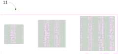
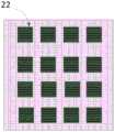
第一方面,为解决上述技术问题,本发明提供了一种焊盘结构,具体可以包括:多个主焊盘和位于每个所述主焊盘中的多个副焊盘;其中,所述多个主焊盘沿X方向或Y方向依次并排间隔排列,而位于每个主焊盘中的多个副焊盘则沿X方向和Y方向依次间隔对称排列。In the first aspect, in order to solve the above-mentioned technical problems, the present invention provides a pad structure, which may specifically include: a plurality of main pads and a plurality of sub-pads located in each of the main pads; wherein, the A plurality of main pads are arranged side by side in sequence along the X direction or a Y direction, and a plurality of sub pads located in each main pad are arranged symmetrically at intervals along the X direction and the Y direction.
进一步的,所述主焊盘可以为正四边形,所述主焊盘的边长范围可以为400μm~600μm。Further, the main pad may be a regular quadrilateral, and the side length of the main pad may range from 400 μm to 600 μm.
进一步的,所述副焊盘可以为正方向,所述副焊盘的边长范围可以为50μm~70μm。Further, the sub-pad can be in the forward direction, and the side length of the sub-pad can be in the range of 50 μm to 70 μm.
进一步的,多个所述主焊盘的尺寸可以相同,也可以不同,而多个所述副焊盘的尺寸均相同。Further, the sizes of the multiple main pads may be the same or different, and the sizes of the multiple sub-pads are all the same.
第二方面,基于如上所述的焊盘结构,本发明还提供了一种光刻拼接工艺的在线监控方法,具体可以包括如下步骤:In the second aspect, based on the pad structure as described above, the present invention also provides an online monitoring method for a photolithographic splicing process, which may specifically include the following steps:
确定拼接芯片版图,所述拼接芯片版图用于利用超级拼接工艺制造的包含超大像素单元的图像传感器,并基于所述权利要求1-3中任一项所述的焊盘结构,在所述拼接芯片版图中的拼接芯片的外围设置至少一个所述焊盘结构;Determine the splicing chip layout, the splicing chip layout is used for the image sensor containing super large pixel units manufactured by super splicing process, and based on the pad structure described in any one of claims 1-3, in the splicing At least one pad structure is arranged on the periphery of the spliced chip in the chip layout;
对包含所述焊盘结构的拼接芯片版图进行包括多次分区域曝光的光刻拼接工艺,以在目标晶圆上形成包含多个与所述拼接芯片版图相对应的拼接芯片的实际版图;performing a photolithographic splicing process including multiple sub-regional exposures on the spliced chip layout including the pad structure, so as to form an actual layout comprising a plurality of spliced chips corresponding to the spliced chip layout on the target wafer;
对所述拼接芯片的实际版图进行测量,以确定出所述拼接芯片的尺寸,并在对所述拼接芯片进行对准、划片后,找出预置焊盘结构,并利用该预置焊盘结构测量该拼接芯片的膜厚。Measure the actual layout of the spliced chip to determine the size of the spliced chip, and after aligning and scribing the spliced chip, find out the preset pad structure, and use the preset pad structure to determine the size of the spliced chip. The disk structure measures the film thickness of the stitched chip.
进一步的,所述目标晶圆所包含的拼接芯片的数目可以﹤16。Further, the number of splice chips contained in the target wafer may be <16.
进一步的,所述目标晶圆所包含的拼接芯片的数目具体可以为2。Further, the number of splice chips included in the target wafer may specifically be two.
进一步的,所述拼接芯片的实际版图尺寸具体可以大于26mm×33mm。Further, the actual layout size of the spliced chip may specifically be larger than 26mm×33mm.
进一步的,可以采用人工测量的方式确定所述拼接芯片的尺寸。Further, the size of the spliced chip can be determined by manual measurement.
进一步的,采用人工操作的方式对所述目标晶圆进行划片。Further, the target wafer is diced manually.
与现有技术相比,本发明技术方案至少存在如下有益效果之一:Compared with the prior art, the technical solution of the present invention has at least one of the following beneficial effects:
1、本发明提供了一种新型的焊盘结构,包括多个并排排列的大焊盘(主焊盘),以及内嵌在每个大焊盘(主焊盘)中的多个正方形的小焊盘(副焊盘),从而提出一种将大小焊盘嵌套的方式,形成一组用于全方位无死角对拼接芯片的某些参数进行测试的焊盘结构。1. The present invention provides a new type of pad structure, including multiple large pads (main pads) arranged side by side, and multiple small square pads embedded in each large pad (main pad). Welding pads (sub-pads), thus proposing a method of nesting large and small pads to form a set of pad structures for testing certain parameters of spliced chips in all directions without dead ends.
2、在基于本发明所提供的上述新型结构的焊盘结构后,本发明还提供了一种光刻拼接工艺的在线监控方法,以利用该特殊结构的焊盘结构,并结合人工测量芯片大小、人工划片等人工操作方式,进而解决现有技术中无法直接对利用超级拼接工艺制造的包含超大像素单元的图像传感器的版图中拼接芯片版图的厚度进行监控和测量的问题。2. After the pad structure based on the above-mentioned new structure provided by the present invention, the present invention also provides an online monitoring method for the photolithography splicing process, so as to use the pad structure of this special structure, combined with manual measurement of chip size , manual scribing and other manual operation methods, and then solve the problem in the prior art that it is impossible to directly monitor and measure the thickness of the spliced chip layout in the layout of the image sensor containing super large pixel units manufactured by the super splicing process.
附图说明Description of drawings
图1为本发明一实施例中的焊盘结构中主焊盘的结构示意图;FIG. 1 is a schematic structural diagram of a main pad in a pad structure in an embodiment of the present invention;
图2为本发明一实施例中的焊盘结构中任一主焊盘及其副焊盘的结构示意图;FIG. 2 is a structural schematic diagram of any main pad and its sub-pad in the pad structure in an embodiment of the present invention;
图3为本发明一实施例中的光刻拼接工艺的在线监控方法的流程示意图。FIG. 3 is a schematic flowchart of an online monitoring method for a photolithographic splicing process in an embodiment of the present invention.
具体实施方式Detailed ways
承如背景技术所述,为打破高端CIS产品被国外厂商所垄断的格局,近年来本领域研究人员主要致力于超高像素、超高帧速、全天候超高清的科学级应用CIS产品的研发,开创性得引入超级拼接工艺(将光罩拆分成多块曝光区域并分别在晶圆上多次曝光),成功制造出具有超大像素单元(7.5um)、超高像素(2.25亿像素)、超大面阵(>10um*10um)的CIS芯片,是目前世界上像素最高、面阵最大的产品,每片12英寸晶圆仅可制备2颗芯片。其中,拼接技术,顾名思义就是把在芯片的制造过程中,把涉及的图形分区,依次曝光,最终拼接成一个大尺寸的图形传感器。As mentioned in the background technology, in order to break the monopoly of high-end CIS products by foreign manufacturers, in recent years, researchers in this field have mainly devoted themselves to the research and development of scientific-level application CIS products with ultra-high pixel, ultra-high frame rate, and all-weather ultra-high definition. Groundbreakingly introduced the super splicing process (split the mask into multiple exposure areas and expose them multiple times on the wafer), and successfully manufactured a super-large pixel unit (7.5um), ultra-high pixel (225 million pixels), The super large area array (>10um*10um) CIS chip is currently the product with the highest pixel and the largest area array in the world. Each 12-inch wafer can only produce 2 chips. Among them, splicing technology, as the name implies, is to partition the involved graphics in the chip manufacturing process, expose them in sequence, and finally splice them into a large-size graphics sensor.
目前,对于传统的芯片,线上工艺可以正常通过monitorpad进行监控,recipe setup只需进行alignment然后画die,最后根据坐标找到量测pad,便可准确测量膜厚。但是,对于超级拼接工艺的拼接产品而言,由于wafer内有效芯片die数量远少于正常晶圆wafer中所包含的芯片die数量,进而导致无法划die,也即不能进行膜厚量测。At present, for traditional chips, the online process can be monitored normally through the monitorpad. The recipe setup only needs to perform alignment and then draw the die, and finally find the measurement pad according to the coordinates to accurately measure the film thickness. However, for the splicing products of the super splicing process, since the number of effective chip dies in the wafer is far less than the number of chip dies contained in the normal wafer wafer, it is impossible to scribe the die, that is, the film thickness measurement cannot be performed.
为此,本发明提供了一种焊盘结构及光刻拼接工艺的在线监控方法,以解决现有技术中无法直接对利用超级拼接工艺制造的包含超大像素单元的图像传感器的版图中拼接芯片版图的厚度进行监控和测量的问题。For this reason, the present invention provides an online monitoring method for a bonding pad structure and a photolithography splicing process, so as to solve the problem that in the prior art, it is impossible to directly splice the chip layout in the layout of an image sensor containing a super large pixel unit manufactured by a super splicing process. The thickness is monitored and measured.
以下结合附图和具体实施例对本发明提出的一种焊盘结构及光刻拼接工艺的在线监控方法作进一步详细说明。根据下面说明,本发明的优点和特征将更清楚。需说明的是,附图均采用非常简化的形式且均使用非精准的比例,仅用以方便、明晰地辅助说明本发明实施例的目的。在下面的描述中阐述了很多具体细节以便于充分理解本发明,但是本发明还可以采用其它不同于在此描述的其它方式来实施,因此本发明不受下面公开的具体实施例的限制。A bonding pad structure and an on-line monitoring method for a photolithographic splicing process proposed by the present invention will be further described in detail below with reference to the accompanying drawings and specific embodiments. The advantages and features of the present invention will become clearer from the following description. It should be noted that all the drawings are in a very simplified form and use imprecise scales, and are only used to facilitate and clearly assist the purpose of illustrating the embodiments of the present invention. In the following description, many specific details are set forth in order to fully understand the present invention, but the present invention can also be implemented in other ways than those described here, so the present invention is not limited by the specific embodiments disclosed below.
如本申请和权利要求书中所示,除非上下文明确提示例外情形,“一”、“一个”、“一种”和/或“该”等词并非特指单数,也可包括复数。一般说来,术语“包括”与“包含”仅提示包括已明确标识的步骤和元素,而这些步骤和元素不构成一个排它性的罗列,方法或者设备也可能包含其他的步骤或元素。在详述本发明实施例时,为便于说明,表示器件结构的剖面图会不依一般比例作局部放大,而且所述示意图只是示例,其在此不应限制本发明保护的范围。此外,在实际制作中应包含长度、宽度及深度的三维空间尺寸。As indicated in this application and claims, the terms "a", "an", "an" and/or "the" do not refer to the singular and may include the plural unless the context clearly indicates an exception. Generally speaking, the terms "comprising" and "comprising" only suggest the inclusion of clearly identified steps and elements, and these steps and elements do not constitute an exclusive list, and the method or device may also contain other steps or elements. When describing the embodiments of the present invention in detail, for the convenience of explanation, the cross-sectional view showing the device structure will not be partially enlarged according to the general scale, and the schematic diagram is only an example, which should not limit the protection scope of the present invention. In addition, the three-dimensional space dimensions of length, width and depth should be included in actual production.
下面首先对本发明实施例提供的焊盘结构进行介绍,具体参见图1和图2,其中,图1为本发明一实施例中的焊盘结构中主焊盘的结构示意图;In the following, the pad structure provided by the embodiment of the present invention is firstly introduced, referring to FIG. 1 and FIG. 2 for details, wherein FIG. 1 is a schematic structural diagram of the main pad in the pad structure in an embodiment of the present invention;
图2为本发明一实施例中的焊盘结构中任一主焊盘及其副焊盘的结构示意图。结合上述图1和图2可知,本发明提供的焊盘结构,具体可以包括:多个主焊盘11和位于每个所述主焊盘中的多个副焊盘22;其中,所述多个主焊盘11可以沿X方向或Y方向依次并排间隔排列,而位于每个主焊盘11中的多个副焊盘22则沿X方向和Y方向依次间隔对称排列。FIG. 2 is a schematic structural diagram of any main pad and its sub-pads in the pad structure according to an embodiment of the present invention. 1 and 2 above, it can be seen that the pad structure provided by the present invention may specifically include: multiple
作为一种示例,在本发明实施例中,所述主焊盘11的形状具体可以为正四边形,即,可以为如图1所述的正方形,而当所述主焊盘的形状为正方形时,其边长范围具体可以为400μm~600μm,即,本发明所提供的所述的主焊盘可以为边长为400μm的正方形,还可以是边长为500μm的正方形,还可以是边长为600μm的正方形,如图1所示。并且,示例性的,位于所述形状为正方形的所述主焊盘11内的多个副焊盘的图形均可以为正方向,而当所述副焊盘的形状为正方形时,其边长范围具体可以为为50μm~70μm,即,本发明所提供的所述的副焊盘可以为边长为50μm的正方形,还可以是边长为60μm的正方形,还可以是边长为70μm的正方形,如图2所示。As an example, in the embodiment of the present invention, the shape of the
在本实施例中,提供的所述新型的焊盘结构,其包括多个并排排列的大焊盘(主焊盘),以及内嵌在每个大焊盘(主焊盘)中的多个正方形的小焊盘(副焊盘),从而提出一种将大小焊盘嵌套的方式,形成一组用于全方位无死角对拼接芯片的某些参数进行测试的焊盘结构。In this embodiment, the novel pad structure provided includes a plurality of large pads (main pads) arranged side by side, and multiple pads embedded in each large pad (main pads). Square small pads (secondary pads), thus proposing a method of nesting large and small pads to form a set of pad structures for testing certain parameters of the spliced chip in all directions without dead ends.
需要说明的是,在本发明实施例中,其可以是如图1所述的三种不同尺寸的主焊盘沿一个方向,例如X方向或Y方向依次片排列,其在其他实施例中,还可以是相同尺寸的多个主焊盘沿一个方向,例如X方向或Y方向依次片排列。而不管主焊盘是上述哪种情况,本发明提供的内嵌在每一所述主焊盘中的多个副焊盘的尺寸是相同,且优选的尺寸为60μm*60μm的正方形。It should be noted that, in the embodiment of the present invention, it may be that the main pads of three different sizes as shown in FIG. 1 are arranged sequentially in one direction, such as the X direction or the Y direction. In other embodiments, It is also possible that a plurality of main pads of the same size are arranged sequentially in one direction, such as the X direction or the Y direction. No matter which of the main pads is the above situation, the multiple sub-pads embedded in each of the main pads provided by the present invention have the same size, and the preferred size is a square of 60 μm*60 μm.
基于上述图1所述的焊盘结构,本发明实施例中还提供了一种光刻拼接工艺的在线监控方法。具体参见图3,图3为本发明提供的一种光刻拼接工艺的在线监控方法的流程示意图。所述光刻拼接工艺的在线监控方法,具体包括如下步骤:Based on the pad structure described above in FIG. 1 , an embodiment of the present invention also provides an online monitoring method for a photolithographic splicing process. Referring to FIG. 3 for details, FIG. 3 is a schematic flowchart of an online monitoring method for a photolithographic splicing process provided by the present invention. The on-line monitoring method of the photolithographic splicing process specifically includes the following steps:
步骤S100,确定拼接芯片版图,所述拼接芯片版图用于利用超级拼接工艺制造的包含超大像素单元的图像传感器,并基于如上所述的焊盘结构,在所述拼接芯片版图中的拼接芯片的外围设置至少一个所述焊盘结构。其中,所述拼接芯片的实际版图尺寸大于26mm×33mm。Step S100, determine the layout of the spliced chip, the layout of the spliced chip is used for the image sensor containing super large pixel units manufactured by the super splicing process, and based on the above-mentioned pad structure, the spliced chip in the spliced chip layout At least one pad structure is arranged on the periphery. Wherein, the actual layout size of the spliced chip is larger than 26mm×33mm.
在本实施例中,当芯片尺寸超过芯片版图最大曝光尺寸26mm×33mm时,将无法通过常规的单步光刻工艺来获得,此时便需要通过多次分区域光刻拼接工艺(即分区曝光并进行图案拼接)来实现。具体的,可以根据本发明实施提供的拼接芯片版图的设计方式,设计大尺寸芯片的拼接芯片版图;然后,在通过光刻工艺,以所述设计的拼接芯片版图为掩膜版,对目标晶圆进行多次,分区域曝光,从而在目标晶圆上形成拼接芯片的实际版图。在所述光刻拼接工艺中,位于所述拼接芯片版图的同一主遮光带两侧的套刻对准标志一一对应地套准在一起,以使得所述拼接芯片的实际版图在相应的位置形成相应的套刻对准标志的拼缝。In this embodiment, when the chip size exceeds the maximum exposure size of the chip layout of 26mm×33mm, it cannot be obtained through the conventional single-step photolithography process. And pattern splicing) to achieve. Specifically, according to the design method of the spliced chip layout provided by the implementation of the present invention, the spliced chip layout of the large-size chip can be designed; The circle is exposed multiple times, and the exposure is divided into regions, so as to form the actual layout of the spliced chip on the target wafer. In the photolithographic splicing process, the overlay alignment marks located on both sides of the same main shading zone of the spliced chip layout are registered together one by one, so that the actual layout of the spliced chip is in the corresponding position Form a patchwork of corresponding overlay alignment marks.
而在本实施例中,由于发明人为了得到超高像素、超高帧速、全天候超高清的科学级应用CIS产品的研发,其开创性得引入超级拼接工艺(将光罩拆分成多块曝光区域并分别在晶圆上多次曝光),成功制造出具有超大像素单元(7.5um)、超高像素(2.25亿像素)、超大面阵(>10um*10um)的CIS芯片,是目前世界上像素最高、面阵最大的产品。但是这种芯片产品中的每片12英寸晶圆仅可制备2颗芯片。而由于wafer内有效芯片die数量远少于正常晶圆wafer中所包含的芯片die数量,进而导致无法划die,也即不能进行膜厚量测。In this embodiment, because the inventor has pioneered the introduction of a super splicing process (splitting the mask into multiple pieces) in order to obtain super-high pixel, super-high frame rate, and all-weather ultra-high-definition scientific application CIS product research and development. exposure area and multiple exposures on the wafer), and successfully manufactured CIS chips with super large pixel units (7.5um), super high pixels (225 million pixels), and super large area arrays (>10um*10um). The product with the highest pixels and the largest area array. But each 12-inch wafer in this chip product can only produce 2 chips. However, since the number of effective chip dies in the wafer is far less than the number of chip dies contained in the normal wafer wafer, it is impossible to scribe the die, that is, it is impossible to measure the film thickness.
为此,本发明发明提出了一种利用如图1、图2所示的新型焊盘结构进行膜厚量测的方法,然后,利用该特殊结构的焊盘结构,并结合人工测量芯片大小、人工划片等人工操作方式,进而解决现有技术中无法直接对利用超级拼接工艺制造的包含超大像素单元的图像传感器的版图中拼接芯片版图的厚度进行监控和测量的问题。For this reason, the present invention proposes a kind of method that utilizes the novel pad structure as shown in Figure 1, Figure 2 to carry out film thickness measurement, then, utilizes the pad structure of this special structure, and combines manual measurement chip size, Manual scribing and other manual operations can further solve the problem in the prior art that it is impossible to directly monitor and measure the thickness of the spliced chip layout in the layout of the image sensor containing super large pixel units manufactured by the super splicing process.
步骤S200,对包含所述焊盘结构的拼接芯片版图进行包括多次分区域曝光的光刻拼接工艺,以在目标晶圆上形成包含多个与所述拼接芯片版图相对应的拼接芯片的实际版图。其中,所述目标晶圆所包含的拼接芯片的数目﹤16,而在本发明实施例中,所述目标晶圆所包含的拼接芯片的数目为2。Step S200, performing a photolithography splicing process including multiple sub-regional exposures on the spliced chip layout including the pad structure, so as to form a real spliced chip that includes multiple spliced chips corresponding to the spliced chip layout on the target wafer. territory. Wherein, the number of spliced chips included in the target wafer is <16, and in the embodiment of the present invention, the number of spliced chips included in the target wafer is 2.
步骤S300,对所述拼接芯片的实际版图进行测量,以确定出所述拼接芯片的尺寸,并在对所述拼接芯片进行对准、划片后,找出预置焊盘结构,并利用该预置焊盘结构测量该拼接芯片的膜厚。Step S300, measure the actual layout of the spliced chip to determine the size of the spliced chip, and after aligning and dicing the spliced chip, find out the preset pad structure, and use the The pre-pad structure measures the film thickness of the spliced chip.
在本实施例中,本发明人提出了一种可以先采用人工测量的方式确定所述拼接芯片的尺寸,之后在采用人工操作的方式对所述目标晶圆进行划片,最后再找到指定用于两侧拼接芯片的膜厚的一个或多个所述焊盘,然后利用该焊盘进行量测,以对应确定出待测试的参数。In this embodiment, the inventor proposes a method that can first determine the size of the spliced chip by manual measurement, then use manual operation to scribe the target wafer, and finally find the specified wafer. Splicing one or more pads of the film thickness of the chip on both sides, and then use the pads to measure, so as to determine the parameters to be tested correspondingly.
综上所述,本发明提供了一种新型的焊盘结构,包括多个并排排列的大焊盘(主焊盘),以及内嵌在每个大焊盘(主焊盘)中的多个正方形的小焊盘(副焊盘),从而提出一种将大小焊盘嵌套的方式,形成一组用于全方位无死角对拼接芯片的某些参数进行测试的焊盘结构。In summary, the present invention provides a novel pad structure, including a plurality of large pads (main pads) arranged side by side, and a plurality of pads embedded in each large pad (main pads). Square small pads (secondary pads), thus proposing a method of nesting large and small pads to form a set of pad structures for testing certain parameters of the spliced chip in all directions without dead ends.
进一步的,在基于本发明所提供的上述新型结构的焊盘结构后,本发明还提供了一种光刻拼接工艺的在线监控方法,以利用该特殊结构的焊盘结构,并结合人工测量芯片大小、人工划片等人工操作方式,进而解决现有技术中无法直接对利用超级拼接工艺制造的包含超大像素单元的图像传感器的版图中拼接芯片版图的厚度进行监控和测量的问题。Furthermore, based on the pad structure of the above-mentioned new structure provided by the present invention, the present invention also provides an online monitoring method for the photolithographic splicing process, so as to use the pad structure of this special structure and combine the manual measurement of the chip Size, manual scribing and other manual operation methods, and then solve the problem in the prior art that it is impossible to directly monitor and measure the thickness of the spliced chip layout in the layout of the image sensor containing super large pixel units manufactured by the super splicing process.
需要说明的是,本发明实施例还提供了一种电子设备,包括处理器、通信接口、存储器和通信总线,其中,处理器,通信接口,存储器通过通信总线完成相互间的通信,It should be noted that an embodiment of the present invention also provides an electronic device, including a processor, a communication interface, a memory, and a communication bus, wherein the processor, the communication interface, and the memory complete communication with each other through the communication bus,
存储器,用于存放计算机程序;memory for storing computer programs;
处理器,用于执行存储器上所存放的程序时,实现本发明实施例提供的一种光刻拼接工艺的在线监控方法。The processor is configured to implement an online monitoring method for a photolithographic splicing process provided by an embodiment of the present invention when executing a program stored in the memory.
另外,处理器执行存储器上所存放的程序而实现的光刻拼接工艺的在线监控方法的其他实现方式,与前述方法实施例部分所提及的实现方式相同,这里也不再赘述。In addition, other implementations of the online monitoring method of the lithography splicing process realized by the processor executing the program stored in the memory are the same as those mentioned in the foregoing method embodiments, and will not be repeated here.
上述控制终端提到的通信总线可以是外设部件互连标准(Peripheral ComponentInterconnect,PCI)总线或扩展工业标准结构(Extended IndustryStandardArchitecture,EISA)总线等。该通信总线可以分为地址总线、数据总线、控制总线等。为便于表示,图中仅用一条粗线表示,但并不表示仅有一根总线或一种类型的总线。The communication bus mentioned above by the control terminal may be a Peripheral Component Interconnect (PCI) bus or an Extended Industry Standard Architecture (EISA) bus or the like. The communication bus can be divided into an address bus, a data bus, a control bus, and the like. For ease of representation, only one thick line is used in the figure, but it does not mean that there is only one bus or one type of bus.
通信接口用于上述电子设备与其他设备之间的通信。The communication interface is used for communication between the electronic device and other devices.
存储器可以包括随机存取存储器(RandomAccess Memory,RAM),也可以包括非易失性存储器(Non-Volatile Memory,NVM),例如至少一个磁盘存储器。可选的,存储器还可以是至少一个位于远离前述处理器的存储装置。The memory may include a random access memory (Random Access Memory, RAM), and may also include a non-volatile memory (Non-Volatile Memory, NVM), such as at least one magnetic disk memory. Optionally, the memory may also be at least one storage device located far away from the aforementioned processor.
上述的处理器可以是通用处理器,包括中央处理器(Central Processing Unit,CPU)、网络处理器(Network Processor,NP)等;还可以是数字信号处理器(Digital SignalProcessing,DSP)、专用集成电路(Application Specific Integrated Circuit,ASIC)、现场可编程门阵列(Field-Programmable GateArray,FPGA)或者其他可编程逻辑器件、分立门或者晶体管逻辑器件、分立硬件组件。The above-mentioned processor can be a general-purpose processor, including a central processing unit (Central Processing Unit, CPU), a network processor (Network Processor, NP), etc.; it can also be a digital signal processor (Digital Signal Processing, DSP), an application-specific integrated circuit (Application Specific Integrated Circuit, ASIC), Field-Programmable Gate Array (Field-Programmable GateArray, FPGA) or other programmable logic devices, discrete gate or transistor logic devices, discrete hardware components.
在本发明提供的又一实施例中,还提供了一种计算机可读存储介质,该计算机可读存储介质中存储有指令,当其在计算机上运行时,使得计算机执行上述实施例中任一所述的光刻拼接工艺的在线监控方法。In yet another embodiment provided by the present invention, a computer-readable storage medium is also provided. Instructions are stored in the computer-readable storage medium. When the computer-readable storage medium is run on a computer, it causes the computer to execute any one of the above-mentioned embodiments. The online monitoring method of the photolithographic splicing process.
在上述实施例中,可以全部或部分地通过软件、硬件、固件或者其任意组合来实现。当使用软件实现时,可以全部或部分地以计算机程序产品的形式实现。所述计算机程序产品包括一个或多个计算机指令。在计算机上加载和执行所述计算机程序指令时,全部或部分地产生按照本发明实施例所述的流程或功能。所述计算机可以是通用计算机、专用计算机、计算机网络、或者其他可编程装置。所述计算机指令可以存储在计算机可读存储介质中,或者从一个计算机可读存储介质向另一个计算机可读存储介质传输,例如,所述计算机指令可以从一个网站站点、计算机、服务器或数据中心通过有线(例如同轴电缆、光纤、数字用户线(DSL))或无线(例如红外、无线、微波等)方式向另一个网站站点、计算机、服务器或数据中心进行传输。所述计算机可读存储介质可以是计算机能够存取的任何可用介质或者是包含一个或多个可用介质集成的服务器、数据中心等数据存储设备。所述可用介质可以是磁性介质,(例如,软盘、硬盘、磁带)、光介质(例如,DVD)、或者半导体介质(例如固态硬盘Solid State Disk(SSD))等。In the above embodiments, all or part of them may be implemented by software, hardware, firmware or any combination thereof. When implemented using software, it may be implemented in whole or in part in the form of a computer program product. The computer program product includes one or more computer instructions. When the computer program instructions are loaded and executed on the computer, all or part of the processes or functions according to the embodiments of the present invention will be generated. The computer can be a general purpose computer, a special purpose computer, a computer network, or other programmable devices. The computer instructions may be stored in or transmitted from one computer-readable storage medium to another computer-readable storage medium, for example, the computer instructions may be transmitted from a website, computer, server or data center Transmission to another website site, computer, server, or data center by wired (eg, coaxial cable, optical fiber, digital subscriber line (DSL)) or wireless (eg, infrared, wireless, microwave, etc.). The computer-readable storage medium may be any available medium that can be accessed by a computer, or a data storage device such as a server or a data center integrated with one or more available media. The available medium may be a magnetic medium (such as a floppy disk, a hard disk, or a magnetic tape), an optical medium (such as a DVD), or a semiconductor medium (such as a Solid State Disk (SSD)).
需要说明的是,在本文中,诸如第一和第二等之类的关系术语仅仅用来将一个实体或者操作与另一个实体或操作区分开来,而不一定要求或者暗示这些实体或操作之间存在任何这种实际的关系或者顺序。而且,术语“包括”、“包含”或者其任何其他变体意在涵盖非排他性的包含,从而使得包括一系列要素的过程、方法、物品或者设备不仅包括那些要素,而且还包括没有明确列出的其他要素,或者是还包括为这种过程、方法、物品或者设备所固有的要素。在没有更多限制的情况下,由语句“包括一个……”限定的要素,并不排除在包括所述要素的过程、方法、物品或者设备中还存在另外的相同要素。It should be noted that in this article, relational terms such as first and second are only used to distinguish one entity or operation from another entity or operation, and do not necessarily require or imply that there is a relationship between these entities or operations. There is no such actual relationship or order between them. Furthermore, the term "comprises", "comprises" or any other variation thereof is intended to cover a non-exclusive inclusion such that a process, method, article, or apparatus comprising a set of elements includes not only those elements, but also includes elements not expressly listed. other elements of or also include elements inherent in such a process, method, article, or device. Without further limitations, an element defined by the phrase "comprising a ..." does not exclude the presence of additional identical elements in the process, method, article or apparatus comprising said element.
本说明书中的各个实施例均采用相关的方式描述,各个实施例之间相同相似的部分互相参见即可,每个实施例重点说明的都是与其他实施例的不同之处。尤其,对于装置、电子设备以及计算机可读存储介质实施例而言,由于其基本相似于方法实施例,所以描述的比较简单,相关之处参见方法实施例的部分说明即可。Each embodiment in this specification is described in a related manner, the same and similar parts of each embodiment can be referred to each other, and each embodiment focuses on the differences from other embodiments. In particular, for the apparatus, electronic equipment, and computer-readable storage medium embodiments, since they are basically similar to the method embodiments, the description is relatively simple, and for relevant parts, refer to part of the description of the method embodiments.
以上所述仅为本发明的较佳实施例而已,并非用于限定本发明的保护范围。凡在本发明的精神和原则之内所作的任何修改、等同替换、改进等,均包含在本发明的保护范围内。The above descriptions are only preferred embodiments of the present invention, and are not intended to limit the protection scope of the present invention. Any modification, equivalent replacement, improvement, etc. made within the spirit and principles of the present invention are included in the protection scope of the present invention.
Claims (10)
Translated fromChinesePriority Applications (1)
| Application Number | Priority Date | Filing Date | Title |
|---|---|---|---|
| CN202211420247.XACN115910825A (en) | 2022-11-15 | 2022-11-15 | On-line monitoring method of pad structure and photolithography splicing process |
Applications Claiming Priority (1)
| Application Number | Priority Date | Filing Date | Title |
|---|---|---|---|
| CN202211420247.XACN115910825A (en) | 2022-11-15 | 2022-11-15 | On-line monitoring method of pad structure and photolithography splicing process |
Publications (1)
| Publication Number | Publication Date |
|---|---|
| CN115910825Atrue CN115910825A (en) | 2023-04-04 |
Family
ID=86489037
Family Applications (1)
| Application Number | Title | Priority Date | Filing Date |
|---|---|---|---|
| CN202211420247.XAPendingCN115910825A (en) | 2022-11-15 | 2022-11-15 | On-line monitoring method of pad structure and photolithography splicing process |
Country Status (1)
| Country | Link |
|---|---|
| CN (1) | CN115910825A (en) |
Citations (6)
| Publication number | Priority date | Publication date | Assignee | Title |
|---|---|---|---|---|
| CN103545324A (en)* | 2012-07-12 | 2014-01-29 | 台湾积体电路制造股份有限公司 | Method and apparatus for image sensor packaging |
| CN110391147A (en)* | 2019-07-26 | 2019-10-29 | 德淮半导体有限公司 | Pad structure and method of forming the same |
| CN110660815A (en)* | 2018-06-28 | 2020-01-07 | 格科微电子(上海)有限公司 | Design Method of CMOS Image Sensor Wafer |
| CN112180691A (en)* | 2020-09-30 | 2021-01-05 | 上海华力集成电路制造有限公司 | On-line monitoring method for spliced chips |
| CN112540507A (en)* | 2020-12-16 | 2021-03-23 | 上海华力微电子有限公司 | Overlay precision monitoring method for splicing chip layout and photoetching splicing process |
| CN113097135A (en)* | 2019-12-23 | 2021-07-09 | 格科微电子(上海)有限公司 | Method for improving wafer cutting performance and wafer structure |
- 2022
- 2022-11-15CNCN202211420247.XApatent/CN115910825A/enactivePending
Patent Citations (6)
| Publication number | Priority date | Publication date | Assignee | Title |
|---|---|---|---|---|
| CN103545324A (en)* | 2012-07-12 | 2014-01-29 | 台湾积体电路制造股份有限公司 | Method and apparatus for image sensor packaging |
| CN110660815A (en)* | 2018-06-28 | 2020-01-07 | 格科微电子(上海)有限公司 | Design Method of CMOS Image Sensor Wafer |
| CN110391147A (en)* | 2019-07-26 | 2019-10-29 | 德淮半导体有限公司 | Pad structure and method of forming the same |
| CN113097135A (en)* | 2019-12-23 | 2021-07-09 | 格科微电子(上海)有限公司 | Method for improving wafer cutting performance and wafer structure |
| CN112180691A (en)* | 2020-09-30 | 2021-01-05 | 上海华力集成电路制造有限公司 | On-line monitoring method for spliced chips |
| CN112540507A (en)* | 2020-12-16 | 2021-03-23 | 上海华力微电子有限公司 | Overlay precision monitoring method for splicing chip layout and photoetching splicing process |
Similar Documents
| Publication | Publication Date | Title |
|---|---|---|
| TWI784018B (en) | Systems and methods for predicting defects and critical dimension using deep learning in the semiconductor manufacturing process | |
| TWI524079B (en) | Inspection method for contact by die to database | |
| JP4943616B2 (en) | Straight line defect detection | |
| TWI552245B (en) | Methodology of incorporating wafer physical measurement with digital simulation for improving semiconductor device fabrication | |
| WO2021244231A1 (en) | Design method for wafer layout and lithography machine exposure system | |
| CN103676490A (en) | Method for monitoring weak point forming reasons | |
| CN103454852A (en) | Mask and overlay precision measuring method | |
| TWI807442B (en) | In-die metrology methods and systems for process control | |
| CN107452717B (en) | Semiconductor making method | |
| CN112180691B (en) | On-line monitoring method for spliced chip | |
| CN102944983A (en) | Method for improving key dimension measurement of pattern to be measured | |
| CN115910825A (en) | On-line monitoring method of pad structure and photolithography splicing process | |
| TWI809830B (en) | Method of determining overlay error during semiconductor fabrication | |
| Tian et al. | Critical defect detection, monitoring and fix through process integration engineering by using D2DB pattern monitor solution | |
| CN101561633A (en) | Method for monitoring photoetching process and monitoring mark | |
| CN106154755A (en) | The detection method of photoresist thickness abnormity | |
| TWI432915B (en) | Method for monitoring photolithography process and monitor mark | |
| CN107783369B (en) | Optical proximity correction repairing method | |
| CN116613142A (en) | Method for determining overlay error during semiconductor fabrication | |
| CN116190258A (en) | Failure positioning method and electronic equipment | |
| CN108369920B (en) | Adaptive alignment method and system | |
| CN103488044A (en) | Mask pattern analysis device and mask pattern analysis method | |
| CN103837105B (en) | The measuring method of critical size | |
| TW556294B (en) | Semiconductor device | |
| CN110263438A (en) | Integrated circuit layout acute angle restorative procedure and integrated circuit layout acute angle repair system |
Legal Events
| Date | Code | Title | Description |
|---|---|---|---|
| PB01 | Publication | ||
| PB01 | Publication | ||
| SE01 | Entry into force of request for substantive examination | ||
| SE01 | Entry into force of request for substantive examination |