CN115903295A - LCD panel - Google Patents
LCD panelDownload PDFInfo
- Publication number
- CN115903295A CN115903295ACN202110931676.2ACN202110931676ACN115903295ACN 115903295 ACN115903295 ACN 115903295ACN 202110931676 ACN202110931676 ACN 202110931676ACN 115903295 ACN115903295 ACN 115903295A
- Authority
- CN
- China
- Prior art keywords
- liquid crystal
- display area
- substrate
- crystal display
- electrode layer
- Prior art date
- Legal status (The legal status is an assumption and is not a legal conclusion. Google has not performed a legal analysis and makes no representation as to the accuracy of the status listed.)
- Pending
Links
- 239000004973liquid crystal related substanceSubstances0.000claimsabstractdescription204
- 239000000758substrateSubstances0.000claimsabstractdescription67
- 239000000463materialSubstances0.000claimsabstractdescription48
- 238000007789sealingMethods0.000claimsabstractdescription14
- 239000004983Polymer Dispersed Liquid CrystalSubstances0.000claimsdescription9
- 229920000642polymerPolymers0.000claimsdescription5
- 238000010586diagramMethods0.000description11
- 229920000106Liquid crystal polymerPolymers0.000description4
- 230000000007visual effectEffects0.000description3
- 230000000694effectsEffects0.000description2
- 230000001364causal effectEffects0.000description1
- 238000000034methodMethods0.000description1
Images


Landscapes
- Liquid Crystal (AREA)
Abstract
Description
Translated fromChinese技术领域technical field
本发明涉及一种液晶面板。The invention relates to a liquid crystal panel.
背景技术Background technique
现有的移动设备具备自拍摄像头。为了不影响自拍摄像头的摄像效果,目前自拍摄像头是以通孔设计或盲孔设计的方式来布置于移动设备的液晶面板中,且自拍摄像头的区域不用以显示。然而,此举占用了液晶面板的可显示区域,并造成较差的视觉效果。Existing mobile devices have selfie cameras. In order not to affect the camera effect of the selfie camera, currently the selfie camera is arranged in the liquid crystal panel of the mobile device in a through hole design or a blind hole design, and the area of the selfie camera is not used for display. However, this takes up the displayable area of the LCD panel and causes poor visual effects.
发明内容Contents of the invention
本发明的主要目的在于提供一种液晶面板,其显示液晶层包括第一液晶显示区以及第二液晶显示区,且第二液晶显示区的垂直投影与摄像头模块区的垂直投影彼此至少部分重迭,借由第二液晶显示区增加液晶面板的可显示区域。The main object of the present invention is to provide a liquid crystal panel, the display liquid crystal layer includes a first liquid crystal display area and a second liquid crystal display area, and the vertical projection of the second liquid crystal display area and the vertical projection of the camera module area at least partially overlap each other , increasing the displayable area of the liquid crystal panel by means of the second liquid crystal display area.
根据上述目的,本发明提出一种液晶面板,其包括第一基板、第二基板、显示液晶层以及摄像头模块区。显示液晶层包括第一液晶显示区、第二液晶显示区以及密封层。第一液晶显示区具有第一液晶材料。第二液晶显示区沿第一方向与第一液晶显示区相邻,并具有第二液晶材料,且第二液晶材料与第一液晶材料相异。密封层设于第一液晶显示区与第二液晶显示区之间。摄像头模块区设于第一基板之上。第二液晶显示区沿第二方向的垂直投影与摄像头模块区的垂直投影彼此至少部分重迭,且第二方向垂直于第一方向。According to the above purpose, the present invention provides a liquid crystal panel, which includes a first substrate, a second substrate, a display liquid crystal layer and a camera module area. The display liquid crystal layer includes a first liquid crystal display area, a second liquid crystal display area and a sealing layer. The first liquid crystal display area has a first liquid crystal material. The second liquid crystal display area is adjacent to the first liquid crystal display area along the first direction, and has a second liquid crystal material, and the second liquid crystal material is different from the first liquid crystal material. The sealing layer is arranged between the first liquid crystal display area and the second liquid crystal display area. The camera module area is disposed on the first substrate. The vertical projection of the second liquid crystal display area along the second direction and the vertical projection of the camera module area at least partially overlap with each other, and the second direction is perpendicular to the first direction.
根据上述目的,本发明另提出一种液晶面板,其包括第一基板、第二基板、第三基板、显示液晶层以及摄像头模块。显示液晶层包括第一液晶显示区、第二液晶显示区以及密封层。第一液晶显示区具有第一液晶材料。第二液晶显示区沿第一方向与第一液晶显示区相邻,并具有第二液晶材料,且第二液晶材料与第一液晶材料相异。密封层设于第一液晶显示区与第二液晶显示区之间。摄像头模块设于第三基板之上,且位于第一基板以及第三基板之间。第二液晶显示区沿第二方向的垂直投影与摄像头模块的垂直投影彼此至少部分重迭,且第二方向垂直于第一方向。According to the above purpose, the present invention further provides a liquid crystal panel, which includes a first substrate, a second substrate, a third substrate, a display liquid crystal layer, and a camera module. The display liquid crystal layer includes a first liquid crystal display area, a second liquid crystal display area and a sealing layer. The first liquid crystal display area has a first liquid crystal material. The second liquid crystal display area is adjacent to the first liquid crystal display area along the first direction, and has a second liquid crystal material, and the second liquid crystal material is different from the first liquid crystal material. The sealing layer is arranged between the first liquid crystal display area and the second liquid crystal display area. The camera module is disposed on the third substrate and located between the first substrate and the third substrate. The vertical projection of the second liquid crystal display area along the second direction and the vertical projection of the camera module at least partially overlap each other, and the second direction is perpendicular to the first direction.
根据本发明的又一实施例,第二液晶材料为聚合物分散液晶或聚合物网络液晶。According to yet another embodiment of the present invention, the second liquid crystal material is a polymer dispersed liquid crystal or a polymer network liquid crystal.
由上述构造,第二液晶显示区可增加液晶面板的可显示区域。With the above structure, the second liquid crystal display area can increase the displayable area of the liquid crystal panel.
为使能更进一步了解本发明的特征及技术内容,请参阅以下有关本发明的详细说明与附图,但是此等说明与所附图式仅系用来说明本发明,而非对本发明的权利范围作任何的限制。In order to enable a further understanding of the features and technical content of the present invention, please refer to the following detailed description and accompanying drawings of the present invention, but these descriptions and accompanying drawings are only used to illustrate the present invention, rather than to claim the rights of the present invention any limitations on the scope.
附图说明Description of drawings
为了更清楚地说明本发明实施例或现有技术中的技术方案,下面将对实施例描述中所需要使用的附图作简单地介绍,显而易见地,下面描述中的附图仅仅是本发明的一些实施例,对于本领域普通技术人员来讲,在不付出创造性劳动性的前提下,还可以根据这些附图获得其他的附图。In order to more clearly illustrate the embodiments of the present invention or the technical solutions in the prior art, the following will briefly introduce the accompanying drawings that need to be used in the description of the embodiments. Obviously, the accompanying drawings in the following description are only of the present invention. For some embodiments, those of ordinary skill in the art can also obtain other drawings based on these drawings without paying creative efforts.
图1是本发明的实施例的俯视图;Fig. 1 is the top view of the embodiment of the present invention;
图2是图1沿A-A’切割线的剖面图;Fig. 2 is the sectional view of Fig. 1 along A-A ' cutting line;
图3A是本发明的实施例的运作状态示意图一;FIG. 3A is a schematic diagram of the first operating state of an embodiment of the present invention;
图3B是本发明的实施例的运作状态示意图二;FIG. 3B is a second schematic diagram of the operating state of the embodiment of the present invention;
图3C是本发明的实施例的运作状态示意图三;FIG. 3C is a schematic diagram of the third operating state of the embodiment of the present invention;
图4是本发明的另一实施例的俯视图;Figure 4 is a top view of another embodiment of the present invention;
图5是图4沿B-B’切割线的剖面图;Fig. 5 is the sectional view of Fig. 4 along B-B ' cutting line;
图6A是本发明的另一实施例的运作状态示意图一;FIG. 6A is a schematic diagram of the first operating state of another embodiment of the present invention;
图6B是本发明的另一实施例的运作状态示意图二。FIG. 6B is a second schematic view of the operating state of another embodiment of the present invention.
【附图标记】[reference sign]
100 第一基板100 first substrate
200 第二基板200 second substrate
300 显示液晶层300 display liquid crystal layer
310 第一液晶显示区310 The first liquid crystal display area
311 电极层311 electrode layer
312 滤光层312 filter layer
313 第一液晶材料313 The first liquid crystal material
320 第二液晶显示区320 second liquid crystal display area
321 第一电极层321 first electrode layer
322 第二电极层322 second electrode layer
323 第二液晶材料323 second liquid crystal material
330 密封层330 sealing layer
400 摄像头模块区400 camera module area
500 摄像头模块500 camera modules
600 第三基板600 third substrate
1000、1000’ 液晶面板1000, 1000’ LCD panel
X 第一方向X first direction
Y 第二方向Y Second direction
具体实施方式Detailed ways
以下仔细讨论本发明的实施例。然而,可以理解的是,实施例提供许多可应用的概念,其可实施于各式各样的特定内容中。所讨论、揭示的实施例仅供说明,并非用以限定本发明的范围。Embodiments of the invention are discussed in detail below. It should be appreciated, however, that the embodiments provide many applicable concepts that can be implemented in a wide variety of specific contexts. The discussed and disclosed embodiments are for illustration only, and are not intended to limit the scope of the present invention.
可被理解的是,虽然在本文可使用“第一”、“第二”等用语来描述各种元件、零件、区域和/或部分,但这些用语不应限制这些元件、零件、区域和/或部分。这些用语仅用以区别一个元件、零件、区域和/或部分与另一个元件、零件、区域和/或部分。It can be understood that although terms such as “first” and “second” may be used herein to describe various elements, parts, regions and/or sections, these terms should not limit these elements, parts, regions and/or sections or part. These terms are only used to distinguish one element, component, region and/or section from another element, component, region and/or section.
在本文中所使用的用语仅是为了描述特定实施例,非用以限制权利要求。除非另有限制,否则单数形式的“一”或“该”用语也可用来表示复数形式。此外,在本文中可能会使用空间相对用语,例如“上方”、“上”、“下方”等等,以方便说明如附图所绘示的一个元件或一个特征与另一个元件或特征的关系。除了在附图中所绘示的方向外,这些空间相对性用语的使用是为了说明元件在使用或操作时的不同方位,而不只限于附图所绘示的方向。元件也可以其他方式定向(旋转90度或在其他方向),而在此使用的空间相对性描述也可以相同方式解读。The terminology used herein is for describing particular embodiments only, not for limiting the claims. The terms "a" or "the" in the singular may also be used in the plural unless limited otherwise. In addition, spatially relative terms, such as "above", "on", "below", etc., may be used herein to facilitate description of the relationship between one element or a feature and another element or feature as depicted in the drawings . In addition to the directions shown in the drawings, the use of these spatially relative terms is to describe different orientations of the components during use or operation, and is not limited to the directions shown in the drawings. Elements could be otherwise oriented (rotated 90 degrees or at other orientations), and the spatially relative descriptions used herein should be interpreted in the same way.
为了简化和明确说明,本文可能会在各种实施例中重复使用元件符号和/或字母,但这并不表示所讨论的各种实施例及/或配置之间有因果关系。For the sake of simplicity and clear description, element symbols and/or letters may be used repeatedly in various embodiments herein, but this does not mean that there is a causal relationship between the various embodiments and/or configurations discussed.
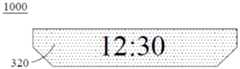
图1为本发明实施例的液晶面板1000的俯视图,其至少包括第一液晶显示区310、第二液晶显示区320以及摄像头模块区400。第二液晶显示区320至少部份覆盖摄像头模块区400。第二液晶显示区320以及摄像头模块区400位于液晶面板1000的凹口(notch)。FIG. 1 is a top view of a
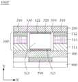
图2为图1的液晶面板1000沿A-A’切割线的剖面图。如图2所示,液晶面板1000包括第一基板100、第二基板200、显示液晶层300以及摄像头模块区400。显示液晶层300设于第一基板100与第二基板200之间。摄像头模块区400设于第一基板100之上并远离显示液晶层300,即摄像头模块区400与显示液晶层300设于第一基板100的不同侧。FIG. 2 is a cross-sectional view of the
显示液晶层300包括第一液晶显示区310、第二液晶显示区320以及密封层330,且第一液晶显示区310设于第二液晶显示区320的周围。第一液晶显示区310包括电极层311、滤光层312以及第一液晶材料313。电极层311设于第一基板100之上。滤光层312设于第二基板之上。第一液晶材料313设于电极层311与滤光层312之间。第二液晶显示区320包括第一电极层321、第二电极层322以及第二液晶材料323,且第二液晶显示区320沿第一方向X与第一液晶显示区310相邻,并第二液晶显示区320沿第二方向Y的垂直投影与摄像头模块区400的垂直投影至少部分重迭,且第二方向Y垂直于第一方向X。第一电极层321设于第一基板100之上。第二电极层322设于第二基板200之上。第二液晶材料323设于第一电极层321与第二电极层322之间,且第二液晶材料323与第一液晶材料313相异。密封层330设于第一基板100以及第二基板200之间,且位于第一液晶显示区310与第二液晶显示区320之间,并沿第一方向X环绕第二液晶材料323。The display
第一基板100以及第二基板200为透明基板。电极层311、第一电极层321以及第二电极层322为透明电极层。第二液晶材料323为聚合物分散液晶(Polymer DispersedLiquid Crystal,PDLC)或聚合物网络液晶(Polymer Network Liquid Crystal,PNLC)。摄像头模块区400至少包括摄像头元件。The
图3A至图3C为本发明之第二液晶显示区320之运作状态示意图。图3A为第二液晶显示区320为透明状态之示意图,因此摄像头模块区400不被第二液晶显示区320所遮蔽,摄像头模块区400可正常进行拍摄。图3B为第二液晶显示区320为雾化状态之示意图,因此摄像头模块区400被第二液晶显示区320所遮蔽,借此,除了提升液晶面板1000的视觉美观效果外,更可避免摄像头误动作而进行非期望的拍摄运作。图3C为第二液晶显示区320为显示状态之示意图,摄像头模块区400被第二液晶显示区320所遮蔽,同时部分的第二液晶显示区320用以显示提示资讯。3A to 3C are schematic diagrams of the operating state of the second liquid
因此,基于本发明之液晶面板1000,可根据摄像头模块区400的运作选择性地使第二液晶显示区320执行不同的显示状态,使摄像头模块区400可正常执行拍摄,第二液晶显示区320更可用于显示提示资讯,增加液晶面板1000的可显示区域。Therefore, based on the
图4为本发明另一实施例的液晶面板1000’的俯视图,其至少包括第一液晶显示区310、第二液晶显示区320以及摄像头模块500。第二液晶显示区320至少部份覆盖摄像头模块500。第二液晶显示区320以及摄像头模块500位于液晶面板1000’的盲孔区。4 is a top view of a liquid crystal panel 1000' according to another embodiment of the present invention, which at least includes a first liquid
图5为图4的液晶面板1000’沿B-B’切割线的剖面图。如图5所示,液晶面板1000’包括第一基板100、第二基板200、显示液晶层300、摄像头模块500以及第三基板600。显示液晶层300设于第一基板100与第二基板200之间。摄像头模块500设于第三基板600之上,并位于第一基板100以及第三基板600之间。FIG. 5 is a cross-sectional view of the liquid crystal panel 1000' of FIG. 4 along the cutting line B-B'. As shown in FIG. 5 , the liquid crystal panel 1000' includes a
显示液晶层300包括第一液晶显示区310、第二液晶显示区320以及密封层330,且第一液晶显示区310设于第二液晶显示区320的周围。第一液晶显示区310包括电极层311、滤光层312以及第一液晶材料313。电极层311设于第一基板100之上。滤光层312设于第二基板200之上。第一液晶材料313设于电极层311与滤光层312之间。第二液晶显示区320包括第一电极层321、第二电极层322以及第二液晶材料323,且第二液晶显示区320沿第一方向X与第一液晶显示区310相邻,并第二液晶显示区320沿第二方向Y的垂直投影与摄像头模块500的垂直投影至少部分重迭,第二方向Y垂直于第一方向X。第一电极层321设于第一基板100之上。第二电极层322设于第二基板200之上。第二液晶材料323设于第一电极层321与第二电极层322之间,且第二液晶材料323与第一液晶材料313相异。密封层330设于第一基板100以及第二基板200之间,且位于第一液晶显示区310与第二液晶显示区320之间,并沿第一方向X环绕第二液晶材料323。The display
第一基板100以及第二基板200为透明基板。电极层311、第一电极层321以及第二电极层322为透明电极层。第二液晶材料323为聚合物分散液晶(Polymer DispersedLiquid Crystal,PDLC)或聚合物网络液晶(Polymer Network Liquid Crystal,PNLC)。摄像头模块500例如为摄像头元件。The
图6A及图6B为本发明实施例液晶面板1000’的第二液晶显示区320的运作状态示意图。图6A为第二液晶显示区320为透明状态之示意图,因此摄像头模块500不被第二液晶显示区320所遮蔽,摄像头模块500可正常进行拍摄。图6B为第二液晶显示区320为雾化状态之示意图,因此摄像头模块500被第二液晶显示区320所遮蔽,借此,除了提升液晶面板1000’的视觉美观效果外,更可避免摄像头误动作而进行非期望的拍摄运作。Fig. 6A and Fig. 6B are schematic diagrams of the operation state of the second liquid
因此,基于本发明之液晶面板1000’,可根据摄像头模块500的运作选择性地使第二液晶显示区320执行不同的显示状态,并增加液晶面板1000’的可显示区域。Therefore, based on the liquid crystal panel 1000' of the present invention, according to the operation of the
由上述说明可知,依据本发明实施例,液晶面板包括不同的第一液晶材料以及第二液晶材料,且第二液晶材料覆盖于摄像头模块之上,第二液晶材料可具有不同的显示状态,故可增加液晶面板的可显示区域。As can be seen from the above description, according to the embodiment of the present invention, the liquid crystal panel includes different first liquid crystal materials and second liquid crystal materials, and the second liquid crystal material covers the camera module, and the second liquid crystal materials can have different display states, so The displayable area of the liquid crystal panel can be increased.
以上所述仅为本发明的实施例,其并非用以局限本发明的专利范围。The above descriptions are only examples of the present invention, and are not intended to limit the patent scope of the present invention.
Claims (10)
Translated fromChinesePriority Applications (1)
| Application Number | Priority Date | Filing Date | Title |
|---|---|---|---|
| CN202110931676.2ACN115903295A (en) | 2021-08-13 | 2021-08-13 | LCD panel |
Applications Claiming Priority (1)
| Application Number | Priority Date | Filing Date | Title |
|---|---|---|---|
| CN202110931676.2ACN115903295A (en) | 2021-08-13 | 2021-08-13 | LCD panel |
Publications (1)
| Publication Number | Publication Date |
|---|---|
| CN115903295Atrue CN115903295A (en) | 2023-04-04 |
Family
ID=86484290
Family Applications (1)
| Application Number | Title | Priority Date | Filing Date |
|---|---|---|---|
| CN202110931676.2APendingCN115903295A (en) | 2021-08-13 | 2021-08-13 | LCD panel |
Country Status (1)
| Country | Link |
|---|---|
| CN (1) | CN115903295A (en) |
Citations (5)
| Publication number | Priority date | Publication date | Assignee | Title |
|---|---|---|---|---|
| CN102998835A (en)* | 2011-09-08 | 2013-03-27 | 瀚宇彩晶股份有限公司 | Liquid crystal display device having a plurality of pixel electrodes |
| CN108897174A (en)* | 2018-06-28 | 2018-11-27 | Oppo广东移动通信有限公司 | screen assembly and electronic device |
| CN109976061A (en)* | 2019-04-29 | 2019-07-05 | 武汉华星光电技术有限公司 | Display panel and display device |
| CN110471211A (en)* | 2019-08-28 | 2019-11-19 | 武汉华星光电技术有限公司 | Liquid crystal display panel, liquid crystal display device and electronic equipment |
| CN112462556A (en)* | 2019-09-09 | 2021-03-09 | 瀚宇彩晶股份有限公司 | Display panel |
- 2021
- 2021-08-13CNCN202110931676.2Apatent/CN115903295A/enactivePending
Patent Citations (5)
| Publication number | Priority date | Publication date | Assignee | Title |
|---|---|---|---|---|
| CN102998835A (en)* | 2011-09-08 | 2013-03-27 | 瀚宇彩晶股份有限公司 | Liquid crystal display device having a plurality of pixel electrodes |
| CN108897174A (en)* | 2018-06-28 | 2018-11-27 | Oppo广东移动通信有限公司 | screen assembly and electronic device |
| CN109976061A (en)* | 2019-04-29 | 2019-07-05 | 武汉华星光电技术有限公司 | Display panel and display device |
| CN110471211A (en)* | 2019-08-28 | 2019-11-19 | 武汉华星光电技术有限公司 | Liquid crystal display panel, liquid crystal display device and electronic equipment |
| CN112462556A (en)* | 2019-09-09 | 2021-03-09 | 瀚宇彩晶股份有限公司 | Display panel |
Similar Documents
| Publication | Publication Date | Title |
|---|---|---|
| CN108254984B (en) | A display panel and display device | |
| CN103091914B (en) | LCDs device and manufacture method thereof | |
| US8233119B2 (en) | Liquid crystal display device | |
| CN102636925B (en) | Liquid crystal display | |
| JP3687581B2 (en) | Liquid crystal panel, manufacturing method thereof and electronic apparatus | |
| JP5091355B2 (en) | Liquid crystal display device and manufacturing method thereof | |
| CN102967963B (en) | Liquid crystal display device | |
| CN104730780A (en) | Liquid crystal display device | |
| CN106896586A (en) | Display device and manufacturing method thereof | |
| JP2010122333A (en) | Liquid crystal display device | |
| CN106773384A (en) | Goa circuit structure | |
| CN101286516B (en) | Active matrix subtrate, liquid crystal display panel and method of manufacturing the same | |
| CN111308797A (en) | Display panels and display devices | |
| US20050062687A1 (en) | Display device | |
| US11971631B2 (en) | Liquid crystal display panel and display device | |
| CN115903295A (en) | LCD panel | |
| CN113568229B (en) | Array substrate, display panel and display device | |
| JP3915380B2 (en) | Liquid crystal device and electronic device | |
| US12072586B2 (en) | Pixel electrode, pixel structure, display panel, and display apparatus | |
| WO2020062462A1 (en) | Display panel and display device | |
| CN101770102B (en) | Image display system | |
| JP2019168495A (en) | Liquid crystal panel | |
| WO2023044885A1 (en) | Display panel and electronic display device | |
| CN114047650B (en) | Display panel and display device | |
| TWI396001B (en) | Liquid crystal display panel |
Legal Events
| Date | Code | Title | Description |
|---|---|---|---|
| PB01 | Publication | ||
| PB01 | Publication | ||
| SE01 | Entry into force of request for substantive examination | ||
| SE01 | Entry into force of request for substantive examination |