CN115867828A - Semiconductor package and method of manufacturing the same - Google Patents
Semiconductor package and method of manufacturing the sameDownload PDFInfo
- Publication number
- CN115867828A CN115867828ACN202180050150.1ACN202180050150ACN115867828ACN 115867828 ACN115867828 ACN 115867828ACN 202180050150 ACN202180050150 ACN 202180050150ACN 115867828 ACN115867828 ACN 115867828A
- Authority
- CN
- China
- Prior art keywords
- package
- light emitting
- emitting element
- semiconductor chip
- light receiving
- Prior art date
- Legal status (The legal status is an assumption and is not a legal conclusion. Google has not performed a legal analysis and makes no representation as to the accuracy of the status listed.)
- Pending
Links
- 239000004065semiconductorSubstances0.000titleclaimsabstractdescription96
- 238000004519manufacturing processMethods0.000titleclaimsdescription12
- 238000000034methodMethods0.000claimsabstractdescription38
- 238000000465mouldingMethods0.000claimsabstractdescription17
- 230000003287optical effectEffects0.000claimsdescription54
- 229910052751metalInorganic materials0.000claimsdescription36
- 239000002184metalSubstances0.000claimsdescription36
- 239000000758substrateSubstances0.000claimsdescription30
- 238000009792diffusion processMethods0.000claimsdescription16
- 229910000679solderInorganic materials0.000claimsdescription9
- 239000004020conductorSubstances0.000claimsdescription5
- 239000004642PolyimideSubstances0.000claimsdescription4
- 229920001721polyimidePolymers0.000claimsdescription4
- 229920000642polymerPolymers0.000claimsdescription4
- 238000009713electroplatingMethods0.000claimsdescription2
- 239000010410layerSubstances0.000description65
- 230000008569processEffects0.000description18
- PXHVJJICTQNCMI-UHFFFAOYSA-NNickelChemical compound[Ni]PXHVJJICTQNCMI-UHFFFAOYSA-N0.000description10
- RYGMFSIKBFXOCR-UHFFFAOYSA-NCopperChemical compound[Cu]RYGMFSIKBFXOCR-UHFFFAOYSA-N0.000description9
- 229910052802copperInorganic materials0.000description9
- 239000010949copperSubstances0.000description9
- PCHJSUWPFVWCPO-UHFFFAOYSA-NgoldChemical compound[Au]PCHJSUWPFVWCPO-UHFFFAOYSA-N0.000description7
- 229910052737goldInorganic materials0.000description7
- 239000010931goldSubstances0.000description7
- 238000000227grindingMethods0.000description7
- 239000000463materialSubstances0.000description6
- 239000012790adhesive layerSubstances0.000description5
- 239000008393encapsulating agentSubstances0.000description5
- 229910052759nickelInorganic materials0.000description5
- KDLHZDBZIXYQEI-UHFFFAOYSA-NPalladiumChemical compound[Pd]KDLHZDBZIXYQEI-UHFFFAOYSA-N0.000description4
- 238000005516engineering processMethods0.000description4
- 229920002120photoresistant polymerPolymers0.000description4
- 238000005530etchingMethods0.000description3
- 239000011521glassSubstances0.000description3
- 229920000515polycarbonatePolymers0.000description3
- 239000004417polycarbonateSubstances0.000description3
- BQCADISMDOOEFD-UHFFFAOYSA-NSilverChemical compound[Ag]BQCADISMDOOEFD-UHFFFAOYSA-N0.000description2
- ATJFFYVFTNAWJD-UHFFFAOYSA-NTinChemical compound[Sn]ATJFFYVFTNAWJD-UHFFFAOYSA-N0.000description2
- 239000000853adhesiveSubstances0.000description2
- 230000001070adhesive effectEffects0.000description2
- 229910052782aluminiumInorganic materials0.000description2
- XAGFODPZIPBFFR-UHFFFAOYSA-NaluminiumChemical compound[Al]XAGFODPZIPBFFR-UHFFFAOYSA-N0.000description2
- 230000008901benefitEffects0.000description2
- 230000015572biosynthetic processEffects0.000description2
- 229920006336epoxy molding compoundPolymers0.000description2
- 230000006870functionEffects0.000description2
- 238000007654immersionMethods0.000description2
- 239000007769metal materialSubstances0.000description2
- 239000002105nanoparticleSubstances0.000description2
- 229910052763palladiumInorganic materials0.000description2
- 238000007747platingMethods0.000description2
- 229910052709silverInorganic materials0.000description2
- 239000004332silverSubstances0.000description2
- 239000000126substanceSubstances0.000description2
- 238000002834transmittanceMethods0.000description2
- 239000004593EpoxySubstances0.000description1
- 230000009286beneficial effectEffects0.000description1
- 239000003990capacitorSubstances0.000description1
- 239000011248coating agentSubstances0.000description1
- 238000000576coating methodMethods0.000description1
- 230000000295complement effectEffects0.000description1
- 230000008878couplingEffects0.000description1
- 238000010168coupling processMethods0.000description1
- 238000005859coupling reactionMethods0.000description1
- 238000009826distributionMethods0.000description1
- 238000005553drillingMethods0.000description1
- 230000005496eutecticsEffects0.000description1
- JVPLOXQKFGYFMN-UHFFFAOYSA-Ngold tinChemical compound[Sn].[Au]JVPLOXQKFGYFMN-UHFFFAOYSA-N0.000description1
- 239000002082metal nanoparticleSubstances0.000description1
- 229910044991metal oxideInorganic materials0.000description1
- 150000004706metal oxidesChemical class0.000description1
- 239000000203mixtureSubstances0.000description1
- 238000012986modificationMethods0.000description1
- 230000004048modificationEffects0.000description1
- 239000011368organic materialSubstances0.000description1
- 238000000059patterningMethods0.000description1
- 230000000149penetrating effectEffects0.000description1
- 238000005498polishingMethods0.000description1
- 239000003755preservative agentSubstances0.000description1
- 230000002335preservative effectEffects0.000description1
- 238000011112process operationMethods0.000description1
- 230000001681protective effectEffects0.000description1
- 239000011241protective layerSubstances0.000description1
- 238000005245sinteringMethods0.000description1
- 239000002904solventSubstances0.000description1
- 238000005507sprayingMethods0.000description1
Images


Classifications
- H—ELECTRICITY
- H01—ELECTRIC ELEMENTS
- H01L—SEMICONDUCTOR DEVICES NOT COVERED BY CLASS H10
- H01L25/00—Assemblies consisting of a plurality of semiconductor or other solid state devices
- H01L25/16—Assemblies consisting of a plurality of semiconductor or other solid state devices the devices being of types provided for in two or more different subclasses of H10B, H10D, H10F, H10H, H10K or H10N, e.g. forming hybrid circuits
- H01L25/167—Assemblies consisting of a plurality of semiconductor or other solid state devices the devices being of types provided for in two or more different subclasses of H10B, H10D, H10F, H10H, H10K or H10N, e.g. forming hybrid circuits comprising optoelectronic devices, e.g. LED, photodiodes
- G—PHYSICS
- G01—MEASURING; TESTING
- G01S—RADIO DIRECTION-FINDING; RADIO NAVIGATION; DETERMINING DISTANCE OR VELOCITY BY USE OF RADIO WAVES; LOCATING OR PRESENCE-DETECTING BY USE OF THE REFLECTION OR RERADIATION OF RADIO WAVES; ANALOGOUS ARRANGEMENTS USING OTHER WAVES
- G01S7/00—Details of systems according to groups G01S13/00, G01S15/00, G01S17/00
- G01S7/48—Details of systems according to groups G01S13/00, G01S15/00, G01S17/00 of systems according to group G01S17/00
- G01S7/481—Constructional features, e.g. arrangements of optical elements
- G—PHYSICS
- G01—MEASURING; TESTING
- G01S—RADIO DIRECTION-FINDING; RADIO NAVIGATION; DETERMINING DISTANCE OR VELOCITY BY USE OF RADIO WAVES; LOCATING OR PRESENCE-DETECTING BY USE OF THE REFLECTION OR RERADIATION OF RADIO WAVES; ANALOGOUS ARRANGEMENTS USING OTHER WAVES
- G01S17/00—Systems using the reflection or reradiation of electromagnetic waves other than radio waves, e.g. lidar systems
- G01S17/88—Lidar systems specially adapted for specific applications
- G01S17/89—Lidar systems specially adapted for specific applications for mapping or imaging
- G01S17/894—3D imaging with simultaneous measurement of time-of-flight at a 2D array of receiver pixels, e.g. time-of-flight cameras or flash lidar
- G—PHYSICS
- G01—MEASURING; TESTING
- G01S—RADIO DIRECTION-FINDING; RADIO NAVIGATION; DETERMINING DISTANCE OR VELOCITY BY USE OF RADIO WAVES; LOCATING OR PRESENCE-DETECTING BY USE OF THE REFLECTION OR RERADIATION OF RADIO WAVES; ANALOGOUS ARRANGEMENTS USING OTHER WAVES
- G01S7/00—Details of systems according to groups G01S13/00, G01S15/00, G01S17/00
- G01S7/48—Details of systems according to groups G01S13/00, G01S15/00, G01S17/00 of systems according to group G01S17/00
- G01S7/481—Constructional features, e.g. arrangements of optical elements
- G01S7/4811—Constructional features, e.g. arrangements of optical elements common to transmitter and receiver
- G01S7/4813—Housing arrangements
- H—ELECTRICITY
- H01—ELECTRIC ELEMENTS
- H01L—SEMICONDUCTOR DEVICES NOT COVERED BY CLASS H10
- H01L25/00—Assemblies consisting of a plurality of semiconductor or other solid state devices
- H01L25/16—Assemblies consisting of a plurality of semiconductor or other solid state devices the devices being of types provided for in two or more different subclasses of H10B, H10D, H10F, H10H, H10K or H10N, e.g. forming hybrid circuits
- H01L25/165—Containers
- H—ELECTRICITY
- H10—SEMICONDUCTOR DEVICES; ELECTRIC SOLID-STATE DEVICES NOT OTHERWISE PROVIDED FOR
- H10F—INORGANIC SEMICONDUCTOR DEVICES SENSITIVE TO INFRARED RADIATION, LIGHT, ELECTROMAGNETIC RADIATION OF SHORTER WAVELENGTH OR CORPUSCULAR RADIATION
- H10F39/00—Integrated devices, or assemblies of multiple devices, comprising at least one element covered by group H10F30/00, e.g. radiation detectors comprising photodiode arrays
- H10F39/80—Constructional details of image sensors
- H10F39/804—Containers or encapsulations
- H—ELECTRICITY
- H10—SEMICONDUCTOR DEVICES; ELECTRIC SOLID-STATE DEVICES NOT OTHERWISE PROVIDED FOR
- H10F—INORGANIC SEMICONDUCTOR DEVICES SENSITIVE TO INFRARED RADIATION, LIGHT, ELECTROMAGNETIC RADIATION OF SHORTER WAVELENGTH OR CORPUSCULAR RADIATION
- H10F39/00—Integrated devices, or assemblies of multiple devices, comprising at least one element covered by group H10F30/00, e.g. radiation detectors comprising photodiode arrays
- H10F39/80—Constructional details of image sensors
- H10F39/806—Optical elements or arrangements associated with the image sensors
- H10F39/8063—Microlenses
- H—ELECTRICITY
- H10—SEMICONDUCTOR DEVICES; ELECTRIC SOLID-STATE DEVICES NOT OTHERWISE PROVIDED FOR
- H10F—INORGANIC SEMICONDUCTOR DEVICES SENSITIVE TO INFRARED RADIATION, LIGHT, ELECTROMAGNETIC RADIATION OF SHORTER WAVELENGTH OR CORPUSCULAR RADIATION
- H10F39/00—Integrated devices, or assemblies of multiple devices, comprising at least one element covered by group H10F30/00, e.g. radiation detectors comprising photodiode arrays
- H10F39/80—Constructional details of image sensors
- H10F39/811—Interconnections
- G—PHYSICS
- G01—MEASURING; TESTING
- G01S—RADIO DIRECTION-FINDING; RADIO NAVIGATION; DETERMINING DISTANCE OR VELOCITY BY USE OF RADIO WAVES; LOCATING OR PRESENCE-DETECTING BY USE OF THE REFLECTION OR RERADIATION OF RADIO WAVES; ANALOGOUS ARRANGEMENTS USING OTHER WAVES
- G01S7/00—Details of systems according to groups G01S13/00, G01S15/00, G01S17/00
- G01S7/48—Details of systems according to groups G01S13/00, G01S15/00, G01S17/00 of systems according to group G01S17/00
- G01S7/481—Constructional features, e.g. arrangements of optical elements
- G01S7/4814—Constructional features, e.g. arrangements of optical elements of transmitters alone
- G01S7/4815—Constructional features, e.g. arrangements of optical elements of transmitters alone using multiple transmitters
Landscapes
- Engineering & Computer Science (AREA)
- Physics & Mathematics (AREA)
- General Physics & Mathematics (AREA)
- Microelectronics & Electronic Packaging (AREA)
- Remote Sensing (AREA)
- Computer Networks & Wireless Communication (AREA)
- Radar, Positioning & Navigation (AREA)
- Computer Hardware Design (AREA)
- Power Engineering (AREA)
- Condensed Matter Physics & Semiconductors (AREA)
- Electromagnetism (AREA)
- Led Device Packages (AREA)
- Semiconductor Lasers (AREA)
Abstract
Translated fromChinese
Description
Translated fromChinese技术领域technical field
本技术涉及半导体封装件及制造半导体封装件的方法。The present technology relates to semiconductor packages and methods of manufacturing semiconductor packages.
背景技术Background technique
通过发射激光并使用从受试者反射的光的时间差来重建距受试者的距离和受试者的三维图像的技术被应用于各种领域,诸如移动设备、汽车、医疗护理等。为了实现这项技术,需要发光元件、光接收元件和驱动这些元件并执行信号处理的芯片。为了在移动平台中实现这一点,基本上需要使光学元件封装件变轻、变薄和小型化。A technique of reconstructing a distance from a subject and a three-dimensional image of the subject by emitting laser light and using a time difference of light reflected from the subject is applied to various fields such as mobile devices, automobiles, medical care, and the like. To realize this technology, light-emitting elements, light-receiving elements, and chips that drive these elements and perform signal processing are required. To achieve this in mobile platforms, optical element packages basically need to be made lighter, thinner, and miniaturized.
发明内容Contents of the invention
[技术问题][technical problem]
大多数当前使用的封装件具有大面积和复杂的工艺操作。本实施例旨在解决现有技术的上述困难。也就是说,提供一种能够形成包括具有小面积和薄厚度的光学元件的半导体封装件的方法是本技术要解决的问题之一。Most currently used packages have large areas and complex process operations. This embodiment aims to solve the above-mentioned difficulties of the prior art. That is, providing a method capable of forming a semiconductor package including an optical element having a small area and a thin thickness is one of the problems to be solved by the present technology.
此外,诸如透镜、漫射器等的光学构件主要被用于制造模块,并可降低附加的部件和组装成本,并且通过以晶片级直接在半导体封装件上制造光学构件,可以以更小的尺寸制造封装件本身。In addition, optical components such as lenses, diffusers, etc. are mainly used to manufacture modules, and additional component and assembly costs can be reduced, and by manufacturing optical components directly on semiconductor packages at the wafer level, smaller size Manufacturing the package itself.
[技术方案][Technical solutions]
根据实施例的制造封装件的方法包括以下操作:模制半导体芯片和发光元件;形成配置为电连接半导体芯片和发光元件的再分布层(RDL);以及在再分布层上布置光接收元件以电连接所述光接收元件和所述再分布层,其中,所述光接收元件被布置为使得所述光接收元件的至少一部分位于所述半导体芯片的正上方。A method of manufacturing a package according to an embodiment includes the operations of: molding a semiconductor chip and a light emitting element; forming a redistribution layer (RDL) configured to electrically connect the semiconductor chip and the light emitting element; and arranging a light receiving element on the redistribution layer to The light receiving element and the redistribution layer are electrically connected, wherein the light receiving element is arranged such that at least a part of the light receiving element is located directly above the semiconductor chip.
根据实施例的封装件包括:发光元件;光接收元件;半导体芯片,在所述半导体芯片上形成半导体电路;模具,被配置为封装所述半导体芯片和所述发光元件;再分布层,被配置为电连接所述发光元件、所述光接收元件和所述半导体芯片;通路,电连接至所述再分布层并且穿过模具;以及外部连接端子,电连接至所述通路,其中,所述光接收元件的至少一部分位于所述半导体芯片的正上方。A package according to an embodiment includes: a light emitting element; a light receiving element; a semiconductor chip on which a semiconductor circuit is formed; a mold configured to package the semiconductor chip and the light emitting element; a redistribution layer configured For electrically connecting the light emitting element, the light receiving element, and the semiconductor chip; a via electrically connected to the redistribution layer and passing through a mold; and an external connection terminal electrically connected to the via, wherein the At least a part of the light receiving element is located directly above the semiconductor chip.
根据实施例的封装件包括:发光元件;半导体芯片,在所述半导体芯片上形成半导体电路;模具,被配置为封装所述半导体芯片和所述发光元件;再分布层,被配置为电连接所述发光元件和所述半导体芯片;通路,电连接至再所述分布层并且穿过所述模具;以及外部连接端子,电连接至所述,其中,导电金属图案位于所述发光元件的底表面上。A package according to an embodiment includes: a light emitting element; a semiconductor chip on which a semiconductor circuit is formed; a mold configured to package the semiconductor chip and the light emitting element; a redistribution layer configured to electrically connect the semiconductor chip and the light emitting element. the light emitting element and the semiconductor chip; vias electrically connected to the distribution layer and passing through the mold; superior.
[有利效果][Beneficial effect]
根据本实施例,提供了一种通过简单工艺占据小面积的光学元件封装件的优点。According to the present embodiment, there is provided an advantage of an optical element package occupying a small area through a simple process.
附图说明Description of drawings
图1是示出根据实施例的制造半导体封装件的方法的概述的流程图。FIG. 1 is a flowchart illustrating an overview of a method of manufacturing a semiconductor package according to an embodiment.
图2是示出执行对发光元件和半导体芯片进行模制的操作的结果的视图。FIG. 2 is a view showing a result of performing an operation of molding a light emitting element and a semiconductor chip.
图3(a)是示出发光元件的发光面的视图,图3(b)是示出发光元件的截面的视图。图3(c)是示意性地示出在第二电极上形成导电粘合层并且接合比第二电极厚的金属图案的状态的视图。FIG. 3( a ) is a view showing a light emitting surface of a light emitting element, and FIG. 3( b ) is a view showing a cross section of a light emitting element. FIG. 3( c ) is a view schematically showing a state where a conductive adhesive layer is formed on the second electrode and a metal pattern thicker than the second electrode is bonded.
图4是示意性地示出形成电连接半导体芯片和发光元件的再分布层的操作的视图。FIG. 4 is a view schematically showing an operation of forming a redistribution layer electrically connecting a semiconductor chip and a light emitting element.
图5是示出光接收元件300布置在再分布层上以电连接到再分布层的状态的截面图。FIG. 5 is a cross-sectional view showing a state where the
图6是示出根据另一实施例的光接收元件布置在再分布层上以电连接至再分布层的状态的轮廓的视图。6 is a view showing an outline of a state where a light receiving element is arranged on a redistribution layer to be electrically connected to the redistribution layer according to another embodiment.
图7(a)至图7(c)是从顶部观察的封装件的平面图。7(a) to 7(c) are plan views of the package viewed from the top.
图8是示出露出外部连接端子的状态的视图。FIG. 8 is a view showing a state in which external connection terminals are exposed.
图9是去除绝缘层的至少一部分的状态的视图,该绝缘层位于由发光元件提供的光的光路上。Fig. 9 is a view of a state in which at least a part of an insulating layer located on an optical path of light provided by a light emitting element is removed.
图10是示意性地示出在由发光元件提供的光的光路上形成透镜结构的状态的视图。Fig. 10 is a view schematically showing a state where a lens structure is formed on an optical path of light supplied from a light emitting element.
图11是示意性地示出在发光元件的发光表面上形成漫射构件的状态的视图。Fig. 11 is a view schematically showing a state in which a diffusion member is formed on a light emitting surface of a light emitting element.
图12和图13是示出封装件的构件保持器的视图。12 and 13 are views showing a component holder of the package.
图14是示出封装件的另一实施例的视图。FIG. 14 is a view showing another embodiment of the package.
图15是示出根据实施例的封装件的一个实施例的视图。FIG. 15 is a view showing one embodiment of a package according to the embodiment.
具体实施方式Detailed ways
在下文中,将参照附图描述实施例。图1是示出根据实施例的制造半导体封装件的方法的概述的流程图。参考图1,制造半导体封装件的方法包括模制半导体芯片和发光元件,形成被配置为电连接半导体芯片和发光元件的再分布层(RDL),以及在再分布层上布置光接收元件以电连接光接收元件和再分布层,其中,光接收元件被布置为使得光接收元件的至少一部分位于半导体芯片的正上方。Hereinafter, embodiments will be described with reference to the accompanying drawings. FIG. 1 is a flowchart illustrating an overview of a method of manufacturing a semiconductor package according to an embodiment. Referring to FIG. 1, a method of manufacturing a semiconductor package includes molding a semiconductor chip and a light emitting element, forming a redistribution layer (RDL) configured to electrically connect the semiconductor chip and the light emitting element, and arranging a light receiving element on the redistribution layer to electrically connect the semiconductor chip and the light emitting element. The light receiving element and the redistribution layer are connected, wherein the light receiving element is arranged such that at least a part of the light receiving element is located directly above the semiconductor chip.
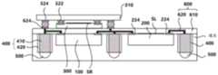
图2至图12是示出根据实施例的制造半导体封装件的方法的每个操作的示意性工艺的截面图。图2是示出执行对发光元件200和半导体芯片100进行模制的操作的结果的视图(S100)。参考图2,将电信号传输到形成在半导体芯片100中的电路并且将形成在电路中的电信号提供到外部的焊盘102可位于半导体芯片100的一个表面上。此外,电极224可位于发光元件200的一个表面上。2 to 12 are cross-sectional views illustrating schematic processes of each operation of the method of manufacturing a semiconductor package according to an embodiment. FIG. 2 is a view showing a result of performing an operation of molding the
图3(a)是示出发光元件200的发光面SL的视图,图3(b)是示出发光元件200的横截面的视图。根据实施例的发光元件200可以是诸如垂直腔面发射激光器(VCSEL)、发光二极管(LED)等的发光元件,并且可提供诸如红外光、可见光、紫外光等的波长范围内的光。3( a ) is a view showing the light emitting surface SL of the
请参照图3(a),发光元件200包括发光表面SL以及背面SB。多个光源222可位于发光表面SL上,并且提供驱动功率以使得发光元件200发射光的第一电极224位于发光表面SL上。第二电极226位于与发光表面SL相对的背面SB上。Referring to FIG. 3( a ), the
例如,第一电极224可连接到光源222的阳极电极,并且第二电极226可连接到光源222的阴极电极。作为另一示例,第一电极224可连接到光源222的阴极电极,并且第二电极226可连接到光源222的阳极电极。作为又一示例,由于第一电极被配置为两个电极并因此在发光表面SL上包括阳极电极和阴极电极两者,因此可在后表面SB上使用不具有电极的元件。For example, the
如图3(a)和图3(b)所示,由于发光元件200和第二电极226的厚度较薄,因此可能难以处理。此外,即使结合用于向第二电极226提供驱动功率的母衬底1000(参见图13),也可能存在由于第二电极226和发光元件200的厚度而发生限制的情况。As shown in FIG. 3( a ) and FIG. 3( b ), since the thickness of the
然而,在本实施例中,如图3(c)所示,在第二电极226上形成导电粘合层227,并且接合比第二电极226厚的金属图案220。因此,可克服由于发光元件200和第二电极226的厚度引起的限制。However, in the present embodiment, as shown in FIG. 3( c ), a conductive
在所示实施例中,导电粘合层227可包括银环氧树脂,并且导电金属图案220是诸如铜图案、铝图案、金图案等的导电金属图案,并且可由具有良好导电性的金属材料形成。此外,金属图案220的厚度d2可以是第二电极226的厚度d1的至少两倍,并且优选地是三倍或更多。In the illustrated embodiment, the conductive
在另一个实施例中(未示出),导电金属图案可包括形成有导电通路的非金属材料。作为另一实施例(未示出),导电粘合剂层227可由诸如金-锡(AuSn)等的材料形成,并且可使用共晶接合(eutectic bonding)来接合第二电极226和金属图案220。In another embodiment (not shown), the conductive metal pattern may include a non-metallic material formed with a conductive path. As another example (not shown), the conductive
作为又一实施例,可通过在第二电极226上形成由诸如铜、金、镍等的导电金属形成的纳米颗粒并烧结纳米颗粒来形成导电金属图案220。导电金属纳米颗粒可以分散在溶剂中,然后可以以喷涂、施加等形式形成至第二电极226。As yet another example, the
在图3(a)至图3(c)所示的实施例中,尽管示出了发光元件,但是导电金属图案120可以以类似的方式附接至半导体芯片100。附接至半导体芯片100的导电金属图案120和附接至发光元件200的导电金属图案220不仅可以向发光元件200和半导体芯片100提供驱动功率,而且还可以用作散热器。In the embodiment shown in FIGS. 3( a ) to 3 ( c ), although a light emitting element is shown, the
再次参考图2,在通路400的端部上形成外部连接端子500。通路400可包括由导电材料形成的导电杆410和封装导电杆的壳体420。Referring again to FIG. 2 ,
外部连接端子500可形成于导电杆410的端部处。例如,如图所示,外部连接端子500可以是焊球。可通过在形成用于在导电杆410的端部上电镀的籽晶层(未示出)之后实施回流,然后实施电镀以形成诸如锡、银等的焊料材料来形成焊球。在另一示例(未示出)中,外部连接端子可以是可连接到形成在母衬底上的焊球等的焊盘。在又一示例中,外部连接端子可以是导电凸块。An
形成有外部连接端子500的导电杆410和壳体420可在封装剂中模制在一起,并且外部连接端子500可通过稍后的工艺暴露以形成通路400(参见图8)。外部连接端子500可接合到位于母衬底1000上的连接端子(参见图13)以电连接封装件和母衬底1000(参见图13)。The
使用封装剂模制半导体芯片100和发光元件200(S100)。在模制工艺中,可模制多个半导体芯片和多个发光元件。半导体芯片可以是驱动光接收元件并负责信号处理或驱动存储器、算术元件和发光元件的芯片。可选地,半导体芯片可包括能够测量封装件中的温度的元件。此外,半导体模具可还包括光接收元件。在这种情况下,光接收元件可用作监测器,用于检测通过保持器(900,参见图12或图13)固定在其上的诸如透镜、漫射器等光学构件的损坏。作为另一示例,光接收元件可以是用于执行飞行时间(TOF)感测的辅助传感器。The
封装剂可以是环氧模制化合物(EMC),并且在封装剂(模具)固化之后与载体衬底(未示出)分离。如图所示,形成在通路400的端部上的外部连接端子500可以掩埋在固化的封装剂(模具)中,但是在稍后的工艺中暴露于外部(参见图8)。The encapsulant may be an epoxy molding compound (EMC) and is separated from the carrier substrate (not shown) after the encapsulant (mold) has cured. As shown, the
所示实施例示出了使用形成有外部连接端子500的导电杆410来形成通路400,但是根据实施例(未示出),通路可通过以下形成:将具有比模具低的硬度的牺牲构件(未示出)模制在一起,然后形成穿过牺牲构件的通孔,并且在通孔中形成导电材料。The illustrated embodiment shows that the via 400 is formed using the
例如,可通过诸如打孔、蚀刻等的方法来实施形成通孔的操作。形成导电材料的操作可通过在通孔中形成导电材料至少达到形成穿过模具的导电路径的程度来执行。For example, the operation of forming a via hole may be performed by a method such as drilling, etching, or the like. Forming the conductive material may be performed by forming the conductive material in the vias at least to the extent that a conductive path is formed through the die.
图4是示意性地示出形成电连接半导体芯片100和发光元件200的再分布层(RDL)600的操作的视图。再分布层600包括引线图案620,引线图案620电连接诸如绝缘层610和半导体芯片100的元件、发光元件200和光接收元件300(参见图5),这些元件在后续工艺中布置。FIG. 4 is a view schematically showing an operation of forming a redistribution layer (RDL) 600 electrically connecting the
绝缘层610可由诸如聚酰亚胺等的聚合物和氧化物膜中的一种形成,并且可钝化半导体芯片100和发光元件200以防止外部环境中的异物渗透到内部。The insulating
再分布层600可形成于发光元件200的发光表面SL上。引线图案620被布置为避开发光元件200的发光表面SL,使得由发光元件200提供的光不被再分布层600阻挡、散射、衍射或折射。此外,绝缘层610包括能够透射由发光元件100发射的波段中的光的材料。例如,绝缘层610可由诸如聚酰亚胺等的聚合物和氧化物膜中的一种形成,其在发光元件100提供940nm波段的光时具有90%或更大的透射率。引线图案620可由诸如铜、铝、金等具有高导电性的材料形成。The
可在再分布层600上形成焊盘624,焊盘624可在后续工艺中电连接到位于其上的元件。焊盘624可通过开口以形成在期望位置处连接到引线图案的焊盘并执行电镀来形成。由于焊盘624可由例如铜形成并且在空气中会容易氧化,所以可实施涂覆以提高与焊盘624的接合强度。
例如,焊盘624可涂覆有化学镀镍化学镀钯浸金(ENEPIG),其中,化学镀镍、化学镀钯和金层堆叠在铜图案上。作为另一示例,焊盘624可涂覆有化学镀镍浸金(ENIG),其中,化学镀镍和金层堆叠在铜图案上。作为又一示例,在焊盘624中,可使用热空气调平(HAL)将锡(Sn)涂覆在铜焊盘上。作为又一实例,铜焊盘624可涂覆有通过有机可焊性保护剂(OSP)选择性地接合至铜的有机材料。For example, the
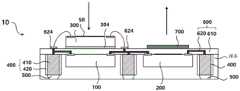
光接收元件300布置在再分布层600上以电连接到再分布层600(S400)。图5是示出光接收元件300布置在再分布层上以电连接到再分布层的状态的截面图。图6是示出根据另一实施例的光接收元件300布置在再分布层上以电连接至再分布层的状态的轮廓的视图。The
图5所示的实施例示出了焊盘624和光接收元件300通过引线接合而电连接。再分布层600和光接收元件300可通过位于光接收元件300的接合表面上的粘合剂层304机械地连接。当光接收元件300连接至再分布层600时,发光元件200的发光表面SL和光接收元件300的光接收表面SR可以面向相同的方向。The embodiment shown in FIG. 5 shows that the
根据本实施例(未示出),焊盘624与光接收元件300之间的电连接可通过耦接形成于光接收元件的背面上的外部连接端子(例如,导电凸块、焊球等)与焊盘624来进行。According to this embodiment (not shown), the electrical connection between the
图6所示的实施例示出了焊盘624通过电连接到光接收元件300的光传输衬底310电连接到光接收元件300。在一个实施例中,衬底310可为由例如玻璃、聚碳酸酯(PC)等材料形成的透明衬底。衬底310可以不是完全透明的,并且只有光穿过的部分可以是部分透明的,或者可以提供腔以使光穿过。The embodiment shown in FIG. 6 shows that the
在图6所示的实施例中,光接收元件300被布置为通过衬底310接收光。衬底310具有焊盘322和用于与光接收元件300电连接的连接构件,并且电连接到光接收元件300。衬底310可包含电连接到形成于重布层600上的焊盘624的焊盘。In the embodiment shown in FIG. 6 , the
在图6所示的实施例中,描述了形成在透明衬底310上的焊盘322与光接收元件之间的电连接、形成在透明衬底310上的焊盘324以及形成在再分布层600上的焊盘624全部通过焊球形成的示例,但是焊盘可由导电凸块和焊盘中的一个形成。In the embodiment shown in FIG. 6, the electrical connection between the
图7(a)至图7(c)是从顶部观察的封装件的平面图。参照图5至图7(c),光接收元件300位于半导体芯片100上方,并且光接收元件300的至少一部分被布置为位于半导体芯片100上。如图7(a)所示,光接收元件300可以位于半导体芯片100的正上方。在图7(b)和图7(c)所示的实施例中,半导体芯片100和光接收元件300可具有不同的横截面面积。光接收元件300可位于半导体芯片100上方,并且光接收元件300的至少一部分可位于半导体芯片100的正上方。此外,如图7(c)所示,半导体芯片100正上方的部分可包括在光接收元件300的横截面区域内。可通过以这种方式布置光接收元件300来减小制造的封装件的面积。7(a) to 7(c) are plan views of the package viewed from the top. Referring to FIGS. 5 to 7( c ), the
图5至图7示出了光接收元件300布置在再分布层600上的实施例。然而,如图14所示,光接收元件300可通过母衬底1000连接到封装(参见图14)。在半导体芯片100与导电金属图案120一起模制并且发光元件200与导电金属图案220一起模制之后,导电金属图案120和导电金属图案220可通过研磨工艺与外部连接端子500一起暴露(参见图8)。5 to 7 illustrate an embodiment in which the
图8是示出露出外部连接端子500的状态的视图。在一个实施例中,通过研磨封装件10的背面来暴露外部连接端子500。例如,可通过诸如研磨、化学机械研磨(CMP)、机械研磨等的工艺实施研磨工艺。当暴露外部连接端子500时,可通过根据实施例的封装件和母衬底(未示出)的连接来执行电连接。FIG. 8 is a view showing a state where the
描述了在光接收元件300布置在再分布层600上之后执行图8中所示的工艺的示例。然而,研磨工艺不仅可在光接收元件300布置在再分布层600上之后执行,而且可在光接收元件300布置在再分布层600上之前执行。An example in which the process shown in FIG. 8 is performed after the
虽然在附图中未示出,但是在封装件中,可在绝缘层610上进一步形成包括电阻器、电感器和电容器中的至少一个的无源元件。无源元件可形成在再分布层600上。图9是去除绝缘层610的至少一部分的状态的视图,绝缘层610位于由发光元件200提供的光的光路上。图9示出了导电金属图案120附接至半导体芯片100的背面并且导电金属图案220附接至发光元件200的背面的示例,并且示出了外部连接端子500、附接至半导体芯片100的背面的导电金属图案120和附接至发光元件200的背面的导电金属图案220在研磨工艺期间暴露的示例。Although not shown in the drawings, in the package, passive elements including at least one of resistors, inductors, and capacitors may be further formed on the insulating
当露出外部连接端子500、附接至半导体芯片100的导电金属图案120和附接至发光元件200的导电金属图案220时,可连接根据实施例的封装和母衬底(未示出)以形成电连接。例如,母衬底(未示出)可通过导电金属图案220向发光元件200提供参考电压VSS。此外,母衬底可通过导电金属图案120和外部连接端子500向半导体芯片100提供驱动功率。When the
在一个实施例中,去除由发光元件200提供的光通过的路径中的绝缘层610。去除绝缘层610的工艺可通过各向异性蚀刻来执行,并且可使用等离子体来执行。In one embodiment, the insulating
描述了在将光接收元件300布置在再分布层600上之后执行图9中所示的去除绝缘层610的一部分的操作的示例,但是这仅是示例,并且可通过在形成再分布层300的引线图案620的工艺中图案化绝缘层610来执行去除绝缘层610的一部分的操作。An example in which the operation of removing a part of the insulating
尽管图9示出了去除绝缘层610的一部分的示例,但是根据实施例(未示出),在发光表面SL上形成保护膜(未示出)之后,可通过完全去除绝缘层610直到暴露保护膜来实施使用等离子体的各向异性蚀刻工艺。然而,当绝缘层610由对由发光元件200提供的光具有90%或更高的高透射率的材料形成时,可不执行去除绝缘层610的工艺。Although FIG. 9 shows an example of removing a part of the insulating
图10是示意性地示出在由发光元件200提供的光的光路上形成透镜结构的状态的视图。参考图10,透镜结构804包括分别对应于光源222的位置的微透镜804(参见图3)。FIG. 10 is a view schematically showing a state where a lens structure is formed on an optical path of light supplied from the
根据另一实施例(未示出),透镜结构804可包括对由多个光源222提供的光执行光学处理的一个或多个透镜(参见图3)。例如,透镜结构800可包括聚集由一些光源222提供的光的第一透镜(参见图3)和准直由其余光源222提供的光的第二透镜(参见图3)。According to another embodiment (not shown), the
尽管描述了在去除绝缘层610之后实施形成透镜结构800的操作的示例,但是这仅是示例,并且可在形成再分布层600之后实施形成透镜结构800的操作。在另一实施例中,透镜结构800可布置在例如玻璃、聚碳酸酯(PC)等透明衬底上。微透镜804可通过光刻胶回流(PR回流)方法、喷墨方法、转印方法等形成。Although an example in which the operation of forming the lens structure 800 is performed after removing the insulating
图11是示意性地示出在发光元件200的发光表面上形成漫射构件700的状态的视图。参照图11,可通过在绝缘层610上施加光刻胶(PR),执行图案化以形成随机图案,然后回流随机图案来形成漫射构件700。在未示出的实施例中,漫射构件700可通过在诸如玻璃、聚碳酸酯(PC)等的透明衬底上形成漫射图案以漫射光来形成。漫射图案包括不规则形成的凹凸图案和不规则形成的直线图案(straight pattern.)。FIG. 11 is a view schematically showing a state in which the
在图11中,描述了在绝缘层610上形成漫射构件700的示例,但是这仅是示例,并且可在去除绝缘层610之后执行形成漫射构件700,并且可在形成再分布层600时在形成引线图案620之后形成漫射构件700。In FIG. 11 , an example of forming the
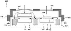
图12和图13是示出封装件10的构件保持器900的视图。在图12所示的实施例中,构件保持器900支撑位于发光元件200的光路上的光学构件920和位于光接收元件300的光路上的光学构件930。构件保持件900包括腿940,腿940包括引脚942。引脚942插入到形成在母衬底1000中的孔(未示出)中(参见图14)以将构件保持器900固定到母衬底(未示出)。12 and 13 are views showing the
光学构件920和930中的每一个可由单个透镜或多个透镜、漫射器、偏振滤光器、期望波段(红外(IR)、紫外(UV)、可见光等)的带通滤光器及其组合组成。例如,光学构件920和930可固定到光学构件壳体(未示出)并且耦接至光学构件保持器,并且光学构件壳体可以是例如固定透镜部分的镜筒。Each of
在图13所示的实施例中,构件保持器900支撑位于发光元件200的光路上的光学构件920和位于光接收元件300的光路上的光学构件930。构件保持件900的支腿940由再分布层600和封装件的侧壁SW支撑,并且粘合剂944布置在支腿940的面向再分布层600和封装件的侧壁SW的部分上。粘合剂944粘附至封装件的侧壁SW和再分布层600的上表面,并且将保持件900固定至封装件。In the embodiment shown in FIG. 13 , the
在图12和图13所示的实施例中,光学构件930和光学构件920分别布置在光接收元件300和发光元件200的光路上。因此,可通过处理提供给光接收元件300的光和由发光元件200提供的光来改善封装的光学性能。In the embodiments shown in FIGS. 12 and 13 , the
在图12和图13所示的实施例中,光学构件930被示出为凸透镜。然而,这仅是示例,并且通过包括凸透镜、凹透镜及其组合中的至少一个来执行使光会聚、发散和准直的一个或多个功能的光学构件可布置在构件保持器900中。此外,透镜可形成在发光元件200的光路上,并且在这种情况下,在构件保持器900中,漫射构件可布置在由发光元件200提供的光的光路上。In the embodiment shown in Figures 12 and 13, the
在下文中,将参照图8至图12描述根据实施例的封装件10。然而,为了简洁和清楚的描述,可省略对与上述元件相同或类似的元件的描述。图8至图14是示出根据实施例的光学元件半导体封装件10的轮廓的截面图。根据本实施例的光学元件半导体封装件10包括:发光元件200;光接收元件300;半导体芯片100,其中形成有半导体电路;模具,包覆半导体芯片100和发光元件200;再分布层600,电连接发光元件200、光接收元件300和半导体芯片300;通路400,电连接到再分布层600并穿过模具;以及外部连接端子500,电连接到通路,并且光接收元件300位于再分布层600上。Hereinafter, the
发光元件200可以是VCSEL和LED中的一个,并且可以提供波长范围内的光,诸如红外光、可见光、紫外光等。此外,发光元件200可输出期望波长范围内的激光。在一个实施例中,光接收元件300可以是检测期望波长范围内的光的光学元件,并且可以是光电二极管(PD)、互补金属氧化物半导体(CMOS)图像传感器(CIS)和单光子雪崩二极管(SPAD)中的一个。如图7(a)至图7(c)所示,光接收元件300的至少一部分可以位于半导体芯片100的正上方,因此提供了可减小半导体封装件的总面积的优点。The
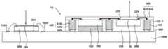
图14是示出封装件10的另一实施例的视图。参考图14,封装件10通过暴露的外部连接端子500以及导电金属图案120和220电连接到母衬底1000。驱动电路(未示出)、控制电路(未示出)、电源电路(未示出)等可位于母衬底1000中。封装件10可发送和接收电信号,并且从驱动电路(未示出)、控制电路(未示出)和电源电路(未示出)接收电力。FIG. 14 is a view showing another embodiment of the
光接收元件300可位于母衬底1000上,并且可通过形成在母衬底1000中的导电路径(未示出)电连接到封装件10、驱动电路(未示出)、控制电路(未示出)和电源电路(未示出)。The
在一个实施例中,封装件10和光接收元件300可通过各向异性导电膜(ACF)电连接到母衬底或通过表面安装技术(SMT)电连接到母衬底。In one embodiment, the
图15是示出根据实施例的封装件10的一个实施例的视图。参见图15,封装件10可被用于测量到目标T的距离。发光元件200从半导体芯片100接收驱动信号和/或功率并提供光。FIG. 15 is a view showing one embodiment of the
由发光元件200提供的光沿光路行进。在一个实施例中,封装件10包括构件保持器900,并且构件保持器900包括布置在发光元件200的光路和光接收元件300的光路上的光学构件,以执行使光会聚、发散和准直的一个或多个功能。Light provided by the
光从目标T反射并通过光路L提供给光接收元件230。半导体芯片100驱动发光元件200,使得发光元件200发射光,并且接收与由光接收元件300检测到的反射光相对应的电信号。半导体芯片100可计算从发光元件200发射光的时间到光接收元件300检测到光的时间的时间差(TOF:飞行时间),并且计算对应于时间差的距离。所计算的距离对应于光学元件半导体封装件10与目标T之间的距离。计算的时间差或距离可通过外部连接端子500提供给外部装置(未示出)。The light is reflected from the target T and supplied to the light receiving element 230 through the optical path L. As shown in FIG. The
尽管附图中所示的实施例被描述为用于帮助理解本发明的参考,但是它们是用于实现的实施例,并且仅仅是示例性的,本领域技术人员可执行各种修改和等同物。因此,本发明的真实技术范围应由所附权利要求限定。Although the embodiments shown in the drawings are described as references to help understanding of the present invention, they are embodiments for implementation and are merely exemplary, and various modifications and equivalents can be performed by those skilled in the art . Therefore, the true technical scope of the present invention should be defined by the appended claims.
Claims (35)
Translated fromChineseApplications Claiming Priority (3)
| Application Number | Priority Date | Filing Date | Title |
|---|---|---|---|
| KR20200072530 | 2020-06-15 | ||
| KR10-2020-0072530 | 2020-06-15 | ||
| PCT/KR2021/007437WO2021256815A1 (en) | 2020-06-15 | 2021-06-15 | Semiconductor package and method for manufacturing semiconductor package |
Publications (1)
| Publication Number | Publication Date |
|---|---|
| CN115867828Atrue CN115867828A (en) | 2023-03-28 |
Family
ID=79164360
Family Applications (1)
| Application Number | Title | Priority Date | Filing Date |
|---|---|---|---|
| CN202180050150.1APendingCN115867828A (en) | 2020-06-15 | 2021-06-15 | Semiconductor package and method of manufacturing the same |
Country Status (4)
| Country | Link |
|---|---|
| US (1) | US20230268331A1 (en) |
| KR (1) | KR102715554B1 (en) |
| CN (1) | CN115867828A (en) |
| WO (1) | WO2021256815A1 (en) |
Families Citing this family (3)
| Publication number | Priority date | Publication date | Assignee | Title |
|---|---|---|---|---|
| EP4481816A1 (en)* | 2022-02-14 | 2024-12-25 | Lipac Co., Ltd. | Optical system-in-package, and optical module and optical transceiver using same |
| US12040321B2 (en)* | 2022-09-20 | 2024-07-16 | Advanced Semiconductor Engineering, Inc. | Optical device including an optical component an electrical component, assembly structure including an optical component an electrical component and method for manufacturing the same |
| US20240241231A1 (en)* | 2023-01-13 | 2024-07-18 | Meta Platforms Technologies, Llc | Stacked time-of-flight module |
Citations (5)
| Publication number | Priority date | Publication date | Assignee | Title |
|---|---|---|---|---|
| US20150262983A1 (en)* | 2014-03-14 | 2015-09-17 | Avago Technologies General Ip (Singapore) Pte. Ltd. | METHODS FOR PERFORMING EXTENDED WAFER-LEVEL PACKAGING (eWLP) AND eWLP DEVICES MADE BY THE METHODS |
| CN106233460A (en)* | 2014-03-10 | 2016-12-14 | 德卡技术股份有限公司 | Semiconductor device and manufacture method thereof including the redistributing layer thickeied |
| US20180082990A1 (en)* | 2016-09-20 | 2018-03-22 | Kabushiki Kaisha Toshiba | Optical semiconductor module and method of manufacturing the same |
| KR20190044487A (en)* | 2017-10-20 | 2019-04-30 | 주식회사 네패스 | Optical module |
| CN110911427A (en)* | 2018-09-14 | 2020-03-24 | 三星电子株式会社 | Semiconductor package and method of manufacturing the same |
Family Cites Families (8)
| Publication number | Priority date | Publication date | Assignee | Title |
|---|---|---|---|---|
| JP4426279B2 (en)* | 2003-12-25 | 2010-03-03 | ローム株式会社 | Infrared data communication module |
| US8996818B2 (en)* | 2012-12-09 | 2015-03-31 | Advanced Micro Devices, Inc. | Bypassing memory requests to a main memory |
| CN106104296B (en)* | 2014-03-14 | 2020-01-21 | 赫普塔冈微光有限公司 | Optical imaging module and optical detection module including time-of-flight sensor |
| US10165954B2 (en)* | 2014-07-31 | 2019-01-01 | Salutron Inc. | Integrated sensor modules |
| KR102711354B1 (en)* | 2016-08-09 | 2024-09-26 | 엘지이노텍 주식회사 | Optical sensor module and Method for manufacturing optical sensor module |
| KR102206368B1 (en)* | 2017-12-05 | 2021-01-22 | 주식회사 라이팩 | Connector Plug and Active Optical Cable Assembly Using the Same |
| WO2020033001A2 (en)* | 2018-02-13 | 2020-02-13 | Sense Photonics, Inc. | Methods and systems for high-resolution long-range flash lidar |
| US11133423B2 (en)* | 2019-07-03 | 2021-09-28 | Advanced Semiconductor Engineering, Inc. | Optical device and method of manufacturing the same |
- 2021
- 2021-06-15CNCN202180050150.1Apatent/CN115867828A/enactivePending
- 2021-06-15USUS18/010,378patent/US20230268331A1/enactivePending
- 2021-06-15WOPCT/KR2021/007437patent/WO2021256815A1/ennot_activeCeased
- 2021-06-15KRKR1020210077633Apatent/KR102715554B1/enactiveActive
Patent Citations (5)
| Publication number | Priority date | Publication date | Assignee | Title |
|---|---|---|---|---|
| CN106233460A (en)* | 2014-03-10 | 2016-12-14 | 德卡技术股份有限公司 | Semiconductor device and manufacture method thereof including the redistributing layer thickeied |
| US20150262983A1 (en)* | 2014-03-14 | 2015-09-17 | Avago Technologies General Ip (Singapore) Pte. Ltd. | METHODS FOR PERFORMING EXTENDED WAFER-LEVEL PACKAGING (eWLP) AND eWLP DEVICES MADE BY THE METHODS |
| US20180082990A1 (en)* | 2016-09-20 | 2018-03-22 | Kabushiki Kaisha Toshiba | Optical semiconductor module and method of manufacturing the same |
| KR20190044487A (en)* | 2017-10-20 | 2019-04-30 | 주식회사 네패스 | Optical module |
| CN110911427A (en)* | 2018-09-14 | 2020-03-24 | 三星电子株式会社 | Semiconductor package and method of manufacturing the same |
Also Published As
| Publication number | Publication date |
|---|---|
| WO2021256815A1 (en) | 2021-12-23 |
| KR102715554B1 (en) | 2024-10-11 |
| KR20210155382A (en) | 2021-12-22 |
| US20230268331A1 (en) | 2023-08-24 |
Similar Documents
| Publication | Publication Date | Title |
|---|---|---|
| US9177884B2 (en) | Two-sided-access extended wafer-level ball grid array (eWLB) package, assembly and method | |
| US9786820B2 (en) | Opto-electronic module and method for manufacturing the same | |
| CN115867828A (en) | Semiconductor package and method of manufacturing the same | |
| US9525094B2 (en) | Proximity and ranging sensor | |
| US9583666B2 (en) | Wafer level packaging for proximity sensor | |
| US8017436B1 (en) | Thin substrate fabrication method and structure | |
| JP5461897B2 (en) | Optical waveguide laminated wiring board, manufacturing method thereof and mounting structure | |
| US11651976B2 (en) | Embedded packaging concepts for integration of ASICs and optical components | |
| JPH08327843A (en) | Optical waveguide module and its manufacture | |
| CN112447696B (en) | Display module package | |
| TW201436294A (en) | Optoelectronic device with laminated leadless carrier package oriented in lateral or topographical orientation (1) | |
| CN107808856A (en) | Semiconductor package structure and manufacturing method thereof | |
| JP6891101B2 (en) | Optical waveguide device, lens parts | |
| CN111384004B (en) | Semiconductor packaging device and manufacturing method thereof | |
| CN114341692A (en) | Bonded structure and method for making a bonded structure | |
| JP2017143126A (en) | Electronic apparatus and light-emitting/receiving device | |
| US11515261B2 (en) | Multiple component integration in fanout package with different back side metallization and thicknesses | |
| TWI797930B (en) | Optoelectronic package structure | |
| CN218350539U (en) | package | |
| US9459418B2 (en) | Flip chip optical communication apparatus | |
| JP3670220B2 (en) | Manufacturing method of semiconductor device | |
| TWI487151B (en) | Package of photoelectric device and photoelectric module | |
| CN116569323A (en) | Optical device package and method of manufacturing the same | |
| KR20220148481A (en) | Manufacturing method of light sensor package and light sensor package | |
| KR20210072722A (en) | Electronic devices and methods of manufacturing electronic devices |
Legal Events
| Date | Code | Title | Description |
|---|---|---|---|
| PB01 | Publication | ||
| PB01 | Publication | ||
| SE01 | Entry into force of request for substantive examination | ||
| SE01 | Entry into force of request for substantive examination |