CN115836378A - Treatment Kits with Protective Ceramic Coatings for Hydrogen and Ammonia Plasma Applications - Google Patents
Treatment Kits with Protective Ceramic Coatings for Hydrogen and Ammonia Plasma ApplicationsDownload PDFInfo
- Publication number
- CN115836378A CN115836378ACN202180049466.9ACN202180049466ACN115836378ACN 115836378 ACN115836378 ACN 115836378ACN 202180049466 ACN202180049466 ACN 202180049466ACN 115836378 ACN115836378 ACN 115836378A
- Authority
- CN
- China
- Prior art keywords
- disposed
- yttria
- chamber
- liner
- chamber body
- Prior art date
- Legal status (The legal status is an assumption and is not a legal conclusion. Google has not performed a legal analysis and makes no representation as to the accuracy of the status listed.)
- Pending
Links
Images


Classifications
- H—ELECTRICITY
- H01—ELECTRIC ELEMENTS
- H01J—ELECTRIC DISCHARGE TUBES OR DISCHARGE LAMPS
- H01J37/00—Discharge tubes with provision for introducing objects or material to be exposed to the discharge, e.g. for the purpose of examination or processing thereof
- H01J37/32—Gas-filled discharge tubes
- H01J37/32431—Constructional details of the reactor
- H01J37/32458—Vessel
- H01J37/32477—Vessel characterised by the means for protecting vessels or internal parts, e.g. coatings
- H01J37/32495—Means for protecting the vessel against plasma
- B—PERFORMING OPERATIONS; TRANSPORTING
- B08—CLEANING
- B08B—CLEANING IN GENERAL; PREVENTION OF FOULING IN GENERAL
- B08B7/00—Cleaning by methods not provided for in a single other subclass or a single group in this subclass
- B08B7/0035—Cleaning by methods not provided for in a single other subclass or a single group in this subclass by radiant energy, e.g. UV, laser, light beam or the like
- H—ELECTRICITY
- H01—ELECTRIC ELEMENTS
- H01J—ELECTRIC DISCHARGE TUBES OR DISCHARGE LAMPS
- H01J37/00—Discharge tubes with provision for introducing objects or material to be exposed to the discharge, e.g. for the purpose of examination or processing thereof
- H01J37/32—Gas-filled discharge tubes
- H01J37/32431—Constructional details of the reactor
- H01J37/3244—Gas supply means
- H—ELECTRICITY
- H01—ELECTRIC ELEMENTS
- H01J—ELECTRIC DISCHARGE TUBES OR DISCHARGE LAMPS
- H01J37/00—Discharge tubes with provision for introducing objects or material to be exposed to the discharge, e.g. for the purpose of examination or processing thereof
- H01J37/32—Gas-filled discharge tubes
- H01J37/32431—Constructional details of the reactor
- H01J37/32458—Vessel
- H01J37/32513—Sealing means, e.g. sealing between different parts of the vessel
- H—ELECTRICITY
- H01—ELECTRIC ELEMENTS
- H01L—SEMICONDUCTOR DEVICES NOT COVERED BY CLASS H10
- H01L21/00—Processes or apparatus adapted for the manufacture or treatment of semiconductor or solid state devices or of parts thereof
- H01L21/67—Apparatus specially adapted for handling semiconductor or electric solid state devices during manufacture or treatment thereof; Apparatus specially adapted for handling wafers during manufacture or treatment of semiconductor or electric solid state devices or components ; Apparatus not specifically provided for elsewhere
- H01L21/683—Apparatus specially adapted for handling semiconductor or electric solid state devices during manufacture or treatment thereof; Apparatus specially adapted for handling wafers during manufacture or treatment of semiconductor or electric solid state devices or components ; Apparatus not specifically provided for elsewhere for supporting or gripping
- H01L21/6831—Apparatus specially adapted for handling semiconductor or electric solid state devices during manufacture or treatment thereof; Apparatus specially adapted for handling wafers during manufacture or treatment of semiconductor or electric solid state devices or components ; Apparatus not specifically provided for elsewhere for supporting or gripping using electrostatic chucks
- H01L21/6833—Details of electrostatic chucks
- H—ELECTRICITY
- H01—ELECTRIC ELEMENTS
- H01J—ELECTRIC DISCHARGE TUBES OR DISCHARGE LAMPS
- H01J2237/00—Discharge tubes exposing object to beam, e.g. for analysis treatment, etching, imaging
- H01J2237/32—Processing objects by plasma generation
- H01J2237/33—Processing objects by plasma generation characterised by the type of processing
- H01J2237/334—Etching
- H—ELECTRICITY
- H01—ELECTRIC ELEMENTS
- H01J—ELECTRIC DISCHARGE TUBES OR DISCHARGE LAMPS
- H01J2237/00—Discharge tubes exposing object to beam, e.g. for analysis treatment, etching, imaging
- H01J2237/32—Processing objects by plasma generation
- H01J2237/33—Processing objects by plasma generation characterised by the type of processing
- H01J2237/335—Cleaning
- H—ELECTRICITY
- H01—ELECTRIC ELEMENTS
- H01L—SEMICONDUCTOR DEVICES NOT COVERED BY CLASS H10
- H01L21/00—Processes or apparatus adapted for the manufacture or treatment of semiconductor or solid state devices or of parts thereof
- H01L21/67—Apparatus specially adapted for handling semiconductor or electric solid state devices during manufacture or treatment thereof; Apparatus specially adapted for handling wafers during manufacture or treatment of semiconductor or electric solid state devices or components ; Apparatus not specifically provided for elsewhere
- H01L21/67005—Apparatus not specifically provided for elsewhere
- H01L21/67011—Apparatus for manufacture or treatment
- H01L21/67017—Apparatus for fluid treatment
- H01L21/67028—Apparatus for fluid treatment for cleaning followed by drying, rinsing, stripping, blasting or the like
- H—ELECTRICITY
- H01—ELECTRIC ELEMENTS
- H01L—SEMICONDUCTOR DEVICES NOT COVERED BY CLASS H10
- H01L21/00—Processes or apparatus adapted for the manufacture or treatment of semiconductor or solid state devices or of parts thereof
- H01L21/67—Apparatus specially adapted for handling semiconductor or electric solid state devices during manufacture or treatment thereof; Apparatus specially adapted for handling wafers during manufacture or treatment of semiconductor or electric solid state devices or components ; Apparatus not specifically provided for elsewhere
- H01L21/67005—Apparatus not specifically provided for elsewhere
- H01L21/67011—Apparatus for manufacture or treatment
- H01L21/67017—Apparatus for fluid treatment
- H01L21/67063—Apparatus for fluid treatment for etching
- H01L21/67069—Apparatus for fluid treatment for etching for drying etching
Landscapes
- Physics & Mathematics (AREA)
- Engineering & Computer Science (AREA)
- Plasma & Fusion (AREA)
- Chemical & Material Sciences (AREA)
- Analytical Chemistry (AREA)
- Optics & Photonics (AREA)
- Condensed Matter Physics & Semiconductors (AREA)
- General Physics & Mathematics (AREA)
- Manufacturing & Machinery (AREA)
- Computer Hardware Design (AREA)
- Microelectronics & Electronic Packaging (AREA)
- Power Engineering (AREA)
- Drying Of Semiconductors (AREA)
Abstract
Translated fromChinese
Description
Translated fromChinese技术领域technical field
本公开内容的实施方式一般涉及陶瓷涂布的部件、及包括其的基板处理腔室。Embodiments of the present disclosure generally relate to ceramic coated components, and substrate processing chambers including the same.
背景技术Background technique
在半导体工业中,器件的产生尺寸不断减小。一些制造工艺包括等离子体蚀刻及等离子体清洁工艺以将基板暴露于等离子体的高速流来蚀刻或清洁基板。氢等离子体工艺是特别有用的,但是高度腐蚀性的并且可腐蚀处理腔室内的部件。对腔室部件的腐蚀产生颗粒,所述颗粒污染所处理的基板并且导致器件缺陷。In the semiconductor industry, devices are produced in ever-decreasing dimensions. Some fabrication processes include plasma etching and plasma cleaning processes to etch or clean the substrate by exposing the substrate to a high velocity flow of plasma. Hydrogen plasma processes are particularly useful, but are highly corrosive and can corrode components within the processing chamber. Erosion of chamber components produces particles that contaminate processed substrates and cause device defects.
随着器件几何尺寸缩小,对缺陷的易感性增加,并且颗粒污染物要求变得更加严格。由此,随着器件几何尺寸缩小,颗粒污染的可允许水平可能降低。为了最小化由等离子体蚀刻和/或等离子体清洁工艺引入的颗粒污染,已经开发了对等离子体具有抗性的腔室材料。此种抗等离子体材料的实例包括由Al2O3、AlN、SiC、Y2O3、石英、及ZrO2构成的陶瓷。不同陶瓷提供不同的材料性质,如抗等离子体性、刚性、挠曲强度、热冲击阻抗等等。此外,不同陶瓷具有不同的材料成本。As device geometries shrink, susceptibility to defects increases and particle contamination requirements become more stringent. Thus, as device geometries shrink, the allowable level of particle contamination may decrease. In order to minimize particle contamination introduced by plasma etching and/or plasma cleaning processes, plasma resistant chamber materials have been developed. Examples of such plasma resistant materials include ceramics composed of Al2 O3 , AlN, SiC, Y2 O3 , quartz, and ZrO2 . Different ceramics offer different material properties such as plasma resistance, rigidity, flexural strength, thermal shock resistance, and more. Furthermore, different ceramics have different material costs.
不同陶瓷涂层或陶瓷替换部件的位置及特性大幅度影响颗粒在基板上的沉积。由此,需要利用陶瓷涂层及陶瓷部件的组合,此组合最小化基板上的颗粒沉积,同时维持腔室的结构完整性并且降低总体成本。The position and properties of different ceramic coatings or ceramic replacement parts greatly influence the deposition of particles on the substrate. Thus, there is a need to utilize a combination of ceramic coatings and ceramic components that minimizes particle deposition on the substrate while maintaining the structural integrity of the chamber and reducing overall cost.
发明内容Contents of the invention
本公开内容通常涉及一种用于基板处理的设备,包括腔室主体、在腔室主体内设置的下部衬垫、在下部衬垫顶上并且在腔室主体内设置的上部衬垫、穿过上部衬垫及腔室主体设置的衬垫门、在腔室主体顶上设置的腔室盖、及穿过腔室盖设置的气体喷嘴。下部衬垫、上部衬垫、及衬垫门中的每一者进一步包括上面设置的喷涂的氧化钇锆层并且气体喷嘴是块体陶瓷气体喷嘴。The present disclosure generally relates to an apparatus for substrate processing comprising a chamber body, a lower liner disposed within the chamber body, an upper liner atop the lower liner and disposed within the chamber body, through A gasket door provided on the upper gasket and the chamber body, a chamber cover provided on top of the chamber body, and a gas nozzle provided through the chamber cover. Each of the lower gasket, the upper gasket, and the gasket door further included a sprayed yttrium zirconium oxide layer disposed thereon and the gas nozzles were bulk ceramic gas nozzles.
一种用于基板处理的设备的另一实施方式包括腔室主体、在腔室主体内设置的下部衬垫、在下部衬垫顶上并且在腔室主体内设置的上部衬垫、穿过上部衬垫及腔室主体设置的衬垫门、在上部衬垫顶上设置的腔室盖、穿过腔室盖设置的气体喷嘴、及在下部衬垫与上部衬垫之间、在上部衬垫与腔室盖之间、及在下部衬垫与基板支撑基座之间设置的一个或多个镀镍或不锈钢垫圈。下部衬垫、上部衬垫、及衬垫门进一步包括上面设置的喷涂的氧化钇锆层,其中氧化钇锆进一步包含Y2O3-ZrO2固溶体。气体喷嘴是块体陶瓷气体喷嘴。Another embodiment of an apparatus for substrate processing includes a chamber body, a lower liner disposed within the chamber body, an upper liner disposed atop the lower liner and within the chamber body, an upper liner disposed through the upper Gasket door set on the liner and chamber body, chamber cover set on top of the upper liner, gas nozzles set through the chamber cover, and between the lower liner and the upper liner, on the upper liner One or more nickel-plated or stainless steel washers disposed between the chamber lid and between the lower liner and the substrate support base. The lower liner, the upper liner, and the liner door further include a spray-coated yttria-zirconium layer disposed thereon, wherein the yttria-zirconium oxide further comprises aY2O3-ZrO2 solid solution. The gas nozzles are bulk ceramic gas nozzles.
一种用于基板处理的设备的又一实施方式包括腔室主体、在腔室主体内设置的下部衬垫、在下部衬垫顶上并且在腔室主体内设置的上部衬垫、穿过上部衬垫及腔室主体设置的衬垫门、在上部衬垫顶上设置的腔室盖、穿过腔室盖设置的气体喷嘴、在腔室盖之上设置的感应线圈、及在感应线圈与腔室盖之间设置的屏蔽电极。下部衬垫、上部衬垫、及衬垫门中的每一者进一步包含上面设置的喷涂的氧化钇锆层。气体喷嘴是块体陶瓷气体喷嘴。喷涂的氧化钇锆层的厚度是约25微米至约300微米并且喷涂的氧化钇锆层是具有浓度为99%或更大的Y2O3及ZrO2的纯化的氧化钇锆涂层。Yet another embodiment of an apparatus for substrate processing includes a chamber body, a lower liner disposed within the chamber body, an upper liner disposed atop the lower liner and within the chamber body, an upper liner disposed through the upper The liner door provided on the liner and the chamber main body, the chamber cover provided on the top of the upper liner, the gas nozzle provided through the chamber cover, the induction coil arranged on the chamber cover, and the induction coil and A shield electrode is placed between the chamber lids. Each of the lower liner, the upper liner, and the liner door further included a layer of sprayed yttrium zirconium oxide disposed thereon. The gas nozzles are bulk ceramic gas nozzles. The thickness of the sprayed yttria zirconium oxide layer is about 25 microns to about300 microns and the sprayed yttria zirconium oxide layer is a purified yttria zirconium oxide coating with a concentration of 99%Y2O3 andZrO2 .
附图说明Description of drawings
为了能够详细理解本公开内容的上述特征所用方式,可参考实施方式进行对上文简要概述的本公开内容的更特定描述,一些实施方式在附图中示出。然而,将注意,附图仅示出示例性实施方式,并且由此不被认为限制其范围,由于本公开内容可允许其他等同有效的实施方式。So that the manner in which the above recited features of the disclosure can be understood in detail, a more particular description of the disclosure, briefly summarized above, may have reference to embodiments, some of which are illustrated in the accompanying drawings. It is to be noted, however, that the appended drawings illustrate exemplary embodiments only and are therefore not to be considered limiting of its scope, for the present disclosure may admit to other equally effective embodiments.
图1是根据一个实施方式的处理腔室组件的示意性横截面图。Figure 1 is a schematic cross-sectional view of a processing chamber assembly according to one embodiment.
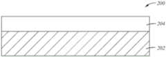
图2是陶瓷涂布的腔室部件的示意性横截面图。Figure 2 is a schematic cross-sectional view of a ceramic coated chamber component.
图3是处理基板的方法。Figure 3 is a method of processing a substrate.
图4是示出基板颗粒污染水平的图表。FIG. 4 is a graph showing the level of substrate particle contamination.
图5是示出由处理腔室盖导致的基板颗粒污染的曲线图。5 is a graph showing particle contamination of a substrate by a process chamber lid.
为了便于理解,相同附图标记在可能的情况下已经用于标识图中共有的相同元件。可预期,一个实施方式的元件及特征可有利地并入其他实施方式中,而无需进一步叙述。To facilitate understanding, identical reference numerals have been used, where possible, to identify identical elements that are common to the figures. It is contemplated that elements and features of one embodiment may be beneficially incorporated in other embodiments without further recitation.
具体实施方式Detailed ways
本文提供的公开内容的实施方式包括用于基板处理的处理腔室。处理腔室可在基板的氢等离子体处理期间利用。处理腔室包括多个腔室部件。多个腔室部件中的一个或多个利用如Y2O3-ZrO2固溶体的氧化钇锆组成物涂布。多个腔室部件中的一些腔室部件替换为块体氧化钇锆陶瓷。又一些腔室部件替换为不同材料的类似部件。执行涂布及部件替换,以便在涉及氢等离子体的基板处理操作期间减少基板的颗粒污染。Embodiments of the disclosure provided herein include processing chambers for substrate processing. The processing chamber may be utilized during hydrogen plasma processing of substrates. The processing chamber includes a plurality of chamber components. One or more of the plurality of chamber components is coated with a yttria-zirconium composition such as aY2O3 -ZrO2solid solution. Some of the plurality of chamber components were replaced with bulk yttrium zirconia ceramics. Still other chamber components were replaced with similar components of different materials. Coating and part replacement are performed to reduce particle contamination of substrates during substrate processing operations involving hydrogen plasma.
图1是根据一个实施方式的处理腔室组件100的示意性横截面图。如图所示,处理腔室组件100包括等离子体处理腔室101、等离子体源160、偏压功率(bias power)系统161、及控制器146。等离子体处理腔室101提供了用于处理已经在基板128的表面上形成的薄膜的腔室。通常,薄膜在单独的薄膜沉积腔室中的基板128的表面上沉积,该薄膜沉积腔室耦合到处理腔室组件100内共享的群集工具。在一些实施方式中,等离子体处理腔室101也可额外配置为在基板的表面上沉积薄膜层。等离子体源160将气态混合物134(如含氢气态混合物)转化为等离子体136,该等离子体轰击基板128以改变其上生长的膜的性质。偏压功率系统161提供整个基板128的电压偏压以促进处理工艺。控制器146实施用于膜生长及膜处理两者的具体处理条件。整个处理腔室组件100配置为使用具体等离子体工艺生长或处理在基板128上形成的膜,该等离子体工艺通过使用控制器146提供的命令来提供。薄膜处理工艺由等离子体源160及偏压功率系统161辅助。Figure 1 is a schematic cross-sectional view of a
如图所示,等离子体处理腔室101包括腔室主体106、腔室盖108、基板支撑基座104、静电夹盘105、电气接地116、气体面板130、具有入口132的气体喷嘴131、节流阀138、真空泵140及气源142。等离子体处理腔室101可以是任何适宜的等离子体处理腔室,如感应耦合等离子体(inductively coupled plasma;ICP)处理腔室。在一个实施方式中,处理腔室101及薄膜沉积腔室(未图示)是同一群集工具(未图示)的部分。群集工具(例如,来自应用材料公司(Applied Materials Inc.)的
如图1所示,处理腔室101包括腔室主体106、介电腔室盖108及在腔室主体106内设置的基板支撑基座104。腔室主体106及介电腔室盖108帮助隔离处理腔室101的内部空间与外部环境。通常,腔室主体106耦合到电气接地116。腔室主体106也可描述为处理腔室101的腔室壁。腔室主体106包括处理腔室101的侧壁及底壁。介电腔室盖108可由任何适宜的介电质(如石英)构成。针对一些实施方式,介电腔室盖108可采取不同形状(例如,圆顶形状)。在一些实施方式中,如本文进一步描述,腔室盖108可涂布有陶瓷涂层。具有入口132的气体喷嘴131流体连接到气体面板130及处理腔室101。气体喷嘴131是任何适宜的气体喷嘴并且包含块体陶瓷。块体陶瓷在下文进一步描述。As shown in FIG. 1 , the
开口154穿过腔室主体106形成。调节开口154的尺寸用于将基板传送进出处理腔室101。开口154在腔室主体106的侧壁上设置。开口154是在处理腔室组件100与群集工具(未图示)之间的阀的部分。开口154可以是狭缝阀或压紧及密封阀组件的部分。邻近开口154设置的阀的衬垫门156是锡或铅材料。衬垫门156包括陶瓷衬垫,如氧化钇锆。陶瓷衬垫可类似于本文描述的其他陶瓷衬垫。An
检测器122附接到腔室主体106以促进决定何时将腔室101内的气体混合物激励为等离子体。例如,检测器122可检测由激发的气体发射的辐射或使用光学发射光谱学(optical emission spectroscopy;OES)以测量与所产生的等离子体相关联的光的一个或多个波长的强度。整个等离子体源160利用气态混合物134产生等离子体136以处理所沉积的薄膜。A
腔室主体106包括上部腔室主体111及下部腔室主体113。上部腔室主体111是腔室主体106的上部部分,使得上部腔室主体111包括其中设置的开口154、检测器122、及节流阀138。上部腔室主体111邻近腔室盖108。上部腔室主体形成处理腔室101的至少一部分。上部腔室主体111进一步包括加衬于上部腔室主体111内侧的上部衬垫109。The
下部腔室主体113是腔室主体106的下部部分,使得下部腔室主体113包括其中设置的真空泵140及基座104。真空泵140在下部腔室主体113内的开口处设置。基座104在下部腔室主体113的一部分顶上设置。下部腔室主体113在上部腔室主体111下方设置。下部腔室主体113形成处理腔室101的至少一部分。下部腔室主体113进一步包括加衬于上部腔室主体111内侧的下部衬垫107。The
上部衬垫109及下部衬垫107分别在上部腔室主体111及下部腔室主体113的内表面上设置。上部衬垫109及下部衬垫107是具有锡、铅、或锡及铅涂层的铜。在一些实施方式中铜可以是铍铜。上部衬垫109及下部衬垫107进一步包括陶瓷涂层。陶瓷涂层是氧化钇锆涂层。氧化钇锆涂层在本文更详细描述。The
在操作中,基板128(如半导体基板)可放置在静电夹盘105上,并且处理气体可从气体面板130穿过入口132供应以致力于形成气态混合物134。根据一个实施方式,基板128是裸硅晶片。在另一实施方式中,如通常在逻辑门、I/O门、场效应晶体管、FINFET、或存储器应用中使用的,基板128是图案化的硅晶片。下文描述了可在本文描述的一个或多个工艺中使用的常见处理气体。气态混合物134可在处理腔室101中通过施加来自RF功率源(powersource)114的功率而激励为等离子体136。在处理腔室101的内部空间内的压力可使用节流阀138及真空泵140控制。在一些实施方式中,腔室主体106的温度可使用行进穿过腔室主体106的含液体导管(未图示)或者嵌入腔室主体106中(例如,加热筒或线圈)或缠绕在处理腔室101周围(例如,加热器包或带)的加热元件来控制。In operation, a
基板128的温度可通过控制基座104的温度来控制。通过使用加热及冷却元件,静电夹盘105的温度可控制为从20至500℃的范围。在处理期间将基板128“夹持”到静电夹盘105的基板支撑表面来主动地控制基板的温度。归因于离子轰击,经由嵌入基座104内的冷却元件对静电夹盘105及基板的温度控制帮助减小不期望的温度增加。将来自气源142的氦(He)气体经由气体导管144提供到在基板128下方的基座表面中形成的通道(未图标)。氦气可促进在基座104与基板128之间的热传递。在处理期间,可将基座104加热至稳态温度,并且随后氦气可促进基板128的均匀加热。基座104可由加热元件(未图标)如此加热,该加热元件诸如嵌入基座104内的电阻式加热器、或通常瞄准基座104或基板128(当在基座上时)的灯。使用此种热控制,基板128可维持在约20至500℃之间的第一温度下。等离子体源160的部件为膜生长及致密化提供环境。The temperature of the
等离子体屏蔽环129在基板128的外边缘周围并且在基座104顶上设置。等离子体屏蔽环129围绕基板128。等离子体屏蔽环129改进在基板128的边缘附近的处理(例如,沉积及蚀刻)的均匀性。等离子体屏蔽环129进一步保护基板128的下侧边缘。在如本文描述的实施方式中,等离子体屏蔽环129是块体陶瓷等离子体屏蔽环,使得等离子体屏蔽环129是氧化钇锆等离子体屏蔽环或氧化铝等离子体屏蔽环129。等离子体屏蔽环129也可以是具有氧化钇锆涂层的氧化铝环。氧化钇锆涂层可类似于本文描述的氧化钇锆涂层中的任一者。在一些实施方式中,等离子体屏蔽环129包含两个可附接/可分离的等离子体屏蔽环部件,使得两个可附接的等离子体屏蔽环部件接合彼此以形成多部件等离子体屏蔽环129。两个等离子体屏蔽环129的子部件中的每一者使用本文描述的陶瓷涂层中的任一者单独地涂布。A
基座104经由一个或多个紧固件164连接到腔室主体106的下部腔室主体113及下部衬垫107。一个或多个紧固件164穿过基座104的底部部分、下部腔室主体113、及下部衬垫107设置。一个或多个紧固件164可以是螺钉、螺栓、或任何其他适宜的紧固件。一个或多个紧固件164包括铅及锡。在一些实施方式中,一个或多个紧固件164可以是具有铅或锡涂层的铜紧固件。紧固件盖162在等离子体处理腔室101内设置的紧固件164的部分上方设置。紧固件盖162是块体陶瓷部分,如氧化钇锆陶瓷部分。或者,紧固件盖162可以是氧化铝陶瓷部分。在本文中进一步描述块体陶瓷紧固件盖162的组成物。一个或多个紧固件164及在紧固件164上设置的紧固件盖162绕着基座104的基底的外径设置。一个或多个紧固件164连接基座104、下部腔室主体113、及下部衬垫107并且将所述部件固定在一起。Base 104 is connected to
如图所示,等离子体源160包括线圈元件110、第一阻抗匹配网络112、RF功率源114、电气接地117、屏蔽电极118、电气接地119、开关120、及检测器122。在介电腔室盖108之上,包括至少一个感应线圈元件110的射频(RF)天线在其上设置。在一种配置中,如图1所示,绕着处理腔室的中心轴设置的两个同轴线圈元件在RF频率下驱动以在处理腔室组件100的处理区域中产生等离子体136。在一些实施方式中,感应线圈元件110可在腔室主体106的至少一部分周围设置。感应线圈元件110的一端可穿过第一阻抗匹配网络112耦合到RF功率源114,并且另一端可如图所示连接到电气接地117。功率源114在13.56MHz的频率下通常能够产生多达4千瓦(kW)。供应到感应线圈元件110的RF功率可在从1至100kHz变化的频率下脉冲(即,在开启及关闭状态之间切换)或功率循环(即,将功率输入从高电平改变到低电平)。等离子体136的平均离子密度可从1E10至1E12离子每立方厘米(cm-3)改变。等离子体密度可通过使用任何常规的等离子体诊断技术来测量,诸如通过使用自激发电子等离子体共振波谱学(Self Excited Electron Plasma Resonance Spectroscopy;SEERS)、朗缪尔(Langmuir)探头或其他适宜的技术。据信,在图1中示出的感应耦合的同轴线圈元件110配置在控制及产生高密度等离子体方面与包括电容耦合及等离子体源配置的常规等离子体源配置相比提供了显著优点。As shown,
屏蔽电极118插入RF天线的感应线圈元件110与介电腔室盖108之间。屏蔽电极118可替代地经由任何适宜手段电气浮动或耦合到电气接地119,该手段用于构成及断开电气连接,诸如如图1中示出的开关120。A
如图所示,偏压功率系统161包括第二阻抗匹配网络124、及偏压功率源126。基座104经由第二阻抗匹配网络124耦合到偏压功率源126。类似于RF功率源114,偏压功率源126通常能够产生具有在从1至160MHz的范围内的驱动频率及在约0kW与约3kW之间的功率的RF信号。利用13.56MHz的频率或2MHz的频率,偏压功率源126能够在从2至160MHz的范围中的频率下产生在约1W与1千瓦(kW)之间的功率。视情况,偏压功率源126可以是直流(DC)或脉冲DC源。在一些实施方式中,耦合到偏压功率源126的电极在静电夹盘105内设置。偏压功率系统161在整个基板128上提供基板电压偏压以促进对所沉积的薄膜的处理。在一个实施方式中,RF偏压提供具有多达2000eV的离子能量的高能离子。As shown in the figure, the
如图所示,控制器146包括中央处理单元(central processing unit;CPU)148、存储器150、及支持电路152。控制器146可与RF功率源114、开关120、检测器122、及偏压功率源126对接。控制器146可以是任何适宜类型的通用计算机处理器,该通用计算机处理器可在用于控制各个腔室及子处理器的工业环境中使用。存储器150、或用于CPU 148的其他计算机可读介质可以是任何容易获得的存储器形式中的一个或多个,如随机存取存储器(random access memory;RAM)、只读存储器(read only memory;ROM)、软盘、硬盘、或任何其他形式的数字储存器(本端或远程)。支持电路152可耦合到CPU 148,以致力于以常规方式支持处理器。这些电路可包括高速缓存、电源、时钟电路、输入/输出(I/O)电路及子系统、及类似者。针对一些实施方式,本文公开的用于激励及维持等离子体的技术可存储在存储器150中作为软件例程。软件例程也可由第二CPU(未图示)存储和/或执行,该第二CPU位于由CPU 148控制的硬件的远程。控制器146为处理腔室组件100及上文提及的各种子部件提供用于温度控制、偏压电压、气体流动速率、及类似者的指令。As shown, the
一个或多个垫圈166在腔室盖108与腔室主体106之间设置,使得一个或多个垫圈166在腔室盖108与上部腔室主体111之间设置。一个或多个垫圈166辅助维持在腔室盖108与腔室主体106之间的密封,同时也改进在腔室盖108与腔室主体106之间的电导率。垫圈166是镀镍铜垫圈或不锈钢垫圈。垫圈166是镀镍的,以便减少在基板处理期间由垫圈166导致的颗粒污染。使用不锈钢垫圈类似地减少处理腔室内的颗粒污染。已经发现,利用低熔点温度的金属作为垫圈166(如铅、锡、或铟涂布的垫圈)在基板上产生球或盘状缺陷。低熔点温度的金属(如铅及锡)在处理期间由氢等离子体提取。已经发现镍镀垫圈166显著减少由垫圈166导致的基板的颗粒污染。在垫圈166上的镀镍具有在约1微米至约3mm的范围内的厚度,如约25微米至约100微米,如约50微米至约80微米。类似地,已经显示用不锈钢垫圈替换低熔点温度的金属垫圈减少由常规垫圈导致的颗粒污染。One or
一个或多个垫圈168在上部腔室主体111与下部腔室主体113之间设置。一个或多个垫圈166辅助维持在上部腔室主体111与下部腔室主体113之间的密封,同时也提供在上部腔室主体111与下部腔室主体113之间的导电路径。垫圈166是镀镍铜垫圈或不锈钢垫圈。One or
一个或多个垫圈170在下部腔室主体113与基座104之间设置。一个或多个垫圈170辅助维持在下部腔室主体113与基座104之间的密封。垫圈170额外改进在下部腔室主体113与基座104之间的电气连接。垫圈170是镀镍铜垫圈或不锈钢垫圈。在一些实施方式中,垫圈170可在下部衬垫107与基座104之间设置。One or
图2是陶瓷涂布的腔室部件200的一部分的示意性横截面图。陶瓷涂布的腔室部件200可以是腔室盖108、上部衬垫109、下部衬垫107、衬垫门156、基座104、及静电夹盘105中的任一者。陶瓷涂布的腔室部件200包括部件202及陶瓷涂层204。部件202是腔室盖108、上部衬垫109、下部衬垫107、衬垫门156、基座104、或静电夹盘105中的任一者。FIG. 2 is a schematic cross-sectional view of a portion of a ceramic-coated
部件202可包括多个层,如用铅或锡层涂布的基底铜层。铜层可以是腔室部件200中的每一者的主要部件。基底铅或锡层可以是在主要部件与陶瓷涂层204之间的层。
在一些实施方式中,部件202是单一材料并且不包括多个层。单一材料可包含氧化铝、石英、或铜中的任一者。部件202具有直接在其上设置的陶瓷涂层204。In some embodiments,
陶瓷涂层204是在部件202顶上沉积的涂层以最小化在处理腔室组件100内的基板(如基板128)上沉积的污染颗粒。陶瓷涂层204可包含Y2O3-ZrO2固溶体。Y2O3-ZrO2固溶体是Y2O3及ZrO2化合物的固相溶体。Y2O3及ZrO2化合物呈单一均质相。Y2O3-ZrO2固溶体是约20分子百分比至约50分子百分比的ZrO2。在一些实施方式中,Y2O3-ZrO2固溶体是约25分子百分比至约45分子百分比的ZrO2,如约30分子百分比至约40分子百分比的ZrO2。在一些实施方式中,存在少量的Y2O液体残留物连同Y2O3-ZrO2单相。
陶瓷涂层204可具有约2%至约10%(例如,在一个实施方式中小于近似5%)的孔隙度的涂层。在一些实施方式中,陶瓷涂层204的孔隙度小于约3%,如小于2%,如小于1%。陶瓷涂层204具有近似3-8千兆帕(GPa)(例如,在一个实施方式中大于近似4GPa)的硬度,及近似8-20兆帕(MPa)(例如,在一个实施方式中大于近似10MPa)的热冲击阻抗。此外,陶瓷涂层可具有近似4-20MPa的粘附强度(例如,在一个实施方式中大于近似14MPa)。粘附强度可通过将力(例如,以兆帕测量)施加到陶瓷涂层直到陶瓷涂层从陶瓷基板剥离来决定。
陶瓷涂层204通过在陶瓷基板上喷涂或生长陶瓷涂层来形成。部件202通过烧结工艺或机械加工来形成。在喷涂陶瓷涂层204的实施方式中,陶瓷涂层204是喷涂的氧化钇锆。喷涂的氧化钇锆包括约10微米至约500微米的厚度,如约15微米至约400微米,如约20微米至约300微米,如约20微米至约250微米。喷涂有氧化钇锆的涂层部件使得陶瓷涂层204的厚度能够大于使用其他陶瓷沉积工艺沉积的物理气相沉积(physical vapor deposition;PVD)氧化钇锆涂层,并且防止陶瓷涂层204在大于约15微米的厚度下断裂。增加的厚度防止金属污染物在处理期间经过陶瓷涂层204并且降低维护频率。喷涂的氧化钇锆容易施加到大的部件202,如上部衬垫109、下部衬垫107、衬垫门156、及基座104。喷涂的氧化钇锆使用热喷涂技术和/或等离子体喷涂技术施加。热喷涂技术及等离子体喷涂技术可熔化材料(例如,陶瓷粉末)并且将熔化的材料喷涂到部件202上。陶瓷涂层可具有与块体陶瓷材料(例如,如陶瓷基板)的结构性质明显不同的结构性质。The
或者,陶瓷涂层204通过经由PVD涂布工艺在陶瓷基板上沉积陶瓷涂层来形成。在其中陶瓷涂层204使用PVD涂布工艺沉积的实施方式中,陶瓷涂层204是PVD涂布的氧化钇锆。PVD涂布的氧化钇锆包括小于约15微米的厚度,如小于约10微米,如约0.5微米至约10微米,如约0.75微米至约7.5微米,如约1微米至约5微米。将PVD涂布的氧化钇锆施加到较小的部件202,如腔室盖108。PVD涂布的氧化钇锆具有与喷涂的氧化钇锆相比较低的孔隙度。喷涂的氧化锆具有约0.5%至约5%的孔隙度,如约1%至约4%,如约2%至约3%。PVD涂布的氧化钇锆具有约0%至约1%的孔隙度,如约0%至约0.5%,如约0%至约0.25%。Alternatively,
PVD涂布的氧化钇锆是相对薄的涂层。因为PVD涂层能够承受邻近腔室盖108的氢等离子体的影响,因此PVD涂层有利地用于腔室盖108上。PVD涂层更容易在平坦表面(如腔室盖108的底表面)上沉积。第二氧化钇锆涂层的PVD涂布与喷涂的氧化钇锆的涂层上的喷涂相比是更均匀的并且具有较高的密度。PVD涂布工艺可替代地为CVD或ALD涂布工艺。CVD及ALD工艺可产生与PVD涂布类似的结果,如类似孔隙度及厚度。PVD coated yttrium zirconium oxide is a relatively thin coating. A PVD coating is advantageously used on the
在一些实施方式中,层压或烧结的氧化钇锆层形成在基板上,如在气体喷嘴131、等离子体屏蔽环129、腔室盖108、及/或紧固件盖162上。层压或烧结的氧化钇锆层可使用两种不同的沉积技术形成并且可具有改变的物理性质。在一些实施方式中,层压或烧结的氧化钇锆层通过在喷涂的氧化钇锆层顶上沉积PVD涂布的氧化钇锆层来形成。在喷涂的层顶上沉积PVD涂布的层形成层压的氧化钇锆层。层压的氧化钇锆层是由经由喷涂及PVD涂布连续一次或多次沉积氧化钇锆形成的层。In some embodiments, a laminated or sintered layer of yttrium zirconium oxide is formed on a substrate, such as on
在基板上形成第二氧化钇锆层之前,喷涂的氧化钇锆层在基板上形成。喷涂的氧化钇锆层类似于本文描述的喷涂的氧化钇锆层。喷涂的氧化钇锆层是低应力层,使得喷涂的氧化钇锆以低应力良好粘附到基板。PVD涂层(如PVD涂布的氧化钇锆)在喷涂的氧化钇锆层顶上沉积。当在基板本身上沉积时,PVD涂布的氧化钇锆层是与喷涂的氧化钇锆层相比较高应力的层。通过在喷涂的氧化钇锆层顶上沉积PVD涂布的氧化钇锆层,在PVD涂布的氧化钇锆层内的应力减小,使得在喷涂的氧化钇锆层顶上的PVD涂布的氧化钇锆层内的应力小于喷涂的氧化钇锆层的较高应力层,此是由于喷涂的氧化钇锆层用作桥接层。取决于喷涂及PVD涂布的氧化钇锆层的结构、孔隙度、及厚度,与PVD涂层本身相比在该涂层内的应力减小约10%至约90%。A sprayed yttria-zirconium oxide layer is formed on the substrate prior to forming the second yttrium-zirconium oxide layer on the substrate. The sprayed yttria zirconium oxide layer is similar to the sprayed yttrium zirconium oxide layer described herein. The sprayed yttria zirconium oxide layer is a low stress layer such that the sprayed yttrium zirconium oxide adheres well to the substrate with low stress. A PVD coating, such as PVD-coated yttria-zirconium oxide, is deposited on top of the sprayed yttrium-zirconium oxide layer. When deposited on the substrate itself, a PVD coated yttria layer is a higher stress layer compared to a sprayed yttria layer. By depositing a PVD-coated yttria-zirconium oxide layer on top of the sprayed yttria-zirconium oxide layer, the stress within the PVD-coated yttria-zirconium oxide layer is reduced such that the PVD-coated yttrium-zirconium oxide layer on top of the sprayed The stress within the yttria-zirconium layer is less than the higher stress layer of the sprayed yttria-zirconium layer because the sprayed yttria-zirconium layer acts as a bridging layer. Depending on the structure, porosity, and thickness of the spray-coated and PVD-coated yttria-zirconium layers, the stress within the coating is reduced by about 10% to about 90% compared to the PVD coating itself.
层压的氧化钇锆层的另一实施方式是烧结的氧化钇锆层。在一些实施方式中,烧结的氧化钇锆层在腔室盖108上形成。烧结的氧化钇锆层具有几乎为零的孔隙度,使得烧结的氧化钇锆层接近氧化钇锆块体陶瓷材料的特性。在一些实施方式中,烧结的氧化钇锆层的孔隙度小于约0.2%,如小于约0.1%,如小于约0.05%,如小于0.01%。在一些实施方式中,烧结的氧化钇锆层具有约0.5mm至约10mm的厚度,如约1mm至约5mm,如约1mm至约3mm。烧结的氧化钇锆层使用烧结工艺形成,其中将氧化钇锆粉末压制到腔室盖108的表面上以形成烧结的氧化钇锆层。烧结的氧化钇锆层被认为是层压层,此是由于其在块体陶瓷基板上涂布,如块体陶瓷腔室盖108。或者,执行类似于氧化钇锆的重复喷涂及PVD涂布的层化工艺。在重复层化喷涂及PVD涂布的氧化钇锆之后,层可随后加压并且加热以改变最终层结构并且使该结构致密化以类似于烧结的氧化钇锆层。Another embodiment of the laminated yttria-zirconium oxide layer is a sintered yttrium-zirconium oxide layer. In some embodiments, a sintered yttria layer is formed on the
烧结的氧化钇锆层与喷涂的氧化钇锆层或PVD涂布的氧化钇锆层中的任一者相比较厚。烧结的氧化钇锆层可用作一些处理腔室组件100的部件(如腔室盖108)的陶瓷涂层204。与喷涂或PVD涂布的氧化钇锆层中的任一者相比,使用层压的氧化钇锆层或烧结的氧化钇锆层中的任一者作为腔室盖108的陶瓷涂层204大大减少在基板上由盖108沉积的污染物颗粒,此是因为层压或烧结的氧化钇锆层较佳地承受邻近腔室盖108的高氢等离子体浓度。The sintered yttria zirconium layer is thicker than either the sprayed yttria zirconium layer or the PVD coated yttria zirconium layer. The sintered yttrium zirconium oxide layer may be used as a
所有喷涂的、PVD涂布的、层压的、及烧结的氧化钇锆层可由Y2O3-ZrO2固溶体形成。Y2O3-ZrO2固溶体是纯化的Y2O3-ZrO2溶液。在沉积之前纯化Y2O3-ZrO2固溶体作为涂层以减小Y2O3-ZrO2固溶体内的铅、锡、铟、及其他低熔点金属的量。纯化Y2O3-ZrO2固溶体至少一次以获得浓度为99%或更大的Y2O3及ZrO2,如99.5%或更大的Y2O3及ZrO2,如99.9%或更大的Y2O3及ZrO2,如99.99%或更大的Y2O3及ZrO2。在一些实施方式中,在Y2O3-ZrO2固溶体内存在小于0.2纳克/克的锡及小于15纳克/克的铅。在一些实施方式中,在Y2O3-ZrO2固溶体内存在小于0.2纳克/克的锡及小于0.1纳克/克的铅。在又一些实施方式中,在Y2O3-ZrO2固溶体内存在小于0.1纳克/克的锡及小于0.15纳克/克的铅。Y2O3-ZrO2固溶体可具有小于0.05纳克/克的锡及小于0.01纳克/克的铅。减小浓度的铅及锡对应地减少基板污染。All sprayed, PVD coated, laminated, and sintered yttrium zirconium oxide layers can be formed fromY2O3-ZrO2 solid solution. Y2 O3 -ZrO2 solid solution is a purified Y2 O3 -ZrO2 solution. TheY2O3-ZrO2 solid solution was purified as a coating prior to deposition to reduce the amount of lead, tin, indium, and other low melting point metals in theY2O3-ZrO2 solid solution. Purifying theY2O3-ZrO2 solid solution at least once to obtainY2O3 andZrO2 at aconcentration of99 % or greater, such as 99.5% or greaterY2O3 andZrO2 , such as 99.9% or greater Y2 O3 and ZrO2 , such as 99.99% or greater Y2 O3 and ZrO2 . In some embodiments, less than 0.2 ng/g tin and less than 15 ng/g lead are present in theY2O3-ZrO2 solid solution. In some embodiments, less than 0.2 ng/g tin and less than 0.1 ng/g lead are present in theY2O3-ZrO2 solid solution. In yet other embodiments, less than 0.1 ng/g tin and less than 0.15 ng/g lead are present in theY2O3-ZrO2 solid solution. TheY2O3-ZrO2 solid solution may have less than 0.05 ng/g tin and less than 0.01 ng/g lead. Reduced concentrations of lead and tin correspondingly reduce substrate contamination.
在一些实施方式中,部件202不具有陶瓷涂层204。部件202可替代地为陶瓷部件本身。可为陶瓷部件的部件202包括气体喷嘴131、等离子体屏蔽环129、腔室盖108、及紧固件盖162。为块体陶瓷部件的部件202可以是氧化铝(Al2O3)、Al2O3-Y2O3部件或氧化钇锆部件。氧化钇锆部件是块体陶瓷部件。氧化钇锆部件具有与层压的氧化钇锆涂层类似的特性。陶瓷部件具有小于约0.2%的孔隙度,如小于约0.1%,如小于约0.05%,如小于0.01%。陶瓷部件具有浓度为99%或更大的Y2O3及ZrO2,如99.5%或更大的Y2O3及ZrO2,如99.9%或更大的Y2O3及ZrO2,如99.99%或更大的Y2O3及ZrO2。在可与其他实施方式相结合的一些实施方式中,在氧化钇锆陶瓷部件内存在小于0.2纳克/克的锡及小于15纳克/克的铅。在一些实施方式中,在氧化钇锆陶瓷部件内存在小于0.2纳克/克的锡及小于0.1纳克/克的铅。在又一些实施方式中,在氧化钇锆陶瓷部件内存在小于0.1纳克/克的锡及小于0.15纳克/克的铅。氧化钇锆陶瓷部件可具有小于0.05纳克/克的锡及小于0.01纳克/克的铅。In some embodiments,
使用陶瓷部件以便减少在基板上的污染物颗粒沉积。陶瓷部件防止锡或铅颗粒的沉积并且还减少由部件以其他方式排放的钇、锆、及氧化硅(SiO2)颗粒的量。在一些实施方式中,腔室盖108是氧化铝(Al2O3)块体陶瓷。在其他实施方式中,腔室盖108是Al2O3-Y2O3陶瓷复合物的块体陶瓷。腔室盖108用块体陶瓷Al2O3或Al2O3-Y2O3替换以减少在基板上沉积的SiO2颗粒的量。Al2O3或Al2O3-Y2O3腔室盖仍可具有其上设置的陶瓷涂层,如陶瓷涂层204。陶瓷涂层204可以是本文描述的涂层类型中的任一种,但层压的氧化钇锆层最大量地减少沉积的污染颗粒的数量。Ceramic components are used in order to reduce the deposition of contaminant particles on the substrate. Ceramic components prevent the deposition of tin or lead particles and also reduce the amount of yttrium, zirconium, and silicon oxide (Si02 ) particles that would otherwise be emitted by the component. In some embodiments, the
图3是处理基板的方法300。方法包括将基板提供到处理腔室中的第一操作302、进行氢等离子体处理的第二操作304、及从处理腔室移除基板的第三操作306。方法300可连续循环以随着时间处理许多基板。FIG. 3 is a
将基板提供到处理腔室中的第一操作302由机械臂执行。机械臂可从群集工具延伸到处理腔室中,如本文描述的处理腔室组件100。将基板(如基板128)沉积到静电夹盘105的顶表面上。基板可以是硅基板或可以是掺杂的硅基板。在一些实施方式中,基板已经经历若干其他处理步骤,使得基板具有其上形成的本文未描述的其他特征。将基板移动到处理腔室中以经历等离子体处理工艺,如氢等离子体处理工艺。A
进行氢等离子体处理的第二操作304可包括执行其中利用氢等离子体处理的任何类型的基板处理。氢等离子体处理可以是氢蚀刻工艺,使得氢自由基和/或氢离子用于蚀刻基板表面及其上形成的任何特征。在其他实施方式中,氢等离子体处理可以是清洁工艺,使得基板由氢等离子体清洁。氢等离子体处理可包括碳去除工艺、从金属处理去除氯/氟化物、氧去除处理、高介电常数金属栅极堆叠处理、及线程中端接触处理。当前腔室硬件通常与氢等离子体处理(如在第二操作304中完成的那些处理)不兼容。当前腔室硬件产生大量的金属污染物及其他污染物颗粒。使用本文描述的腔室部件大大减少在氢等离子体处理工艺期间在基板上沉积的金属及非金属污染物颗粒的量。The
从处理腔室移除基板的第三操作306在完成氢等离子体处理之后执行。从处理腔室移除基板可通过与第一操作302中使用的机械臂类似的机械臂完成。基板可从处理腔室移除并且传送到群集工具的传送腔室中。基板可随后经历对连接到群集工具的其他处理腔室的其他处理步骤。A
在完成第三操作306之后,另一基板可提供到处理腔室中并且重复方法300。方法300可重复直到对处理腔室执行维护。归因于在整个处理腔室中使用氧化钇锆涂层及块体陶瓷部分,与常规处理腔室相比,方法300能够在完成维护之前执行更多次。After
图4是示出基板颗粒污染水平的图表400。与在方法300的操作304中完成者类似,图表400是显示在氢等离子体处理工艺之后在处理腔室(如处理腔室组件100)内的基板上的铝颗粒浓度的柱状图。在用于获得图表400的数据的氢等离子体处理工艺中,工艺在450摄氏度下执行。750瓦经由感应线圈元件100施加,压力维持在50mTorr下,等离子体处理腔室101用5%的H2及95%的Ar填充,并且工艺执行90秒。颗粒显示为1x10¹⁰原子/cm2的浓度。铝颗粒在基板(如基板128)的前侧上设置。FIG. 4 is a
第一污染物源水平401、第二污染物源水平402、第三污染物源水平403、第四污染物源水平404、第五污染物源水平405、及第六污染物源水平406各自高于期望的污染物浓度阈值410。The first
期望的污染物浓度阈值410小于1x10¹⁰原子/cm2。如图表400中所示,所有第一、第二、第三、第四、第五、及第六污染物源401、402、403、404、405、406大于1x1010原子/cm2阈值。第一、第二、第三、第四、第五、及第六污染物源401、402、403、404、405、406是在腔室组件100内的非陶瓷或非陶瓷涂布的污染源。通过利用本文描述的涂层及部件组成物,满足期望的污染物浓度阈值410并且减少或完全消除由每个污染物源产生的污染物。The desired
图5是示出由处理腔室盖导致的基板颗粒污染的曲线图500。第一趋势线501示出当利用具有PVD氧化钇锆涂层的石英盖时在处理腔室(如等离子体处理腔室101)内的基板(如基板128)上设置的污染物颗粒附加物的数量。第二趋势线502示出当在其上利用具有氧化钇(Y2O3)涂层的氧化铝腔室盖时在处理腔室(如等离子体处理腔室101)内的基板(如基板128)上设置的污染物颗粒附加物的数量。FIG. 5 is a
具有氧化钇涂层的氧化铝腔室盖在更大量的晶片处理循环中提供了更一致的更低颗粒污染。利用层压或烧结的氧化钇锆涂层使石英盖与具有氧化钇涂层的氧化铝腔室盖相比能够具有类似或较佳的结果,使得将存在较少的基板颗粒污染。An alumina chamber lid with a yttria coating provides more consistent lower particle contamination over a greater number of wafer processing cycles. Utilizing a laminated or sintered yttria-zirconium oxide coating enables similar or better results for the quartz cover compared to an alumina chamber cover with a yttria coating such that there will be less substrate particle contamination.
本文描述的实施方式可改变以减少基板上的颗粒污染、降低总成本、或改进腔室部件上的涂层的应用简易性。在一个示例性实施方式中,处理腔室组件100包括由石英制成的腔室盖108、由块体氧化钇锆陶瓷制成的气体喷嘴131、涂布有喷涂的氧化钇锆层的衬垫门156、由块体氧化钇锆陶瓷制成的等离子体屏蔽环129、涂布有喷涂的氧化钇锆层的上部衬垫109、涂布有喷涂的氧化钇锆层的下部衬垫107、及由块体氧化钇锆陶瓷制成的紧固件盖162。Embodiments described herein may be varied to reduce particle contamination on substrates, reduce overall cost, or improve ease of application of coatings on chamber components. In an exemplary embodiment, the
在另一实施方式中,处理腔室组件100包括由具有PVD涂布的氧化钇锆层的氧化铝或Al2O3-Y2O3块体陶瓷制成的腔室盖108、由块体氧化钇锆陶瓷制成的气体喷嘴131、涂布有喷涂的氧化钇锆层的衬垫门156、由块体氧化钇锆陶瓷制成的等离子体屏蔽环129、涂布有喷涂的氧化钇锆层的上部衬垫109、涂布有喷涂的氧化钇锆层的下部衬垫107、及由块体氧化钇锆陶瓷制成的紧固件盖162。In another embodiment, the
在另一实施方式中,处理腔室组件100包括由具有层压或烧结的氧化钇锆涂层的氧化铝或Al2O3-Y2O3陶瓷复合物制成的腔室盖108、由块体氧化钇锆陶瓷制成的气体喷嘴131、涂布有喷涂的氧化钇锆层的衬垫门156、由块体氧化钇锆陶瓷制成的等离子体屏蔽环129、涂布有喷涂的氧化钇锆层的上部衬垫109、涂布有喷涂的氧化钇锆层的下部衬垫107、及由块体氧化钇锆陶瓷制成的紧固件盖162。In another embodiment, the
在另一实施方式中,处理腔室组件100包括由具有氧化钇涂层的氧化铝或Al2O3-Y2O3陶瓷复合物制成的腔室盖108、由块体氧化钇锆陶瓷制成的气体喷嘴131、涂布有喷涂的氧化钇锆层的衬垫门156、由块体氧化钇锆陶瓷制成的等离子体屏蔽环129、涂布有喷涂的氧化钇锆层的上部衬垫109、涂布有喷涂的氧化钇锆层的下部衬垫107、及由块体氧化钇锆陶瓷制成的紧固件盖162。In another embodiment, the
在另一实施方式中,处理腔室组件100包括由具有层压或烧结的氧化钇锆涂层的石英制成的腔室盖108、由块体氧化钇锆陶瓷制成的气体喷嘴131、涂布有喷涂的氧化钇锆层的衬垫门156、由块体氧化铝陶瓷制成的等离子体屏蔽环129、涂布有喷涂的氧化钇锆层的上部衬垫109、涂布有喷涂的氧化钇锆层的下部衬垫107、及由块体氧化钇锆陶瓷制成的紧固件盖162。In another embodiment, the
在另一实施方式中,处理腔室组件100包括由具有PVD涂布的氧化钇锆层的氧化铝或Al2O3-Y2O3陶瓷复合物制成的腔室盖108、由块体氧化钇锆陶瓷制成的气体喷嘴131、涂布有喷涂的氧化钇锆层的衬垫门156、由块体氧化铝陶瓷制成的等离子体屏蔽环129、涂布有喷涂的氧化钇锆层的上部衬垫109、涂布有喷涂的氧化钇锆层的下部衬垫107、及由块体氧化钇锆陶瓷制成的紧固件盖162。In another embodiment, the
在另一实施方式中,处理腔室组件100包括由具有层压或烧结的氧化钇锆涂层的氧化铝或Al2O3-Y2O3陶瓷复合物制成的腔室盖108、由块体氧化钇锆陶瓷制成的气体喷嘴131、涂布有喷涂的氧化钇锆层的衬垫门156、由块体氧化铝陶瓷制成的等离子体屏蔽环129、涂布有喷涂的氧化钇锆层的上部衬垫109、涂布有喷涂的氧化钇锆层的下部衬垫107、及由块体氧化钇锆陶瓷制成的紧固件盖162。In another embodiment, the
在另一实施方式中,处理腔室组件100包括由具有氧化钇涂层的氧化铝或Al2O3-Y2O3陶瓷复合物制成的腔室盖108、由块体氧化钇锆陶瓷制成的气体喷嘴131、涂布有喷涂的氧化钇锆层的衬垫门156、由块体氧化铝陶瓷制成的等离子体屏蔽环129、涂布有喷涂的氧化钇锆层的上部衬垫109、涂布有喷涂的氧化钇锆层的下部衬垫107、及由块体氧化钇锆陶瓷制成的紧固件盖162。In another embodiment, the
在一些实施方式中,等离子体屏蔽环129可包含具有喷涂的氧化钇锆层的等离子体屏蔽环。喷涂的氧化钇锆层可在本文描述的任何实施方式中用于等离子体屏蔽环129。此外,喷涂的氧化钇锆可用于本文未描述的等离子体屏蔽环129,如石英等离子体屏蔽环。In some embodiments, the
在又一些实施方式中,气体喷嘴131、等离子体屏蔽环129、腔室盖108、及紧固件盖162中的任一者可由块体氧化铝陶瓷制成。此外,在本文的实施方式中描述的气体喷嘴131、等离子体屏蔽环129、腔室盖108、或紧固件盖162中的任一者可包括第一氧化钇锆涂层。In yet other embodiments, any of the
尽管上述内容涉及本公开内容的实施方式,本公开内容的其他及进一步实施方式可在不脱离其基本范围的情况下设计,并且其范围由随附权利要求书确定。While the foregoing relates to embodiments of the present disclosure, other and further embodiments of the present disclosure can be devised without departing from its essential scope, the scope of which is determined by the appended claims.
Claims (20)
Applications Claiming Priority (3)
| Application Number | Priority Date | Filing Date | Title |
|---|---|---|---|
| US16/926,104US20220013336A1 (en) | 2020-07-10 | 2020-07-10 | Process kit with protective ceramic coatings for hydrogen and nh3 plasma application |
| US16/926,104 | 2020-07-10 | ||
| PCT/US2021/035639WO2022010599A1 (en) | 2020-07-10 | 2021-06-03 | Process kit with protective ceramic coatings for hydrogen and nh3 plasma application |
Publications (1)
| Publication Number | Publication Date |
|---|---|
| CN115836378Atrue CN115836378A (en) | 2023-03-21 |
Family
ID=79172967
Family Applications (1)
| Application Number | Title | Priority Date | Filing Date |
|---|---|---|---|
| CN202180049466.9APendingCN115836378A (en) | 2020-07-10 | 2021-06-03 | Treatment Kits with Protective Ceramic Coatings for Hydrogen and Ammonia Plasma Applications |
Country Status (6)
| Country | Link |
|---|---|
| US (1) | US20220013336A1 (en) |
| JP (2) | JP7588207B2 (en) |
| KR (1) | KR20230035124A (en) |
| CN (1) | CN115836378A (en) |
| TW (1) | TW202217908A (en) |
| WO (1) | WO2022010599A1 (en) |
Families Citing this family (1)
| Publication number | Priority date | Publication date | Assignee | Title |
|---|---|---|---|---|
| US20230081862A1 (en)* | 2021-09-10 | 2023-03-16 | Tokyo Electron Limited | Focus Ring Regeneration |
Citations (8)
| Publication number | Priority date | Publication date | Assignee | Title |
|---|---|---|---|---|
| US20050003675A1 (en)* | 2000-11-01 | 2005-01-06 | Carducci James D. | Dielectric etch chamber with expanded process window |
| CN101990789A (en)* | 2008-04-07 | 2011-03-23 | 应用材料公司 | Lower liner with integrated flow equalizer and improved conductivity |
| CN105378900A (en)* | 2013-07-19 | 2016-03-02 | 应用材料公司 | Ion-Assisted Deposition of Rare Earth Oxide-Based Thin Film Coatings on Process Rings |
| CN105392913A (en)* | 2013-07-20 | 2016-03-09 | 应用材料公司 | Ion Assisted Deposition of Rare Earth Oxide Based Coatings for Caps and Nozzles |
| CN105431926A (en)* | 2014-05-16 | 2016-03-23 | 应用材料公司 | Plasma Spray Coating Design Using Phase and Stress Control |
| CN107710386A (en)* | 2015-06-05 | 2018-02-16 | 应用材料公司 | process chamber |
| US20180080116A1 (en)* | 2014-04-25 | 2018-03-22 | Applied Materials, Inc. | Ion assisted deposition top coat of rare-earth oxide |
| CN111279453A (en)* | 2017-08-25 | 2020-06-12 | 艾克斯特朗欧洲公司 | Method and apparatus for surface preparation prior to epitaxial deposition |
Family Cites Families (9)
| Publication number | Priority date | Publication date | Assignee | Title |
|---|---|---|---|---|
| CN100361277C (en)* | 2002-03-04 | 2008-01-09 | 福吉米株式会社 | Polishing composition and method for forming wiring structure using the same |
| US7311797B2 (en)* | 2002-06-27 | 2007-12-25 | Lam Research Corporation | Productivity enhancing thermal sprayed yttria-containing coating for plasma reactor |
| ATE496876T1 (en)* | 2004-04-21 | 2011-02-15 | Dow Global Technologies Inc | METHOD FOR INCREASING THE STRENGTH OF POROUS CERAMIC BODY |
| US7777500B2 (en)* | 2007-10-05 | 2010-08-17 | Lam Research Corporation | Methods for characterizing dielectric properties of parts |
| JP5357486B2 (en)* | 2008-09-30 | 2013-12-04 | 東京エレクトロン株式会社 | Plasma processing equipment |
| US9090046B2 (en)* | 2012-04-16 | 2015-07-28 | Applied Materials, Inc. | Ceramic coated article and process for applying ceramic coating |
| US20140209242A1 (en)* | 2013-01-25 | 2014-07-31 | Applied Materials, Inc. | Substrate processing chamber components incorporating anisotropic materials |
| US9440886B2 (en)* | 2013-11-12 | 2016-09-13 | Applied Materials, Inc. | Rare-earth oxide based monolithic chamber material |
| AT17259U1 (en)* | 2020-11-13 | 2021-10-15 | Plansee Se | HIGH TEMPERATURE FORMING TOOL |
- 2020
- 2020-07-10USUS16/926,104patent/US20220013336A1/ennot_activeAbandoned
- 2021
- 2021-06-03CNCN202180049466.9Apatent/CN115836378A/enactivePending
- 2021-06-03WOPCT/US2021/035639patent/WO2022010599A1/ennot_activeCeased
- 2021-06-03JPJP2023501093Apatent/JP7588207B2/enactiveActive
- 2021-06-03KRKR1020237004623Apatent/KR20230035124A/enactivePending
- 2021-07-09TWTW110125311Apatent/TW202217908A/enunknown
- 2024
- 2024-11-11JPJP2024196466Apatent/JP2025037876A/enactivePending
Patent Citations (8)
| Publication number | Priority date | Publication date | Assignee | Title |
|---|---|---|---|---|
| US20050003675A1 (en)* | 2000-11-01 | 2005-01-06 | Carducci James D. | Dielectric etch chamber with expanded process window |
| CN101990789A (en)* | 2008-04-07 | 2011-03-23 | 应用材料公司 | Lower liner with integrated flow equalizer and improved conductivity |
| CN105378900A (en)* | 2013-07-19 | 2016-03-02 | 应用材料公司 | Ion-Assisted Deposition of Rare Earth Oxide-Based Thin Film Coatings on Process Rings |
| CN105392913A (en)* | 2013-07-20 | 2016-03-09 | 应用材料公司 | Ion Assisted Deposition of Rare Earth Oxide Based Coatings for Caps and Nozzles |
| US20180080116A1 (en)* | 2014-04-25 | 2018-03-22 | Applied Materials, Inc. | Ion assisted deposition top coat of rare-earth oxide |
| CN105431926A (en)* | 2014-05-16 | 2016-03-23 | 应用材料公司 | Plasma Spray Coating Design Using Phase and Stress Control |
| CN107710386A (en)* | 2015-06-05 | 2018-02-16 | 应用材料公司 | process chamber |
| CN111279453A (en)* | 2017-08-25 | 2020-06-12 | 艾克斯特朗欧洲公司 | Method and apparatus for surface preparation prior to epitaxial deposition |
Also Published As
| Publication number | Publication date |
|---|---|
| US20220013336A1 (en) | 2022-01-13 |
| JP2023533730A (en) | 2023-08-04 |
| JP7588207B2 (en) | 2024-11-21 |
| WO2022010599A1 (en) | 2022-01-13 |
| TW202217908A (en) | 2022-05-01 |
| JP2025037876A (en) | 2025-03-18 |
| KR20230035124A (en) | 2023-03-10 |
Similar Documents
| Publication | Publication Date | Title |
|---|---|---|
| US10804081B2 (en) | Edge ring dimensioned to extend lifetime of elastomer seal in a plasma processing chamber | |
| KR101406524B1 (en) | Electrode for generating plasma and plasma processing apparatus | |
| JP4119747B2 (en) | Vacuum processing equipment | |
| US20140272341A1 (en) | Thermal treated sandwich structure layer to improve adhesive strength | |
| US20140113453A1 (en) | Tungsten carbide coated metal component of a plasma reactor chamber and method of coating | |
| JP7715721B2 (en) | Method for conditioning components of a semiconductor processing chamber - Patents.com | |
| US11521830B2 (en) | Ceramic coated quartz lid for processing chamber | |
| US20150201461A1 (en) | Diffusion bonded plasma resisted chemical vapor deposition (cvd) chamber heater | |
| US8318034B2 (en) | Surface processing method | |
| CN110634725B (en) | Shower head and plasma processing apparatus | |
| JP2025037876A (en) | Process kits with protective ceramic coatings for hydrogen and NH3 plasma applications | |
| CN104241183A (en) | Manufacturing method of electrostatic suction cup, electrostatic suction cup and plasma processing device | |
| TWI811421B (en) | Coating material for processing chambers | |
| CN113948363B (en) | Etching treatment device, quartz component and plasma treatment method | |
| JP4181069B2 (en) | Plasma processing equipment | |
| CN104241181A (en) | Method for manufacturing electrostatic chuck, electrostatic chuck and plasma processing device thereof | |
| US20230051800A1 (en) | Methods and apparatus for plasma spraying silicon carbide coatings for semiconductor chamber applications | |
| JP4902054B2 (en) | Sputtering equipment | |
| US20250246413A1 (en) | Coated part for plasma processing chamber | |
| WO2006043429A1 (en) | Corrosion-resistant member and method for manufacture thereof | |
| CN120457242A (en) | Metal oxyfluoride coating for chamber components and coating method thereof |
Legal Events
| Date | Code | Title | Description |
|---|---|---|---|
| PB01 | Publication | ||
| PB01 | Publication | ||
| SE01 | Entry into force of request for substantive examination | ||
| SE01 | Entry into force of request for substantive examination |