CN115826159A - Optical module, optical module and assembling method thereof - Google Patents
Optical module, optical module and assembling method thereofDownload PDFInfo
- Publication number
- CN115826159A CN115826159ACN202211414262.3ACN202211414262ACN115826159ACN 115826159 ACN115826159 ACN 115826159ACN 202211414262 ACN202211414262 ACN 202211414262ACN 115826159 ACN115826159 ACN 115826159A
- Authority
- CN
- China
- Prior art keywords
- adapter
- housing
- optical
- sidewall
- optical module
- Prior art date
- Legal status (The legal status is an assumption and is not a legal conclusion. Google has not performed a legal analysis and makes no representation as to the accuracy of the status listed.)
- Pending
Links
Images


Classifications
- G—PHYSICS
- G02—OPTICS
- G02B—OPTICAL ELEMENTS, SYSTEMS OR APPARATUS
- G02B6/00—Light guides; Structural details of arrangements comprising light guides and other optical elements, e.g. couplings
- G02B6/24—Coupling light guides
- G02B6/42—Coupling light guides with opto-electronic elements
- G02B6/4201—Packages, e.g. shape, construction, internal or external details
- G02B6/4219—Mechanical fixtures for holding or positioning the elements relative to each other in the couplings; Alignment methods for the elements, e.g. measuring or observing methods especially used therefor
- G02B6/4236—Fixing or mounting methods of the aligned elements
- G02B6/424—Mounting of the optical light guide
- G—PHYSICS
- G02—OPTICS
- G02B—OPTICAL ELEMENTS, SYSTEMS OR APPARATUS
- G02B6/00—Light guides; Structural details of arrangements comprising light guides and other optical elements, e.g. couplings
- G02B6/24—Coupling light guides
- G02B6/42—Coupling light guides with opto-electronic elements
- G02B6/4292—Coupling light guides with opto-electronic elements the light guide being disconnectable from the opto-electronic element, e.g. mutually self aligning arrangements
- G—PHYSICS
- G02—OPTICS
- G02B—OPTICAL ELEMENTS, SYSTEMS OR APPARATUS
- G02B6/00—Light guides; Structural details of arrangements comprising light guides and other optical elements, e.g. couplings
- G02B6/24—Coupling light guides
- G02B6/36—Mechanical coupling means
- G02B6/38—Mechanical coupling means having fibre to fibre mating means
- G02B6/3807—Dismountable connectors, i.e. comprising plugs
- G02B6/381—Dismountable connectors, i.e. comprising plugs of the ferrule type, e.g. fibre ends embedded in ferrules, connecting a pair of fibres
- G02B6/3825—Dismountable connectors, i.e. comprising plugs of the ferrule type, e.g. fibre ends embedded in ferrules, connecting a pair of fibres with an intermediate part, e.g. adapter, receptacle, linking two plugs
- G—PHYSICS
- G02—OPTICS
- G02B—OPTICAL ELEMENTS, SYSTEMS OR APPARATUS
- G02B6/00—Light guides; Structural details of arrangements comprising light guides and other optical elements, e.g. couplings
- G02B6/24—Coupling light guides
- G02B6/42—Coupling light guides with opto-electronic elements
- G02B6/4201—Packages, e.g. shape, construction, internal or external details
- G02B6/4274—Electrical aspects
- G02B6/428—Electrical aspects containing printed circuit boards [PCB]
- G—PHYSICS
- G02—OPTICS
- G02B—OPTICAL ELEMENTS, SYSTEMS OR APPARATUS
- G02B6/00—Light guides; Structural details of arrangements comprising light guides and other optical elements, e.g. couplings
- G02B6/24—Coupling light guides
- G02B6/36—Mechanical coupling means
- G02B6/38—Mechanical coupling means having fibre to fibre mating means
- G02B6/3807—Dismountable connectors, i.e. comprising plugs
- G02B6/3897—Connectors fixed to housings, casing, frames or circuit boards
Landscapes
- Physics & Mathematics (AREA)
- General Physics & Mathematics (AREA)
- Optics & Photonics (AREA)
- Optical Couplings Of Light Guides (AREA)
- Mechanical Coupling Of Light Guides (AREA)
Abstract
Translated fromChinese
Description
Translated fromChinese技术领域technical field
本发明涉及光通信元件制造技术领域,尤其涉及一种光模块、光学组件及其装配方法。The invention relates to the technical field of manufacturing optical communication components, in particular to an optical module, an optical component and an assembly method thereof.
背景技术Background technique
常用的光模块一般包括壳体、光收发组件、电路板等元件。在组装时一般是待壳体内的元件组装完成后,将上下壳体固定在一起。例如,中国专利申请201310219168.7揭露一种光模块,其包括底座、壳体、双向收发组件及印刷电路板,双向收发组件包括接口部。整个光模块组装完成后,接口部设置于两个与其对应的插孔中。当光模块与光纤连接器或者其它连接器进行连接时,连接器会插入到插孔中,以实现与接口部的对接。这就要求光模块组装完成后接口部与插孔的相对位置固定的精度很高,不然容易造成对准精度不高或者连接器插拔困难以及电磁泄露的现象出现。Commonly used optical modules generally include components such as housings, optical transceiver components, and circuit boards. During assembly, the upper and lower housings are generally fixed together after the components in the housing are assembled. For example, Chinese patent application 201310219168.7 discloses an optical module, which includes a base, a housing, a bidirectional transceiver component and a printed circuit board, and the bidirectional transceiver component includes an interface portion. After the entire optical module is assembled, the interface part is arranged in the two corresponding sockets. When the optical module is connected with the optical fiber connector or other connectors, the connector will be inserted into the jack to achieve docking with the interface part. This requires that the relative position of the interface part and the jack be fixed with high accuracy after the optical module is assembled, otherwise it is easy to cause low alignment accuracy, difficulty in plugging and unplugging the connector, and electromagnetic leakage.
发明内容Contents of the invention
本发明的目的在于提供一种光模块、光学组件及其装配方法,使得外部光学连接器与适配器容易插拔、且该模块装配方便。The object of the present invention is to provide an optical module, an optical component and an assembly method thereof, which make the external optical connector and the adapter easy to plug and unplug, and the module is convenient to assemble.
为实现上述发明目的之一,本发明一实施方式提供一种光模块,包括壳体、设于所述壳体内的光学组件及与所述光学组件相连的光接口、位于所述壳体的端部且与外部光学连接器相配合的适配器,所述适配器被配置为:当所述适配器固定至所述壳体处时,所述适配器相对所述光接口运动直至所述适配器的插口的中轴线与所述光接口的中轴线位于同一直线上。In order to achieve one of the objectives of the above invention, an embodiment of the present invention provides an optical module, which includes a housing, an optical component disposed in the housing, an optical interface connected to the optical component, and an optical interface located at the end of the housing. part and an adapter matched with an external optical connector, the adapter is configured such that when the adapter is fixed to the housing, the adapter moves relative to the optical interface up to the central axis of the socket of the adapter Located on the same straight line as the central axis of the optical interface.
作为本发明一实施方式的进一步改进,所述适配器和所述壳体通过连接部固定在一起,所述连接部处形成有允许所述适配器相对所述光接口运动的间隙。As a further improvement of an embodiment of the present invention, the adapter and the housing are fixed together through a connecting portion, and a gap is formed at the connecting portion to allow the adapter to move relative to the optical interface.
作为本发明一实施方式的进一步改进,所述间隙位于所述适配器平行于所述光接口的插接方向上的端面与所述壳体之间。As a further improvement of an embodiment of the present invention, the gap is located between an end surface of the adapter parallel to an insertion direction of the optical interface and the housing.
作为本发明一实施方式的进一步改进,所述适配器上的连接部包括位于所述适配器端部的侧壁,所述壳体上的连接部包括位于所述壳体端部的侧壁,所述适配器端部的侧壁和所述壳体端部的侧壁其中之一插接于另外一个侧壁的外部并相互固定在一起。As a further improvement of an embodiment of the present invention, the connecting part on the adapter includes a side wall located at the end of the adapter, the connecting part on the housing includes a side wall located at the end of the housing, the One of the side wall at the end of the adapter and the side wall at the end of the housing is plugged into the outside of the other side wall and fixed together.
作为本发明一实施方式的进一步改进,所述壳体端部的侧壁插接于所述适配器端部的侧壁的外部。As a further improvement of an embodiment of the present invention, the side wall at the end of the housing is plugged into the outside of the side wall at the end of the adapter.
作为本发明一实施方式的进一步改进,所述适配器和所述壳体的连接部其中之一上设有凸块,所述凸块限制另一连接部相对于其中之一连接部的活动范围。As a further improvement of an embodiment of the present invention, a protrusion is provided on one of the connection parts of the adapter and the housing, and the protrusion limits the movable range of the other connection part relative to one of the connection parts.
作为本发明一实施方式的进一步改进,所述适配器和所述壳体的连接部其中之一上设有缺口,所述缺口或所述间隙内填充有将所述适配器和所述壳体的连接部固定在一起的固定胶。As a further improvement of an embodiment of the present invention, a notch is provided on one of the connecting parts of the adapter and the housing, and the notch or the gap is filled with Glue that holds the parts together.
作为本发明一实施方式的进一步改进,所述适配器上设有凸块,所述凸块位于所述壳体的连接部的外围。As a further improvement of an embodiment of the present invention, the adapter is provided with a protrusion, and the protrusion is located on the periphery of the connection part of the housing.
作为本发明一实施方式的进一步改进,所述壳体上的连接部不会凸出于所述适配器端部上的连接部。As a further improvement of an embodiment of the present invention, the connecting portion on the housing does not protrude beyond the connecting portion on the end portion of the adapter.
为实现上述发明目的之一,本发明一实施方式提供一种光模块,包括壳体、设于所述壳体内的光学组件、电路板、与所述光学组件相连的光接口及固定于所述壳体的端部的适配器,所述壳体包括上壳体和下壳体,所述下壳体包括两个相对设置的壳体侧壁,所述适配器包括两个相对设置的适配器侧壁及连接所述两个适配器侧壁的底臂,所述壳体侧壁和所述适配器侧壁在所述光接口插接方向上相互重叠并连接固定在一起。In order to achieve one of the objectives of the above invention, an embodiment of the present invention provides an optical module, which includes a housing, an optical component arranged in the housing, a circuit board, an optical interface connected to the optical component, and an optical module fixed on the An adapter at the end of the housing, the housing includes an upper housing and a lower housing, the lower housing includes two opposite housing side walls, the adapter includes two opposing adapter side walls and The bottom arm connecting the two adapter side walls, the casing side wall and the adapter side wall overlap each other in the insertion direction of the optical interface and are connected and fixed together.
作为本发明一实施方式的进一步改进,所述壳体侧壁和所述适配器侧壁之间具有方便所述适配器相对于所述壳体进行位置调整的间隙。As a further improvement of an embodiment of the present invention, there is a gap between the side wall of the housing and the side wall of the adapter to facilitate position adjustment of the adapter relative to the housing.
作为本发明一实施方式的进一步改进,所述间隙内填充有固定胶。As a further improvement of an embodiment of the present invention, the gap is filled with fixing glue.
作为本发明一实施方式的进一步改进,所述壳体侧壁和所述适配器侧壁均具有平行于所述光接口插接方向的平面,所述平面相互重叠插接连接。As a further improvement of an embodiment of the present invention, both the housing side wall and the adapter side wall have planes parallel to the insertion direction of the optical interface, and the planes are overlapped and plugged together.
作为本发明一实施方式的进一步改进,所述壳体侧壁插接于所述适配器侧壁的外部。As a further improvement of an embodiment of the present invention, the side wall of the housing is inserted into the outside of the side wall of the adapter.
作为本发明一实施方式的进一步改进,所述壳体侧壁上设有缺口,所述缺口内填充有将所述适配器侧壁和所述壳体侧壁固定在一起的固定胶。As a further improvement of an embodiment of the present invention, a notch is provided on the side wall of the housing, and the notch is filled with fixing glue for fixing the side wall of the adapter and the side wall of the housing together.
作为本发明一实施方式的进一步改进,所述缺口为L形、圆形、椭圆形、U形或多边形。As a further improvement of an embodiment of the present invention, the notch is L-shaped, circular, elliptical, U-shaped or polygonal.
作为本发明一实施方式的进一步改进,所述适配器侧壁上设有用来限制所述壳体侧壁运动范围的凸块,所述凸块与所述壳体侧壁之间填充有将所述适配器侧壁和所述壳体侧壁固定在一起的固定胶。As a further improvement of an embodiment of the present invention, the side wall of the adapter is provided with a protrusion used to limit the movement range of the side wall of the housing, and the space between the protrusion and the side wall of the housing is filled with the The fixing glue that fixes the side wall of the adapter and the side wall of the housing together.
作为本发明一实施方式的进一步改进,所述适配器侧壁上设有用来限制所述壳体侧壁运动范围的凸块,所述凸块与所述壳体侧壁之间填充有将所述适配器侧壁和所述壳体侧壁固定在一起的固定胶。As a further improvement of an embodiment of the present invention, the side wall of the adapter is provided with a protrusion used to limit the movement range of the side wall of the housing, and the space between the protrusion and the side wall of the housing is filled with the The fixing glue that fixes the side wall of the adapter and the side wall of the housing together.
作为本发明一实施方式的进一步改进,所述凸块与所述适配器侧壁形成收容口,所述适配器侧壁部分设于所述收容口内。As a further improvement of an embodiment of the present invention, the protrusion and the side wall of the adapter form a receiving opening, and the side wall of the adapter is partially disposed in the receiving opening.
作为本发明一实施方式的进一步改进,所述凸块位于所述壳体侧壁的外围。As a further improvement of an embodiment of the present invention, the protrusion is located on the periphery of the side wall of the housing.
作为本发明一实施方式的进一步改进,当所述光接口与所述适配器的插口相配接时,所述适配器的插口的中轴线与所述光接口的中轴线位于同一直线上。As a further improvement of an embodiment of the present invention, when the optical interface is mated with the socket of the adapter, the central axis of the socket of the adapter and the central axis of the optical interface are located on the same straight line.
为实现上述发明目的之一,本发明一实施方式提供一种光模块的装配方法,包括步骤:In order to achieve one of the objectives of the above invention, an embodiment of the present invention provides an optical module assembly method, including steps:
a.将光学组件和印刷电路板装配于壳体内;a. Assembling the optical components and the printed circuit board in the housing;
b.将适配器装配于壳体;b. Assemble the adapter to the housing;
c.根据所述光学组件的光接口的位置调整所述适配器相对于所述壳体的位置;c. adjusting the position of the adapter relative to the housing according to the position of the optical interface of the optical component;
d.待所述适配器调整到所需位置后将所述适配器与所述壳体固定在一起。d. After the adapter is adjusted to a desired position, the adapter and the housing are fixed together.
作为本发明一实施方式的进一步改进,步骤c具体包括:As a further improvement of an embodiment of the present invention, step c specifically includes:
根据所述光接口的位置调整所述适配器相对于所述壳体的位置,使得所述适配器的插口的中轴线与所述光接口的中轴线位于同一直线上。The position of the adapter relative to the housing is adjusted according to the position of the optical interface, so that the central axis of the socket of the adapter and the central axis of the optical interface are on the same straight line.
作为本发明一实施方式的进一步改进,步骤c具体包括:As a further improvement of an embodiment of the present invention, step c specifically includes:
根据所述光接口的位置调整所述适配器相对于所述壳体的位置;adjusting the position of the adapter relative to the housing according to the position of the optical interface;
采用定位夹具定位所述适配器与所述壳体。The adapter and the housing are positioned using a positioning jig.
作为本发明一实施方式的进一步改进,步骤c进一步包括:As a further improvement in one embodiment of the present invention, step c further includes:
将光学连接器插接至所述适配器的插口内以限制所述适配器相对所述壳体的相对位置。The optical connector is plugged into the socket of the adapter to limit the relative position of the adapter relative to the housing.
作为本发明一实施方式的进一步改进,步骤d进一步包括:As a further improvement in one embodiment of the present invention, step d further includes:
采用点胶或螺丝锁附的方式固定所述适配器及所述壳体。The adapter and the housing are fixed by glue dispensing or screw locking.
作为本发明一实施方式的进一步改进,步骤b具体包括:As a further improvement of an embodiment of the present invention, step b specifically includes:
将所述适配器插接于所述壳体上,并控制光学组件与所述适配器相插接。The adapter is inserted into the housing, and the optical assembly is controlled to be inserted into the adapter.
与现有技术相比,本发明的有益效果在于:本发明提供的技术方案,适配器与壳体通过连接部固定在一起,从而避免了因适配器和/或壳体的制造公差而导致适配器与外部光学连接器不好插拔的问题产生,将适配器和/或壳体的制造公差转换为适配器的位置公差,使得适配器可根据外部光学连接器的位置相对于壳体移动,从而使得外部光学连接器与适配器非常容易插拔、且该光模块装配方便。Compared with the prior art, the beneficial effect of the present invention lies in: the technical solution provided by the present invention, the adapter and the housing are fixed together through the connecting part, thus avoiding the adapter and the external The problem of poor plugging and unplugging of optical connectors arises, converting the manufacturing tolerances of the adapter and/or housing into the positional tolerances of the adapter, so that the adapter can move relative to the housing according to the position of the external optical connector, so that the external optical connector It is very easy to plug and unplug the adapter, and the optical module is easy to assemble.
附图说明Description of drawings
图1是本发明第一实施方式中光模块的立体示意图;FIG. 1 is a schematic perspective view of an optical module in a first embodiment of the present invention;
图2是本发明第一实施方式中光模块的立体分解示意图;Fig. 2 is a perspective exploded schematic view of the optical module in the first embodiment of the present invention;
图3是图1中光模块的主视图;Fig. 3 is a front view of the optical module in Fig. 1;
图4是图3中A-A剖视图;Fig. 4 is A-A sectional view among Fig. 3;
图5是本发明第二实施方式中光模块的横向剖视图;Fig. 5 is a transverse sectional view of the optical module in the second embodiment of the present invention;
图6是本发明第三实施方式中光模块的立体示意图;6 is a schematic perspective view of an optical module in a third embodiment of the present invention;
图7是图6中光模块的主视图;Fig. 7 is a front view of the optical module in Fig. 6;
图8是本发明第三实施方式中光模块的立体分解示意图;Fig. 8 is a perspective exploded schematic diagram of an optical module in a third embodiment of the present invention;
图9是本发明第四实施方式中光模块的主视图Fig. 9 is a front view of the optical module in the fourth embodiment of the present invention
图10是本发明第四实施方式中光模块的立体分解示意图。FIG. 10 is an exploded perspective view of the optical module in the fourth embodiment of the present invention.
具体实施方式Detailed ways
以下将结合附图所示的具体实施方式对本发明进行详细描述。但这些实施方式并不限制本发明,本领域的普通技术人员根据这些实施方式所做出的结构、方法、或功能上的变换均包含在本发明的保护范围内。The present invention will be described in detail below in conjunction with specific embodiments shown in the accompanying drawings. However, these embodiments do not limit the present invention, and any structural, method, or functional changes made by those skilled in the art according to these embodiments are included in the protection scope of the present invention.
另外,本文使用的例如“上”、“上方”、“下”、“下方”等表示空间相对位置的术语是出于便于说明的目的来描述如附图中所示的一个单元或特征相对于另一个单元或特征的关系。空间相对位置的术语可以旨在包括设备在使用或工作中除了图中所示方位以外的不同方位。例如,如果将图中的设备翻转,则被描述为位于其他单元或特征“下方”或“之下”的单元将位于其他单元或特征“上方”。因此,示例性术语“下方”可以囊括上方和下方这两种方位。设备可以以其他方式被定向(旋转90度或其他朝向),并相应地解释本文使用的与空间相关的描述语。In addition, terms used herein such as "upper", "above", "under", "below", etc. to express relative positions in space are for convenience of description to describe a unit or feature as shown in the drawings relative to A relationship to another cell or feature. The terms of spatial relative position may be intended to encompass different orientations of the device in use or operation in addition to the orientation depicted in the figures. For example, if the device in the figures is turned over, elements described as "below" or "beneath" other elements or features would then be oriented "above" the other elements or features. Thus, the exemplary term "below" can encompass both an orientation of above and below. The device may be otherwise oriented (rotated 90 degrees or at other orientations) and the spatially relative descriptors used herein interpreted accordingly.
当元件或层被称为在另一部件或层“上”、与另一部件或层“连接”时,其可以直接在该另一部件或层上、连接到该另一部件或层,或者可以存在中间元件或层。相反,当部件被称为“直接在另一部件或层上”、“直接连接在另一部件或层上”时,不能存在中间部件或层。When an element or layer is referred to as being "on," "connected to" another element or layer, it can be directly on, connected to, or Intervening elements or layers may be present. In contrast, when an element is referred to as being "directly on" or "directly connected to" another element or layer, there cannot be intervening elements or layers present.
本发明公开了一种光模块,如图1至图4所示。该实施例中,光模块包括壳体,壳体包括上壳体10和下壳体12、设于壳体内的印刷电路板14。印刷电路板14卡接于壳体的内壁上,当然,可以采用螺钉或其它固定方式将印刷电路板14固定于壳体内。印刷电路板14上设有电芯片,也可以同时设有光学相关的芯片,如激光器、光电探测器等。当然,根据需要印刷电路板上还可以固定有棱镜、波分复用器等光学元件。The invention discloses an optical module, as shown in Fig. 1 to Fig. 4 . In this embodiment, the optical module includes a housing, and the housing includes an
壳体的端部设有与外部光学连接器(未图示)相配合的适配器16,适配器16和壳体上设有连接部,适配器16和壳体通过连接部固定在一起。适配器16与壳体在装配前是分体设置,且适配器16至少部分被收容于壳体内。其中,外部光学连接器指光纤连接器等传递光学信号的连接器。An
光模块还包括设于壳体内的光学组件18及与光学组件18相连的光接口20。光学组件18包括光发射组件、光接收组件,光接口20与适配器16对应设置,光接口20与适配器16的插口相配接。适配器16具有一个或者两个插口。相应的,光接口也设置为一个或两个。插口可以是符合光通讯行业标准的标准插口也可以是定制的非标准的插口。The optical module further includes an
适配器16与壳体在固定在一起前具有间隙22。此间隙22是为调整适配器16相对于壳体的位置而设置的。这样可以方便适配器16相对于壳体移动到合适位置后再进行固定。光学组件18可以是作为一个整体与印刷电路板14相互固定在一起,也可以是光学组件中的部分元件固定于一个载体上,此载体部分固定于印刷电路板14上。其中光学组件18与印刷电路板14电性连接。此处,光接口20与适配器16对应设置是指,当光纤连接器通过适配器16插接于光模块中时,光纤连接器的接口与光接口20相互配接,并且插拔顺畅,光路连通(不会由于适配器内壁与光纤连接器的相互作用导致插拔过紧,光路耦合不良)。在通常情况下,光接口20的轴心和适配器16插口的中心相互在同一条直线上即可。The
本实施例中,适配器16和壳体上设有连接部,适配器16和壳体通过连接部固定在一起,从而避免了因适配器16和/或壳体的制造公差而导致适配器16与外部光学连接器不好插拔的问题产生,将适配器16和/或壳体的制造公差转换为适配器16的位置公差,使得适配器16可根据外部光学连接器的位置相对于壳体移动,从而使得外部光学连接器与适配器16非常容易插拔、装配方便。In this embodiment, a connection portion is provided on the
适配器16上的连接部包括位于适配器16的端部的适配器侧壁19,壳体上的连接部包括位于壳体端部的壳体侧壁17,适配器侧壁19和壳体侧壁17其中之一插接于另外一个侧壁的外部并相互固定在一起。具体到本实施例中,壳体侧壁17插接于适配器侧壁19的外部。The connecting portion on the
进一步的,适配器16和壳体的连接部其中之一上设有凸块21,凸块21限制另一连接部相对于其中之一连接部的活动范围。具体的,凸块21凸出连接部的高度不低于与其连接的另一连接部的壁厚。具体到本实施例中,适配器16的连接部上设有凸块21,凸块21凸出适配器上的连接部的高度不低于与其连接的壳体上的连接部的壁厚。凸块21用来限制壳体的活动范围,方便在组装时使壳体在预定范围内运动,起到初步限位的作用,并能加强胶水粘结的牢固度。本实施例中,壳体侧壁17插接于适配器侧壁19的外部,凸块21位于壳体侧壁17的外围。进一步的,凸块21设置于适配器侧壁19上。凸块21与适配器侧壁19构成了收容口15,壳体上的连接部不会凸出收容口15。也就是说,壳体上的连接部不会凸出适配器16端部上的连接部。Further, one of the connection parts of the
当然,凸块21也可以设置于壳体的连接部上,凸块21凸出壳体上的连接部的高度不低于适配器16上的连接部的壁厚。此时适配器16端部的侧壁19插接于壳体端部的侧壁17的外部,其凸块21位于适配器端部的侧壁19的外围。Certainly, the
在将适配器16固定于壳体之前,适配器16相对于壳体可左右上下移动,从而调整适配器16的位置,在调整到所需位置后再将适配器16和壳体固定在一起。具体的,壳体侧壁17位于下壳体10上。Before fixing the
适配器16的一端与外部光学连接器配接,适配器16的另一端与光学组件18配接。适配器16包括两个适配器侧壁19、一个顶壁和一个底壁,两个适配器侧壁19、一个顶壁和一个底壁围成插口,适配器16中间设有分割墙,所述分隔墙将适配器16的插口一分为二形成两个插口。One end of the
本实施例中,与光学组件18相连的光接口20设置为两个,其中一个光接口20为光发射端接口,其中另一个光接口20为光接收端接口。当然,两个光接口20也可以均设置为光发射端接口或光接收端接口。In this embodiment, there are two
适配器16平行于光接口20的插接方向上的端面与下壳体10和上壳体12之间均具有调节间隙22。这样,当装配适配器16时,适配器16可根据光学组件18的位置相应地上下左右多个方向移动。There is an
本实施例中,适配器16与壳体之间采用点胶固定。当然,也可以采用其它方式固定,如适配器16与壳体之间采用螺钉固定方式。In this embodiment, glue is used to fix the
本实施例还公开了上述光模块的装配方法,装配方法包括如下步骤:a.将光学组件18和印刷电路板14装配于壳体内;b.将适配器16装配于壳体;c.根据光接口20的位置调整适配器16相对于壳体的位置;d.待适配器16调整到所需位置后将适配器16与壳体固定在一起。此处的所需位置是指光接口20与适配器16对应时的位置。当将适配器16与壳体固定在一起时,优选地采用点胶方式将适配器16固定于壳体。当然,也可以采用其它方式固定,如适配器16与壳体之间采用螺钉固定方式。当采用螺钉固定方式时,可根据需要在适配器16与壳体之间的间隙22中置入相应厚度的垫片(未图示)。This embodiment also discloses the assembly method of the above-mentioned optical module. The assembly method includes the following steps: a. Assembling the
进一步的,步骤b中,先将适配器16装配于下壳体10,再将上壳体12与下壳体10固定在一起。当然,步骤b中,也可先将上壳体12与下壳体10固定在一起,再将适配器16与壳体固定在一起,具体的,将适配器16与下壳体10固定在一起。Further, in step b, the
步骤b中,将适配器16与壳体通过连接部相连接,具体的,适配器16插接于下壳体10上,适配器16上的收容口15与下壳体10上的侧壁17配接,且收容口15与侧壁17之间具有间隙,可根据需要调整适配器16与下壳体10之间的相对位置,调整好后,在收容口15和侧壁17之间点胶固定即可。In step b, the
另外,步骤b中,当将适配器16装配于壳体时,需将光学组件18与适配器16相插接,此时可人为控制光学组件18与适配器16之间的插接。当然,也可另外采用定位夹具定位,从而将光学组件18与适配器16装配在一起。进一步的,固定适配器16的时候,插口内应该插上光学连接器或者其它元件以限制适配器16的移动,从而将适配器16限制到合适的位置,然后点胶将适配器16和壳体固定在一起,固定好后再去掉光学连接器。In addition, in step b, when the
光学组件与PCB板相互固定在一起形成刚性连接时,光学组件的光路中心相对于壳体是固定的,这样由于生产和组装的公差累积,适配器的中心与固定在PCB板上的光学组件的光路中心会不一致。此处采用适配器与壳体相互分离的方式能够很好的吸收累积公差,在将适配器的中心调整到与PCB板上的光学组件的光路中心相一致后将适配器固定在壳体上,从而消除了累积公差的影响。也解决了pcb板位置偏移大无法装配光纤连接器或者装配后出现光纤连接器插拔紧的问题。When the optical component and the PCB board are fixed together to form a rigid connection, the center of the optical path of the optical component is fixed relative to the housing, so that due to the accumulation of production and assembly tolerances, the center of the adapter and the optical path of the optical component fixed on the PCB The center will be inconsistent. Here, the method of separating the adapter and the housing from each other can absorb the cumulative tolerance very well. After the center of the adapter is adjusted to be consistent with the center of the optical path of the optical component on the PCB, the adapter is fixed on the housing, thereby eliminating the need for Effect of Cumulative Tolerance. It also solves the problem that the optical fiber connector cannot be assembled due to the large position deviation of the pcb board or that the optical fiber connector is tightly plugged and pulled out after assembly.
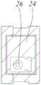
如图5所示,本发明提供的第二实施例,该实施例与第一实施例的区别是,与光学组件24相连的光接口26设置为一个,相应地,适配器与光学组件24的插口也设置为一个。该实施例中,光接口26设置为光收发合一的光接口。当然,光接口26也可以仅设置为光发射接口,或仅设置为光接收接口。其它均与第一实施例相同,在此不再做详细赘述。As shown in Figure 5, the second embodiment provided by the present invention, the difference between this embodiment and the first embodiment is that the
如图6至图8所示,本发明提供的第三实施例,该实施例与第一实施例的区别是,适配器36和壳体的连接部其中之一上设有第一缺口32,第一缺口32内填充有将适配器36和壳体的连接部固定在一起的固定胶。具体到本实施例中,壳体的连接部上设有第一缺口32,具体的,壳体的侧壁35上设有第一缺口32,当将壳体与适配器36插接于一起后,在第一缺口内填充入固定胶,从而使得适配器36和壳体的固定更加可靠。As shown in Figures 6 to 8, the present invention provides a third embodiment. The difference between this embodiment and the first embodiment is that one of the connection parts between the
第一缺口32的开口方向垂直于壳体相对于适配器36的插接方向。具体的,第一缺口32位于下壳体30上,第一缺口32的开口方向朝向上壳体34。本实施例中,第一缺口32为U形。当然,第一缺口32也可设置为L形、圆形、椭圆形或多边形等其它形状。The opening direction of the
优选的,第一缺口32设置为两个,且两个第一缺口32对称位于在适配器36的两侧。当然,两个第一缺口32也可以采用不对称设置。另外,第一缺口32的开口也可以设置成背对上壳体34设置,即设置在下壳体30背对上壳体34的一侧设置。该实施例其它部分与第一实施例相同,在此不再详细介绍。Preferably, there are two
本实施例中,当将适配器36装配于壳体时,待将适配器36调整到所需位置后,在第一缺口32中点胶,从而将适配器36与壳体固定在一起。In this embodiment, when the
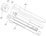
如图9和图10所示,本发明提供的第四实施例,该实施例与第三实施例的区别是,壳体的连接部上设有第一缺口40和第二缺口42,第一缺口40和第二缺口42均用于填入壳体和适配器46之间的固定胶。具体的,第一缺口40和第二缺口42设置于壳体的侧壁35上,当然,也可将第一缺口40和第二缺口42设置于适配器46的连接部上,具体的,第一缺口40和第二缺口42也设置于适配器46的侧壁上。As shown in Figure 9 and Figure 10, the fourth embodiment provided by the present invention, the difference between this embodiment and the third embodiment is that a
本实施例中,第二缺口42和第一缺口40的开口方向相反。具体的,第一缺口40的开口朝向上壳体44,第二缺口42的开口背对上壳体44。In this embodiment, the opening directions of the
优选的,第一缺口40设置为两个,且两个第一缺口40对称位于适配器46的两侧,第二缺口42也设置为两个,且两个第二缺口42也对称位于适配器46的两侧。当然,两个第一缺口40也可以采用不对称设置,同样,两个第二缺口42也可以采用不对称设置。Preferably, there are two
本实施例中,当将适配器46装配于壳体时,待将适配器46调整到所需位置后,在第一缺口40和第二缺口42中点胶,从而将适配器46与壳体固定在一起,且使得适配器46与壳体之间的固定更加牢固。In this embodiment, when the
进一步的,适配器46的连接部上设有凸块48。当然,也可以将凸块48设置于壳体的连接部上。凸块48至少部分位于第一缺口40,凸块48与第一缺口40之间的间隙用固定胶填充,从而进一步加强适配器46的固定。具体的,凸块48也对称设置为两个,两个凸块48分别位于两个第一缺口40中。该实施例其它部分与第一实施例相同,在此不再详细介绍。在其它实施例中,缺口及凸块的形状和个数可以根据需要进行调整,如L形、圆形、椭圆形、U形或多边形等,本发明并不限定缺口和凸块的形状、个数和在侧壁上的位置。缺口和凸起可以是一一对应关系,也可以是多对一关系。需要说明的是,虽然凸块和缺口可以是相互配合的关系,但凸块和缺口并不是紧密配合关系,这样适配器相对于壳体的位置可以微调,调整到位后相互固定,从而可以使光纤连接器和光学组件的光接口完美适配合。避免插拔过紧的现象发生。Further, a
应当理解,虽然本说明书按照实施方式加以描述,但并非每个实施方式仅包含一个独立的技术方案,说明书的这种叙述方式仅仅是为清楚起见,本领域技术人员应当将说明书作为一个整体,各实施方式中的技术方案也可以经适当组合,形成本领域技术人员可以理解的其他实施方式。It should be understood that although this description is described according to implementation modes, not each implementation mode only contains an independent technical solution, and this description in the description is only for clarity, and those skilled in the art should take the description as a whole, and each The technical solutions in the embodiments can also be properly combined to form other embodiments that can be understood by those skilled in the art.
上文所列出的一系列的详细说明仅仅是针对本发明的可行性实施方式的具体说明,它们并非用以限制本发明的保护范围,凡未脱离本发明技艺精神所作的等效实施方式或变更均应包含在本发明的保护范围之内。The series of detailed descriptions listed above are only specific descriptions of the feasible implementation modes of the present invention, and they are not intended to limit the protection scope of the present invention. All changes should be included within the protection scope of the present invention.
Claims (27)
Priority Applications (1)
| Application Number | Priority Date | Filing Date | Title |
|---|---|---|---|
| CN202211414262.3ACN115826159A (en) | 2017-07-19 | 2017-07-19 | Optical module, optical module and assembling method thereof |
Applications Claiming Priority (2)
| Application Number | Priority Date | Filing Date | Title |
|---|---|---|---|
| CN201710591207.4ACN109283633A (en) | 2017-07-19 | 2017-07-19 | Optical module and its assembly method |
| CN202211414262.3ACN115826159A (en) | 2017-07-19 | 2017-07-19 | Optical module, optical module and assembling method thereof |
Related Parent Applications (1)
| Application Number | Title | Priority Date | Filing Date |
|---|---|---|---|
| CN201710591207.4ADivisionCN109283633A (en) | 2017-07-19 | 2017-07-19 | Optical module and its assembly method |
Publications (1)
| Publication Number | Publication Date |
|---|---|
| CN115826159Atrue CN115826159A (en) | 2023-03-21 |
Family
ID=65018916
Family Applications (2)
| Application Number | Title | Priority Date | Filing Date |
|---|---|---|---|
| CN202211414262.3APendingCN115826159A (en) | 2017-07-19 | 2017-07-19 | Optical module, optical module and assembling method thereof |
| CN201710591207.4APendingCN109283633A (en) | 2017-07-19 | 2017-07-19 | Optical module and its assembly method |
Family Applications After (1)
| Application Number | Title | Priority Date | Filing Date |
|---|---|---|---|
| CN201710591207.4APendingCN109283633A (en) | 2017-07-19 | 2017-07-19 | Optical module and its assembly method |
Country Status (2)
| Country | Link |
|---|---|
| US (4) | US10254492B2 (en) |
| CN (2) | CN115826159A (en) |
Families Citing this family (8)
| Publication number | Priority date | Publication date | Assignee | Title |
|---|---|---|---|---|
| CN111736278A (en)* | 2016-04-28 | 2020-10-02 | 苏州旭创科技有限公司 | Optical module |
| CN115826159A (en)* | 2017-07-19 | 2023-03-21 | 苏州旭创科技有限公司 | Optical module, optical module and assembling method thereof |
| JP7480646B2 (en) | 2020-09-07 | 2024-05-10 | 住友電気工業株式会社 | Optical Transceiver |
| CN111999826A (en)* | 2020-09-24 | 2020-11-27 | 武汉锐奥特科技有限公司 | High-precision optical module and assembling method thereof |
| CN111999829A (en)* | 2020-09-24 | 2020-11-27 | 武汉锐奥特科技有限公司 | A kind of embedded optical module and its assembly method |
| CN111999828A (en)* | 2020-09-24 | 2020-11-27 | 武汉锐奥特科技有限公司 | A direct-connected optical module and its assembly method |
| CN115128747A (en)* | 2022-06-20 | 2022-09-30 | 武汉永鼎光通科技有限公司 | Optical module, case thereof, and method for assembling optical module |
| US12302967B1 (en) | 2024-09-04 | 2025-05-20 | Clim8 | Textile element such as a clothing |
Citations (5)
| Publication number | Priority date | Publication date | Assignee | Title |
|---|---|---|---|---|
| US5138679A (en)* | 1991-04-17 | 1992-08-11 | Amp Incorporated | Optical fiber connector with centering and floating alignment feature |
| US20030020986A1 (en)* | 1999-05-27 | 2003-01-30 | Pang Ron Cheng Chuan | Method and apparatus for pluggable fiber optic modules |
| US20130077978A1 (en)* | 2011-09-23 | 2013-03-28 | Tyco Electronics Nederland Bv | Multi-channel transceiver |
| US20140161394A1 (en)* | 2012-12-10 | 2014-06-12 | Applied Optoelectronics, Inc. | Multi-channel optical transceiver module including dual fiber type direct link adapter for optically coupling optical subassemblies in the transceiver module |
| US20170160500A1 (en)* | 2015-12-04 | 2017-06-08 | Hisense Broadband Multimedia Technologies Co., Ltd. | Optical module |
Family Cites Families (11)
| Publication number | Priority date | Publication date | Assignee | Title |
|---|---|---|---|---|
| US5202943A (en)* | 1991-10-04 | 1993-04-13 | International Business Machines Corporation | Optoelectronic assembly with alignment member |
| JP3455168B2 (en)* | 1999-07-19 | 2003-10-14 | 古河電気工業株式会社 | Receptacle module |
| US7350979B2 (en)* | 2004-02-13 | 2008-04-01 | Sumitomo Electric Industries, Ltd. | Optical transceiver having an optical receptacle optionally fixed to a frame |
| US7367720B2 (en)* | 2005-03-15 | 2008-05-06 | Sumitomo Electric Industries, Ltd. | Optical transceiver with optical subassemblies optionally fixed to housing |
| CN101813810B (en) | 2010-03-31 | 2011-07-13 | 河北华美光电子有限公司 | Shell structure for parallel light transceiving module |
| CN103018853A (en)* | 2012-12-06 | 2013-04-03 | 绍兴飞泰光电技术有限公司 | Optical device coupling device |
| WO2015042225A2 (en)* | 2013-09-18 | 2015-03-26 | Fci Asia Pte. Ltd | Optoelectrical connector system |
| CN104503040B (en) | 2014-12-31 | 2016-08-24 | 中航海信光电技术有限公司 | Parallel optical transceiver module |
| JP6805746B2 (en)* | 2016-11-14 | 2020-12-23 | 住友電気工業株式会社 | Optical transceiver |
| US10466427B2 (en)* | 2017-03-14 | 2019-11-05 | Finisar Corporation | Optical module with integrated lens |
| CN115826159A (en)* | 2017-07-19 | 2023-03-21 | 苏州旭创科技有限公司 | Optical module, optical module and assembling method thereof |
- 2017
- 2017-07-19CNCN202211414262.3Apatent/CN115826159A/enactivePending
- 2017-07-19CNCN201710591207.4Apatent/CN109283633A/enactivePending
- 2017-12-22USUS15/852,057patent/US10254492B2/enactiveActive
- 2019
- 2019-04-05USUS16/376,118patent/US11347011B2/enactiveActive
- 2022
- 2022-04-28USUS17/661,076patent/US11803023B2/enactiveActive
- 2023
- 2023-10-20USUS18/491,016patent/US20240045161A1/enactivePending
Patent Citations (6)
| Publication number | Priority date | Publication date | Assignee | Title |
|---|---|---|---|---|
| US5138679A (en)* | 1991-04-17 | 1992-08-11 | Amp Incorporated | Optical fiber connector with centering and floating alignment feature |
| US20030020986A1 (en)* | 1999-05-27 | 2003-01-30 | Pang Ron Cheng Chuan | Method and apparatus for pluggable fiber optic modules |
| US20130077978A1 (en)* | 2011-09-23 | 2013-03-28 | Tyco Electronics Nederland Bv | Multi-channel transceiver |
| CN104246566A (en)* | 2011-09-23 | 2014-12-24 | 泰科电子连接荷兰公司 | multi-channel transceiver |
| US20140161394A1 (en)* | 2012-12-10 | 2014-06-12 | Applied Optoelectronics, Inc. | Multi-channel optical transceiver module including dual fiber type direct link adapter for optically coupling optical subassemblies in the transceiver module |
| US20170160500A1 (en)* | 2015-12-04 | 2017-06-08 | Hisense Broadband Multimedia Technologies Co., Ltd. | Optical module |
Also Published As
| Publication number | Publication date |
|---|---|
| US11347011B2 (en) | 2022-05-31 |
| US20190025530A1 (en) | 2019-01-24 |
| US20190227247A1 (en) | 2019-07-25 |
| US11803023B2 (en) | 2023-10-31 |
| US20220252803A1 (en) | 2022-08-11 |
| US20240045161A1 (en) | 2024-02-08 |
| CN109283633A (en) | 2019-01-29 |
| US10254492B2 (en) | 2019-04-09 |
Similar Documents
| Publication | Publication Date | Title |
|---|---|---|
| CN115826159A (en) | Optical module, optical module and assembling method thereof | |
| CN102549852B (en) | Combined optical and electrical interface | |
| EP2880482B1 (en) | Opto-electronic contact and method | |
| CN105940567B (en) | Pluggable module | |
| CN109407232B (en) | Optical module | |
| US20130109202A1 (en) | Electrical connector for a pluggable transceiver module | |
| CN107329215A (en) | Optical module and its assembly method | |
| TW201404056A (en) | Plug and play optical transceiver module for electronic devices | |
| JP5269613B2 (en) | Photoelectric conversion connection device | |
| WO2013001925A1 (en) | Plug | |
| WO2019095618A1 (en) | Data line male head interface, data line female socket interface, and data line | |
| CN108459383A (en) | A kind of optical coupler module and optical fiber connector | |
| CN103995325B (en) | Optical transceiver module | |
| CN116381869A (en) | Adapter assembly, optical port assembly and optical module | |
| CN111999826A (en) | High-precision optical module and assembling method thereof | |
| CN204631296U (en) | optical connection components | |
| CN104793299B (en) | Combined optical and electrical interface | |
| CN116208837B (en) | Electronic device capable of changing camera module at any time | |
| CN214544470U (en) | Periscopic camera module and electronic equipment | |
| CN215813457U (en) | 200G-CFP2 optical module structure | |
| JP6034778B2 (en) | Input/Output (I/O) Devices | |
| CN202259891U (en) | Connector | |
| CN116626815A (en) | Integral SC connector and use method | |
| CN203398461U (en) | Electric connector component | |
| CN113126209A (en) | Optical waveguide plate, positioner, optical waveguide plate assembly and optical back plate |
Legal Events
| Date | Code | Title | Description |
|---|---|---|---|
| PB01 | Publication | ||
| PB01 | Publication | ||
| SE01 | Entry into force of request for substantive examination | ||
| SE01 | Entry into force of request for substantive examination |