CN115810605A - Lead frame, semiconductor device, inspection method, and lead frame manufacturing method - Google Patents
Lead frame, semiconductor device, inspection method, and lead frame manufacturing methodDownload PDFInfo
- Publication number
- CN115810605A CN115810605ACN202211101067.5ACN202211101067ACN115810605ACN 115810605 ACN115810605 ACN 115810605ACN 202211101067 ACN202211101067 ACN 202211101067ACN 115810605 ACN115810605 ACN 115810605A
- Authority
- CN
- China
- Prior art keywords
- die pad
- lead frame
- hole
- semiconductor chip
- film
- Prior art date
- Legal status (The legal status is an assumption and is not a legal conclusion. Google has not performed a legal analysis and makes no representation as to the accuracy of the status listed.)
- Pending
Links
Images


Classifications
- H—ELECTRICITY
- H01—ELECTRIC ELEMENTS
- H01L—SEMICONDUCTOR DEVICES NOT COVERED BY CLASS H10
- H01L23/00—Details of semiconductor or other solid state devices
- H01L23/48—Arrangements for conducting electric current to or from the solid state body in operation, e.g. leads, terminal arrangements ; Selection of materials therefor
- H01L23/488—Arrangements for conducting electric current to or from the solid state body in operation, e.g. leads, terminal arrangements ; Selection of materials therefor consisting of soldered or bonded constructions
- H01L23/495—Lead-frames or other flat leads
- H01L23/49503—Lead-frames or other flat leads characterised by the die pad
- H01L23/49513—Lead-frames or other flat leads characterised by the die pad having bonding material between chip and die pad
- H—ELECTRICITY
- H01—ELECTRIC ELEMENTS
- H01L—SEMICONDUCTOR DEVICES NOT COVERED BY CLASS H10
- H01L22/00—Testing or measuring during manufacture or treatment; Reliability measurements, i.e. testing of parts without further processing to modify the parts as such; Structural arrangements therefor
- H01L22/30—Structural arrangements specially adapted for testing or measuring during manufacture or treatment, or specially adapted for reliability measurements
- G—PHYSICS
- G01—MEASURING; TESTING
- G01B—MEASURING LENGTH, THICKNESS OR SIMILAR LINEAR DIMENSIONS; MEASURING ANGLES; MEASURING AREAS; MEASURING IRREGULARITIES OF SURFACES OR CONTOURS
- G01B11/00—Measuring arrangements characterised by the use of optical techniques
- G01B11/26—Measuring arrangements characterised by the use of optical techniques for measuring angles or tapers; for testing the alignment of axes
- G01B11/27—Measuring arrangements characterised by the use of optical techniques for measuring angles or tapers; for testing the alignment of axes for testing the alignment of axes
- G01B11/272—Measuring arrangements characterised by the use of optical techniques for measuring angles or tapers; for testing the alignment of axes for testing the alignment of axes using photoelectric detection means
- H—ELECTRICITY
- H01—ELECTRIC ELEMENTS
- H01L—SEMICONDUCTOR DEVICES NOT COVERED BY CLASS H10
- H01L21/00—Processes or apparatus adapted for the manufacture or treatment of semiconductor or solid state devices or of parts thereof
- H01L21/02—Manufacture or treatment of semiconductor devices or of parts thereof
- H01L21/04—Manufacture or treatment of semiconductor devices or of parts thereof the devices having potential barriers, e.g. a PN junction, depletion layer or carrier concentration layer
- H01L21/48—Manufacture or treatment of parts, e.g. containers, prior to assembly of the devices, using processes not provided for in a single one of the groups H01L21/18 - H01L21/326 or H10D48/04 - H10D48/07
- H01L21/4814—Conductive parts
- H01L21/4821—Flat leads, e.g. lead frames with or without insulating supports
- H01L21/4825—Connection or disconnection of other leads to or from flat leads, e.g. wires, bumps, other flat leads
- H—ELECTRICITY
- H01—ELECTRIC ELEMENTS
- H01L—SEMICONDUCTOR DEVICES NOT COVERED BY CLASS H10
- H01L21/00—Processes or apparatus adapted for the manufacture or treatment of semiconductor or solid state devices or of parts thereof
- H01L21/02—Manufacture or treatment of semiconductor devices or of parts thereof
- H01L21/04—Manufacture or treatment of semiconductor devices or of parts thereof the devices having potential barriers, e.g. a PN junction, depletion layer or carrier concentration layer
- H01L21/48—Manufacture or treatment of parts, e.g. containers, prior to assembly of the devices, using processes not provided for in a single one of the groups H01L21/18 - H01L21/326 or H10D48/04 - H10D48/07
- H01L21/4814—Conductive parts
- H01L21/4821—Flat leads, e.g. lead frames with or without insulating supports
- H01L21/4842—Mechanical treatment, e.g. punching, cutting, deforming, cold welding
- H—ELECTRICITY
- H01—ELECTRIC ELEMENTS
- H01L—SEMICONDUCTOR DEVICES NOT COVERED BY CLASS H10
- H01L21/00—Processes or apparatus adapted for the manufacture or treatment of semiconductor or solid state devices or of parts thereof
- H01L21/02—Manufacture or treatment of semiconductor devices or of parts thereof
- H01L21/04—Manufacture or treatment of semiconductor devices or of parts thereof the devices having potential barriers, e.g. a PN junction, depletion layer or carrier concentration layer
- H01L21/50—Assembly of semiconductor devices using processes or apparatus not provided for in a single one of the groups H01L21/18 - H01L21/326 or H10D48/04 - H10D48/07 e.g. sealing of a cap to a base of a container
- H01L21/56—Encapsulations, e.g. encapsulation layers, coatings
- H01L21/565—Moulds
- H—ELECTRICITY
- H01—ELECTRIC ELEMENTS
- H01L—SEMICONDUCTOR DEVICES NOT COVERED BY CLASS H10
- H01L23/00—Details of semiconductor or other solid state devices
- H01L23/48—Arrangements for conducting electric current to or from the solid state body in operation, e.g. leads, terminal arrangements ; Selection of materials therefor
- H01L23/488—Arrangements for conducting electric current to or from the solid state body in operation, e.g. leads, terminal arrangements ; Selection of materials therefor consisting of soldered or bonded constructions
- H01L23/495—Lead-frames or other flat leads
- H01L23/49503—Lead-frames or other flat leads characterised by the die pad
- H—ELECTRICITY
- H01—ELECTRIC ELEMENTS
- H01L—SEMICONDUCTOR DEVICES NOT COVERED BY CLASS H10
- H01L23/00—Details of semiconductor or other solid state devices
- H01L23/48—Arrangements for conducting electric current to or from the solid state body in operation, e.g. leads, terminal arrangements ; Selection of materials therefor
- H01L23/488—Arrangements for conducting electric current to or from the solid state body in operation, e.g. leads, terminal arrangements ; Selection of materials therefor consisting of soldered or bonded constructions
- H01L23/495—Lead-frames or other flat leads
- H01L23/49517—Additional leads
- H01L23/4952—Additional leads the additional leads being a bump or a wire
- H—ELECTRICITY
- H01—ELECTRIC ELEMENTS
- H01L—SEMICONDUCTOR DEVICES NOT COVERED BY CLASS H10
- H01L23/00—Details of semiconductor or other solid state devices
- H01L23/48—Arrangements for conducting electric current to or from the solid state body in operation, e.g. leads, terminal arrangements ; Selection of materials therefor
- H01L23/488—Arrangements for conducting electric current to or from the solid state body in operation, e.g. leads, terminal arrangements ; Selection of materials therefor consisting of soldered or bonded constructions
- H01L23/495—Lead-frames or other flat leads
- H01L23/49575—Assemblies of semiconductor devices on lead frames
- G—PHYSICS
- G01—MEASURING; TESTING
- G01B—MEASURING LENGTH, THICKNESS OR SIMILAR LINEAR DIMENSIONS; MEASURING ANGLES; MEASURING AREAS; MEASURING IRREGULARITIES OF SURFACES OR CONTOURS
- G01B11/00—Measuring arrangements characterised by the use of optical techniques
- G01B11/002—Measuring arrangements characterised by the use of optical techniques for measuring two or more coordinates
- H—ELECTRICITY
- H01—ELECTRIC ELEMENTS
- H01L—SEMICONDUCTOR DEVICES NOT COVERED BY CLASS H10
- H01L21/00—Processes or apparatus adapted for the manufacture or treatment of semiconductor or solid state devices or of parts thereof
- H01L21/02—Manufacture or treatment of semiconductor devices or of parts thereof
- H01L21/04—Manufacture or treatment of semiconductor devices or of parts thereof the devices having potential barriers, e.g. a PN junction, depletion layer or carrier concentration layer
- H01L21/50—Assembly of semiconductor devices using processes or apparatus not provided for in a single one of the groups H01L21/18 - H01L21/326 or H10D48/04 - H10D48/07 e.g. sealing of a cap to a base of a container
- H01L21/56—Encapsulations, e.g. encapsulation layers, coatings
- H01L21/561—Batch processing
- H—ELECTRICITY
- H01—ELECTRIC ELEMENTS
- H01L—SEMICONDUCTOR DEVICES NOT COVERED BY CLASS H10
- H01L22/00—Testing or measuring during manufacture or treatment; Reliability measurements, i.e. testing of parts without further processing to modify the parts as such; Structural arrangements therefor
- H01L22/10—Measuring as part of the manufacturing process
- H01L22/12—Measuring as part of the manufacturing process for structural parameters, e.g. thickness, line width, refractive index, temperature, warp, bond strength, defects, optical inspection, electrical measurement of structural dimensions, metallurgic measurement of diffusions
- H—ELECTRICITY
- H01—ELECTRIC ELEMENTS
- H01L—SEMICONDUCTOR DEVICES NOT COVERED BY CLASS H10
- H01L23/00—Details of semiconductor or other solid state devices
- H01L23/28—Encapsulations, e.g. encapsulating layers, coatings, e.g. for protection
- H01L23/31—Encapsulations, e.g. encapsulating layers, coatings, e.g. for protection characterised by the arrangement or shape
- H01L23/3107—Encapsulations, e.g. encapsulating layers, coatings, e.g. for protection characterised by the arrangement or shape the device being completely enclosed
Landscapes
- Engineering & Computer Science (AREA)
- Physics & Mathematics (AREA)
- General Physics & Mathematics (AREA)
- Computer Hardware Design (AREA)
- Microelectronics & Electronic Packaging (AREA)
- Power Engineering (AREA)
- Condensed Matter Physics & Semiconductors (AREA)
- Manufacturing & Machinery (AREA)
- Lead Frames For Integrated Circuits (AREA)
Abstract
Description
Translated fromChinese技术领域technical field
本发明涉及引线框架、半导体装置、检查方法及引线框架的制造方法。The present invention relates to a lead frame, a semiconductor device, an inspection method, and a manufacturing method of the lead frame.
背景技术Background technique
近年来,已知有一种半导体装置,其将例如IC(Integrated Circuit,集成电路)芯片等半导体芯片搭载于金属制的引线框架。即,例如将半导体芯片搭载在设于引线框架中央的面状芯片垫上,该半导体芯片例如通过引线键合(wire bonding)与设于芯片垫周围的多个引脚连接。并且,有时对搭载于引线框架的半导体芯片使用例如环氧树脂等树脂进行封装,从而形成半导体装置。In recent years, there has been known a semiconductor device in which a semiconductor chip such as an IC (Integrated Circuit) chip is mounted on a metal lead frame. That is, for example, a semiconductor chip is mounted on a planar die pad provided in the center of a lead frame, and the semiconductor chip is connected to a plurality of pins provided around the die pad by, for example, wire bonding. In addition, a semiconductor chip mounted on a lead frame may be packaged using a resin such as epoxy resin to form a semiconductor device.
搭载于芯片垫上的半导体芯片有时例如通过胶带粘接在芯片垫上。即,在面状的芯片垫上粘贴有具有粘性的胶带,并由胶带粘接半导体芯片,从而将半导体芯片搭载于芯片垫。通过使用例如绝缘性的胶带来将半导体芯片搭载于芯片垫上,能够使半导体芯片与芯片垫电气绝缘。A semiconductor chip mounted on a die pad may be bonded to the die pad with, for example, an adhesive tape. That is, an adhesive tape is pasted on the planar die pad, and the semiconductor chip is bonded by the tape to mount the semiconductor chip on the die pad. By mounting the semiconductor chip on the die pad using, for example, an insulating tape, the semiconductor chip and the die pad can be electrically insulated.
专利文献1:日本特开平8-222585号公报Patent Document 1: Japanese Patent Application Laid-Open No. 8-222585
专利文献2:日本特开昭63-249341号公报Patent Document 2: Japanese Patent Application Laid-Open No. 63-249341
专利文献3:日本特开平1-147836号公报Patent Document 3: Japanese Patent Application Laid-Open No. 1-147836
发明内容Contents of the invention
在使用胶带来将半导体芯片搭载于芯片垫的情况下,半导体芯片的位置取决于胶带所粘贴的位置。因此,将胶带粘贴在芯片垫的适当的位置上非常重要,优选为在制造引线框架后,对胶带是否粘贴在芯片垫的适当的位置上进行检查。When mounting a semiconductor chip on a die pad using an adhesive tape, the position of the semiconductor chip depends on the position where the tape is attached. Therefore, it is very important to stick the tape on the proper position of the die pad, and it is preferable to check whether the tape is pasted on the proper position of the die pad after manufacturing the lead frame.
作为检查胶带位置的方法,存在使用透射光的方法以及使用反射光的方法。即,对粘贴有胶带的引线框架照射光,并在由透射光或反射光生成的图像中检测胶带的位置,由此,能够判断胶带的位置是否适当。As a method of checking the position of the tape, there are a method using transmitted light and a method using reflected light. That is, by irradiating light to the lead frame to which the tape is attached, and detecting the position of the tape in an image generated by transmitted light or reflected light, it is possible to determine whether the position of the tape is appropriate.
然而,对于粘贴在芯片垫上的胶带,存在难以使用透射光或反射光来检测位置是否适当的问题。具体而言,由于芯片垫是光无法穿过的面状的部分,因此在使用透射光来进行检查时,无法检测到粘贴于芯片垫上的胶带。因此,使用透射光的方法难以用于检查粘贴于芯片垫上的胶带的位置是否适当。However, for the tape attached to the die pad, there is a problem that it is difficult to detect whether the position is proper using transmitted light or reflected light. Specifically, since the die pad is a planar portion through which light cannot pass, the tape affixed to the die pad cannot be detected when inspection is performed using transmitted light. Therefore, the method using transmitted light is difficult to be used for checking the proper position of the tape pasted on the die pad.
另外,在使用反射光进行的检查中,与周围的金属部分相比,在胶带位置上的光的反射被抑制,因此能够检测到胶带的位置。然而,由于芯片垫表面的细微的损伤或色调的不均匀等也会使光的反射被抑制,因此根据芯片垫表面的状态而有时无法辨别金属部分与胶带,从而难以准确地检测出胶带的位置。其结果,存在无法确认到胶带所粘贴的位置是否适当,使得搭载于芯片垫上的半导体芯片的位置精准度下降的情况。In addition, in the inspection using reflected light, reflection of light at the tape position is suppressed compared with surrounding metal parts, so the tape position can be detected. However, since reflection of light is also suppressed due to slight damage or uneven color tone on the surface of the die pad, depending on the state of the surface of the die pad, it may not be possible to distinguish between the metal part and the tape, making it difficult to accurately detect the position of the tape. . As a result, it may not be possible to check whether the position where the tape is pasted is appropriate, and the positional accuracy of the semiconductor chip mounted on the die pad may decrease.
所公开的技术是鉴于上述问题而提出的,其目的在于提供一种能够防止半导体芯片的位置精准度下降的引线框架、半导体装置、检查方法及引线框架的制造方法。The disclosed technology is proposed in view of the above problems, and an object thereof is to provide a lead frame, a semiconductor device, an inspection method, and a manufacturing method of the lead frame capable of preventing a decrease in positional accuracy of a semiconductor chip.
本发明公开的引线框架在一个形态中包括:具有半导体芯片的搭载面的芯片垫、以及设于所述芯片垫的搭载面的薄膜状部件,所述芯片垫具有贯穿孔,所述贯穿孔形成于包含所述薄膜状部件的外周的区域。In one aspect, the lead frame disclosed in the present invention includes: a die pad having a mounting surface of a semiconductor chip; In the region including the outer periphery of the film-like member.
根据本发明公开的引线框架、半导体装置、检查方法及引线框架的制造方法的一个形态,能够取得防止半导体芯片的位置精准度下降的效果。According to one aspect of the lead frame, the semiconductor device, the inspection method, and the manufacturing method of the lead frame disclosed in the present invention, it is possible to obtain an effect of preventing a decrease in the positional accuracy of the semiconductor chip.
附图说明Description of drawings
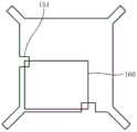
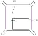
图1是表示一实施方式涉及的引线框架的结构的俯视图。FIG. 1 is a plan view showing the structure of a lead frame according to one embodiment.
图2是用于说明贯穿孔的位置的图。FIG. 2 is a diagram for explaining positions of through holes.
图3(a)至图3(d)是表示贯穿孔的位置的具体示例的图。3(a) to 3(d) are diagrams showing specific examples of the positions of the through holes.
图4(a)至图4(d)是表示胶带的结构的具体示例的图。4(a) to 4(d) are diagrams showing specific examples of the structure of the adhesive tape.
图5是表示引线框架的制造方法的流程图。FIG. 5 is a flowchart showing a method of manufacturing a lead frame.
图6是表示引线框架成形工序的具体示例的图。FIG. 6 is a diagram showing a specific example of a lead frame forming step.
图7是表示电镀加工工序的具体示例的图。FIG. 7 is a diagram showing a specific example of the electroplating process.
图8是表示胶带粘贴工序的具体示例的图。FIG. 8 is a diagram showing a specific example of the tape sticking process.
图9是表示引线框架的检查方法的流程图。FIG. 9 is a flowchart showing a method of inspecting a lead frame.
图10(a)、图10(b)是表示二值图像的具体示例的图。10(a) and 10(b) are diagrams showing specific examples of binary images.
图11是表示半导体装置的制造方法的流程图。FIG. 11 is a flowchart showing a method of manufacturing a semiconductor device.
图12是表示半导体芯片搭载工序的具体示例的图。FIG. 12 is a diagram showing a specific example of a semiconductor chip mounting process.
图13(a)至图13(c)是用于说明粘接半导体芯片的图。13(a) to 13(c) are diagrams for explaining bonding of semiconductor chips.
图14是表示引线键合工序的具体示例的图。FIG. 14 is a diagram showing a specific example of a wire bonding process.
图15是表示树脂封装工序的具体示例的图。FIG. 15 is a diagram showing a specific example of the resin sealing step.
图16是表示分割工序的具体示例的图。FIG. 16 is a diagram showing a specific example of the dividing step.
符号说明Symbol Description
110 框体110 frame
120 引脚120 pins
121 内引脚121 internal pins
122 外引脚122 external pins
125 镀层125 plating
130 支承杆130 support rod
140 连筋140 Ribs
150 芯片垫150 chip pads
151 贯穿孔151 through hole
160 胶带160 Tape
210、215 半导体芯片210, 215 semiconductor chips
230 模塑树脂230 molding resin
具体实施方式Detailed ways
下面,参照附图对本发明公开的引线框架、半导体装置、检查方法及引线框架的制造方法的一实施方式进行详细说明。此外,本发明不限于该实施方式。Hereinafter, one embodiment of the lead frame, semiconductor device, inspection method, and lead frame manufacturing method disclosed in the present invention will be described in detail with reference to the accompanying drawings. In addition, the present invention is not limited to this embodiment.
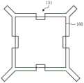
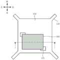
图1是表示一实施方式涉及的引线框架100的结构的俯视图。由于引线框架100是作为由多个引线框架100连结而成的集合体来制造的,在图1中,对集合体中的一个引线框架100进行图示。FIG. 1 is a plan view showing the structure of a
引线框架100具有:框体110、引脚120、支承杆130、连筋(dam bar)140及芯片垫150。引线框架100例如由厚度为0.1~0.25mm左右的铜或铜合金等金属板形成。The
框体110对一个引线框架100的外周进行划定,并对引脚120、支承杆130及芯片垫150进行支承。在制造引线框架100时,引线框架100作为通过框体110连结多个引线框架100的集合体被制造。并且,在引线框架100搭载了半导体芯片并被树脂封装后,将引脚120间的连筋140切断,并将包括引脚120、支承杆130及芯片垫150的部分从框体110切开,则能够得到被分割成单片的半导体装置。The
在引线框架100搭载有半导体芯片的情况下,引脚120形成将该半导体芯片与外部部件电气连接的端子。即,在引线框架100搭载有半导体芯片的情况下,半导体芯片例如通过引线键合与引脚120连接。在引线框架100中,形成有包围芯片垫150的多个引脚120,相邻的引脚120通过连筋140连接。When a semiconductor chip is mounted on the
此外,引脚120包括内引脚121和外引脚122。内引脚121形成于比连筋140靠近芯片垫150处,与搭载于芯片垫150的半导体芯片电气连接。外引脚122形成于比连筋140远离芯片垫150处,成为与外部部件电气连接的端子。在搭载于芯片垫150的半导体芯片被树脂封装时,内引脚121与半导体芯片一起被树脂封装,而外引脚122从树脂中露出。In addition, the
支承杆130将框体110与芯片垫150连接,用于支承芯片垫150。在搭载于芯片垫150的半导体芯片被树脂封装时,支承杆130与半导体芯片一起被树脂封装。并且,在经过树脂封装后,支承杆130被从框体110切开。The supporting
连筋140连接平行排列的多个引脚120,并将这些多个引脚120连接于框体110。通过在搭载于芯片垫150的半导体芯片被树脂封装后切断连筋140,使得连筋140连接的引脚120被各自分离。The connecting
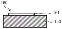
芯片垫150是形成于引线框架100中央的面状的区域,例如通过四个支承杆130与框体110连结。芯片垫150具有例如一个边为2~20mm左右的正方形或长方形的面,半导体芯片被搭载于该面上。具体而言,在芯片垫150上粘贴有胶带160,半导体芯片粘接于胶带160的位置。并且,在包含胶带160的外周一部分的区域中,形成有将芯片垫150贯穿的贯穿孔151,所述胶带160被粘贴于芯片垫150的适当的位置。即,若胶带160被粘贴于芯片垫150的适当的位置上,则该胶带160的外周一部分位于贯穿孔151内。在图1所示的示例中,胶带160的对角的顶点均位于贯穿孔151内。The
在此,参照图2对贯穿孔151的位置进行说明。图2示意性地表示芯片垫150的形状,图2的下图是放大表示贯穿孔151的周围的图。Here, the position of the through
如图2所示,芯片垫150例如在两处形成有贯穿孔151。各贯穿孔151形成为包含,在胶带160被粘贴在适当的位置的情况下顶点160a可能存在的范围,该顶点160a作为表示胶带160的位置的基准点。即,贯穿孔151形成为作为基准点的顶点160a可能存在的预设范围以上的大小。As shown in FIG. 2 , for example, two through
具体而言,如图2的下图所示,贯穿孔151的前端位于:在胶带160被粘贴于适当的位置的范围内的最前方的情况下的顶点160a的位置的前方,贯穿孔151的后端位于:在胶带160被粘贴于适当的位置的范围内的最后方的情况下的顶点160a的位置的后方。同样地,贯穿孔151的左端位于:在胶带160被粘贴于适当的位置的范围内的最左方的情况下的顶点160a的位置的左方,贯穿孔151的右端位于:在胶带160被粘贴于适当的位置的范围内的最右方的情况下的顶点160a的位置的右方。如此,贯穿孔151形成为与胶带160的粘贴位置可容许的误差范围对应的大小,例如具有一个边为0.4~2mm左右的正方形形状或长方形形状。Specifically, as shown in the lower figure of FIG. 2 , the front end of the through
如此,贯穿孔151在胶带160被粘贴于适当的位置时的胶带160的基准点可能存在的区域,贯穿芯片垫150。由此,当胶带160被粘贴于适当的位置时,作为胶带160的基准点的顶点160a位于贯穿孔151内。因此,在对芯片垫150照射光时,能够由穿过贯穿孔151的透射光生成能够检测出胶带160的基准点的坐标的图像,从而能够检查胶带160是否被粘贴在适当的位置上。In this way, the through
此外,图1、图2表示了将胶带160的对角的顶点作为基准点的情况下的贯穿孔151的位置,但贯穿孔151的位置不限于此。具体而言,例如如图3(a)所示,在将胶带160的对角的顶点作为基准点的情况下,贯穿孔151也可以与芯片垫150的外周相接。即,在图3(a)所示的示例中,贯穿孔151形成为切开芯片垫150的外周的形状。1 and 2 show the position of the through
此外,在胶带160被粘贴于整个芯片垫150的情况下,例如如图3(b)所示,可以将胶带160的外周四个边作为基准线,在芯片垫150的外周四个边上形成贯穿孔151。即,在图3(b)所示的示例中,贯穿孔151形成为切开芯片垫150的外周四个边的形状,当胶带160被粘贴于适当的位置时,胶带160的四个边位于贯穿孔151内。In addition, when the
此外,例如如图3(c)所示,也可以将胶带160的外周四个边作为基准线,而在芯片垫150上形成四处贯穿孔151。这种情况下,当胶带160被粘贴于适当的位置时,胶带160的四个边也位于贯穿孔151内。In addition, for example, as shown in FIG. 3( c ), it is also possible to form four through
进一步地,例如如图3(d)所示,也可以将胶带160的一个顶点作为基准点,而在芯片垫150上形成一处贯穿孔151。这种情况下,当胶带160被粘贴于适当的位置时,作为胶带160的基准点的顶点位于贯穿孔151内。Further, for example, as shown in FIG. 3( d ), a through
此外,形成贯穿孔151的位置是根据在芯片垫150上粘贴的胶带160的位置来决定的,为了将半导体芯片通过胶带160可靠地接合于芯片垫150上,优选使贯穿孔151形成于俯视视角下与半导体芯片不重叠的位置。通过配合贯穿孔151的形成位置对胶带160的大小进行调整,则可以以覆盖半导体芯片的搭载范围且基准点位于贯穿孔151内的方式粘贴胶带160。此外,贯穿孔151形成为,具有大于等于胶带160的基准点(线)可能存在的预设范围的大小的各种形状即可。因此,例如除正方形及长方形等矩形以外,贯穿孔151的形状也可以是各种多边形、圆形或椭圆形等。In addition, the position where the through
胶带160是能够被粘贴在芯片垫150的表面的薄膜状部件。胶带160具有在俯视视角下,例如一个边为1~20mm左右的正方形形状或长方形形状,并且胶带160被粘贴在芯片垫150的搭载半导体芯片的位置。若胶带160被粘贴于预定搭载半导体芯片的适当的位置,则胶带160的预设的顶点或边等基准点或基准线位于贯穿孔151内。胶带160的结构的具体示例如图4(a)~图4(d)所示。图4(b)~图4(d)表示图4(a)的I-I线截面。The
如图4(b)所示,胶带160例如可以由一层粘接层161形成。即,胶带160可以是由粘接材料构成的粘接层161被粘贴在芯片垫150上的胶带。粘接层161例如可以使用环氧树脂等绝缘树脂来形成。粘接层161的厚度例如可以为10~100μm左右。由于这种胶带160是由一层粘接层161形成的,因此胶带160的两个面具有粘性,其一个面可以被粘贴在芯片垫150上,同时另一个面可以与半导体芯片粘接。As shown in FIG. 4( b ), the
此外,如图4(c)所示,胶带160例如可以为在基材层162的一个面上层叠粘接层161的双层结构。即,胶带160可以是将层叠在基材层162上的粘接层161粘贴在芯片垫150上的胶带。基材层162例如可以使用聚酰亚胺树脂等绝缘树脂来形成。粘接层161的厚度例如可以为10~50μm左右,基材层162的厚度例如可以为50~100μm左右。因此,胶带160的厚度例如为60~150μm左右。在这种胶带160中,由于基材层162的一个面上层叠有粘接层161,因此胶带160的粘接层161侧的面被粘贴在芯片垫150上。在该胶带160上搭载半导体芯片时,通过在基材层162的表面形成粘接层来粘接半导体芯片。In addition, as shown in FIG. 4( c ), the
此外,如图4(d)所示,胶带160例如还可以为在基材层162的两个面上层叠粘接层161、163的三层结构。即,胶带160还可以是层叠于基材层162的粘接层161被粘贴于芯片垫150、并且粘接层163露出于表面的胶带。粘接层163与粘接层161一样地,例如可以使用环氧树脂等绝缘树脂来形成。粘接层161、163的厚度例如均可以为10~50μm左右,基材层162的厚度例如可以为50~100μm左右。因此,胶带160的厚度例如为70~200μm左右。在这种胶带160中,由于在胶带160的两个面形成有粘接层161、163,使得粘接层161能够被粘贴于芯片垫150,且粘接层163能够与半导体芯片粘接。In addition, as shown in FIG. 4( d ), the
像这样,由于可以在芯片垫150上粘贴各种结构的胶带160,通过适当地选择具有所需厚度的胶带160,则能够调整芯片垫150与粘接在胶带160上的半导体芯片之间的距离。Like this, since the
接下来,参照图5所示的流程图来对如上所述构成的引线框架100的制造方法进行说明。Next, a method of manufacturing the
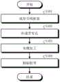
首先,通过对例如厚度为0.1~0.25mm左右的铜或铜合金等金属板进行冲压加工或蚀刻等处理,来成形引线框架100(步骤S101)。此外,在成形引线框架100的同时,在芯片垫150上形成贯穿孔151(步骤S102)。具体而言,例如如图6所示,通过冲压加工或蚀刻处理将金属板的不要的部分去除,由此,在被框体110包围的区域内,形成引脚120、支承杆130、连筋140及芯片垫150。并且,在芯片垫150中形成贯穿孔151。First, the
然后,对构成引脚120的内引脚121施加电镀加工(步骤S103)。即,例如如图7所示,在内引脚121的连接金属丝的位置形成镀层125。镀层125例如通过镀银形成。此外,在图7、图8以外的附图中,省略镀层125的图示。Then, plating is applied to the
在形成镀层125后,将胶带160粘贴在芯片垫150上(步骤S104)。具体而言,胶带160通过将胶带160的粘接层161粘接于芯片垫150的搭载半导体芯片的位置来完成粘贴。此时,如图8所示,只要胶带160被粘贴在适当的位置,则胶带160的预设的顶点或边等基准点或基准线位于贯穿孔151内。After the
通过以上的工序,则完成了能够将半导体芯片搭载于粘贴在芯片垫150的胶带160上的引线框架100的制作。由于芯片垫150中的半导体芯片的位置取决于胶带160的位置,因此胶带160需要被粘贴在适当的位置上。由于通过上述工序制造的引线框架100的芯片垫150上形成有贯穿孔151,因此能够高效地检查胶带160是否被粘贴在适当的位置上。Through the above steps, the fabrication of the
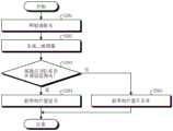
图9是表示引线框架100的检查方法的流程图。引线框架100的检查例如通过具备光源、光传感器及图像处理装置的检查装置来执行。FIG. 9 is a flowchart showing a method of inspecting the
在芯片垫150上粘贴有胶带160的引线框架100制作完成后,从光源向引线框架100照射穿过贯穿孔151的透射光(步骤S201)。即,光传感器隔着引线框架100被配置在光源的相反侧,来自光源的光被框体110、引脚120、支承杆130、连筋140及芯片垫150遮挡,而仅从包含芯片垫150的贯穿孔151在内的空隙部分穿过。然后,通过光传感器能够检测到穿过引线框架100的空隙部分的透射光。在光传感器检测到透射光后,生成表示遮挡了光的区域和穿过了光的区域的二值图像(步骤S202)。After the
然后,在二值图像中确定与芯片垫150的贯穿孔151对应的区域,并在该区域内检测胶带160的基准点或基准线的坐标。具体而言,在二值图像的对应贯穿孔151的区域中确定被胶带160遮挡了光的区域,从而检测到与该胶带160对应的区域的预设顶点或预设边等的坐标。像这样,只要胶带160的基准点或基准线位于贯穿孔151内,则能够在二值图像中检测到胶带160的基准点或基准线的坐标。然后,对检测到的基准点或基准线的坐标是否包含于与胶带160的适当粘贴位置对应的预设范围内进行判断(步骤S203)。即,对基准点或基准线是否位于以可容许的误差粘贴胶带160时的范围内进行判断。Then, a region corresponding to the through-
作为该判断的结果,当胶带160的基准点或基准线在预设范围内时(步骤S203:是),判定胶带160被粘贴于适当的位置(步骤S204)。另一方面,当胶带160的基准点或基准线不在预设范围内时(步骤S203:否),判定胶带160未被粘贴于适当的位置(步骤S205)。As a result of this determination, when the reference point or reference line of the
具体而言,例如如图10(a)所示,在二值图像中,贯穿孔151区域内的一部分是与遮挡了光的胶带160对应的区域,在作为胶带160的基准点的顶点160a的坐标包含于预设范围内的情况下,判定胶带160的位置适当。另一方面,即使作为胶带160的基准点的顶点160a包含于贯穿孔151的区域内,在顶点160a的坐标不包含于预设范围内的情况下,判定胶带160的位置不正常。此外,例如如图10(b)所示,在二值图像中,贯穿孔151的全部区域为被光穿过的区域时,作为胶带160的基准点的顶点160a不包含于贯穿孔151的区域内,因此判定胶带160的位置不正常。进一步地,在二值图像中贯穿孔151的全部区域为遮挡了光的区域的情况下,由于作为胶带160的基准点的顶点160a不包含于贯穿孔151的区域内,因此也判定胶带160的位置不正常。Specifically, for example, as shown in FIG. 10( a ), in the binary image, a part of the region of the through
像这样,通过使贯穿孔151形成于,包含被粘贴在芯片垫150中的适当位置的胶带160的外周一部分的区域,则能够使用透射光来检测胶带160的基准点或基准线的坐标,从而能够检查胶带160是否被粘贴于适当的位置。In this way, by forming the through
接下来,参照图11所示的流程图对使用引线框架100构成的半导体装置的制造方法进行说明。用于制造半导体装置的引线框架100为,通过上述的检查,被判定为胶带160已粘贴于芯片垫150的适当的位置的引线框架。Next, a method of manufacturing a semiconductor device configured using the
将半导体芯片搭载于引线框架100的芯片垫150上(步骤S301)。具体而言,例如如图12所示,将半导体芯片210粘接于胶带160的位置上。此外,在芯片垫150上,除了通过胶带160粘接的半导体芯片210,例如还可以搭载通过焊料或芯片粘贴膏等接合的半导体芯片215。A semiconductor chip is mounted on the
通过胶带160粘接的半导体芯片210的大小为在俯视视角下收纳在胶带160的范围内的大小,半导体芯片210的整个面与胶带160粘接。此时,例如如图13(a)所示,在胶带160是由一层的粘接层161形成的情况下,半导体芯片210直接被粘接在粘接层161上。此外,例如如图13(b)所示,在胶带160为粘接层161及基材层162的双层结构的情况下,基材层162的表面形成有粘接层211,而半导体芯片210被粘接在粘接层211上。并且,例如如图13(c)所示,在胶带160为粘接层161、基材层162及粘接层163的三层结构的情况下,半导体芯片210被粘接在粘接层163上。The size of the
在将半导体芯片210搭载在芯片垫150上后,通过引线键合将引脚120与半导体芯片210电气连接(步骤S302)。此外,在芯片垫150上搭载有多个半导体芯片210、215的情况下,各个半导体芯片210、215之间可以通过引线键合连接。具体而言,例如如图14所示,内引脚121的镀层125与半导体芯片210的端子通过金属丝220连接。此外,相邻的半导体芯片210、215的端子之间也通过金属丝220来连接。After the
然后,例如使用环氧树脂等模塑树脂将半导体芯片210、215封装(步骤S303)。具体而言,搭载有半导体芯片210、215的芯片垫150、内引脚121及支承杆130例如被图15中虚线所示的范围内的模塑树脂230封装。Then, the
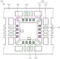
在将半导体芯片210、215树脂封装后,将引脚120及支承杆130从框体110切开,并且将连接相邻的引脚120之间的连筋140切断。由此,得到分割成单片的半导体装置,制成使用了引线框架100的半导体装置(步骤S304)。该半导体装置例如如图16所示,具有外引脚122向模塑树脂230的外侧突出的形状。这些外引脚122成为与外部连接的端子。After the
如上所述,根据本实施方式,在引线框架的芯片垫上粘贴有用于粘接半导体芯片的胶带,并在包含被粘贴在适当的位置时的胶带的外周一部分的区域,形成有贯穿芯片垫的贯穿孔。因此,通过使用透射光的检查,能够对胶带的外周的位置是否适当进行判断,从而能够检查胶带是否被粘贴在芯片垫的适当的位置上。其结果,能够使引线框架中的胶带的位置适当,从而防止通过胶带粘接的半导体芯片的位置精准度的下降。As described above, according to the present embodiment, the adhesive tape for adhering the semiconductor chip is pasted on the die pad of the lead frame, and the penetrating die pad is formed in a region including a part of the outer periphery of the tape when pasted in place. hole. Therefore, by inspection using transmitted light, it is possible to determine whether or not the outer circumference of the tape is properly positioned, and it is possible to check whether or not the tape is attached to the proper position of the die pad. As a result, the position of the tape on the lead frame can be properly adjusted, thereby preventing a decrease in the accuracy of the position of the semiconductor chip bonded by the tape.
此外,在上述的一实施方式中,例举了用于外引脚122向模塑树脂230的外侧突出的QFP(Quad Flat Package:方形扁平封装)的引线框架100的示例进行说明,但本发明不限于此。与上述一实施方式一样具有贯穿孔的芯片垫也能够适用于,例如QFN(Quad FlatNon-leaded package:方形扁平无引脚封装)等的各种半导体装置的引线框架。In addition, in the above-mentioned one embodiment, an example of the
Claims (12)
Translated fromChineseApplications Claiming Priority (2)
| Application Number | Priority Date | Filing Date | Title |
|---|---|---|---|
| JP2021149756AJP7677861B2 (en) | 2021-09-14 | 2021-09-14 | Lead frame, semiconductor device, inspection method, and lead frame manufacturing method |
| JP2021-149756 | 2021-09-14 |
Publications (1)
| Publication Number | Publication Date |
|---|---|
| CN115810605Atrue CN115810605A (en) | 2023-03-17 |
Family
ID=85480294
Family Applications (1)
| Application Number | Title | Priority Date | Filing Date |
|---|---|---|---|
| CN202211101067.5APendingCN115810605A (en) | 2021-09-14 | 2022-09-09 | Lead frame, semiconductor device, inspection method, and lead frame manufacturing method |
Country Status (4)
| Country | Link |
|---|---|
| US (1) | US20230084496A1 (en) |
| JP (1) | JP7677861B2 (en) |
| CN (1) | CN115810605A (en) |
| TW (1) | TW202312405A (en) |
Families Citing this family (7)
| Publication number | Priority date | Publication date | Assignee | Title |
|---|---|---|---|---|
| JP7255563B2 (en)* | 2020-07-23 | 2023-04-11 | 株式会社三洋物産 | game machine |
| JP7255566B2 (en)* | 2020-07-23 | 2023-04-11 | 株式会社三洋物産 | game machine |
| JP7255567B2 (en)* | 2020-07-23 | 2023-04-11 | 株式会社三洋物産 | game machine |
| JP7255573B2 (en)* | 2020-07-23 | 2023-04-11 | 株式会社三洋物産 | game machine |
| JP7255569B2 (en)* | 2020-07-23 | 2023-04-11 | 株式会社三洋物産 | game machine |
| JP7268653B2 (en)* | 2020-07-23 | 2023-05-08 | 株式会社三洋物産 | game machine |
| JP7255565B2 (en)* | 2020-07-23 | 2023-04-11 | 株式会社三洋物産 | game machine |
Family Cites Families (8)
| Publication number | Priority date | Publication date | Assignee | Title |
|---|---|---|---|---|
| JP2528192B2 (en)* | 1990-01-12 | 1996-08-28 | 株式会社三井ハイテック | Semiconductor device |
| JPH0422162A (en)* | 1990-05-17 | 1992-01-27 | Hitachi Ltd | Lead frame and semiconductor integrated circuit device using it |
| JP3205235B2 (en)* | 1995-01-19 | 2001-09-04 | シャープ株式会社 | Lead frame, resin-encapsulated semiconductor device, method of manufacturing the same, and mold for manufacturing semiconductor device used in the manufacturing method |
| JP3468206B2 (en) | 2000-06-14 | 2003-11-17 | 松下電器産業株式会社 | Semiconductor device |
| TW472951U (en)* | 2000-10-16 | 2002-01-11 | Siliconix Taiwan Ltd | Leadframe chip with trench |
| JP2002299540A (en)* | 2001-04-04 | 2002-10-11 | Hitachi Ltd | Semiconductor device and manufacturing method thereof |
| JP2006351755A (en) | 2005-06-15 | 2006-12-28 | Renesas Technology Corp | Semiconductor device |
| JP5011991B2 (en) | 2006-12-07 | 2012-08-29 | 凸版印刷株式会社 | Lead frame inspection method and apparatus |
- 2021
- 2021-09-14JPJP2021149756Apatent/JP7677861B2/enactiveActive
- 2022
- 2022-09-09CNCN202211101067.5Apatent/CN115810605A/enactivePending
- 2022-09-12USUS17/942,471patent/US20230084496A1/enactivePending
- 2022-09-13TWTW111134430Apatent/TW202312405A/enunknown
Also Published As
| Publication number | Publication date |
|---|---|
| JP7677861B2 (en) | 2025-05-15 |
| US20230084496A1 (en) | 2023-03-16 |
| JP2023042456A (en) | 2023-03-27 |
| TW202312405A (en) | 2023-03-16 |
Similar Documents
| Publication | Publication Date | Title |
|---|---|---|
| CN115810605A (en) | Lead frame, semiconductor device, inspection method, and lead frame manufacturing method | |
| JP5122835B2 (en) | Semiconductor device, lead frame, and manufacturing method of semiconductor device | |
| JP2891607B2 (en) | Method for manufacturing semiconductor integrated circuit device | |
| JP3827497B2 (en) | Manufacturing method of semiconductor device | |
| US20140151865A1 (en) | Semiconductor device packages providing enhanced exposed toe fillets | |
| JP3436159B2 (en) | Method for manufacturing resin-encapsulated semiconductor device | |
| JP5232394B2 (en) | Manufacturing method of semiconductor device | |
| US8535982B1 (en) | Providing an automatic optical inspection feature for solder joints on semiconductor packages | |
| US9331041B2 (en) | Semiconductor device and semiconductor device manufacturing method | |
| JP2995264B2 (en) | Printed circuit board strip for semiconductor package and defective printed circuit board unit display method of the board strip | |
| JP2013239740A (en) | Semiconductor device | |
| JP2013258348A (en) | Semiconductor device manufacturing method | |
| JP3893624B2 (en) | Semiconductor device substrate, lead frame, semiconductor device and manufacturing method thereof, circuit board, and electronic apparatus | |
| JP2003197846A (en) | Lead frame and semiconductor device using the same | |
| JP4860939B2 (en) | Semiconductor device | |
| JP2006165411A (en) | Semiconductor device and manufacturing method thereof | |
| CN119275106A (en) | Packaging structure and forming method thereof, and testing method of packaging structure | |
| JP4948035B2 (en) | Manufacturing method of resin-encapsulated semiconductor device | |
| JP5592526B2 (en) | Manufacturing method of resin-encapsulated semiconductor device | |
| JP5308464B2 (en) | Manufacturing method of semiconductor device | |
| JP2008258289A (en) | Semiconductor chip support and semiconductor device manufacturing method using the same | |
| JP2008235557A (en) | Lead frame and semiconductor device | |
| JP4409528B2 (en) | Semiconductor device | |
| JP5444382B2 (en) | Resin-sealed semiconductor device | |
| JP2004200719A (en) | Semiconductor device |
Legal Events
| Date | Code | Title | Description |
|---|---|---|---|
| PB01 | Publication | ||
| PB01 | Publication | ||
| SE01 | Entry into force of request for substantive examination | ||
| SE01 | Entry into force of request for substantive examination |