CN115804261A - display device - Google Patents
display deviceDownload PDFInfo
- Publication number
- CN115804261A CN115804261ACN202180041408.1ACN202180041408ACN115804261ACN 115804261 ACN115804261 ACN 115804261ACN 202180041408 ACN202180041408 ACN 202180041408ACN 115804261 ACN115804261 ACN 115804261A
- Authority
- CN
- China
- Prior art keywords
- emitting element
- pixel
- light emitting
- light
- display area
- Prior art date
- Legal status (The legal status is an assumption and is not a legal conclusion. Google has not performed a legal analysis and makes no representation as to the accuracy of the status listed.)
- Pending
Links
Images


Classifications
- H—ELECTRICITY
- H10—SEMICONDUCTOR DEVICES; ELECTRIC SOLID-STATE DEVICES NOT OTHERWISE PROVIDED FOR
- H10K—ORGANIC ELECTRIC SOLID-STATE DEVICES
- H10K59/00—Integrated devices, or assemblies of multiple devices, comprising at least one organic light-emitting element covered by group H10K50/00
- H10K59/60—OLEDs integrated with inorganic light-sensitive elements, e.g. with inorganic solar cells or inorganic photodiodes
- H10K59/65—OLEDs integrated with inorganic image sensors
- H—ELECTRICITY
- H10—SEMICONDUCTOR DEVICES; ELECTRIC SOLID-STATE DEVICES NOT OTHERWISE PROVIDED FOR
- H10K—ORGANIC ELECTRIC SOLID-STATE DEVICES
- H10K59/00—Integrated devices, or assemblies of multiple devices, comprising at least one organic light-emitting element covered by group H10K50/00
- H10K59/10—OLED displays
- H10K59/12—Active-matrix OLED [AMOLED] displays
- H10K59/121—Active-matrix OLED [AMOLED] displays characterised by the geometry or disposition of pixel elements
Landscapes
- Chemical & Material Sciences (AREA)
- Inorganic Chemistry (AREA)
- Life Sciences & Earth Sciences (AREA)
- Sustainable Development (AREA)
- Physics & Mathematics (AREA)
- Geometry (AREA)
- Engineering & Computer Science (AREA)
- Microelectronics & Electronic Packaging (AREA)
- Electroluminescent Light Sources (AREA)
- Devices For Indicating Variable Information By Combining Individual Elements (AREA)
Abstract
Description
Translated fromChinese技术领域technical field
本文的实施方式涉及一种显示装置。Embodiments herein relate to a display device.
背景技术Background technique
电致发光显示装置根据发光层的材料分为无机发光显示装置和有机发光显示装置。有源矩阵型(active matrix type)有机发光显示装置包括自身发光的有机发光二极管(Organic Light Emitting Diode:以下称为“OLED”),并且在快速响应时间、高发光效率、高亮度和宽视角方面具有优点。有机发光显示装置具有形成在每个像素中的OLED(OrganicLight Emitting Diode)。有机发光显示装置除了具有快速响应时间、高发光效率、高亮度和宽视角以外还可呈现作为完美黑色的黑色灰度,因而具有优异的对比度(contrastratio)和色域。Electroluminescent display devices are classified into inorganic light emitting display devices and organic light emitting display devices according to the material of the light emitting layer. An active matrix type organic light emitting display device includes an organic light emitting diode (Organic Light Emitting Diode: hereinafter referred to as "OLED") that emits light by itself, and is excellent in fast response time, high luminous efficiency, high luminance, and wide viewing angle. Has advantages. The organic light emitting display device has an OLED (Organic Light Emitting Diode) formed in each pixel. Organic light emitting display devices can exhibit black grayscale as perfect black in addition to fast response time, high luminous efficiency, high luminance, and wide viewing angle, and thus have excellent contrast and color gamut.
近来,移动终端的多媒体功能已得到改进。例如,相机基本内置在移动终端中并且相机的分辨率逐渐增加到现有数码相机的水平。然而,移动终端的前置相机限制了屏幕的设计,从而使得难以设计屏幕。为了减小相机占据的空间,在移动终端中已采取了包括切口(notch)或打孔(punch hole)之类的屏幕设计,但是因为屏幕尺寸仍旧由于相机而受到限制,所以难以实现全屏显示(Full-screen display)。Recently, multimedia functions of mobile terminals have been improved. For example, cameras are basically built into mobile terminals and the resolution of cameras is gradually increasing to the level of existing digital cameras. However, the front camera of the mobile terminal limits the design of the screen, thereby making it difficult to design the screen. In order to reduce the space occupied by the camera, screen designs including notch or punch hole have been adopted in mobile terminals, but because the screen size is still limited due to the camera, it is difficult to achieve full-screen display ( Full-screen display).
为了实现全屏显示,已提出这样的方法,即,在显示面板的屏幕中制备设置有低分辨率像素的成像区域,并且将相机和/或各种传感器设置在成像区域中。In order to realize full-screen display, a method has been proposed in which an imaging area provided with low-resolution pixels is prepared in a screen of a display panel, and a camera and/or various sensors are provided in the imaging area.
发明内容Contents of the invention
技术问题technical problem
本发明旨在提供一种设置有相机模块的成像区域(屏下相机(UDC)区域)中的画面质量提高的显示装置。The present invention aims to provide a display device with improved picture quality in an imaging region (under-display camera (UDC) region) provided with a camera module.
应当注意,本公开内容的目的不限于上述目的,本公开内容的其他目的从下面的描述对于本领域技术人员来说将是显然的。It should be noted that the object of the present disclosure is not limited to the above-mentioned object, and other objects of the present disclosure will be apparent to those skilled in the art from the following description.
技术方案Technical solutions
根据本公开内容的一个方面,提供了一种显示装置,包括:包括多个第一像素组的第一显示区域;和包括多个第二像素组和多个透光区域的第二显示区域,其中所述多个第二像素组的每一个包括多个子像素,并且在所述多个子像素中的任意一个子像素中,发光元件设置在所述透光区域中。According to an aspect of the present disclosure, there is provided a display device including: a first display area including a plurality of first pixel groups; and a second display area including a plurality of second pixel groups and a plurality of light-transmitting areas, Each of the plurality of second pixel groups includes a plurality of sub-pixels, and in any one of the plurality of sub-pixels, a light emitting element is disposed in the light-transmitting region.
所述第二显示区域可包括其中所述多个第二像素组沿第一方向连续设置的第一像素行、以及其中所述多个透光区域沿所述第一方向连续设置的第二像素行,其中所述第一像素行和所述第二像素行可沿与所述第一方向交叉的第二方向交替设置。The second display area may include a first pixel row in which the plurality of second pixel groups are continuously arranged along a first direction, and a second pixel row in which the plurality of light-transmitting regions are continuously arranged along the first direction. rows, wherein the first pixel rows and the second pixel rows may be arranged alternately along a second direction crossing the first direction.
所述多个子像素可包括:包括第一发光元件的第一子像素、包括第二发光元件的第二子像素、包括第三发光元件的第三子像素、和包括第四发光元件的第四子像素,其中所述第二发光元件和所述第四发光元件中的至少一个的部分区域可设置在所述透光区域中。The plurality of sub-pixels may include: a first sub-pixel including a first light-emitting element, a second sub-pixel including a second light-emitting element, a third sub-pixel including a third light-emitting element, and a fourth sub-pixel including a fourth light-emitting element. A sub-pixel, wherein a partial area of at least one of the second light-emitting element and the fourth light-emitting element may be disposed in the light-transmitting area.
所述第二发光元件和所述第四发光元件可以是绿色发光元件。The second light emitting element and the fourth light emitting element may be green light emitting elements.
将所述第二发光元件和所述第四发光元件的每一个的中心连接的第一虚拟线可与所述第一方向和所述第二方向交叉。A first imaginary line connecting centers of each of the second light emitting element and the fourth light emitting element may cross the first direction and the second direction.
所述多个第一像素组的每一个可包括第一绿色发光元件和第二绿色发光元件,其中将所述第一绿色发光元件和所述第二绿色发光元件的每一个的中心连接的虚拟线可与所述第一方向平行。Each of the plurality of first pixel groups may include a first green light-emitting element and a second green light-emitting element, wherein a dummy that connects centers of each of the first green light-emitting element and the second green light-emitting element The lines may be parallel to the first direction.
以穿过所述第一发光元件和所述第三发光元件的每一个的中心的第二虚拟线为基准,所述第二发光元件可设置在所述第二虚拟线的一侧,并且所述第四发光元件可设置在所述第二虚拟线的另一侧。With reference to a second imaginary line passing through the center of each of the first light emitting element and the third light emitting element, the second light emitting element may be disposed on one side of the second imaginary line, and the The fourth light emitting element may be disposed on the other side of the second imaginary line.
所述多个第二像素组的所述第一发光元件至所述第四发光元件可具有其中相同颜色的发光元件以四边形形状设置的结构。The first to fourth light emitting elements of the plurality of second pixel groups may have a structure in which light emitting elements of the same color are arranged in a quadrangular shape.
所述多个第二像素组的所述第四发光元件可沿多条方形线的每一条设置,并且所述第一发光元件、所述第二发光元件和所述第三发光元件可设置在所述多条方形线的每一条内部。The fourth light emitting elements of the plurality of second pixel groups may be disposed along each of a plurality of square lines, and the first light emitting element, the second light emitting element, and the third light emitting element may be disposed at Each of the plurality of square wires is inside.
所述第二显示区域的分辨率可低于所述第一显示区域的分辨率。A resolution of the second display area may be lower than a resolution of the first display area.
所述显示装置可包括设置在所述第一显示区域和所述第二显示区域中的线,其中所述线可设置为绕过所述透光区域。The display device may include wires disposed in the first display area and the second display area, wherein the wires may be disposed to bypass the light-transmitting area.
所述显示装置可包括设置在所述第一显示区域和所述第二显示区域中的阴极,其中所述阴极可包括对应于所述透光区域的开口。The display device may include a cathode disposed in the first display area and the second display area, wherein the cathode may include an opening corresponding to the light-transmitting area.
所述第一像素组的发光元件的形状可与所述第二像素组的发光元件的形状不同。The shape of the light emitting elements of the first pixel group may be different from the shape of the light emitting elements of the second pixel group.
根据本公开内容的另一个方面,提供了一种显示装置,包括:包括多个第一像素组的第一显示区域;和包括多个第二像素组和多个透光区域的第二显示区域,其中所述多个第二像素组包括多个子像素,所述多个第二像素组包括配置为发射红色光的第一发光元件、配置为发射蓝色光的第三发光元件、以及配置为发射绿色光的第二发光元件和第四发光元件,并且将所述第二发光元件和所述第四发光元件的每一个的中心连接的第一虚拟线与将所述第一发光元件和所述第三发光元件的每一个的中心连接的第二虚拟线交叉。According to another aspect of the present disclosure, there is provided a display device including: a first display area including a plurality of first pixel groups; and a second display area including a plurality of second pixel groups and a plurality of light-transmitting areas , wherein the plurality of second pixel groups includes a plurality of sub-pixels, the plurality of second pixel groups include a first light-emitting element configured to emit red light, a third light-emitting element configured to emit blue light, and a third light-emitting element configured to emit the second light-emitting element and the fourth light-emitting element of green light, and the first imaginary line connecting the center of each of the second light-emitting element and the fourth light-emitting element and the first virtual line connecting the first light-emitting element and the The second imaginary lines connecting the centers of each of the third light emitting elements cross.
以所述第二虚拟线为基准,所述第二发光元件可设置在所述第二虚拟线的一侧,并且所述第四发光元件可设置在所述第二虚拟线的另一侧。With the second imaginary line as a reference, the second light emitting element may be disposed on one side of the second imaginary line, and the fourth light emitting element may be disposed on the other side of the second imaginary line.
所述第二显示区域可包括其中所述多个第二像素组连续设置的第一像素行、以及其中所述多个透光区域连续设置的第二像素行。The second display area may include a first pixel row in which the plurality of second pixel groups are continuously arranged, and a second pixel row in which the plurality of light-transmitting regions are continuously arranged.
所述第二发光元件和所述第四发光元件中的至少一个的一部分可设置在所述透光区域中。A portion of at least one of the second light emitting element and the fourth light emitting element may be disposed in the light transmitting area.
设置在所述第二显示区域中的所述多个第二像素组的数量可少于设置在所述第一显示区域中的所述多个第一像素组的数量。The number of the plurality of second pixel groups disposed in the second display area may be less than the number of the plurality of first pixel groups disposed in the first display area.
根据本公开内容的再一个方面,提供了一种显示装置,包括:包括多个第一像素组的第一显示区域;和包括多个第二像素组和多个透光区域的第二显示区域,其中所述第二显示区域包括:具有比所述第一显示区域数量少的像素的第一单位区域;和具有比所述第一单位区域数量少的像素的第二单位区域。According to still another aspect of the present disclosure, there is provided a display device, including: a first display area including a plurality of first pixel groups; and a second display area including a plurality of second pixel groups and a plurality of light-transmitting areas , wherein the second display area includes: a first unit area having a smaller number of pixels than the first display area; and a second unit area having a smaller number of pixels than the first unit area.
在所述第一单位区域中可设置有图像传感器,并且在所述第二单位区域中可设置有红外传感器。An image sensor may be disposed in the first unit area, and an infrared sensor may be disposed in the second unit area.
有益效果Beneficial effect
根据实施方式,可提高成像区域中的画面质量。此外,在光透射率增加的状态下拍摄的图像的数据噪声可降低,使得可提高相机性能。According to the embodiments, picture quality in an imaging area can be improved. In addition, data noise of an image captured in a state where light transmittance is increased can be reduced, so that camera performance can be improved.
本公开内容的效果不限于上述效果,本领域技术人员从随后的权利要求将清楚地理解到未提及的其他效果。Effects of the present disclosure are not limited to the above-mentioned effects, and other effects not mentioned will be clearly understood by those skilled in the art from the following claims.
附图说明Description of drawings
通过参照附图详细描述的示例性实施方式,本公开内容的上述和其他目的、特征和优点对于本领域普通技术人员来说将更加显而易见,其中:The above and other objects, features and advantages of the present disclosure will be more apparent to those of ordinary skill in the art through the exemplary embodiments described in detail with reference to the accompanying drawings, in which:
图1是根据本公开内容一个实施方式的显示装置的概念图;FIG. 1 is a conceptual diagram of a display device according to one embodiment of the present disclosure;
图2a至图2d是图解第二显示区域的各种布置位置和形状的视图;2a to 2d are views illustrating various arrangement positions and shapes of a second display area;
图3是图解根据本公开内容实施方式的显示面板的示意性剖面图;3 is a schematic cross-sectional view illustrating a display panel according to an embodiment of the present disclosure;
图4是图解根据本公开内容一个实施方式的第一显示区域中的像素布置的视图;FIG. 4 is a view illustrating a pixel arrangement in a first display area according to one embodiment of the present disclosure;
图5是图解第二显示区域的像素和透光区域的视图;FIG. 5 is a view illustrating pixels of a second display region and a light-transmitting region;
图6是图解第二显示区域的显示面板的结构的示意图;6 is a schematic diagram illustrating a structure of a display panel of a second display region;
图7是图6的修改例;Fig. 7 is a modified example of Fig. 6;
图8是图解根据本公开内容第一实施方式的第二显示区域中的像素布置的视图;FIG. 8 is a view illustrating a pixel arrangement in a second display area according to the first embodiment of the present disclosure;
图9是图8的局部放大图;Fig. 9 is a partial enlarged view of Fig. 8;
图10是图解根据本公开内容第二实施方式的第二显示区域中的像素布置的视图;10 is a view illustrating a pixel arrangement in a second display area according to a second embodiment of the present disclosure;
图11a是图10的局部放大图;Figure 11a is a partially enlarged view of Figure 10;
图11b是图11a的修改例;Figure 11b is a modified example of Figure 11a;
图12是图解根据本公开内容第三实施方式的第二显示区域中的像素布置的视图;12 is a view illustrating a pixel arrangement in a second display area according to a third embodiment of the present disclosure;
图13是图解第二显示区域中的像素布置的第一比较例;13 is a first comparative example illustrating a pixel arrangement in a second display area;
图14图解了从外部是否识别到图案的观察结果;Figure 14 illustrates the observation results of whether a pattern is recognized from the outside;
图15是图解第二显示区域中的像素布置的第二比较例;15 is a second comparative example illustrating a pixel arrangement in a second display area;
图16是图解根据本公开内容第四实施方式的第二显示区域中的像素布置的视图;16 is a view illustrating a pixel arrangement in a second display area according to a fourth embodiment of the present disclosure;
图17是图解根据本公开内容第五实施方式的第二显示区域中的像素布置的视图;17 is a view illustrating a pixel arrangement in a second display area according to a fifth embodiment of the present disclosure;
图18是图解根据本公开内容第六实施方式的第二显示区域中的像素布置的视图;FIG. 18 is a view illustrating a pixel arrangement in a second display area according to a sixth embodiment of the present disclosure;
图19是图解根据本公开内容第七实施方式的第二显示区域中的像素布置的视图;FIG. 19 is a view illustrating a pixel arrangement in a second display area according to a seventh embodiment of the present disclosure;
图20是图解根据本公开内容第八实施方式的第二显示区域中的像素布置的视图;20 is a view illustrating a pixel arrangement in a second display area according to an eighth embodiment of the present disclosure;
图21是图20的放大图;Figure 21 is an enlarged view of Figure 20;
图22是图21的一修改例;Fig. 22 is a modified example of Fig. 21;
图23是图21的第二修改例;Fig. 23 is a second modified example of Fig. 21;
图24a是图解根据本公开内容第九实施方式的第二显示区域中的像素布置的视图;24a is a view illustrating a pixel arrangement in a second display area according to a ninth embodiment of the present disclosure;
图24b是图解在第二显示区域中透光区域的面积变化的结构的视图;24b is a view illustrating a structure in which an area of a light-transmitting region changes in a second display region;
图25是图解根据本公开内容第十实施方式的第二显示区域中的像素布置的视图;FIG. 25 is a view illustrating a pixel arrangement in a second display area according to the tenth embodiment of the present disclosure;
图26是图25的放大图;Figure 26 is an enlarged view of Figure 25;
图27是图解根据本公开内容第十一实施方式的第二显示区域中的像素布置的视图;27 is a view illustrating a pixel arrangement in a second display area according to an eleventh embodiment of the present disclosure;
图28是图解根据本公开内容第十二实施方式的第二显示区域中的像素布置的视图;28 is a view illustrating a pixel arrangement in a second display area according to a twelfth embodiment of the present disclosure;
图29是图解根据本公开内容第十三实施方式的第二显示区域中的像素布置的视图;29 is a view illustrating a pixel arrangement in a second display area according to a thirteenth embodiment of the present disclosure;
图30是图解根据本公开内容第十四实施方式的第二显示区域中的像素布置的视图;30 is a view illustrating a pixel arrangement in a second display area according to a fourteenth embodiment of the present disclosure;
图31是图解根据本公开内容第十五实施方式的第二显示区域中的像素布置的视图;31 is a view illustrating a pixel arrangement in a second display area according to a fifteenth embodiment of the present disclosure;
图32是图解根据本公开内容第十六实施方式的第二显示区域中的像素布置的视图;32 is a view illustrating a pixel arrangement in a second display area according to a sixteenth embodiment of the present disclosure;
图33是图解根据本公开内容第十七实施方式的第二显示区域中的像素布置的视图;33 is a view illustrating a pixel arrangement in a second display area according to a seventeenth embodiment of the present disclosure;
图34是图解根据本公开内容实施方式的显示面板和显示面板驱动单元的框图;34 is a block diagram illustrating a display panel and a display panel driving unit according to an embodiment of the present disclosure;
图35是图解驱动器集成电路(IC)的配置的示意性框图;35 is a schematic block diagram illustrating the configuration of a driver integrated circuit (IC);
图36是图解像素电路的一示例的电路图;36 is a circuit diagram illustrating an example of a pixel circuit;
图37是图解像素电路的另一示例的电路图;37 is a circuit diagram illustrating another example of a pixel circuit;
图38是图解驱动像素电路的方法的视图;38 is a view illustrating a method of driving a pixel circuit;
图39是详细图解根据本公开内容一个实施方式的显示面板中的像素区域的剖面结构的剖面图;39 is a cross-sectional view illustrating in detail a cross-sectional structure of a pixel region in a display panel according to an embodiment of the present disclosure;
图40图解了根据本公开内容一个实施方式的第二显示区域的像素区域和透光区域的剖面结构;40 illustrates a cross-sectional structure of a pixel region and a light-transmitting region of a second display region according to an embodiment of the present disclosure;
图41是图解施加至第一显示区域的像素的数据电压和施加至第二显示区域的像素的数据电压的视图。FIG. 41 is a view illustrating data voltages applied to pixels of a first display region and data voltages applied to pixels of a second display region.
具体实施方式Detailed ways
将通过以下参照附图描述的实施方式阐明本公开内容的优点和特征及其实现方法。然而,本公开内容不限于以下描述的实施方式,而是可以以各种不同的形式实施。提供这些实施方式仅是为了使本领域技术人员完全理解本公开内容的范围,本公开内容仅由权利要求的范围限定。Advantages and features of the present disclosure and methods of achieving them will be clarified through the embodiments described below with reference to the accompanying drawings. However, the present disclosure is not limited to the embodiments described below, but may be implemented in various forms. These embodiments are provided only for those skilled in the art to fully understand the scope of the present disclosure, which is limited only by the scope of the claims.
为了描述本公开内容的实施方式而在附图中公开的图形、尺寸、比例、角度、数量等仅仅是示例性的,并不限于本公开内容中示出的细节。相似的参考标记通篇表示相似的要素。此外,在描述本公开内容的过程中,当确定已知技术的详细描述会不必要地使本发明的主题模糊不清时,可省略已知技术的详细描述。Graphs, dimensions, ratios, angles, numbers, etc. disclosed in the drawings for describing the embodiments of the present disclosure are merely exemplary, and are not limited to details shown in the present disclosure. Like reference numerals denote like elements throughout. Furthermore, in describing the present disclosure, detailed descriptions of known technologies may be omitted when it is determined that they would unnecessarily obscure the subject matter of the present invention.
本文使用的诸如“包括”、“包含”、“由…构成”之类的术语旨在允许添加其他要素,除非这些术语与术语“仅”一起使用。任何单数形式的指代可包括复数,除非另有明确表述。Terms such as "comprising", "comprising", "consisting of" used herein are intended to allow the addition of other elements, unless these terms are used together with the term "only". Any reference to the singular may include the plural unless expressly stated otherwise.
即使没有明确描述,部件也被解释为包括通常的误差范围。Even if not expressly described, components are construed to include usual error ranges.
为了描述位置关系,例如,当两个部件之间的位置关系被描述为“在…上”、“在…上方”、“在…下方”和“在…之后”等时,一个或多个部件可插置在这两个部件之间,除非表述中使用了术语“紧接”或“直接”。To describe a positional relationship, for example, when the positional relationship between two parts is described as "on," "above," "below," and "after," etc., one or more parts Can be interposed between these two parts, unless the term "immediately" or "directly" is used in the expression.
在描述实施方式的过程中,本文可使用术语“第一”、“第二”等描述各种部件,但部件不受这些属于限制。这些术语仅用来将一个部件与其他部件区分开。因此,在不背离本公开内容的教导的情况下,下面讨论的第一部件可被命名为第二部件。In describing the embodiments, the terms "first", "second", etc. may be used herein to describe various components, but the components are not limited by these terms. These terms are only used to distinguish one component from other components. Thus, a first component discussed below could be termed a second component without departing from the teachings of the present disclosure.
相似的参考标记通篇表示相似的要素。Like reference numerals denote like elements throughout.
各实施方式的特征可彼此部分地或整体地组合。实施方式可以各种技术方式进行互操作,并且可彼此独立地或彼此相关联地实施。The features of the respective embodiments may be combined with each other in part or in whole. The embodiments may interoperate in various technical ways, and may be implemented independently of each other or in association with each other.
下文中,将参照附图详细描述本公开内容的各实施方式。Hereinafter, various embodiments of the present disclosure will be described in detail with reference to the accompanying drawings.
图1是根据本公开内容一个实施方式的显示装置的概念图,图2a至图2d是图解第二显示区域的各种布置位置和形状的视图,图3是图解根据本公开内容实施方式的显示面板的示意性剖面图,图4是图解根据本公开内容一个实施方式的第一显示区域中的像素布置的视图。1 is a conceptual diagram of a display device according to an embodiment of the present disclosure, FIGS. 2a to 2d are views illustrating various arrangement positions and shapes of a second display area, and FIG. 3 is a view illustrating a display device according to an embodiment of the present disclosure. A schematic cross-sectional view of a panel, FIG. 4 is a view illustrating a pixel arrangement in a first display area according to an embodiment of the present disclosure.
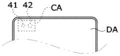
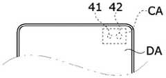
参照图1,可包括显示面板100和外壳,显示面板100的整个表面可形成为显示区域。因而,可实现全屏显示(Full-screen display)。Referring to FIG. 1 , a
显示区域可包括第一显示区域DA和第二显示区域CA。第一显示区域DA和第二显示区域CA都可输出图像,但是分辨率可不同。作为示例,设置在第二显示区域CA中的多个第二像素的分辨率可低于设置在第一显示区域DA中的多个第一像素的分辨率。通过尽量降低设置在第二显示区域CA中的多个第二像素中的分辨率,可向设置在第二显示区域CA中的传感器41和42中注入足够量的光。The display areas may include a first display area DA and a second display area CA. Both the first display area DA and the second display area CA may output images, but resolutions may be different. As an example, the resolution of the plurality of second pixels disposed in the second display area CA may be lower than the resolution of the plurality of first pixels disposed in the first display area DA. A sufficient amount of light can be injected into the
然而,本公开内容不限于此,第一显示区域DA的分辨率和第二显示区域CA的分辨率可相同,只要第二显示区域CA可具有足够的光透射率或者可实现适当的补偿算法即可。However, the present disclosure is not limited thereto, and the resolution of the first display area DA and the resolution of the second display area CA may be the same as long as the second display area CA can have sufficient light transmittance or can implement an appropriate compensation algorithm. Can.
第二显示区域CA可以是设置传感器41和42的区域。第二显示区域CA是与各种传感器重叠的区域,因而可小于输出大部分图像的第一显示区域DA的面积。第二显示区域CA可以是各种传感器收集信息的成像区域。The second display area CA may be an area where the
传感器41和42可包括图像传感器、接近传感器、照度传感器、手势传感器、动作传感器、指纹识别传感器和生物传感器中的至少一种。作为示例,第一传感器41可以是照度传感器或红外传感器,第二传感器42可以是配置为拍摄图像或视频的图像传感器,但本公开内容不必限于此。The
参照图2a至图2d,第二显示区域CA可设置在需要光入射的各种位置。作为示例,第二显示区域CA可如图2a中所示设置在显示区域的左上端,第二显示区域CA可如图2b中所示设置在显示区域的右上端,第二显示区域CA可如图2c中所示设置在显示区域的整个上端,并且第二显示区域CA的宽度可如图2d中所示进行各种修改。然而,本公开内容不必限于此,第二显示区域CA可设置在第一显示区域DA的中央部分或者设置在显示区域的下端。Referring to FIGS. 2a to 2d , the second display area CA may be disposed at various positions where light incidence is required. As an example, the second display area CA can be set at the upper left end of the display area as shown in FIG. 2a, and the second display area CA can be set at the upper right end of the display area as shown in FIG. The setting shown in FIG. 2c is at the entire upper end of the display area, and the width of the second display area CA may be variously modified as shown in FIG. 2d. However, the present disclosure is not necessarily limited thereto, and the second display area CA may be disposed at a central portion of the first display area DA or at a lower end of the display area.
参照图3和图4,第一显示区域DA和第二显示区域CA可包括设置有被写入像素数据的像素的像素阵列。第二显示区域CA的每单位面积的像素数量(下文中称为“每英寸像素数(Pixels Per Inch:PPI)”)可低于第一显示区域DA的PPI,以便确保第二显示区域CA的光透射率。Referring to FIGS. 3 and 4 , the first display area DA and the second display area CA may include pixel arrays provided with pixels to which pixel data is written. The number of pixels per unit area of the second display area CA (hereinafter referred to as "Pixels Per Inch: PPI") may be lower than the PPI of the first display area DA, so as to secure the second display area CA. Light transmittance.
第一显示区域DA的像素阵列可包括设置有具有高PPI的多个像素组的像素区域。第二显示区域CA的像素阵列可包括通过被透光区域间隔开而设置有具有相对低PPI的多个像素组的像素区域。在第二显示区域CA中,外部光可通过具有高光透射率的透光区域穿过显示面板100并且可被放置在显示面板100下方的传感器接收。The pixel array of the first display area DA may include a pixel area provided with a plurality of pixel groups having a high PPI. The pixel array of the second display area CA may include a pixel area provided with a plurality of pixel groups having a relatively low PPI by being spaced apart by a light-transmitting area. In the second display area CA, external light may pass through the
由于第一显示区域DA和第二显示区域CA都包括像素,所以可在第一显示区域DA和第二显示区域CA上再现输入图像。因而,可实现全屏显示(Full-screen display)。Since both the first display area DA and the second display area CA include pixels, an input image may be reproduced on the first display area DA and the second display area CA. Thus, full-screen display can be realized.
第一显示区域DA和第二显示区域CA的每个像素可包括具有不同颜色的子像素,以实现图像的颜色。子像素可包括红色子像素、绿色子像素和蓝色子像素。尽管图中未示出,但像素组可进一步包括白色子像素。每个子像素可包括像素电路部和发光元件(有机发光二极管:OLED)。Each pixel of the first display area DA and the second display area CA may include sub-pixels having different colors to realize colors of images. The sub-pixels may include red sub-pixels, green sub-pixels and blue sub-pixels. Although not shown in the figure, the pixel group may further include white sub-pixels. Each sub-pixel may include a pixel circuit portion and a light emitting element (organic light emitting diode: OLED).
第二显示区域CA可包括像素和设置在显示面板100的屏幕下方的相机模块。相机模块可包括图像传感器。第二显示区域CA的像素可通过在显示模式中写入输入图像的像素数据来显示输入图像。The second display area CA may include pixels and a camera module disposed under the screen of the
相机模块可在成像模式中拍摄外部图像,以输出图片或视频图像数据。相机模块的透镜30可面向第二显示区域CA。外部光通过第二显示区域CA入射到相机模块的透镜30上,并且透镜30可将光会聚到图中省略的图像传感器上。相机模块可在成像模式中拍摄外部图像,以输出图片或视频图像数据。The camera module can capture external images in an imaging mode to output picture or video image data. The
为了确保光透射率,由于从第二显示区域CA去除了像素,所以可应用用于补偿第二显示区域CA中的像素的亮度和色坐标的图像质量补偿算法。In order to ensure light transmittance, since pixels are removed from the second display area CA, an image quality compensation algorithm for compensating brightness and color coordinates of pixels in the second display area CA may be applied.
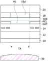
显示面板100可具有沿X轴方向的宽度、沿Y轴方向的长度和沿Z轴方向的厚度。显示面板100可包括设置在基板10上的电路层12、和设置在电路层12上的发光元件层14。可在发光元件层14上设置偏振板18,并且可在偏振板18上设置盖玻璃20。The
电路层12可包括与诸如数据线、栅极线、电源线等之类的线连接的像素电路;与栅极线连接的栅极驱动单元等。The
电路层12可包括电路元件,诸如实现为薄膜晶体管(Thin Film Transistor,TFT)的晶体管、电容器等。电路层12的线和电路元件可由多个绝缘层、之间隔着绝缘层彼此分离的两个或更多个金属层、以及包括半导体材料的有源层实现。The
发光元件层14可包括被像素电路驱动的发光元件。发光元件可实现为OLED。OLED可包括形成在阳极与阴极之间的有机化合物层。The light emitting
有机化合物层可包括空穴注入层(Hole Injection layer,HIL)、空穴传输层(Hole transport layer,HTL)、发光层(Emission layer,EML)、电子传输层(Electrontransport layer,ETL)、和电子注入层(Electron Injection layer,EIL),但本公开内容不限于此。The organic compound layer may include a hole injection layer (Hole Injection layer, HIL), a hole transport layer (Hole transport layer, HTL), an emission layer (Emission layer, EML), an electron transport layer (Electron transport layer, ETL), and electron Injection layer (Electron Injection layer, EIL), but the present disclosure is not limited thereto.
当电压施加至OLED的阳极和阴极时,穿过空穴传输层HTL的空穴和穿过电子传输层ETL的电子移动到发光层EML以产生激子,因而可从发光层EML发射可见光。When a voltage is applied to the anode and cathode of the OLED, holes passing through the hole transport layer HTL and electrons passing through the electron transport layer ETL move to the emission layer EML to generate excitons, and thus visible light can be emitted from the emission layer EML.
发光元件层14可进一步包括设置在像素上的、选择性地透过红色波长、绿色波长和蓝色波长的光的滤色器阵列。The light emitting
发光元件层14可被保护膜覆盖,保护膜可被封装层(encapsulation layer)覆盖。保护膜和封装层可具有其中有机膜和无机膜交替堆叠的结构。无机膜可阻挡湿气或氧气的渗透。有机膜可使无机膜的表面平坦化。当有机膜和无机膜堆叠多层时,由于与单层相比,湿气或氧气的移动路径的长度增加,所以可有效阻挡影响发光元件层14的湿气/氧气的渗透。The light emitting
偏振板18可设置在封装层上。偏振板18可提高显示装置的户外可视性。偏振板18可减小光从显示面板100的表面的反射并且阻挡从电路层12的金属反射的光,从而提高像素的亮度。偏振板18可实现为其中线性偏振板和相位延迟膜结合的偏振板、或者圆偏振板。The
参照图4,第一显示区域DA可包括布置成矩阵形式的多个第一像素组PG1。在多个第一像素组PG1中,两个子像素可使用子像素渲染算法形成一个像素。例如,第一单位像素PIX1可包括R和G1子像素SP1、SP2,第二单位像素PIX2可包括B和G2子像素SP3、SP4。可利用相邻像素之间的各条相应颜色数据的平均值补偿单位像素PIX1和PIX2的每一个中不充分的颜色呈现。然而,本公开内容不必限于此,多个第一像素组PG1可以是包括R子像素、G子像素和B子像素的真实型像素。Referring to FIG. 4 , the first display area DA may include a plurality of first pixel groups PG1 arranged in a matrix form. In the plurality of first pixel groups PG1, two sub-pixels may form one pixel using a sub-pixel rendering algorithm. For example, the first unit pixel PIX1 may include R and G1 sub-pixels SP1, SP2, and the second unit pixel PIX2 may include B and G2 sub-pixels SP3, SP4. Insufficient color representation in each of the unit pixels PIX1 and PIX2 may be compensated for using an average value of respective pieces of corresponding color data between adjacent pixels. However, the present disclosure is not necessarily limited thereto, and the plurality of first pixel groups PG1 may be real-type pixels including R sub-pixels, G sub-pixels, and B sub-pixels.
多个第一像素组PG1的每一个可包括红色发光元件R、第一绿色发光元件G1、蓝色发光元件B和第二绿色发光元件G2。在此,将每个第一像素组PG1中的第一绿色发光元件G1和第二绿色发光元件G2的每一个的中心连接的虚拟线可平行于第一方向。Each of the plurality of first pixel groups PG1 may include a red light emitting element R, a first green light emitting element G1, a blue light emitting element B, and a second green light emitting element G2. Here, a virtual line connecting centers of each of the first green light emitting element G1 and the second green light emitting element G2 in each first pixel group PG1 may be parallel to the first direction.
图5是图解根据本公开内容一个实施方式的第二显示区域的像素和透光区域的视图。FIG. 5 is a view illustrating pixels of a second display area and a light transmission area according to one embodiment of the present disclosure.
参照图5,第二显示区域CA可包括多个第二像素组PG2和多个透光区域TA。多个透光区域TA可设置在多个第二像素组PG2之间。具体地,透光区域TA与第二像素组PG2可沿第一方向和第二方向交替设置。外部光可通过透光区域TA被接收到相机模块的透镜。第二显示区域CA的分辨率可相对于第一显示区域DA的分辨率降低透光区域TA的面积增加的程度。Referring to FIG. 5 , the second display area CA may include a plurality of second pixel groups PG2 and a plurality of light transmitting areas TA. A plurality of light transmitting areas TA may be disposed between the plurality of second pixel groups PG2. Specifically, the light-transmitting area TA and the second pixel group PG2 may be alternately arranged along the first direction and the second direction. External light may be received to the lens of the camera module through the light transmission area TA. The resolution of the second display area CA may be reduced relative to the resolution of the first display area DA by an increase in the area of the light-transmitting area TA.
透光区域TA可包括具有高光透射率而不具有金属的透明介质,使得光可以以最小的光损耗进行入射。透光区域TA可由不包括金属线或像素的透明绝缘材料制成。随着透光区域TA变得更大,第二显示区域CA的光透射率可更高。The light transmission area TA may include a transparent medium having high light transmittance without metal so that light may be incident with minimal light loss. The light transmitting area TA may be made of a transparent insulating material that does not include metal lines or pixels. As the light transmission area TA becomes larger, the light transmittance of the second display area CA may be higher.
多个第二像素组PG2的每一个可包括一个或两个像素。例如,在每个第二像素组PG2中,第一单位像素PIX1可包括R和G1子像素SP1、SP2,第二单位像素PIX2可包括B和G2子像素SP3、SP4。第二像素组PG2的像素的形状和布置可与第一像素组PG1的像素的形状和布置相同或不同。Each of the plurality of second pixel groups PG2 may include one or two pixels. For example, in each second pixel group PG2, the first unit pixel PIX1 may include R and G1 sub-pixels SP1, SP2, and the second unit pixel PIX2 may include B and G2 sub-pixels SP3, SP4. The shape and arrangement of pixels of the second pixel group PG2 may be the same as or different from those of the first pixel group PG1.
透光区域TA的形状被示出为是四边形形状,但本公开内容不限于此。例如,透光区域TA可设计为各种形状,诸如圆形形状、椭圆形形状、多边形形状等。The shape of the light transmitting area TA is shown as a quadrangular shape, but the present disclosure is not limited thereto. For example, the light-transmitting area TA may be designed in various shapes, such as a circular shape, an elliptical shape, a polygonal shape, and the like.
可从透光区域TA去除全部金属电极材料。因此,像素的各线TS可设置在透光区域TA外部。因此,光可通过透光区域有效地入射。然而,本公开内容不必限于此,在透光区域TA的部分区域中可存在金属电极材料。All metal electrode material may be removed from the light transmissive area TA. Accordingly, each line TS of a pixel may be disposed outside the light transmission area TA. Therefore, light can be efficiently incident through the light-transmitting region. However, the present disclosure is not necessarily limited thereto, and a metal electrode material may exist in a partial area of the light transmission area TA.
图6是图解第二显示区域的显示面板的结构的示意图,图7是图6的修改例。FIG. 6 is a schematic diagram illustrating a structure of a display panel of a second display area, and FIG. 7 is a modified example of FIG. 6 .
参照图6,显示面板可包括设置在基板10上的电路层12、和设置在电路层12上的发光元件层14。可在发光元件层14上设置偏振板18,并且可在偏振板18上设置盖玻璃20。Referring to FIG. 6 , the display panel may include a
在偏振板18中,可在与透光区域TA对应的区域中形成第一透光图案18d。基于具有555nm波长的绿色光,由PI制成的基板的光透射率大约为70%至80%,并且阴极的光透射率为80%至90%。另一方面,偏振板18的光透射率相对非常低,大约为40%。因而,为了有效增加透光区域中的光透射率,需要增加偏振板18的光透射率。In the
根据该实施方式的偏振板18具有形成在透光区域TA上的第一透光图案18d,以增加光透射率。在偏振板中形成有第一透光图案的区域的光透射率可最高。因而,在透光区域中进入相机模块中的光量增加,从而提高相机性能。The
偏振板18的第一透光图案18d可通过去除偏振板18的一部分来形成,也可通过分解构成偏振板18的化合物来形成。就是说,第一透光图案18d可具有能够增加常规偏振板18的光透射率的各种结构。The first light-transmitting
参照图7,在透光区域TA中,偏振板18可具有第一透光图案18d,并且阴极CAT可具有第二透光图案。第二透光图案可以是形成在透光区域TA中的开口H1。由于阴极的光透射率为80%至90%,所以透光区域TA的光透射率可由于开口H1而进一步增加。Referring to FIG. 7 , in the light transmission area TA, the
在阴极CAT中形成开口H1的方法没有特别限制。作为示例,在形成阴极之后,可使用蚀刻工艺在阴极中形成开口H1,或者可使用在基板10的下部的红外(IR)激光器去除阴极。A method of forming the opening H1 in the cathode CAT is not particularly limited. As an example, after the cathode is formed, the opening H1 may be formed in the cathode using an etching process, or the cathode may be removed using an infrared (IR) laser at a lower portion of the
可在阴极CAT上形成偏振层PCL,并且可在偏振层PCL上设置触摸传感器TOE。在此,在透光区域TA中,触摸传感器的感测电极和线可由诸如氧化铟锡(ITO)之类的透明材料或金属网制成,从而增加光透射率。A polarizing layer PCL may be formed on the cathode CAT, and a touch sensor TOE may be disposed on the polarizing layer PCL. Here, in the light transmission area TA, the sensing electrodes and lines of the touch sensor may be made of a transparent material such as indium tin oxide (ITO) or a metal mesh, thereby increasing light transmittance.
图8是图解根据本公开内容第一实施方式的第二显示区域中的像素布置的视图,图9是图8的局部放大图。FIG. 8 is a view illustrating a pixel arrangement in a second display area according to the first embodiment of the present disclosure, and FIG. 9 is a partially enlarged view of FIG. 8 .
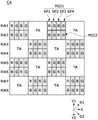
参照图8和图9,第二显示区域CA可包括多个第二像素组PG2和多个透光区域TA。多个第二像素组PG2可沿第一方向和第二方向设置在多个像素行RW1至RW8和多个像素列中。下文中,第一方向可以是X轴方向,第二方向可以是Y1轴或Y2轴方向。在此,像素行和像素列可指设置多个子像素的行和列,透光区域可设置在行和列的部分区域或全部区域中。Referring to FIGS. 8 and 9 , the second display area CA may include a plurality of second pixel groups PG2 and a plurality of light transmitting areas TA. A plurality of second pixel groups PG2 may be disposed in a plurality of pixel rows RW1 to RW8 and a plurality of pixel columns along the first direction and the second direction. Hereinafter, the first direction may be the X-axis direction, and the second direction may be the Y1-axis or Y2-axis direction. Here, pixel rows and pixel columns may refer to rows and columns in which a plurality of sub-pixels are arranged, and the light-transmitting regions may be arranged in part or all of the rows and columns.
每个第二像素组PG2可包括第一子像素SP1、第二子像素SP2和第三子像素SP3。第一子像素SP1可包括第一发光元件R,第二子像素SP2可包括第二发光元件G1,第三子像素SP3可包括第三发光元件B。Each second pixel group PG2 may include a first subpixel SP1, a second subpixel SP2, and a third subpixel SP3. The first subpixel SP1 may include a first light emitting element R, the second subpixel SP2 may include a second light emitting element G1, and the third subpixel SP3 may include a third light emitting element B.
第一发光元件R可以是红色发光元件,第二发光元件G1可以是绿色发光元件,第三发光元件B可以是蓝色发光元件,但本公开内容不必限于此,发光波长可进行各种修改。The first light emitting element R may be a red light emitting element, the second light emitting element G1 may be a green light emitting element, and the third light emitting element B may be a blue light emitting element, but the present disclosure is not necessarily limited thereto, and the light emission wavelength may be variously modified.
根据该实施方式,第一至第三子像素SP1至SP3可实现为构成一个像素的真实型像素,但本公开内容不必限于此。作为示例,第二像素组PG2可进一步包括第四子像素,第四子像素可包括绿色发光元件或白色发光元件。每个发光元件可以是有机或无机发光元件。According to this embodiment, the first to third sub-pixels SP1 to SP3 may be implemented as true type pixels constituting one pixel, but the present disclosure is not necessarily limited thereto. As an example, the second pixel group PG2 may further include a fourth sub-pixel, and the fourth sub-pixel may include a green light emitting element or a white light emitting element. Each light emitting element may be an organic or inorganic light emitting element.
多个子像素SP1、SP2和SP3可沿第一方向或第二方向具有规则的布置。第一子像素SP1、第二子像素SP2和第三子像素SP3可沿第一方向顺序地设置。The plurality of sub-pixels SP1, SP2, and SP3 may have a regular arrangement along the first or second direction. The first subpixel SP1, the second subpixel SP2, and the third subpixel SP3 may be sequentially disposed along the first direction.
透光区域TA的宽度可对应于每个子像素的宽度。根据这种结构,可以以相对较小的结构设置大量的透光区域TA,使得可确保均匀的透光区域。然而,本公开内容不必限于此,透光区域的尺寸可进行各种调整。此外,尽管透光区域被示出为具有四边形形状,但也可应用圆形或多边形形状。The width of the light transmission area TA may correspond to the width of each sub-pixel. According to this structure, a large number of light-transmitting areas TA can be provided with a relatively small structure, so that uniform light-transmitting areas can be ensured. However, the present disclosure is not necessarily limited thereto, and the size of the light-transmitting region may be variously adjusted. Furthermore, although the light transmissive area is shown as having a quadrangular shape, a circular or polygonal shape may also be applied.
第一发光元件R与第三发光元件B可沿第一方向和第二方向交替设置。第二发光元件G1可在第一方向和第二方向上不与第一发光元件R和第三发光元件B重叠。The first light emitting elements R and the third light emitting elements B may be arranged alternately along the first direction and the second direction. The second light emitting element G1 may not overlap the first light emitting element R and the third light emitting element B in the first direction and the second direction.
第二发光元件G1与第三发光元件B可沿第一斜线方向D1交替设置,并且第二发光元件G1与第一发光元件R可沿第二斜线方向D2交替设置。第一斜线方向D1可以是Y1轴与X轴之间的斜线方向,第二斜线方向D2可以是Y2轴与X轴之间的斜线方向。The second light emitting elements G1 and the third light emitting elements B may be alternately arranged along the first oblique direction D1, and the second light emitting elements G1 and the first light emitting elements R may be alternately arranged along the second oblique direction D2. The first oblique direction D1 may be an oblique direction between the Y1 axis and the X axis, and the second oblique direction D2 may be an oblique direction between the Y2 axis and the X axis.
多个第二像素组PG2的第一发光元件R可设置在倾斜45°的第一方形线P1上。此外,第二发光元件G1可设置在第二方形线P2上,并且第三发光元件B可设置在第三方形线P3上。就是说,每个发光元件可设置为其中相同颜色的发光元件以四边形形状设置的结构。The first light emitting elements R of the plurality of second pixel groups PG2 may be disposed on the first square line P1 inclined at 45°. In addition, the second light emitting element G1 may be disposed on the second square line P2, and the third light emitting element B may be disposed on the third square line P3. That is, each light emitting element may be arranged in a structure in which light emitting elements of the same color are arranged in a quadrangular shape.
根据该实施方式,由于每个发光元件的中心(或每个子像素的中心)设置在方形线上,所以各个发光元件之间的距离变得均匀,使得具有甚至当省略一些像素时仍可实现相对均匀的图像质量的优点。此外,从外部不会观察到像素图案,使得可提高图像质量。According to this embodiment, since the center of each light-emitting element (or the center of each sub-pixel) is arranged on a square line, the distance between the respective light-emitting elements becomes uniform, making it possible to achieve a relative pixel even when some pixels are omitted. The advantage of uniform image quality. In addition, pixel patterns are not observed from the outside, so that image quality can be improved.
参照图9,在子像素SP1、SP2和SP3中可分别设置有电路部CT1、CT2和CT3。电路部CT1、CT2和CT3可各自包括与线TS连接的像素电路,以驱动像素。Referring to FIG. 9 , circuit parts CT1 , CT2 and CT3 may be disposed in the sub-pixels SP1 , SP2 and SP3 , respectively. The circuit parts CT1, CT2, and CT3 may each include a pixel circuit connected to the line TS to drive the pixel.
线TS可设置为绕过透光区域TA。在此,术语“绕过”可指线TS设置为尽可能少地覆盖透光区域TA。就是说,线可设置在部分透光区域中。此外,阴极的与透光区域TA对应的部分可被图案化,以增加光透射率。The line TS may be disposed to bypass the light-transmitting area TA. Here, the term "bypass" may mean that the wire TS is arranged to cover the light-transmitting area TA as little as possible. That is, the wires may be provided in partially light-transmitting regions. In addition, a portion of the cathode corresponding to the light transmission area TA may be patterned to increase light transmittance.
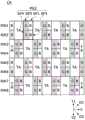
图10是图解根据本公开内容第二实施方式的第二显示区域中的像素布置的视图。图11a是图10的局部放大图。图11b是图11a的修改例。FIG. 10 is a view illustrating a pixel arrangement in a second display area according to a second embodiment of the present disclosure. FIG. 11 a is a partially enlarged view of FIG. 10 . Fig. 11b is a modified example of Fig. 11a.
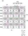
参照图10和图11a,第二显示区域CA可包括多个第二像素组PG2和多个透光区域TA。每个第二像素组PG2可包括具有不同子像素布置的第2-1像素组PG21和第2-2像素组PG22。每个第二像素组PG2可包括第一子像素SP1、第二子像素SP2、第三子像素SP3和第四子像素SP4。Referring to FIGS. 10 and 11a, the second display area CA may include a plurality of second pixel groups PG2 and a plurality of light-transmitting areas TA. Each second pixel group PG2 may include a 2-1 pixel group PG21 and a 2-2 pixel group PG22 having different sub-pixel arrangements. Each second pixel group PG2 may include a first subpixel SP1, a second subpixel SP2, a third subpixel SP3, and a fourth subpixel SP4.
第一子像素SP1可包括第一发光元件R,第二子像素SP2可包括第二发光元件G1,第三子像素SP3可包括第三发光元件B,第四子像素SP4可包括第四发光元件G2。The first sub-pixel SP1 may include a first light-emitting element R, the second sub-pixel SP2 may include a second light-emitting element G1, the third sub-pixel SP3 may include a third light-emitting element B, and the fourth sub-pixel SP4 may include a fourth light-emitting element. G2.
第一发光元件R可以是红色发光元件,第二发光元件G1和第四发光元件G2可以是绿色发光元件,第三发光元件B可以是蓝色发光元件,但本公开内容不必限于此,每个发光元件的发光波长可进行各种修改。The first light-emitting element R may be a red light-emitting element, the second light-emitting element G1 and the fourth light-emitting element G2 may be green light-emitting elements, and the third light-emitting element B may be a blue light-emitting element, but the present disclosure is not necessarily limited thereto, each The emission wavelength of the light emitting element can be variously modified.
第四子像素SP4可设置在与第一至第三子像素SP1至SP3不同的像素行中。作为示例,在第2-1像素组PG21中,第一至第三子像素SP1至SP3可设置在第一像素行RW1中,而第四子像素SP4可设置在第二像素行RW2中。第二子像素SP2的第二发光元件G1和第四子像素SP4的第四发光元件G2可沿第二斜线方向D2设置。The fourth sub-pixel SP4 may be disposed in a different pixel row from the first to third sub-pixels SP1 to SP3. As an example, in the 2-1 pixel group PG21, the first to third sub-pixels SP1 to SP3 may be disposed in the first pixel row RW1, and the fourth sub-pixel SP4 may be disposed in the second pixel row RW2. The second light emitting element G1 of the second subpixel SP2 and the fourth light emitting element G2 of the fourth subpixel SP4 may be disposed along the second oblique direction D2.
然而,本公开内容不必限于此,第四子像素SP4的电路部可形成在第一像素行RW1中并且第四发光元件G2的一部分可设置在第二像素行RW2中。就是说,表述“一个子像素设置在与其他子像素不同的像素行中”的含义可包括其中电路部和发光元件都设置在不同像素行中的情况、以及其中电路部和发光元件的至少一部分设置在不同像素行中的情况。However, the present disclosure is not necessarily limited thereto, and the circuit part of the fourth subpixel SP4 may be formed in the first pixel row RW1 and a part of the fourth light emitting element G2 may be provided in the second pixel row RW2. That is, the meaning of the expression "one sub-pixel is provided in a pixel row different from other sub-pixels" may include the case where both the circuit section and the light-emitting element are provided in a different pixel row, and the case where at least a part of the circuit section and the light-emitting element Cases set in different pixel rows.
相比之下,在第2-2像素组PG22中,第一子像素SP1、第三子像素SP3和第四子像素SP4可设置在第二像素行RW2中,而第二子像素SP2可设置在第一像素行RW1中。就是说,相邻的第2-1像素组PG21和第2-2像素组PG22可具有不同的像素布置。根据这种配置,第2-2像素组PG22的第二子像素SP2可设置于在第一方向上相邻的第2-1像素组PG21之间的透光区域TA中,从而提高均匀性和亮度。In contrast, in the 2-2 pixel group PG22, the first sub-pixel SP1, the third sub-pixel SP3, and the fourth sub-pixel SP4 may be disposed in the second pixel row RW2, and the second sub-pixel SP2 may be disposed In the first pixel row RW1. That is, adjacent 2-1 pixel groups PG21 and 2-2 pixel groups PG22 may have different pixel arrangements. According to this configuration, the second sub-pixel SP2 of the 2-2th pixel group PG22 can be disposed in the light-transmitting area TA between the 2-1st pixel group PG21 adjacent in the first direction, thereby improving uniformity and brightness.
第一发光元件R与第三发光元件B可沿第一方向交替设置。第二发光元件G1可在第一方向上不与第一发光元件R和第三发光元件B重叠。此外,第一发光元件R、第二发光元件G1和第三发光元件B可设置为在第二方向上彼此不重叠。The first light emitting elements R and the third light emitting elements B may be arranged alternately along the first direction. The second light emitting element G1 may not overlap the first light emitting element R and the third light emitting element B in the first direction. In addition, the first light emitting element R, the second light emitting element G1 and the third light emitting element B may be disposed not to overlap each other in the second direction.
第二发光元件G1或第四发光元件G2与第三发光元件B可沿第一斜线方向D1交替设置,并且第一发光元件R可在第一斜线方向D1上不与第二发光元件G1、第四发光元件G2和第三发光元件B重叠。The second light-emitting element G1 or the fourth light-emitting element G2 and the third light-emitting element B can be arranged alternately along the first oblique direction D1, and the first light-emitting element R can be separated from the second light-emitting element G1 in the first oblique direction D1. , the fourth light emitting element G2 and the third light emitting element B overlap.
第一发光元件R与第二发光元件G1和第四发光元件G2可沿第二斜线方向D2交替设置,并且第三发光元件B可在第二斜线方向D2上不与第一发光元件R、第二发光元件G1和第四发光元件G2重叠。The first light-emitting element R, the second light-emitting element G1 and the fourth light-emitting element G2 may be arranged alternately along the second oblique direction D2, and the third light-emitting element B may not be separated from the first light-emitting element R in the second oblique direction D2. , the second light emitting element G1 and the fourth light emitting element G2 overlap.
根据该布置,由于第二子像素SP2和第四子像素SP4可沿斜线方向均匀设置,所以与第一显示区域DA相比具有即使当省略一些像素时仍可实现均匀的图像质量的优点。此外,从外部不会观察到像素图案,使得可提高图像质量。According to this arrangement, since the second subpixel SP2 and the fourth subpixel SP4 can be uniformly arranged in the oblique direction, there is an advantage that uniform image quality can be achieved even when some pixels are omitted, compared to the first display area DA. In addition, pixel patterns are not observed from the outside, so that image quality can be improved.
尽管举例说明了可形成各种尺寸的多个透光区域TA的情况,但每个透光区域TA的尺寸可相同。作为示例,每个透光区域TA可具有与子像素的尺寸对应的尺寸。Although the case where a plurality of light transmitting areas TA may be formed in various sizes is exemplified, the size of each light transmitting area TA may be the same. As an example, each light transmitting area TA may have a size corresponding to the size of a sub-pixel.
参照图11b,透光区域TA可设置在构成第二像素组PG2的第三子像素SP3和第四子像素SP4之间。在第二像素组PG2之间的透光区域TA较大的情况下,存在相应的透光区域TA的亮度相对降低,使得图像质量劣化的问题,但是根据该实施方式,第四子像素SP4可设置在透光区域TA之间,使得可提高均匀性和亮度。Referring to FIG. 11b, the light transmitting area TA may be disposed between the third sub-pixel SP3 and the fourth sub-pixel SP4 constituting the second pixel group PG2. In the case where the light-transmitting area TA between the second pixel group PG2 is relatively large, there is a problem that the brightness of the corresponding light-transmitting area TA is relatively reduced, which degrades the image quality. However, according to this embodiment, the fourth sub-pixel SP4 can Disposed between the light-transmitting areas TA, so that uniformity and brightness can be improved.
作为示例,在第2-1像素组PG21中透光区域TA可设置在第三子像素SP3和第四子像素SP4之间,而在第2-2像素组PG22中透光区域TA可设置在第二子像素SP2和第三子像素SP3之间。此外,设置在第2-1像素组PG21中的透光区域TA的尺寸和设置在第2-2像素组PG22中的透光区域TA的尺寸可不同。As an example, in the 2-1 pixel group PG21, the light-transmitting area TA may be disposed between the third sub-pixel SP3 and the fourth sub-pixel SP4, and in the 2-2 pixel group PG22, the light-transmitting area TA may be disposed between Between the second sub-pixel SP2 and the third sub-pixel SP3. In addition, the size of the light-transmitting area TA disposed in the 2-1 pixel group PG21 and the size of the light-transmitting area TA disposed in the 2-2 pixel group PG22 may be different.
根据一实施方式,将多个子像素分组以形成像素组的方法可进行各种修改。图12是图解根据本公开内容第三实施方式的第二显示区域中的像素布置的视图。According to an embodiment, a method of grouping a plurality of sub-pixels to form a pixel group may be variously modified. FIG. 12 is a view illustrating a pixel arrangement in a second display area according to a third embodiment of the present disclosure.
参照图12,第一子像素SP1和第三子像素SP3可设置在第一像素行RW1中,而第二子像素SP2和第四子像素SP4可设置在第二像素行RW2中。Referring to FIG. 12 , the first and third subpixels SP1 and SP3 may be disposed in a first pixel row RW1 , and the second and fourth subpixels SP2 and SP4 may be disposed in a second pixel row RW2 .
因此,可在第一像素行RW1中交替设置第一发光元件R和第三发光元件B,并且可在第二像素行RW2中交替设置第二发光元件G1和第四发光元件G2。Accordingly, the first light emitting element R and the third light emitting element B may be alternately arranged in the first pixel row RW1, and the second light emitting element G1 and the fourth light emitting element G2 may be alternately arranged in the second pixel row RW2.
然而,本公开内容不必限于此,第二子像素SP2和第四子像素SP4的每一个的电路部可形成在第一像素行RW1中,并且第二发光元件G1和第四发光元件G2的每一个的一部分可设置在第二像素行RW2中。However, the present disclosure is not necessarily limited thereto, a circuit portion of each of the second subpixel SP2 and the fourth subpixel SP4 may be formed in the first pixel row RW1, and each of the second light emitting element G1 and the fourth light emitting element G2 A portion of one may be disposed in the second pixel row RW2.
此外,第二子像素SP2的第二发光元件G1和第四子像素SP4的第四发光元件G2可具有不同的形状。作为示例,第二发光元件G1可具有沿第二斜线方向D2延伸的形状,而第四发光元件G2可具有沿第一斜线方向D1延伸的形状。In addition, the second light emitting element G1 of the second subpixel SP2 and the fourth light emitting element G2 of the fourth subpixel SP4 may have different shapes. As an example, the second light emitting element G1 may have a shape extending in the second oblique direction D2, and the fourth light emitting element G2 may have a shape extending in the first oblique direction D1.
第二像素行RW2中的第二发光元件G1和第四像素行RW4中的第二发光元件G1也可被制造为具有不同的形状。就是说,第二发光元件G1可被制造为在第二方向上具有不同的形状。类似地,第二像素行RW2的第四发光元件G2和第四像素行RW4的第四发光元件G2可被制造为在第二方向上具有不同的形状。The second light emitting element G1 in the second pixel row RW2 and the second light emitting element G1 in the fourth pixel row RW4 may also be manufactured to have different shapes. That is, the second light emitting element G1 may be manufactured to have different shapes in the second direction. Similarly, the fourth light emitting element G2 of the second pixel row RW2 and the fourth light emitting element G2 of the fourth pixel row RW4 may be manufactured to have different shapes in the second direction.
由于发光元件以这种方式进行各种修改,所以当在基板上形成有机发光元件时,所以可不同地制造用于第一显示区域的精细金属掩模(Fine Metal Mask,FMM)和用于第二显示区域CA的FMM。Since the light emitting element is variously modified in this way, when the organic light emitting element is formed on the substrate, a Fine Metal Mask (FMM) for the first display area and a fine metal mask (FMM) for the second display area can be manufactured differently. 2 shows the FMM of the region CA.
作为示例,在用于第一显示区域的FMM中,可在第二发光元件G1和第四发光元件G2中形成具有相同形状的开口,而在用于第二显示区域的FMM中,可通过改变发光元件的形状和布置来形成开口,以有利于提高图像质量。因而,第一显示区域DA中的像素的形状和/或布置可与第二显示区域CA中的像素的形状和/或布置不同。As an example, in the FMM used for the first display area, openings having the same shape can be formed in the second light emitting element G1 and the fourth light emitting element G2, and in the FMM used for the second display area, openings can be formed by changing The shape and arrangement of the light emitting elements to form openings are beneficial to improve image quality. Thus, the shape and/or arrangement of pixels in the first display area DA may be different from the shape and/or arrangement of pixels in the second display area CA.
根据该实施方式,可通过不同地形成第一显示区域DA的发光元件和第二显示区域CA的发光元件的形状和/或布置提高均匀性和亮度。根据一实施方式,将多个子像素分组以形成像素组的方法可进行各种修改。According to this embodiment, uniformity and brightness may be improved by differently forming the shape and/or arrangement of the light emitting elements of the first display area DA and the light emitting elements of the second display area CA. According to an embodiment, a method of grouping a plurality of sub-pixels to form a pixel group may be variously modified.
图13是图解第二显示区域中的像素布置的第一比较例。图14图解了从外部是否识别到图案的观察结果。图15是图解第二显示区域中的像素布置的第二比较例。FIG. 13 is a first comparative example illustrating the arrangement of pixels in the second display area. FIG. 14 illustrates observation results of whether a pattern is recognized from the outside. FIG. 15 is a second comparative example illustrating the arrangement of pixels in the second display area.
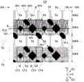
参照图13,可在第一像素行RW1和第四像素行RW4的每一个中设置红色发光元件和蓝色发光元件,并且可在第二像素行RW2中设置绿色发光元件。在这种情况下,也可在第三像素行RW3中设置绿色发光元件。Referring to FIG. 13 , a red light emitting element and a blue light emitting element may be disposed in each of the first and fourth pixel rows RW1 and RW4 , and a green light emitting element may be disposed in the second pixel row RW2 . In this case, green light emitting elements may also be provided in the third pixel row RW3.
因此,由于在第二像素行RW2和第三像素行RW3中仅设置绿色发光元件,所以存在亮度均匀性相对降低的问题。结果,如图14中所示,从外部观察到线形图案Q1,因而存在图像质量劣化的问题。Therefore, since only green light emitting elements are disposed in the second pixel row RW2 and the third pixel row RW3 , there is a problem that brightness uniformity is relatively lowered. As a result, as shown in FIG. 14 , the linear pattern Q1 is observed from the outside, and thus there is a problem of image quality degradation.
参照图15,在第二像素行RW2和第三像素行RW3中仅设置绿色发光元件,因而存在从外部识别到线形图案的问题。相比之下,在本公开内容实施方式的情况下,由于子像素相对均匀地设置,所以具有提高图像质量的效果。Referring to FIG. 15 , only green light emitting elements are disposed in the second pixel row RW2 and the third pixel row RW3 , and thus there is a problem of recognizing the line pattern from the outside. In contrast, in the case of the embodiment of the present disclosure, since the sub-pixels are arranged relatively uniformly, there is an effect of improving image quality.
图16是图解根据本公开内容第四实施方式的第二显示区域中的像素布置的视图。图17是图解根据本公开内容第五实施方式的第二显示区域中的像素布置的视图。FIG. 16 is a view illustrating a pixel arrangement in a second display area according to a fourth embodiment of the present disclosure. FIG. 17 is a view illustrating a pixel arrangement in a second display area according to a fifth embodiment of the present disclosure.
参照图16,在第二像素组PG2中,第一子像素SP1和第二子像素SP2可设置在第一像素行RW1中,并且第三子像素SP3和第四子像素SP4可设置在第二像素行RW2中。16, in the second pixel group PG2, the first subpixel SP1 and the second subpixel SP2 may be disposed in the first pixel row RW1, and the third subpixel SP3 and the fourth subpixel SP4 may be disposed in the second pixel row RW1. pixel row RW2.
此外,第二子像素SP2和第三子像素SP3可沿第二斜线方向D2设置,并且第一子像素SP1和第三子像素SP3可沿第一斜线方向D1设置。透光区域TA可设置在多个第二像素组PG2之间。透光区域TA也可形成为对应于第二像素组PG2的尺寸。In addition, the second subpixel SP2 and the third subpixel SP3 may be disposed along the second oblique direction D2, and the first subpixel SP1 and the third subpixel SP3 may be disposed along the first oblique direction D1. The light transmitting area TA may be disposed between the plurality of second pixel groups PG2. The light transmitting area TA may also be formed to correspond to the size of the second pixel group PG2.
参照图17,在第二像素组PG2中,第一子像素SP1和第二子像素SP2可设置在第一像素行RW1中,并且第三子像素SP3和第四子像素SP4可设置在第二像素行RW2中。17, in the second pixel group PG2, the first subpixel SP1 and the second subpixel SP2 may be disposed in the first pixel row RW1, and the third subpixel SP3 and the fourth subpixel SP4 may be disposed in the second pixel row RW1. pixel row RW2.
此外,第一子像素SP1和第四子像素SP4可沿第二斜线方向D2设置,并且第二子像素SP2和第三子像素SP3可沿第一斜线方向D1设置。透光区域TA可设置在多个第二像素组PG2之间。透光区域TA也可形成为对应于第二像素组PG2的尺寸。In addition, the first subpixel SP1 and the fourth subpixel SP4 may be disposed along the second oblique direction D2, and the second subpixel SP2 and the third subpixel SP3 may be disposed along the first oblique direction D1. The light transmitting area TA may be disposed between the plurality of second pixel groups PG2. The light transmitting area TA may also be formed to correspond to the size of the second pixel group PG2.
图18是图解根据本公开内容第六实施方式的第二显示区域中的像素布置的视图。图19是图解根据本公开内容第七实施方式的第二显示区域中的像素布置的视图。FIG. 18 is a view illustrating a pixel arrangement in a second display area according to a sixth embodiment of the present disclosure. FIG. 19 is a view illustrating a pixel arrangement in a second display area according to a seventh embodiment of the present disclosure.
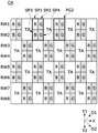
参照图18,在第二像素组PG2中,第一至第四子像素SP1、SP2、SP3和SP4可设置在同一像素行中。第二像素组PG2与透光区域TA可沿第一方向和第二方向交替设置。在此,透光区域TA的尺寸可对应于第二像素组PG2的尺寸。Referring to FIG. 18 , in the second pixel group PG2 , first to fourth subpixels SP1 , SP2 , SP3 and SP4 may be disposed in the same pixel row. The second pixel group PG2 and the transparent area TA may be alternately arranged along the first direction and the second direction. Here, the size of the light transmission area TA may correspond to the size of the second pixel group PG2.
参照图19,第二像素组PG2包括第一至第四子像素SP1、SP2、SP3和SP4,并且第二像素组PG2与透光区域TA可沿第一方向交替设置。在第二方向上,第2-1像素组PG21与第2-2像素组PG22可交替设置。在第2-1像素组PG21和第2-2像素组PG22中,第一子像素SP1和第三子像素SP3的位置可彼此不同。Referring to FIG. 19 , the second pixel group PG2 includes first to fourth sub-pixels SP1 , SP2 , SP3 and SP4 , and the second pixel group PG2 and the light transmission area TA may be alternately arranged along the first direction. In the second direction, the 2-1 pixel group PG21 and the 2-2 pixel group PG22 may be arranged alternately. In the 2-1 pixel group PG21 and the 2-2 pixel group PG22, the positions of the first sub-pixel SP1 and the third sub-pixel SP3 may be different from each other.
图20是图解根据本公开内容第八实施方式的第二显示区域中的像素布置的视图,图21是图20的放大图,图22是图21的一修改例,图23是图21的第二修改例。20 is a view illustrating a pixel arrangement in a second display area according to an eighth embodiment of the present disclosure, FIG. 21 is an enlarged view of FIG. 20 , FIG. 22 is a modified example of FIG. 21 , and FIG. Two modified examples.
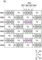
参照图20,在第二像素组PG2中,第一子像素SP1、第二子像素SP2和第三子像素SP3可沿第一方向设置,并且第四子像素SP4可沿第三子像素SP3的第二斜线方向D2设置。Referring to FIG. 20 , in the second pixel group PG2, the first subpixel SP1, the second subpixel SP2, and the third subpixel SP3 may be arranged along the first direction, and the fourth subpixel SP4 may be arranged along the direction of the third subpixel SP3. The second oblique direction D2 is set.
透光区域TA可设置在多个第二像素组PG2之间。在这种情况下,透光区域TA可包括与每个子像素的宽度对应的区域和与三个子像素的宽度对应的区域。就是说,多个透光区域TA的尺寸可彼此不同。然而,本公开内容不必限于此,多个透光区域TA的尺寸也可相同。The light transmitting area TA may be disposed between the plurality of second pixel groups PG2. In this case, the light transmitting area TA may include an area corresponding to the width of each sub-pixel and an area corresponding to the width of three sub-pixels. That is, the sizes of the plurality of transmissive areas TA may be different from each other. However, the present disclosure is not necessarily limited thereto, and the sizes of the plurality of light-transmitting areas TA may also be the same.
第一至第三子像素SP1、SP2和SP3可沿第一方向交替设置。第四子像素SP4可在第一方向上不与第一至第三子像素SP1、SP2和SP3重叠。第一至第四子像素SP1、SP2、SP3和SP4可设置为在第二方向上彼此不重叠。The first to third sub-pixels SP1, SP2 and SP3 may be alternately arranged along the first direction. The fourth subpixel SP4 may not overlap the first to third subpixels SP1, SP2, and SP3 in the first direction. The first to fourth sub-pixels SP1, SP2, SP3, and SP4 may be disposed not to overlap each other in the second direction.
多个第二像素组PG2的第一至第四子像素SP1、SP2、SP3和SP4可设置在方形线P1、P2、P3和P4的每一个上。此外,第一至第三子像素SP1、SP2和SP3可设置在将第四子像素SP4连接的方形线P4内部。根据该布置,由于所有子像素均匀地设置,所以即使当与第一显示区域DA相比省略了一些像素,也可实现均匀的图像质量。此外,不会从外部观察到像素图案,使得可提高图像质量。The first to fourth sub-pixels SP1, SP2, SP3 and SP4 of the plurality of second pixel groups PG2 may be disposed on each of the square lines P1, P2, P3 and P4. In addition, the first to third subpixels SP1, SP2, and SP3 may be disposed inside a square line P4 connecting the fourth subpixel SP4. According to this arrangement, even when some pixels are omitted compared with the first display area DA, uniform image quality can be achieved since all sub-pixels are uniformly arranged. In addition, pixel patterns are not observed from the outside, so that image quality can be improved.
在该实施方式中,描述了第四子像素SP4设置在与第一至第三子像素SP1至SP3不同的像素行中,但本公开内容不必限于此。第四子像素SP4的电路部可形成在第一像素行RW1中,并且第四发光元件的一部分可设置在第二像素行RW2中。In this embodiment, it is described that the fourth sub-pixel SP4 is disposed in a different pixel row from the first to third sub-pixels SP1 to SP3, but the present disclosure is not necessarily limited thereto. A circuit part of the fourth subpixel SP4 may be formed in the first pixel row RW1, and a part of the fourth light emitting element may be disposed in the second pixel row RW2.
参照图21,第二显示区域CA可包括其中多个第二像素组PG2沿第一方向连续设置的奇数像素行RW3和RW5、以及其中多个透光区域TA沿第一方向连续设置的偶数像素行RW2和RW4,奇数像素行RW3和RW5与偶数像素行RW2和RW4可沿第二方向交替设置。Referring to FIG. 21 , the second display area CA may include odd-numbered pixel rows RW3 and RW5 in which a plurality of second pixel groups PG2 are continuously arranged along the first direction, and even-numbered pixels in which a plurality of light-transmitting areas TA are continuously arranged along the first direction. The rows RW2 and RW4, the odd pixel rows RW3 and RW5 and the even pixel rows RW2 and RW4 may be alternately arranged along the second direction.
设置在奇数像素行RW3和RW5的每一个中的子像素SP1、SP2、SP3和SP4的电路部CT1、CT2、CT3和CT4可沿第一方向连续设置。因而,因为在子像素之间未设置透光区域TA,所以优点在于简化了线设计。当在子像素之间设置多个透光区域时,线设计会变得复杂,因为线必须绕过透光区域。The circuit parts CT1 , CT2 , CT3 and CT4 of the subpixels SP1 , SP2 , SP3 and SP4 disposed in each of the odd pixel rows RW3 and RW5 may be continuously disposed in the first direction. Thus, since the light-transmitting area TA is not provided between the sub-pixels, there is an advantage in that the line design is simplified. When multiple light-transmitting regions are provided between sub-pixels, the line design becomes complicated because the lines have to go around the light-transmitting regions.
第四子像素SP4的电路部CT4可与第一至第三发光元件的电路部CT1、CT2和CT3一起沿第一方向连续设置。就是说,每个子像素的电路部可连续形成在第三像素行RW3中。因而,设置在第四像素行RW4中的透光区域TA可连续设置。The circuit part CT4 of the fourth sub-pixel SP4 may be continuously disposed along the first direction together with the circuit parts CT1 , CT2 and CT3 of the first to third light emitting elements. That is, the circuit part of each sub-pixel may be continuously formed in the third pixel row RW3. Thus, the light transmissive areas TA disposed in the fourth pixel row RW4 may be continuously disposed.
设置在第三像素行RW3中的透光区域TA可被数据线DL划分为多个区域。然而,本公开内容不必限于此,透光区域TA的尺寸可根据数据线的设计变化而变化。The light transmitting area TA disposed in the third pixel row RW3 may be divided into a plurality of areas by the data line DL. However, the present disclosure is not necessarily limited thereto, and the size of the light-transmissive area TA may vary according to design variations of the data lines.
将第二像素组PG2中的第二发光元件G1和第四发光元件G2的每一个的中心连接的第一虚拟线FL1可与第一方向和第二方向交叉。就是说,第二发光元件G1和第四发光元件G2可在之间夹有第三发光元件B的情况下沿第二斜线方向D2设置。The first imaginary line FL1 connecting the center of each of the second light emitting element G1 and the fourth light emitting element G2 in the second pixel group PG2 may cross the first direction and the second direction. That is, the second light emitting element G1 and the fourth light emitting element G2 may be disposed in the second oblique direction D2 with the third light emitting element B interposed therebetween.
第二发光元件G1可设置在穿过第一发光元件R和第三发光元件B的每一个的中心的第二虚拟线FL2的一侧(上侧),并且第四发光元件G2可设置在第二虚拟线FL2的另一侧(下侧)。然而,本公开内容不必限于此,第二发光元件G1可设置在第二虚拟线FL2的下侧并且第四发光元件G2可设置在第二虚拟线FL2的上侧。The second light emitting element G1 may be disposed on one side (upper side) of the second imaginary line FL2 passing through the center of each of the first light emitting element R and the third light emitting element B, and the fourth light emitting element G2 may be disposed on the second imaginary line FL2. The other side (lower side) of the second imaginary line FL2. However, the present disclosure is not necessarily limited thereto, and the second light emitting element G1 may be disposed on a lower side of the second imaginary line FL2 and the fourth light emitting element G2 may be disposed on an upper side of the second imaginary line FL2.
根据该实施方式,第一虚拟线FL1可与第二虚拟线FL2交叉。因此,第四发光元件G2的一部分可设置为与透光区域TA重叠。在此,设置在第四发光元件G2下面的阳极也可延伸到透光区域TA上。根据该配置,可通过将第四发光元件G2部分地设置在透光区域TA中提高亮度和均匀性。According to this embodiment, the first imaginary line FL1 may cross the second imaginary line FL2. Therefore, a part of the fourth light emitting element G2 may be disposed to overlap the light-transmissive area TA. Here, the anode disposed under the fourth light emitting element G2 may also extend to the light-transmissive area TA. According to this configuration, luminance and uniformity can be improved by partially disposing the fourth light emitting element G2 in the light transmission area TA.
图解了第四发光元件G2的一部分设置在透光区域TA外部,但本公开内容不必限于此。作为示例,第四发光元件G2可设置在透光区域TA的中央。在这种情况下,阳极可延伸以将电路部CT4和第四发光元件G2连接。阳极可形成为透明电极,但本公开内容不必限于此。It is illustrated that a part of the fourth light emitting element G2 is disposed outside the light transmission area TA, but the present disclosure is not necessarily limited thereto. As an example, the fourth light emitting element G2 may be disposed at the center of the light transmission area TA. In this case, the anode may extend to connect the circuit portion CT4 and the fourth light emitting element G2. The anode may be formed as a transparent electrode, but the present disclosure is not necessarily limited thereto.
根据该实施方式,由于第四发光元件G2设置在透光区域TA中,所以设置在第三像素行RW3中的第四发光元件G2与设置在第五像素行RW5中的第二发光元件G1之间的第一距离W1可相对较小。第一距离W1可大致与同一第二像素组PG2中的第二发光元件G1与第四发光元件G2之间的第二距离W2相似。According to this embodiment, since the fourth light-emitting element G2 is disposed in the light-transmitting area TA, the difference between the fourth light-emitting element G2 disposed in the third pixel row RW3 and the second light-emitting element G1 disposed in the fifth pixel row RW5 The first distance W1 between them may be relatively small. The first distance W1 may be substantially similar to the second distance W2 between the second light emitting element G1 and the fourth light emitting element G2 in the same second pixel group PG2.
因而,即使当在第三像素行RW3中连续设置多个透光区域TA时,也可在第二显示区域CA中规则地布置第二发光元件G1与第四发光元件G2之间的距离,使得亮度可以是均匀的。此外,可提高图像质量。Thus, even when a plurality of light-transmitting areas TA are continuously provided in the third pixel row RW3, the distance between the second light emitting element G1 and the fourth light emitting element G2 can be regularly arranged in the second display area CA such that Brightness can be uniform. In addition, image quality can be improved.
与每个子像素连接的线TS可配置为避开透光区域TA。作为示例,与每个子像素连接的诸如数据线、扫描线和EM线之类的线TS可被设计为尽可能地绕过透光区域TA。作为示例,从第一显示区域DA的第四像素行RW4延伸的线TS可被设计为绕行到第二显示区域CA中的第五像素行RW5。The line TS connected to each sub-pixel may be configured to avoid the light-transmitting area TA. As an example, lines TS such as data lines, scan lines, and EM lines connected to each sub-pixel may be designed to bypass the light-transmitting area TA as much as possible. As an example, the line TS extending from the fourth pixel row RW4 in the first display area DA may be designed to detour to the fifth pixel row RW5 in the second display area CA.
阴极的与透光区域TA对应的部分可被图案化,以增加光透射率。此外,如上所述,也可在偏振板上形成对应于透光区域的第一透光图案,以增加光透射率。A portion of the cathode corresponding to the light transmitting area TA may be patterned to increase light transmittance. In addition, as described above, the first light-transmitting pattern corresponding to the light-transmitting region may also be formed on the polarizing plate to increase the light transmittance.
参照图22,第二发光元件G1而不是第四发光元件G2可设置在透光区域TA中。可选择地,第二发光元件G1可与设置在其下侧的透光区域TA相邻设置,并且第四发光元件G2可与设置在其上侧的透光区域TA相邻设置。在这种情况下,发光元件可设置在透光区域TA中,从而提高图像质量。Referring to FIG. 22 , the second light emitting element G1 may be disposed in the light transmitting area TA instead of the fourth light emitting element G2. Alternatively, the second light emitting element G1 may be disposed adjacent to the light transmission area TA disposed on the lower side thereof, and the fourth light emitting element G2 may be disposed adjacent to the light transmission area TA disposed on the upper side thereof. In this case, the light emitting element may be disposed in the light transmission area TA, thereby improving image quality.
参照图23,第四发光元件G2可在不被电路部单独控制的情况下通过与第二发光元件G1的电路部CT1连接而用作发光的虚拟像素。在这种情况下,可进一步形成连接在第四发光元件G2与第二发光元件G1之间的连接线XL1。连接线XL1可被制造为透明电极,诸如ITO,但本公开内容不必限于此。Referring to FIG. 23 , the fourth light emitting element G2 may be used as a dummy pixel emitting light by being connected with the circuit part CT1 of the second light emitting element G1 without being individually controlled by the circuit part. In this case, a connection line XL1 connected between the fourth light emitting element G2 and the second light emitting element G1 may be further formed. The connection line XL1 may be manufactured as a transparent electrode such as ITO, but the present disclosure is not necessarily limited thereto.
图24a是图解根据本公开内容第九实施方式的第二显示区域中的像素布置的视图。FIG. 24a is a view illustrating a pixel arrangement in a second display area according to a ninth embodiment of the present disclosure.
参照图24a,多个第二像素组PG2可设置为沿第一方向彼此分隔开。与图20的沿第一方向连续设置的第二像素组PG2相比,在图24a中,在多个第二像素组PG2之间还设置透光区域TA,因而像素的数量与图20的第二显示区域相比可减少1/2。因此,光可充分地入射到增加的透光区域TA上。Referring to FIG. 24a, a plurality of second pixel groups PG2 may be arranged to be spaced apart from each other along the first direction. Compared with the second pixel group PG2 continuously arranged along the first direction in FIG. 20, in FIG. 24a, a light-transmitting area TA is also provided between the plurality of second pixel groups PG2, so the number of pixels is the same as that of the second pixel group PG2 in FIG. Compared with the second display area, it can be reduced by 1/2. Therefore, light may be sufficiently incident on the increased light transmission area TA.
设置在多个第二像素组PG2中的每个子像素可设置在倾斜45°的方形线上。作为示例,多个第一子像素SP1可设置在第一方形线P1上,多个第二子像素SP2可设置在第二方形线P2上,并且多个第三子像素SP3可设置在第三方形线P3上。Each sub-pixel disposed in the plurality of second pixel groups PG2 may be disposed on a square line inclined at 45°. As an example, a plurality of first subpixels SP1 may be disposed on a first square line P1, a plurality of second subpixels SP2 may be disposed on a second square line P2, and a plurality of third subpixels SP3 may be disposed on a second square line P1. On the triangular line P3.
图24b是图解在第二显示区域中透光区域的面积变化的结构的视图。FIG. 24b is a view illustrating a structure in which an area of a light-transmitting region changes in a second display region.
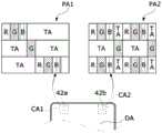
参照图24b,第二显示区域CA可包括:具有比第一显示区域DA数量少的像素的第一单位区域CA2;和具有比第一单位区域CA2数量少的像素的第二单位区域CA1。就是说,甚至在第二显示区域CA中分辨率也可不同。Referring to FIG. 24b, the second display area CA may include: a first unit area CA2 having a smaller number of pixels than the first display area DA; and a second unit area CA1 having a smaller number of pixels than the first unit area CA2. That is, the resolution may be different even in the second display area CA.
可在第二显示区域CA下方设置多个电子器件。作为示例,多个电子器件可包括确定周围亮度的环境光传感器(Ambient light sensor)、接近传感器(Proximity sensor)、内置有图像传感器的相机模块、以及接收红外光的红外传感器。相机模块42a包括红外滤波器,以阻断红外波段的光并且接收可见光,而红外传感器42b可接收红外波段的光。A plurality of electronic devices may be disposed under the second display area CA. As examples, the plurality of electronic devices may include an ambient light sensor to determine ambient brightness, a proximity sensor, a camera module with an image sensor built in, and an infrared sensor to receive infrared light. The
在此,与相机模块42a相比,即使当光量较小时红外传感器42b仍可进行相对精确的测量。因而,设置相机模块42a的第二单位区域CA1的像素数量可少于设置红外传感器42b的第一单位区域CA2的像素数量。Here, compared with the
作为示例,第二单位区域CA1的像素图案PA1可具有图24a中所示的像素图案,第一单位区域CA2的像素图案PA2可具有图20中所示的像素图案。作为示例,第一单位区域CA2可被设计为具有10%至30%的光透射率。因而,在第二单位区域CA1中入射光的量可相对较大。然而,这种像素图案不必限于此,可没有限制地应用本申请中描述的像素图案。As an example, the pixel pattern PA1 of the second unit area CA1 may have the pixel pattern shown in FIG. 24 a , and the pixel pattern PA2 of the first unit area CA2 may have the pixel pattern shown in FIG. 20 . As an example, the first unit area CA2 may be designed to have a light transmittance of 10% to 30%. Thus, the amount of incident light in the second unit area CA1 may be relatively large. However, such pixel patterns are not necessarily limited thereto, and the pixel patterns described in this application may be applied without limitation.
图25是图解根据本公开内容第十实施方式的第二显示区域中的像素布置的视图,图26是图25的放大图,图27是图解根据本公开内容第十一实施方式的第二显示区域中的像素布置的视图。25 is a view illustrating a pixel arrangement in a second display area according to a tenth embodiment of the present disclosure, FIG. 26 is an enlarged view of FIG. 25 , and FIG. 27 is a view illustrating a second display area according to an eleventh embodiment of the present disclosure. A view of the arrangement of pixels in a region.
参照图25,多个第二像素组PG2可设置在第一像素行RW1中,并且多个透光区域TA可设置在第二像素行RW2中。在这种情况下,像素的数量与第一显示区域DA相比减少1/2,使得足够多的光量可注入到传感器中。Referring to FIG. 25 , a plurality of second pixel groups PG2 may be disposed in the first pixel row RW1, and a plurality of light transmitting areas TA may be disposed in the second pixel row RW2. In this case, the number of pixels is reduced by 1/2 compared to the first display area DA, so that a sufficient amount of light can be injected into the sensor.
多个第二像素组PG2的第一至第四子像素SP1、SP2、SP3和SP4可设置在方形线P1、P2、P3和P4的每一个上。根据该布置,由于所有子像素均匀地设置,所以即使当与第一显示区域DA相比省略了一些像素,也可实现均匀的图像质量。此外,不会从外部观察到像素图案,使得可提高图像质量。The first to fourth sub-pixels SP1, SP2, SP3 and SP4 of the plurality of second pixel groups PG2 may be disposed on each of the square lines P1, P2, P3 and P4. According to this arrangement, even when some pixels are omitted compared with the first display area DA, uniform image quality can be achieved since all sub-pixels are uniformly arranged. In addition, pixel patterns are not observed from the outside, so that image quality can be improved.
参照图26,将第二发光元件G1和第四发光元件G2连接的第三虚拟线FL3可与第一方向平行。该像素布置与第一显示区域的像素步骤相同。Referring to FIG. 26 , a third imaginary line FL3 connecting the second light emitting element G1 and the fourth light emitting element G2 may be parallel to the first direction. The pixel arrangement is the same as the pixel step of the first display area.
与每个子像素连接的线TS可配置为避开透光区域TA。作为示例,与每个子像素连接的数据线、扫描线和EM线可被设计为尽可能地绕过透光区域TA。此外,阴极的与透光区域TA对应的部分可被图案化,以增加光透射率。The line TS connected to each sub-pixel may be configured to avoid the light-transmitting area TA. As an example, data lines, scan lines, and EM lines connected to each sub-pixel may be designed to bypass the light-transmitting area TA as much as possible. In addition, a portion of the cathode corresponding to the light transmission area TA may be patterned to increase light transmittance.
参照图27,多个第二像素组PG2可设置为沿第一方向彼此分隔开。与图25的沿第一方向连续设置的第二像素组PG2相比,透光区域TA设置在图27的多个第二像素组PG2之间,因而像素的数量可进一步减少。因此,光可充分地入射到增加的透光区域TA上。Referring to FIG. 27 , a plurality of second pixel groups PG2 may be arranged to be spaced apart from each other along the first direction. Compared with the second pixel group PG2 continuously arranged along the first direction of FIG. 25 , the light-transmitting area TA is disposed between the plurality of second pixel groups PG2 of FIG. 27 , and thus the number of pixels can be further reduced. Therefore, light may be sufficiently incident on the increased light transmission area TA.
设置在多个第二像素组PG2中的子像素SP1、SP2、SP3和SP4的每一个可设置在倾斜45°的方形线上。作为示例,多个第一子像素SP1可设置在第一方形线P1上,多个第二子像素SP2可设置在第二方形线P2上,多个第三子像素SP3可设置在第三方形线P3上,并且多个第四子像素SP4可设置在第四方形线P4上。Each of the sub-pixels SP1, SP2, SP3, and SP4 disposed in the plurality of second pixel groups PG2 may be disposed on a square line inclined at 45°. As an example, a plurality of first sub-pixels SP1 may be disposed on a first square line P1, a plurality of second sub-pixels SP2 may be disposed on a second square line P2, and a plurality of third sub-pixels SP3 may be disposed on a third square line P1. on the square line P3, and a plurality of fourth sub-pixels SP4 may be disposed on the fourth square line P4.
图28是图解根据本公开内容第十二实施方式的第二显示区域中的像素布置的视图。FIG. 28 is a view illustrating a pixel arrangement in a second display area according to a twelfth embodiment of the present disclosure.
图28图解了从图20的第二像素组PG2省略第四子像素SP4的结构。因此,第一至第三子像素SP1至SP3可实现为构成一个像素的真实型像素,但本公开内容不必限于此。FIG. 28 illustrates a structure in which the fourth sub-pixel SP4 is omitted from the second pixel group PG2 of FIG. 20 . Accordingly, the first to third sub-pixels SP1 to SP3 may be implemented as true type pixels constituting one pixel, but the present disclosure is not necessarily limited thereto.
图29是图解根据本公开内容第十三实施方式的第二显示区域中的像素布置的视图,图30是图解根据本公开内容第十四实施方式的第二显示区域中的像素布置的视图。29 is a view illustrating pixel arrangement in the second display area according to the thirteenth embodiment of the present disclosure, and FIG. 30 is a view illustrating the pixel arrangement in the second display area according to the fourteenth embodiment of the present disclosure.
参照图29,构成第二像素组PG2的多个子像素可设置在两个像素行RW1和RW2中。作为示例,第二子像素SP2和第三子像素SP3可设置在第一像素行RW1中,并且第一子像素SP1和第四子像素SP4可设置在第二像素行RW2中。Referring to FIG. 29 , a plurality of subpixels constituting the second pixel group PG2 may be disposed in two pixel rows RW1 and RW2 . As an example, the second subpixel SP2 and the third subpixel SP3 may be disposed in the first pixel row RW1, and the first subpixel SP1 and the fourth subpixel SP4 may be disposed in the second pixel row RW2.
透光区域TA可设置在第一像素行RW1中的第二子像素SP2与第三子像素SP3之间并且可设置在第二像素行RW2中的第一子像素SP1与第四子像素SP4之间。The light transmitting area TA may be disposed between the second sub-pixel SP2 and the third sub-pixel SP3 in the first pixel row RW1 and may be disposed between the first sub-pixel SP1 and the fourth sub-pixel SP4 in the second pixel row RW2. between.
多个第二像素组PG2可设置为沿第一方向彼此分隔开,但是可沿第二方向连续设置。然而,本公开内容不必限于此,多个第二像素组PG2也可设置为沿第二方向彼此分隔开。The plurality of second pixel groups PG2 may be disposed apart from each other in the first direction, but may be continuously disposed in the second direction. However, the present disclosure is not necessarily limited thereto, and a plurality of second pixel groups PG2 may also be arranged to be spaced apart from each other along the second direction.
参照图30,多个第二像素组PG2可包括具有不同像素布置的第2-1像素组PG21和第2-2像素组PG22。Referring to FIG. 30 , the plurality of second pixel groups PG2 may include a 2-1 pixel group PG21 and a 2-2 pixel group PG22 having different pixel arrangements.
作为示例,在第2-1像素组PG21中,第一子像素SP1和第二子像素SP2可设置在第二像素行RW2中,并且第三子像素SP3和第四子像素SP4可设置在第三像素行RW3中。As an example, in the 2-1 pixel group PG21, the first subpixel SP1 and the second subpixel SP2 may be disposed in the second pixel row RW2, and the third subpixel SP3 and the fourth subpixel SP4 may be disposed in the second pixel row RW2. three-pixel row RW3.
然而,在第2-2像素组PG22中,第二子像素SP2和第三子像素SP3可设置在第四像素行RW4中,并且第一子像素SP1和第四子像素SP4可设置在第五像素行RW5中。However, in the 2-2 pixel group PG22, the second subpixel SP2 and the third subpixel SP3 may be arranged in the fourth pixel row RW4, and the first subpixel SP1 and the fourth subpixel SP4 may be arranged in the fifth pixel row RW4. pixel row RW5.
就是说,在相邻的第二像素组PG2之间,绿色子像素的位置可相同,但是红色子像素和蓝色子像素的布置可不同。在这种情况下,相同颜色的子像素可沿第二斜线方向D2设置。就是说,多个第一子像素SP1可沿第二斜线方向D2设置,多个第二子像素SP2可沿第二斜线方向D2设置,多个第三子像素SP3可沿第二斜线方向D2设置,并且多个第四子像素SP4可沿第二斜线方向D2设置。That is, between adjacent second pixel groups PG2, the positions of the green sub-pixels may be the same, but the arrangement of the red and blue sub-pixels may be different. In this case, sub-pixels of the same color may be arranged along the second oblique direction D2. That is, the plurality of first sub-pixels SP1 may be arranged along the second oblique direction D2, the plurality of second sub-pixels SP2 may be arranged along the second oblique direction D2, and the plurality of third sub-pixels SP3 may be arranged along the second oblique direction D2. The direction D2 is arranged, and the plurality of fourth sub-pixels SP4 may be arranged along the second oblique direction D2.
图31是图解根据本公开内容第十五实施方式的第二显示区域中的像素布置的视图,图32是图解根据本公开内容第十六实施方式的第二显示区域中的像素布置的视图。31 is a view illustrating a pixel arrangement in a second display area according to a fifteenth embodiment of the present disclosure, and FIG. 32 is a view illustrating a pixel arrangement in a second display area according to a sixteenth embodiment of the present disclosure.
参照图31,红色子像素和蓝色子像素的位置与图30中相反地设置。因而,多个第一子像素SP1可沿第一斜线方向D1设置,多个第二子像素SP2可沿第一斜线方向D1设置,多个第三子像素SP3可沿第一斜线方向D1设置,并且多个第四子像素SP4可沿第一斜线方向D1设置。此外,如图32中所示,多个第二像素组PG2也可沿第二方向彼此分隔开。Referring to FIG. 31 , the positions of the red sub-pixel and the blue sub-pixel are set opposite to those in FIG. 30 . Therefore, the plurality of first sub-pixels SP1 may be arranged along the first oblique direction D1, the plurality of second sub-pixels SP2 may be arranged along the first oblique direction D1, and the plurality of third sub-pixels SP3 may be arranged along the first oblique direction. D1 is disposed, and a plurality of fourth sub-pixels SP4 may be disposed along the first oblique direction D1. In addition, as shown in FIG. 32 , the plurality of second pixel groups PG2 may also be spaced apart from each other along the second direction.
图33是图解根据本公开内容第十七实施方式的第二显示区域中的像素布置的视图。FIG. 33 is a view illustrating a pixel arrangement in a second display area according to a seventeenth embodiment of the present disclosure.
参照图33,构成第二像素组PG2的多个子像素可设置在两个像素行中。作为示例,第一子像素SP1和第二子像素SP2可设置在第一像素行RW1中,并且第三子像素SP3和第四子像素SP4可设置在第二像素行RW2中。Referring to FIG. 33 , a plurality of sub-pixels constituting the second pixel group PG2 may be disposed in two pixel rows. As an example, the first subpixel SP1 and the second subpixel SP2 may be disposed in the first pixel row RW1, and the third subpixel SP3 and the fourth subpixel SP4 may be disposed in the second pixel row RW2.
第一子像素SP1和第二子像素SP2可构成第一单位像素PIX1,第三子像素SP3和第四子像素SP4可构成第二单位像素PIX2。在此,第一单位像素PIX1和第二单位像素PIX2可设置为彼此偏移,从而在第二方向上不重叠。The first sub-pixel SP1 and the second sub-pixel SP2 may constitute the first unit pixel PIX1, and the third sub-pixel SP3 and the fourth sub-pixel SP4 may constitute the second unit pixel PIX2. Here, the first unit pixel PIX1 and the second unit pixel PIX2 may be disposed offset from each other so as not to overlap in the second direction.
图34是图解根据本公开内容实施方式的显示面板和显示面板驱动单元的框图,图35是图解驱动器集成电路(IC)的配置的示意性框图。34 is a block diagram illustrating a display panel and a display panel driving unit according to an embodiment of the present disclosure, and FIG. 35 is a schematic block diagram illustrating a configuration of a driver integrated circuit (IC).
参照图34和图35,显示装置可包括:具有设置于屏幕上的像素阵列的显示面板100、显示面板驱动单元等。Referring to FIGS. 34 and 35 , the display device may include a
显示面板100的像素阵列可包括数据线DL、与数据线DL交叉的栅极线GL、以及以由数据线DL和栅极线GL限定的矩阵形式布置的像素P。The pixel array of the
在显示面板100中,再现输入图像的屏幕可包括第一显示区域DA和第二显示区域CA。In the
第一显示区域DA和第二显示区域CA的每一个的子像素可包括像素电路。像素电路可包括:配置为给发光元件OLED提供电流的驱动元件、配置为采样驱动元件的阈值电压并且切换像素电路的电流路径(current path)的多个开关元件、配置为保持驱动元件的栅极电压的电容器等。像素电路可设置在发光元件下方。The sub-pixels of each of the first display area DA and the second display area CA may include a pixel circuit. The pixel circuit may include: a driving element configured to supply current to the light emitting element OLED, a plurality of switching elements configured to sample a threshold voltage of the driving element and switch a current path of the pixel circuit, a gate configured to hold the driving element voltage capacitors, etc. A pixel circuit may be disposed under the light emitting element.
第二显示区域CA可包括设置在像素组之间的透光区域TA和设置在第二显示区域CA下方的相机模块400。在成像模式中,相机模块400可使用图像传感器对通过第二显示区域CA入射的光进行光电转换并且将从图像传感器输出的图像的像素数据转换为数字数据,以输出成像的图像数据。The second display area CA may include a light transmission area TA disposed between pixel groups and a
显示面板驱动单元可对像素P写入输入图像的像素数据。像素P可解释为包括多个子像素的像素组。The display panel driving unit may write pixel data of an input image to the pixel P. A pixel P can be interpreted as a pixel group including a plurality of sub-pixels.
显示面板驱动单元可包括:配置为给数据线DL提供像素数据的数据电压的数据驱动单元306、以及配置为给栅极线GL顺序地提供栅极脉冲的栅极驱动单元120。数据驱动单元306可被集成到驱动器IC 300中。显示面板驱动单元可进一步包括图中省略的触摸传感器驱动单元。The display panel driving unit may include a
驱动器IC 300可附接至显示面板100。驱动器IC 300从主机系统200接收输入图像的像素数据和时序信号,将像素数据的数据电压提供至像素,并且将数据驱动单元306与栅极驱动单元120同步。The
驱动器IC 300可通过数据输出通道连接至数据线DL,以将像素数据的数据电压提供至数据线DL。驱动器IC 300可通过栅极时序信号输出通道输出用于控制栅极驱动单元120的栅极时序信号。The
从时序控制器303产生的栅极时序信号可包括栅极起始脉冲(Gate start pulse,VST)、栅极移位时钟(Gate shift clock,CLK)等。栅极起始脉冲VST和栅极移位时钟CLK可在栅极导通电压VGL与栅极截止电压VGH之间摆动(swing)。The gate timing signal generated from the
从电平转换器307输出的栅极时序信号(VST和CLK)可施加至栅极驱动单元120,以控制栅极驱动单元120的移位操作。The gate timing signals (VST and CLK) output from the
栅极驱动单元120可包括与像素阵列一起形成在显示面板100的电路层上的移位寄存器(shift register)。栅极驱动单元120的移位寄存器可在时序控制器的控制下给栅极线GL顺序地提供栅极信号。栅极信号可包括扫描脉冲和发光信号的EM脉冲。The
移位寄存器可包括:配置为输出扫描脉冲的扫描驱动单元、以及配置为输出EM脉冲的EM驱动单元。在图35中,“GVST”和“GCLK”是输入到扫描驱动单元的栅极时序信号中包括的信号。“EVST”和“ECLK”是输入到EM驱动单元的栅极时序信号中包括的信号。The shift register may include: a scan driving unit configured to output scan pulses, and an EM driving unit configured to output EM pulses. In FIG. 35 , "GVST" and "GCLK" are signals included in gate timing signals input to the scan driving unit. "EVST" and "ECLK" are signals included in gate timing signals input to the EM drive unit.
驱动器IC 300可连接至主机系统200、第一存储器301和显示面板100。驱动器IC300可包括数据接收和计算单元308、时序控制器303、数据驱动单元306、伽马补偿电压产生单元305、电源单元304、第二存储器302等。The
数据接收和计算单元308可包括:配置为接收从主机系统200作为数字信号输入的像素数据的接收单元、以及配置为处理通过接收单元输入的像素数据以提高图像质量的数据计算单元。The data reception and
数据计算单元可包括:配置为通过将压缩的像素数据解码(Decoding)来执行恢复的数据恢复单元、配置为对像素数据增加预设的光学补偿值的光学补偿单元等。光学补偿值可设为用于根据以制造工序中拍摄的相机图像为基准测量的屏幕的亮度来校正各条像素数据的值。The data calculation unit may include: a data restoration unit configured to perform restoration by decoding (Decoding) the compressed pixel data, an optical compensation unit configured to add a preset optical compensation value to the pixel data, and the like. The optical compensation value can be set as a value for correcting each piece of pixel data based on the luminance of the screen measured based on the camera image taken in the manufacturing process.
时序控制器303可给数据驱动单元306提供从主机系统200接收的输入图像的像素数据。时序控制器303可产生用于控制栅极驱动单元120的栅极时序信号和用于控制数据驱动单元306的源极时序信号,以控制栅极驱动单元120和数据驱动单元306的操作时序。The
数据驱动单元306可使用数模转换器(Digital to Analog converter,DAC)将从时序控制器303接收的包括像素数据的数字数据转换为伽马补偿电压并且输出数据电压。从数据驱动单元306输出的数据电压可通过与驱动器IC 300的数据通道连接的输出缓冲器提供至像素阵列的数据线DL。The
伽马补偿电压产生单元305可通过经由分压器电路分割从电源单元304接收的伽马基准电压来产生每个灰度的伽马补偿电压。伽马补偿电压是其中对像素数据的每个灰度设定电压的模拟电压。从伽马补偿电压产生单元305输出的伽马补偿电压可提供至数据驱动单元306。The gamma compensation
电源单元304可使用DC-DC转换器(DC-DC Converter)产生驱动驱动器IC 300、栅极驱动单元120和显示面板100的像素阵列所需的电力。DC-DC转换器可包括电荷泵(Chargepump)、调节器(Regulator)、降压转换器(Buck Converter)、升压转换器(BoostConverter)等。The
电源单元304可通过调整从主机系统200接收的DC输入电压产生DC电压,诸如伽马基准电压、栅极导通电压VGL、栅极截止电压VGH、像素驱动电压VDD、低电位电源电压VSS、初始化电压Vini等。The
伽马基准电压可提供至伽马补偿电压产生单元305。栅极导通电压VGL和栅极截止电压VGH可提供至电平转换器307和栅极驱动单元120。诸如像素驱动电压VDD、低电位电源电压VSS和初始化电压Vini之类的像素电源电压可公共地提供至像素P。The gamma reference voltage may be provided to the gamma compensation
初始化电压Vini可设为比像素驱动电压VDD低并且比发光元件OLED的阈值电压低的DC电压,以将像素电路的主要节点初始化并且抑制发光元件OLED的发光。The initialization voltage Vini may be set to a DC voltage lower than the pixel driving voltage VDD and lower than a threshold voltage of the light emitting element OLED to initialize main nodes of the pixel circuit and suppress light emission of the light emitting element OLED.
当电力提供至驱动器IC 300时,第二存储器302可存储从第一存储器301接收的补偿值、寄存器设定数据等。The
补偿值可应用于提高图像质量的各种算法。补偿值可包括光学补偿值。寄存器设定数据可定义数据驱动单元306、时序控制器303、伽马补偿电压产生单元305等的操作。第一存储器301可包括闪存(Flash memory)。第二存储器302可包括静态随机存取存储器(Static RAM,SRAM)。Compensation values can be applied to various algorithms that improve image quality. The compensation value may include an optical compensation value. The register setting data may define the operations of the
主机系统200可实现为应用处理器(Application Processor,AP)。主机系统200可通过移动产业处理器接口(Mobile Industry Processor Interface,MIPI)将输入图像的像素数据传送至驱动器IC 300。主机系统200可通过例如柔性印刷电路(Flexible PrintedCircuit,FPC)连接至驱动器IC 300。The
另外,显示面板可实现为可应用于柔性显示器的柔性面板。柔性显示器可通过卷绕、折叠或弯折柔性面板而具有尺寸变化的屏幕并且可容易以各种设计进行制造。In addition, the display panel may be implemented as a flexible panel applicable to flexible displays. A flexible display can have a size-changing screen by rolling, folding, or bending a flexible panel and can be easily manufactured in various designs.
柔性显示器可实现为可卷绕显示器(rollable display)、可折叠显示器(foldable display)、可弯折(bendable)显示器、可滑动显示器(slidable display)等。The flexible display may be implemented as a rollable display, a foldable display, a bendable display, a slidable display, and the like.
柔性面板可被制造为所谓的“塑料OLED面板”。塑料OLED面板可包括背板(Backplate)和形成在附接至背板的有机薄膜上的像素阵列。可在像素阵列上形成触摸传感器阵列。Flexible panels can be manufactured as so-called "plastic OLED panels". A plastic OLED panel may include a backplate (Backplate) and a pixel array formed on an organic film attached to the backplate. A touch sensor array may be formed on the pixel array.
背板可以是聚对苯二甲酸乙二醇酯(Polyethylene terephthalate,PET)基板。像素阵列和触摸传感器阵列可形成在有机薄膜上。背板可阻挡湿气渗透到有机薄膜,使得像素阵列不暴露于湿气。The backsheet may be a polyethylene terephthalate (PET) substrate. Pixel arrays and touch sensor arrays can be formed on organic thin films. The backplane blocks moisture from penetrating the organic film, so that the pixel array is not exposed to moisture.
有机薄膜可以是聚酰亚胺(Polyimide,PI)基板。可在有机薄膜上由绝缘材料(未示出)形成多层缓冲膜。电路层12和发光元件层14可堆叠在有机薄膜上。The organic thin film may be a polyimide (Polyimide, PI) substrate. A multilayer buffer film may be formed of an insulating material (not shown) on the organic thin film. The
在本公开内容的显示装置中,设置在电路层12上的像素电路和栅极驱动单元可包括多个晶体管。晶体管可实现为包括氧化物半导体的氧化物薄膜晶体管(Oxide Thin FilmTransistor,Oxide TFT)、包括低温多晶硅(Low Temperature Poly Silicon,LTPS)的LTPSTFT等。每个晶体管可实现为p沟道薄膜晶体管(TFT)或n沟道TFT。将关注于像素电路的晶体管实现为p沟道TFT的示例描述下面的实施方式,但本公开内容不限于此。In the display device of the present disclosure, the pixel circuit and the gate driving unit disposed on the
晶体管是包括栅极(gate)、源极(source)和漏极(drain)的三电极元件。源极是给晶体管提供载流子(carrier)的电极。晶体管中的载流子可从源极开始流动。漏极是供载流子从晶体管离开到外部的电极。A transistor is a three-electrode element including a gate, a source, and a drain. The source is an electrode that provides carriers to the transistor. Carriers in a transistor can flow from the source. The drain is an electrode for the exit of carriers from the transistor to the outside.
在晶体管中,载流子从源极流动到漏极。在n沟道晶体管的情况下,载流子是电子(electron),因而源极电压低于漏极电压,使得电子从源极流动到漏极。在n沟道晶体管的情况下,电流从漏极流动到源极。In a transistor, carriers flow from source to drain. In the case of an n-channel transistor, the carriers are electrons, so the source voltage is lower than the drain voltage, allowing electrons to flow from the source to the drain. In the case of n-channel transistors, current flows from the drain to the source.
在p沟道晶体管(PMOS)的情况下,载流子是空穴(hole),因而源极电压高于漏极电压,使得空穴从源极流动到漏极。在p沟道晶体管的情况下,由于空穴从源极流动到漏极,所以电流从源极流动到漏极。应当注意,晶体管的源极和漏极的位置不是固定的。例如,源极和漏极可根据施加的电压互换。因此,本公开内容不受晶体管的源极和漏极限制。在下面的描述中,晶体管的源极和漏极将被称为第一电极和第二电极。In the case of a p-channel transistor (PMOS), the carriers are holes, so the source voltage is higher than the drain voltage, allowing the holes to flow from the source to the drain. In the case of p-channel transistors, as holes flow from source to drain, current flows from source to drain. It should be noted that the positions of the source and drain of the transistor are not fixed. For example, source and drain can be interchanged depending on the applied voltage. Therefore, the present disclosure is not limited by the sources and drains of transistors. In the following description, the source and drain of the transistor will be referred to as a first electrode and a second electrode.
栅极脉冲可在栅极导通电压(Gate On Voltage)与栅极截止电压(Gate OffVoltage)之间摆动(swing)。栅极导通电压可设为高于晶体管的阈值电压,栅极截止电压可设为低于晶体管的阈值电压。The gate pulse can swing between a gate on voltage (Gate On Voltage) and a gate off voltage (Gate Off Voltage). The gate-on voltage can be set higher than the threshold voltage of the transistor, and the gate-off voltage can be set lower than the threshold voltage of the transistor.
晶体管可响应于栅极导通电压导通(turn-on)并且响应于栅极截止电压截止(turn-off)。在n沟道晶体管的情况下,栅极导通电压可以是栅极高电压(Gate HighVoltage,VGH),栅极截止电压可以是栅极低电压(Gate Low Voltage,VGL)。在p沟道晶体管的情况下,栅极导通电压可以是VGL,栅极截止电压可以是VGH。The transistor is turn-on in response to a gate-on voltage and turn-off in response to a gate-off voltage. In the case of an n-channel transistor, the gate-on voltage may be a gate high voltage (Gate High Voltage, VGH), and the gate-off voltage may be a gate low voltage (Gate Low Voltage, VGL). In the case of a p-channel transistor, the gate-on voltage may be VGL, and the gate-off voltage may be VGH.
像素电路的驱动元件可实现为晶体管。驱动元件应在所有像素之间具有均匀的电特性,但是由于工艺变化和元件特性变化,在像素之间会具有电特性的差异,并且显示驱动时间流逝,电特性会变化。The driving elements of the pixel circuit may be implemented as transistors. The driving element should have uniform electrical characteristics among all pixels, but due to process variations and element characteristic variations, there will be differences in electrical characteristics between pixels, and the electrical characteristics will vary with the lapse of display driving time.
为了补偿驱动元件的电特性变化,显示装置可包括内部补偿电路和外部补偿电路。内部补偿电路可被添加到每个子像素中的像素电路,以采样根据驱动元件的电特性而变化的驱动元件的阈值电压Vth和/或迁移率μ,并且实时补偿所述变化。In order to compensate for variations in electrical characteristics of driving elements, a display device may include an internal compensation circuit and an external compensation circuit. An internal compensation circuit may be added to the pixel circuit in each sub-pixel to sample threshold voltage Vth and/or mobility μ of a driving element that varies according to electrical characteristics of the driving element, and compensate for the variation in real time.
外部补偿电路可将通过与每个子像素连接的感测线感测的驱动元件的阈值电压和/或迁移率传送到外部补偿单元。外部补偿电路的补偿单元可反映感测结果来调制输入图像的像素数据,从而补偿驱动元件的电特性的变化。The external compensation circuit may transmit the threshold voltage and/or mobility of the driving element sensed through the sensing line connected to each sub-pixel to the external compensation unit. The compensation unit of the external compensation circuit may reflect the sensing result to modulate the pixel data of the input image, thereby compensating for the variation of the electrical characteristics of the driving element.
可感测根据外部补偿驱动元件的电特性而变化的像素的电压,并且基于感测的电压在外部电路中调制输入图像的数据,从而补偿像素之间的驱动元件的电特性的变化。A voltage of a pixel varying according to an electrical characteristic of an externally compensating driving element may be sensed, and data of an input image is modulated in an external circuit based on the sensed voltage, thereby compensating for variation in the electrical characteristic of the driving element between pixels.
图36是图解像素电路的一示例的电路图,图37是图解像素电路的另一示例的电路图。图38是图解驱动图36和图37中所示的像素电路的方法的视图。FIG. 36 is a circuit diagram illustrating an example of a pixel circuit, and FIG. 37 is a circuit diagram illustrating another example of a pixel circuit. FIG. 38 is a view illustrating a method of driving the pixel circuits shown in FIGS. 36 and 37 .
图36和图37中所示的像素电路可相似地应用于第一显示区域DA和第二显示区域CA的像素电路。可应用于本公开内容的像素电路可实现为图36和图37中所示的电路,但本公开内容不限于此。The pixel circuits shown in FIGS. 36 and 37 may be similarly applied to the pixel circuits of the first display area DA and the second display area CA. A pixel circuit applicable to the present disclosure may be realized as the circuits shown in FIGS. 36 and 37 , but the present disclosure is not limited thereto.
参照图36至图38,像素电路可包括发光元件OLED、配置为给发光元件OLED提供电流的驱动元件DT、以及内部补偿电路,内部补偿电路配置为使用多个开关元件M1至M6采样驱动元件DT的阈值电压Vth并且将驱动元件DT的栅极电压补偿驱动元件DT的阈值电压Vth。驱动元件DT和开关元件M1至M6的每一个可实现为p沟道TFT。Referring to FIGS. 36 to 38 , the pixel circuit may include a light emitting element OLED, a driving element DT configured to supply current to the light emitting element OLED, and an internal compensation circuit configured to sample the driving element DT using a plurality of switching elements M1 to M6. The threshold voltage Vth of the driving element DT is compensated by the gate voltage of the driving element DT to the threshold voltage Vth of the driving element DT. Each of the driving element DT and the switching elements M1 to M6 can be realized as a p-channel TFT.
使用内部补偿电路的像素电路的驱动时段可分为初始化时段Tini、采样时段Tsam、数据写入时段Twr和发光时段Tem,如图38中所示。The driving period of the pixel circuit using the internal compensation circuit can be divided into an initialization period Tini, a sampling period Tsam, a data writing period Twr, and a light emission period Tem, as shown in FIG. 38 .
在初始化时段Tini期间,第N-1扫描信号SCAN(N-1)被生成为栅极导通电压VGL的脉冲,并且第N扫描信号SCAN(N)和发光信号EM(N)的每一个的电压是栅极截止电压VGH。在采样时段Tsam期间,第N扫描信号SCAN(N)被生成为栅极导通电压VGL的脉冲,并且第N-1扫描信号SCAN(N-1)和发光信号EM(N)的每一个的电压是栅极截止电压VGH。在数据写入时段Twr期间,第N-1扫描信号SCAN(N-1)、第N扫描信号SCAN(N)和发光信号EM(N)的每一个的电压是栅极截止电压VGH。在发光时段Tem的至少部分时段期间,发光信号EM(N)可被生成为栅极导通电压VGL,并且第N-1扫描信号SCAN(N-1)和第N扫描信号SCAN(N)的每一个电压可被生成为栅极截止电压VGH。During the initialization period Tini, the N-1th scan signal SCAN(N-1) is generated as a pulse of the gate-on voltage VGL, and each of the Nth scan signal SCAN(N) and the light emitting signal EM(N) The voltage is the gate-off voltage VGH. During the sampling period Tsam, the N-th scan signal SCAN(N) is generated as a pulse of the gate-on voltage VGL, and each of the N-1-th scan signal SCAN(N-1) and the light emission signal EM(N) The voltage is the gate-off voltage VGH. During the data writing period Twr, the voltage of each of the N-1th scan signal SCAN(N-1), the Nth scan signal SCAN(N), and the light emission signal EM(N) is the gate-off voltage VGH. During at least a part of the light emission period Tem, the light emission signal EM(N) may be generated as the gate-on voltage VGL, and the N-1th scan signal SCAN(N-1) and the Nth scan signal SCAN(N) Each voltage may be generated as a gate-off voltage VGH.
在初始化时段Tini期间,第五开关元件M5可根据第N-1扫描信号SCAN(N-1)的栅极导通电压VGL导通,以将像素电路初始化。在采样时段Tsam期间,第一开关元件M1和第二开关元件M2可根据第N扫描信号SCAN(N)的栅极导通电压VGL导通,使得驱动元件DT的阈值电压可被采样并存储在存储电容器Cst1中。同时,第六开关元件M6可在采样时段Tsam期间导通,以将第四节点n4的电压降低至基准电压Vref,从而抑制发光元件OLED的发光。在数据写入时段Twr期间,第一至第六开关元件M1至M6可保持在截止状态。在发光时段Tem期间,第三开关元件M3和第四开关元件M4可导通,使得发光元件OLED发光。在发光时段Tem中,为了利用发光信号EM(N)的占空比(duty ration)精确地呈现低灰度的亮度,发光信号EM(N)可以以预定的占空比在栅极导通电压VGL与栅极截止电压VGH之间摆动,以重复第三开关元件M3和第四开关元件M4的导通或截止。During the initialization period Tini, the fifth switching element M5 may be turned on according to the gate-on voltage VGL of the N-1th scan signal SCAN(N-1) to initialize the pixel circuit. During the sampling period Tsam, the first switching element M1 and the second switching element M2 may be turned on according to the gate-on voltage VGL of the Nth scan signal SCAN(N), so that the threshold voltage of the driving element DT may be sampled and stored in storage capacitor Cst1. Meanwhile, the sixth switching element M6 may be turned on during the sampling period Tsam to reduce the voltage of the fourth node n4 to the reference voltage Vref, thereby suppressing the light emission of the light emitting element OLED. During the data writing period Twr, the first to sixth switching elements M1 to M6 may be maintained in a turn-off state. During the light emitting period Tem, the third switching element M3 and the fourth switching element M4 may be turned on so that the light emitting element OLED emits light. In the light-emitting period Tem, in order to accurately present low-gray-scale luminance by using the duty ratio of the light-emitting signal EM(N), the light-emitting signal EM(N) can be turned on at the gate voltage at a predetermined duty ratio. VGL swings between the gate-off voltage VGH to repeatedly turn on or off the third switching element M3 and the fourth switching element M4.
发光元件OLED可实现为有机发光二极管或无机发光二极管。下文中,将描述发光元件OLED实现为有机发光二极管的示例。The light emitting element OLED can be realized as an organic light emitting diode or an inorganic light emitting diode. Hereinafter, an example in which the light emitting element OLED is realized as an organic light emitting diode will be described.
发光元件OLED可包括形成在阳极与阴极之间的有机化合物层。有机化合物层可包括空穴注入层HIL、空穴传输层HTL、发光层EML、电子传输层ETL和电子注入层EIL,但本公开内容不限于此。当电压施加至OLED的阳极和阴极时,穿过空穴传输层HTL的空穴和穿过电子传输层ETL的电子移动到发光层EML以产生激子,因而可从发光层EML发射可见光。The light emitting element OLED may include an organic compound layer formed between an anode and a cathode. The organic compound layer may include a hole injection layer HIL, a hole transport layer HTL, an emission layer EML, an electron transport layer ETL, and an electron injection layer EIL, but the present disclosure is not limited thereto. When a voltage is applied to the anode and cathode of the OLED, holes passing through the hole transport layer HTL and electrons passing through the electron transport layer ETL move to the emission layer EML to generate excitons, and thus visible light can be emitted from the emission layer EML.
发光元件OLED的阳极可连接至第四开关元件M4与第六开关元件M6之间的第四节点n4。第四节点n4连接至发光元件OLED的阳极、第四开关元件M4的第二电极和第六开关元件M6的第二电极。发光元件OLED的阴极可连接至被施加低电位电源电压VSS的VSS线PL3。发光元件OLED可利用根据驱动元件DT的栅极-源极电压Vgs而流动的电流Ids发光。第三开关元件M3和第四开关元件M4可切换发光元件OLED的电流路径。An anode of the light emitting element OLED may be connected to a fourth node n4 between the fourth switching element M4 and the sixth switching element M6. The fourth node n4 is connected to the anode of the light emitting element OLED, the second electrode of the fourth switching element M4, and the second electrode of the sixth switching element M6. A cathode of the light emitting element OLED may be connected to a VSS line PL3 to which a low-potential power supply voltage VSS is applied. The light emitting element OLED may emit light using the current Ids flowing according to the gate-source voltage Vgs of the driving element DT. The third switching element M3 and the fourth switching element M4 can switch the current path of the light emitting element OLED.
存储电容器Cst1可连接在VDD线PL1与第一节点n1之间。存储电容器Cst1可被充电上被补偿了驱动元件DT的阈值电压Vth的数据电压Vdata。由于每个子像素中的数据电压Vdata被补偿了驱动元件DT的阈值电压Vth,所以每个子像素中的驱动元件DT的特性偏差可被补偿。The storage capacitor Cst1 may be connected between the VDD line PL1 and the first node n1. The storage capacitor Cst1 may be charged with the data voltage Vdata compensated for the threshold voltage Vth of the driving element DT. Since the data voltage Vdata in each sub-pixel is compensated by the threshold voltage Vth of the driving element DT, a characteristic deviation of the driving element DT in each sub-pixel may be compensated.
第一开关元件M1可响应于第N扫描信号SCAN(N)的栅极导通电压VGL导通,以将第二节点n2连接至第三节点n3。第二节点n2可连接至驱动元件DT的栅极电极、存储电容器Cst1的第一电极和第一开关元件M1的第一电极。第三节点n3可连接至驱动元件DT的第二电极、第一开关元件M1的第二电极和第四开关元件M4的第一电极。第一开关元件M1的栅极电极连接至第一栅极线GL1,以接收第N扫描信号SCAN(N)。第一开关元件M1的第一电极可连接至第二节点n2,并且第一开关元件M1的第二电极可连接至第三节点n3。The first switching element M1 may be turned on in response to the gate-on voltage VGL of the Nth scan signal SCAN(N) to connect the second node n2 to the third node n3. The second node n2 may be connected to the gate electrode of the driving element DT, the first electrode of the storage capacitor Cst1, and the first electrode of the first switching element M1. The third node n3 may be connected to the second electrode of the driving element DT, the second electrode of the first switching element M1, and the first electrode of the fourth switching element M4. The gate electrode of the first switching element M1 is connected to the first gate line GL1 to receive the Nth scan signal SCAN(N). A first electrode of the first switching element M1 may be connected to the second node n2, and a second electrode of the first switching element M1 may be connected to the third node n3.
第一开关元件M1可在一个帧时段中的、其中第N扫描信号SCAN(N)被生成为栅极导通电压VGL的一个非常短的水平时段1H中导通,因而可在大约一个帧时段中保持在截止状态,因此在第一开关元件M1的截止状态中可能产生漏电流。为了抑制第一开关元件M1的漏电流,第一开关元件M1可实现为具有串联连接的两个晶体管M1a和M1b的双栅(dual-gate)结构,如图37中所示。The first switching element M1 can be turned on in a very short horizontal period 1H in which the N-th scan signal SCAN(N) is generated as the gate-on voltage VGL in one frame period, and thus can be turned on for about one frame period. is kept in an off state, and thus leakage current may be generated in the off state of the first switching element M1. In order to suppress the leakage current of the first switching element M1, the first switching element M1 may be realized in a dual-gate structure having two transistors M1a and M1b connected in series, as shown in FIG. 37 .
第二开关元件M2可响应于第N扫描信号SCAN(N)的栅极导通电压VGL导通,以将数据电压Vdata提供至第一节点n1。第二开关元件M2的栅极电极可连接至第一栅极线GL1,以接收第N扫描信号SCAN(N)。第二开关元件M2的第一电极可连接至第一节点n1。第二开关元件M2的第二电极可连接至被施加数据电压Vdata的数据线DL。第一节点n1可连接至第二开关元件M2的第一电极、第三开关元件M3的第二电极和驱动元件DT的第一电极。The second switching element M2 may be turned on in response to the gate-on voltage VGL of the Nth scan signal SCAN(N) to supply the data voltage Vdata to the first node n1. A gate electrode of the second switching element M2 may be connected to the first gate line GL1 to receive the Nth scan signal SCAN(N). A first electrode of the second switching element M2 may be connected to the first node n1. The second electrode of the second switching element M2 may be connected to the data line DL to which the data voltage Vdata is applied. The first node n1 may be connected to a first electrode of the second switching element M2, a second electrode of the third switching element M3, and a first electrode of the driving element DT.
第三开关元件M3可响应于发光信号EM(N)的栅极导通电压VGL导通,以将VDD线PL1连接至第一节点n1。第三开关元件M3的栅极电极可连接至第三栅极线GL3,以接收发光信号EM(N)。第三开关元件M3的第一电极可连接至VDD线PL1。第三开关元件M3的第二电极可连接至第一节点n1。The third switching element M3 may be turned on in response to the gate-on voltage VGL of the light emitting signal EM(N) to connect the VDD line PL1 to the first node n1. A gate electrode of the third switching element M3 may be connected to the third gate line GL3 to receive the light emitting signal EM(N). A first electrode of the third switching element M3 may be connected to the VDD line PL1. A second electrode of the third switching element M3 may be connected to the first node n1.
第四开关元件M4可响应于发光信号EM(N)的栅极导通电压VGL导通,以将第三节点n3连接至发光元件OLED的阳极。第四开关元件M4的栅极电极可连接至第三栅极线GL3,以接收发光信号EM(N)。第四开关元件M4的第一电极可连接至第三节点n3,并且第四开关元件M4的第二电极可连接至第四节点n4。The fourth switching element M4 may be turned on in response to the gate-on voltage VGL of the light emitting signal EM(N) to connect the third node n3 to the anode of the light emitting element OLED. A gate electrode of the fourth switching element M4 may be connected to the third gate line GL3 to receive the light emitting signal EM(N). A first electrode of the fourth switching element M4 may be connected to the third node n3, and a second electrode of the fourth switching element M4 may be connected to the fourth node n4.
第五开关元件M5可响应于第N-1扫描信号SCAN(N-1)的栅极导通电压VGL导通,以将第二节点n2连接至Vini线PL2。第五开关元件M5的栅极电极可连接至第二栅极线GL2,以接收第N-1扫描信号SCAN(N-1)。第五开关元件M5的第一电极可连接至第二节点n2,并且第五开关元件M5的第二电极可连接至Vini线PL2。为了抑制第五开关元件M5的漏电流,第五开关元件M5可实现为具有串联连接的两个晶体管M5a和M5b的双栅(结构,如图37中所示。The fifth switching element M5 may be turned on in response to the gate-on voltage VGL of the N-1th scan signal SCAN(N-1) to connect the second node n2 to the Vini line PL2. A gate electrode of the fifth switching element M5 may be connected to the second gate line GL2 to receive the N-1th scan signal SCAN(N-1). A first electrode of the fifth switching element M5 may be connected to the second node n2, and a second electrode of the fifth switching element M5 may be connected to the Vini line PL2. In order to suppress the leakage current of the fifth switching element M5, the fifth switching element M5 may be implemented as a double gate (structure) having two transistors M5a and M5b connected in series, as shown in FIG. 37 .
第六开关元件M6可响应于第N扫描信号SCAN(N)的栅极导通电压VGL导通,以将Vini线PL2连接至第四节点n4。第六开关元件M6的栅极电极可连接至第一栅极线GL1,以接收第N扫描信号SCAN(N)。第六开关元件M6的第一电极可连接至Vini线PL2,并且第六开关元件M6的第二电极可连接至第四节点n4。The sixth switching element M6 may be turned on in response to the gate-on voltage VGL of the Nth scan signal SCAN(N) to connect the Vini line PL2 to the fourth node n4. A gate electrode of the sixth switching element M6 may be connected to the first gate line GL1 to receive the Nth scan signal SCAN(N). A first electrode of the sixth switching element M6 may be connected to the Vini line PL2, and a second electrode of the sixth switching element M6 may be connected to the fourth node n4.
驱动元件DT可根据栅极-源极电压Vgs调节流入发光元件OLED中的电流Ids,以驱动发光元件OLED。驱动元件DT可包括连接至第二节点n2的栅极电极、连接至第一节点n1的第一电极、和连接至第三节点n3的第二电极。The driving element DT can adjust the current Ids flowing into the light emitting element OLED according to the gate-source voltage Vgs to drive the light emitting element OLED. The driving element DT may include a gate electrode connected to the second node n2, a first electrode connected to the first node n1, and a second electrode connected to the third node n3.
如图38中所示,第N-1扫描信号SCAN(N-1)在初始化时段Tini期间被生成为栅极导通电压VGL。在初始化时段Tini期间,第N扫描信号SCAN(N)和发光信号EM(N)可保持在栅极截止电压VGH。因而,在初始化时段Tini期间,第五开关元件M5可导通(turn-on),使得第二节点n2和第四节点n4各自可被初始化为“Vini”。可在初始化时段Tini与采样时段Tsam之间设定保持时段Th。在保持时段Th期间,栅极信号SCAN(N-1)、SCAN(N)和EM(N)可保持在它们之前的状态。As shown in FIG. 38 , the N-1th scan signal SCAN(N-1) is generated as the gate-on voltage VGL during the initialization period Tini. During the initialization period Tini, the Nth scan signal SCAN(N) and the light emitting signal EM(N) may be maintained at the gate-off voltage VGH. Thus, during the initialization period Tini, the fifth switching element M5 may be turned on (turn-on), so that each of the second node n2 and the fourth node n4 may be initialized to "Vini". The hold period Th can be set between the initialization period Tini and the sampling period Tsam. During the holding period Th, the gate signals SCAN(N−1), SCAN(N), and EM(N) may be maintained in their previous states.
在采样时段Tsam期间,第N扫描信号SCAN(N)可被生成为栅极导通电压VGL。第N扫描信号SCAN(N)可与第N像素线的数据电压Vdata同步。在采样时段Tsam期间,第N-1扫描信号SCAN(N-1)和发光信号EM(N)各自可保持在栅极截止电压。因而,在采样时段Tsam期间,第一开关元件M1和第二开关元件M2可导通。During the sampling period Tsam, the N-th scan signal SCAN(N) may be generated as the gate-on voltage VGL. The Nth scan signal SCAN(N) may be synchronized with the data voltage Vdata of the Nth pixel line. During the sampling period Tsam, each of the N-1th scan signal SCAN(N-1) and the emission signal EM(N) may be maintained at the gate-off voltage. Thus, during the sampling period Tsam, the first switching element M1 and the second switching element M2 may be turned on.
在采样时段Tsam期间,驱动元件DT的栅极电压DTG可由于流过第一开关元件M1和第二开关元件M2的电流而升高。当驱动元件DT截止时,栅极电压DTG是Vdata-|Vth|。在这种情况下,第一节点n1的电压也为Vdata-|Vth|。在采样时段Tsam期间,驱动元件DT的栅极-源极电压Vgs为|Vgs|=Vdata-(Vdata-|Vth|)=|Vth|。During the sampling period Tsam, the gate voltage DTG of the driving element DT may increase due to the current flowing through the first switching element M1 and the second switching element M2. When the driving element DT is turned off, the gate voltage DTG is Vdata-|Vth|. In this case, the voltage of the first node n1 is also Vdata-|Vth|. During the sampling period Tsam, the gate-source voltage Vgs of the driving element DT is |Vgs|=Vdata-(Vdata-|Vth|)=|Vth|.
在数据写入时段Twr期间,第N扫描信号SCAN(N)可反转为栅极截止电压VGH。在数据写入时段Twr期间,第N-1扫描信号SCAN(N-1)和发光信号EM(N)各自可保持在栅极截止电压VGH。因而,在数据写入时段Twr期间,所有开关元件M1至M6可保持在截止状态。During the data writing period Twr, the N-th scan signal SCAN(N) may be inverted to the gate-off voltage VGH. During the data writing period Twr, each of the N-1th scan signal SCAN(N-1) and the light emitting signal EM(N) may be maintained at the gate-off voltage VGH. Thus, during the data writing period Twr, all the switching elements M1 to M6 may be maintained in an off state.
在发光时段Tem期间,发光信号EM(N)可被生成为栅极导通电压VGL。在发光时段Tem期间,为了提高低灰度呈现,发光信号EM(N)可以以预定的占空比导通或截止,以在栅极导通电压VGL与栅极截止电压VGH之间摆动(swing)。因此,发光信号EM(N)可在发光时段Tem的至少部分时段被生成为栅极导通电压VGL。During the light emission period Tem, the light emission signal EM(N) may be generated as the gate turn-on voltage VGL. During the light emission period Tem, in order to enhance the low grayscale representation, the light emission signal EM(N) may be turned on or off at a predetermined duty ratio to swing between the gate-on voltage VGL and the gate-off voltage VGH. ). Accordingly, the light emitting signal EM(N) may be generated as the gate-on voltage VGL during at least part of the light emitting period Tem.
当发光信号EM(N)处于栅极导通电压VGL时,电流在“VDD”与发光元件OLED之间流动,使得发光元件OLED可发光。在发光时段Tem期间,第N-1扫描信号SCAN(N-1)和第N扫描信号SCAN(N)各自可保持在栅极截止电压VGH。在发光时段Tem期间,第三开关元件M3和第四开关元件M4可根据发光信号EM(N)的电压反复导通和截止。当发光信号EM(N)处于栅极导通电压VGL时,第三开关元件M3和第四开关元件M4导通,使得电流流入发光元件OLED中。在这种情况下,驱动元件DT的“Vgs”满足|Vgs|=VDD-(Vdata-|Vth|),并且流入发光元件OLED中的电流为K(VDD-Vdata)2。“K”是由驱动元件DT的电荷迁移率、寄生电容和沟道容量确定的常数。When the light emission signal EM(N) is at the gate-on voltage VGL, current flows between "VDD" and the light emitting element OLED, so that the light emitting element OLED can emit light. During the light emission period Tem, each of the N-1th scan signal SCAN(N-1) and the Nth scan signal SCAN(N) may be maintained at the gate-off voltage VGH. During the light emitting period Tem, the third switching element M3 and the fourth switching element M4 may be repeatedly turned on and off according to the voltage of the light emitting signal EM(N). When the light emitting signal EM(N) is at the gate-on voltage VGL, the third switching element M3 and the fourth switching element M4 are turned on, so that current flows into the light emitting element OLED. In this case, "Vgs" of the driving element DT satisfies |Vgs|=VDD-(Vdata-|Vth|), and the current flowing into the light-emitting element OLED is K(VDD-Vdata)2. "K" is a constant determined by the charge mobility, parasitic capacitance, and channel capacity of the driving element DT.
图39是详细图解根据本公开内容一个实施方式的显示面板中的像素区域的剖面结构的剖面图,图40图解了根据本公开内容一个实施方式的像素区域和透光区域的剖面结构。39 is a cross-sectional view illustrating in detail a cross-sectional structure of a pixel region in a display panel according to an embodiment of the present disclosure, and FIG. 40 illustrates a cross-sectional structure of a pixel region and a light transmission region according to an embodiment of the present disclosure.
显示面板100的剖面结构不限于图39中的结构。在图39中,“TFT”表示像素电路的驱动元件DT。The cross-sectional structure of the
参照图39,电路层、发光元件层等可堆叠在像素区域PIX中的基板PI1和PI2上。基板PI1和PI2可包括第一PI基板PI1和第二PI基板PI2。无机膜IPD可形成在第一PI基板PI1与第二PI基板PI2之间。无机膜IPD可阻挡湿气的渗透。Referring to FIG. 39 , circuit layers, light emitting element layers, and the like may be stacked on substrates PI1 and PI2 in the pixel region PIX. The substrates PI1 and PI2 may include a first PI substrate PI1 and a second PI substrate PI2. The inorganic film IPD may be formed between the first PI substrate PI1 and the second PI substrate PI2. The inorganic membrane IPD can block the penetration of moisture.
第一缓冲层BUF1可形成在第二PI基板PI2上。第一金属层可形成在第一缓冲层BUF1上,并且第二缓冲层BUF2可形成在第一金属层上。The first buffer layer BUF1 may be formed on the second PI substrate PI2. A first metal layer may be formed on the first buffer layer BUF1, and a second buffer layer BUF2 may be formed on the first metal layer.
可通过光刻(Photolithography)工艺将第一金属层图案化。第一金属层可包括遮光图案(light shield pattern,BSM)。遮光图案BSM可阻挡外部光,使得光无法入照射到TFT的有源层,从而防止产生形成在像素区域中的TFT的光电流(photo current)。The first metal layer can be patterned by a photolithography process. The first metal layer may include a light shield pattern (BSM). The light-shielding pattern BSM blocks external light so that the light cannot enter and irradiate the active layer of the TFT, thereby preventing a photo current of the TFT formed in the pixel region from being generated.
当与要从第二显示区域CA去除的金属层(例如,阴极)相比,遮光图案BSM由对在激光烧蚀工序中使用的激光波长具有低吸收系数的金属形成时,遮光图案BSM还可用作配置为阻挡激光烧蚀工序中的激光束LB的遮光层LS。When the light-shielding pattern BSM is formed of a metal having a low absorption coefficient for a laser wavelength used in the laser ablation process compared with a metal layer (for example, a cathode) to be removed from the second display area CA, the light-shielding pattern BSM may also be Used as a light-shielding layer LS configured to block the laser beam LB in the laser ablation process.
第一缓冲层BUF1和第二缓冲层BUF2的每一个可由无机绝缘材料制成并且可由一个或更多个绝缘层形成。Each of the first buffer layer BUF1 and the second buffer layer BUF2 may be made of an inorganic insulating material and may be formed of one or more insulating layers.
有源层ACT可由沉积在第二缓冲层BUF2上的半导体材料制成并且可通过光刻工艺图案化。有源层ACT可包括像素电路的TFT和栅极驱动单元的TFT的每一个的有源图案。有源层ACT的一部分可通过离子掺杂而金属化。金属化的部分可用作将像素电路的一些节点处的金属层连接的跳接图案(pumper pattern),以将像素电路的部件连接。The active layer ACT may be made of a semiconductor material deposited on the second buffer layer BUF2 and may be patterned through a photolithography process. The active layer ACT may include an active pattern of each of the TFTs of the pixel circuit and the TFTs of the gate driving unit. A portion of the active layer ACT may be metallized by ion doping. The metallized portion can be used as a pumper pattern connecting the metal layers at some nodes of the pixel circuit to connect the components of the pixel circuit.
栅极绝缘层GI可形成在第二缓冲层BUF2上以覆盖有源层ACT。栅极绝缘层GI可由无机绝缘材料制成。A gate insulating layer GI may be formed on the second buffer layer BUF2 to cover the active layer ACT. The gate insulating layer GI may be made of an inorganic insulating material.
第二金属层可形成在栅极绝缘层GI上。第二金属层可通过光刻工艺图案化。第二金属层可包括栅极线、栅极电极图案GATE、存储电容器Cst1的下电极、将第一金属层的图案和第三金属层连接的跳接图案等。A second metal layer may be formed on the gate insulating layer GI. The second metal layer can be patterned by a photolithography process. The second metal layer may include a gate line, a gate electrode pattern GATE, a lower electrode of the storage capacitor Cst1, a jumper pattern connecting the pattern of the first metal layer and the third metal layer, and the like.
第一层间绝缘层ILD1可形成在栅极绝缘层GI上以覆盖第二金属层。第三金属层可形成在第一层间绝缘层ILD1上,并且第二层间绝缘层ILD2可覆盖第三金属层。第三金属层可通过光刻工艺图案化。第三金属层可包括金属图案TM,诸如存储电容器Cst1的上电极。第一层间绝缘层ILD1和第二层间绝缘层ILD2各自可包括无机绝缘材料。A first interlayer insulating layer ILD1 may be formed on the gate insulating layer GI to cover the second metal layer. A third metal layer may be formed on the first insulating interlayer ILD1, and the second insulating interlayer ILD2 may cover the third metal layer. The third metal layer may be patterned through a photolithography process. The third metal layer may include a metal pattern TM such as an upper electrode of the storage capacitor Cst1. Each of the first insulating interlayer ILD1 and the second insulating interlayer ILD2 may include an inorganic insulating material.
第四金属层可形成在第二层间绝缘层ILD2上,并且无机绝缘层PAS1和第一平坦化层PLN1可堆叠在第四金属层上。第五金属层可形成在第一平坦化层PLN1上。A fourth metal layer may be formed on the second insulating interlayer ILD2, and the inorganic insulating layer PAS1 and the first planarization layer PLN1 may be stacked on the fourth metal layer. A fifth metal layer may be formed on the first planarization layer PLN1.
第四金属层的一些图案可通过穿过第一平坦化层PLN1和无机绝缘层PAS1的接触孔(Contact hole)连接至第三金属层。第一平坦化层PLN1和第二平坦化层PLN2各自可由能够使它们的表面变平的有机绝缘材料制成。Some patterns of the fourth metal layer may be connected to the third metal layer through contact holes passing through the first planarization layer PLN1 and the inorganic insulating layer PAS1. Each of the first planarization layer PLN1 and the second planarization layer PLN2 may be made of an organic insulating material capable of flattening their surfaces.
第四金属层可包括通过穿过第二层间绝缘层ILD2的接触孔与TFT的有源图案连接的TFT的第一电极和第二电极。可使用第四金属层的图案SD1或第五金属层的图案SD2实现数据线DL和电源线。The fourth metal layer may include a first electrode and a second electrode of the TFT connected to an active pattern of the TFT through a contact hole passing through the second interlayer insulating layer ILD2. The data line DL and the power line may be implemented using the pattern SD1 of the fourth metal layer or the pattern SD2 of the fifth metal layer.
阳极AND(发光元件OLED的第一电极层)可形成在第二层间绝缘层ILD2上。阳极AND可通过穿过第二平坦化层PLN2的接触孔连接至用作开关元件或驱动元件的TFT的电极。阳极AND可由透明或半透明电极材料制成。An anode AND (first electrode layer of the light emitting element OLED) may be formed on the second interlayer insulating layer ILD2. The anode AND may be connected to an electrode of a TFT serving as a switching element or a driving element through a contact hole passing through the second planarization layer PLN2. The anode AND can be made of transparent or translucent electrode material.
像素限定膜BNK可覆盖发光元件OLED的阳极AND。像素限定膜BNK可形成为限定出供光从每个像素经过而达到外部的发光区域(或开口区域)的图案。间隔件SPC可形成在像素限定膜BNK上。像素限定膜BNK和间隔件SPC可由相同的有机绝缘材料而成一体。间隔件SPC可确保精细金属掩模(Fine Metal Mask,FMM)与阳极AND之间的间隙(gap),使得在有机化合物EL的沉积工序中FMM不会与阳极AND接触。The pixel defining film BNK may cover the anode AND of the light emitting element OLED. The pixel defining film BNK may be formed in a pattern defining a light emitting region (or an opening region) through which light passes from each pixel to the outside. A spacer SPC may be formed on the pixel defining film BNK. The pixel defining film BNK and the spacer SPC may be integrated of the same organic insulating material. The spacer SPC can ensure a gap between the fine metal mask (Fine Metal Mask, FMM) and the anode AND, so that the FMM will not contact the anode AND during the deposition process of the organic compound EL.
有机化合物EL可形成在由像素限定膜BNK限定出的每个像素的发光区域中。阴极CAT(发光元件OLED的第二电极层)可形成在显示面板100的整个表面上,从而覆盖像素限定膜BNK、间隔件SPC和有机化合物EL。阴极CAT可连接至由以下任意一种金属层形成的VSS线PL3。帽层CPL可覆盖阴极CAT。帽层CPL可由无机绝缘材料制成,以阻挡空气(air)以及从施加在帽层CPL上的有机绝缘材料释放(out gassing)的气体的渗透,以保护阴极CAT。无机绝缘层PAS2可覆盖帽层CPL,并且平坦化层PCL可形成在无机绝缘层PAS2上。平坦化层PCL可包括有机绝缘材料。封装层的无机绝缘层PAS3可形成在平坦化层PCL上。The organic compound EL may be formed in the light emitting area of each pixel defined by the pixel defining film BNK. A cathode CAT (second electrode layer of the light emitting element OLED) may be formed on the entire surface of the
偏振板18可设置在无机绝缘层PAS3上,以提高显示装置的户外可视性。偏振板18可减小光从显示面板100的表面的反射并且阻挡从电路层12的金属反射的光,从而提高像素的亮度。The
参照图40,设置在第二显示区域CA中的阳极AND和发光元件EL的每一个的部分区域可延伸到透光区域TA。因而,可增加透光区域TA的亮度并且可实现均匀的图像质量。Referring to FIG. 40 , a partial area of each of the anode AND and the light emitting element EL disposed in the second display area CA may extend to the light transmission area TA. Thus, the brightness of the translucent area TA may be increased and uniform image quality may be achieved.
此外,在透光区域TA中,可在偏振板18中形成第一透光图案18d。可通过使用激光使偏振器18b褪色来形成第一透光图案18d,或者可通过部分地去除偏振器18b来形成第一透光图案18d。In addition, in the light transmission area TA, a first
在透光区域TA中,可在阴极CAT中形成开口H1。可通过在像素限定膜BNK上形成阴极CAT,然后同时蚀刻阴极CAT和像素限定膜BNK形成开口H1。因此,可在像素限定膜BNK中形成第一沟槽RC1,并且阴极CAT的开口H1可形成在第一沟槽RC1上。然而,本公开内容不必限于此,阴极CAT可设置在第二平坦化层PLN2上而在透光区域TA中未形成像素限定膜。In the light transmitting area TA, an opening H1 may be formed in the cathode CAT. The opening H1 may be formed by forming the cathode CAT on the pixel defining film BNK, and then simultaneously etching the cathode CAT and the pixel defining film BNK. Accordingly, the first trench RC1 may be formed in the pixel defining film BNK, and the opening H1 of the cathode CAT may be formed on the first trench RC1. However, the present disclosure is not necessarily limited thereto, and the cathode CAT may be disposed on the second planarization layer PLN2 without forming a pixel defining film in the light transmission area TA.
在透光区域TA中,在偏振板18中形成有第一透光图案18d,并且在阴极中形成有开口H1,使得可提高光透射率。因而,足够多的光量可进入相机模块400中,使得可提高相机性能。此外,可降低成像的图像数据的噪声。In the light transmission area TA, a first
图41是图解施加至第一显示区域的像素的数据电压和施加至第二显示区域的像素的数据电压的视图。FIG. 41 is a view illustrating data voltages applied to pixels of a first display region and data voltages applied to pixels of a second display region.
参照图41,由于第二显示区域CA的PPI相对低于第一显示区域DA的PPI,所以与施加至第一显示区域DA的像素的数据电压Vdata的范围相比,数据驱动单元可增大施加至第二显示区域CA的像素的数据电压Vdata的范围。Referring to FIG. 41, since the PPI of the second display area CA is relatively lower than that of the first display area DA, the data driving unit may increase the applied voltage Vdata compared to the range of the data voltage Vdata applied to the pixels of the first display area DA. to the range of the data voltage Vdata of the pixels of the second display area CA.
Claims (20)
Translated fromChineseApplications Claiming Priority (5)
| Application Number | Priority Date | Filing Date | Title |
|---|---|---|---|
| US202063049868P | 2020-07-09 | 2020-07-09 | |
| US63/049,868 | 2020-07-09 | ||
| KR1020210071643AKR20220007009A (en) | 2020-07-09 | 2021-06-02 | Display device |
| KR10-2021-0071643 | 2021-06-02 | ||
| PCT/KR2021/008695WO2022010278A1 (en) | 2020-07-09 | 2021-07-08 | Display device |
Publications (1)
| Publication Number | Publication Date |
|---|---|
| CN115804261Atrue CN115804261A (en) | 2023-03-14 |
Family
ID=79553451
Family Applications (1)
| Application Number | Title | Priority Date | Filing Date |
|---|---|---|---|
| CN202180041408.1APendingCN115804261A (en) | 2020-07-09 | 2021-07-08 | display device |
Country Status (3)
| Country | Link |
|---|---|
| CN (1) | CN115804261A (en) |
| DE (1) | DE112021003662T5 (en) |
| WO (1) | WO2022010278A1 (en) |
Cited By (1)
| Publication number | Priority date | Publication date | Assignee | Title |
|---|---|---|---|---|
| WO2025130512A1 (en)* | 2023-12-22 | 2025-06-26 | 京东方科技集团股份有限公司 | Display substrate and display apparatus |
Family Cites Families (5)
| Publication number | Priority date | Publication date | Assignee | Title |
|---|---|---|---|---|
| KR102327085B1 (en)* | 2014-10-20 | 2021-11-17 | 삼성디스플레이 주식회사 | Organic light-emitting display apparatus |
| KR102631887B1 (en)* | 2016-02-16 | 2024-02-01 | 삼성전자주식회사 | Electronic apparatus |
| JP7290001B2 (en)* | 2017-08-03 | 2023-06-13 | クリーエルイーディー・インコーポレーテッド | High-density pixelated LED chips, chip array devices, and methods of making same |
| KR102697258B1 (en)* | 2018-09-27 | 2024-08-21 | 삼성디스플레이 주식회사 | Display device |
| KR102059469B1 (en)* | 2019-11-05 | 2020-02-11 | 주식회사 오버다임 | Stereoscopic display apparatus including the same |
- 2021
- 2021-07-08DEDE112021003662.9Tpatent/DE112021003662T5/enactivePending
- 2021-07-08CNCN202180041408.1Apatent/CN115804261A/enactivePending
- 2021-07-08WOPCT/KR2021/008695patent/WO2022010278A1/ennot_activeCeased
Cited By (1)
| Publication number | Priority date | Publication date | Assignee | Title |
|---|---|---|---|---|
| WO2025130512A1 (en)* | 2023-12-22 | 2025-06-26 | 京东方科技集团股份有限公司 | Display substrate and display apparatus |
Also Published As
| Publication number | Publication date |
|---|---|
| DE112021003662T5 (en) | 2023-04-27 |
| WO2022010278A1 (en) | 2022-01-13 |
Similar Documents
| Publication | Publication Date | Title |
|---|---|---|
| US12200999B2 (en) | Display panel and display device including the same | |
| US12150340B2 (en) | Display panel and display device including the same | |
| US20220013598A1 (en) | Display device | |
| TW202215658A (en) | Display panel and method of fabricating the same | |
| US11574602B2 (en) | Display device and electronic device including the same | |
| US11961478B2 (en) | Display panel and display device including the same | |
| US20220123062A1 (en) | Display Panel and Display Device Using the Same | |
| US11793047B2 (en) | Display panel and display device including the same | |
| CN115804261A (en) | display device | |
| US12108649B2 (en) | Display panel and display device using the same | |
| KR102873340B1 (en) | Display panel and display device including the same | |
| GB2622116A (en) | Display panel and display device including the same | |
| CN114497140A (en) | Display device | |
| CN118280280A (en) | Pixel circuit and display device including the same |
Legal Events
| Date | Code | Title | Description |
|---|---|---|---|
| PB01 | Publication | ||
| PB01 | Publication | ||
| SE01 | Entry into force of request for substantive examination | ||
| SE01 | Entry into force of request for substantive examination |