CN115775768B - Semiconductor structure and manufacturing method thereof - Google Patents
Semiconductor structure and manufacturing method thereofDownload PDFInfo
- Publication number
- CN115775768B CN115775768BCN202310104747.0ACN202310104747ACN115775768BCN 115775768 BCN115775768 BCN 115775768BCN 202310104747 ACN202310104747 ACN 202310104747ACN 115775768 BCN115775768 BCN 115775768B
- Authority
- CN
- China
- Prior art keywords
- dielectric material
- low dielectric
- semiconductor structure
- material layer
- reaction
- Prior art date
- Legal status (The legal status is an assumption and is not a legal conclusion. Google has not performed a legal analysis and makes no representation as to the accuracy of the status listed.)
- Active
Links
- 239000004065semiconductorSubstances0.000titleclaimsabstractdescription119
- 238000004519manufacturing processMethods0.000titleclaimsabstractdescription39
- 239000010410layerSubstances0.000claimsabstractdescription207
- 239000003989dielectric materialSubstances0.000claimsabstractdescription177
- 238000000034methodMethods0.000claimsabstractdescription114
- 239000012495reaction gasSubstances0.000claimsabstractdescription106
- 239000011241protective layerSubstances0.000claimsabstractdescription99
- 238000006243chemical reactionMethods0.000claimsabstractdescription98
- 230000008569processEffects0.000claimsabstractdescription85
- 239000007789gasSubstances0.000claimsabstractdescription30
- 239000000463materialSubstances0.000claimsdescription54
- QVGXLLKOCUKJST-UHFFFAOYSA-Natomic oxygenChemical compound[O]QVGXLLKOCUKJST-UHFFFAOYSA-N0.000claimsdescription25
- 239000001301oxygenSubstances0.000claimsdescription25
- 229910052760oxygenInorganic materials0.000claimsdescription25
- OKTJSMMVPCPJKN-UHFFFAOYSA-NCarbonChemical compound[C]OKTJSMMVPCPJKN-UHFFFAOYSA-N0.000claimsdescription20
- 229910052799carbonInorganic materials0.000claimsdescription20
- 239000011261inert gasSubstances0.000claimsdescription18
- HMMGMWAXVFQUOA-UHFFFAOYSA-NoctamethylcyclotetrasiloxaneChemical compoundC[Si]1(C)O[Si](C)(C)O[Si](C)(C)O[Si](C)(C)O1HMMGMWAXVFQUOA-UHFFFAOYSA-N0.000claimsdescription11
- ADKPKEZZYOUGBZ-UHFFFAOYSA-N[C].[O].[Si]Chemical compound[C].[O].[Si]ADKPKEZZYOUGBZ-UHFFFAOYSA-N0.000claimsdescription9
- 239000003575carbonaceous materialSubstances0.000claimsdescription9
- 238000000151depositionMethods0.000claimsdescription8
- OBNDGIHQAIXEAO-UHFFFAOYSA-N[O].[Si]Chemical compound[O].[Si]OBNDGIHQAIXEAO-UHFFFAOYSA-N0.000claimsdescription7
- 239000007795chemical reaction productSubstances0.000claimsdescription7
- 239000002243precursorSubstances0.000claimsdescription6
- 238000005530etchingMethods0.000abstractdescription19
- 230000008021depositionEffects0.000abstractdescription6
- 230000002829reductive effectEffects0.000abstractdescription5
- 239000002184metalSubstances0.000description23
- 229910052751metalInorganic materials0.000description23
- XUIMIQQOPSSXEZ-UHFFFAOYSA-NSiliconChemical compound[Si]XUIMIQQOPSSXEZ-UHFFFAOYSA-N0.000description12
- 229910052710siliconInorganic materials0.000description11
- 239000010703siliconSubstances0.000description11
- 238000010586diagramMethods0.000description10
- 238000002955isolationMethods0.000description10
- VYPSYNLAJGMNEJ-UHFFFAOYSA-NSilicium dioxideChemical compoundO=[Si]=OVYPSYNLAJGMNEJ-UHFFFAOYSA-N0.000description9
- 230000000694effectsEffects0.000description9
- 229910052814silicon oxideInorganic materials0.000description9
- 230000000052comparative effectEffects0.000description8
- 230000004044responseEffects0.000description8
- 230000008878couplingEffects0.000description7
- 238000010168coupling processMethods0.000description7
- 238000005859coupling reactionMethods0.000description7
- 239000011229interlayerSubstances0.000description7
- 230000005540biological transmissionEffects0.000description6
- 239000012159carrier gasSubstances0.000description5
- 239000012212insulatorSubstances0.000description5
- 229910000577Silicon-germaniumInorganic materials0.000description4
- 229910052732germaniumInorganic materials0.000description4
- 125000002496methyl groupChemical group[H]C([H])([H])*0.000description4
- 230000003071parasitic effectEffects0.000description4
- 238000011056performance testMethods0.000description4
- 238000000623plasma-assisted chemical vapour depositionMethods0.000description4
- 238000012546transferMethods0.000description4
- RYGMFSIKBFXOCR-UHFFFAOYSA-NCopperChemical compound[Cu]RYGMFSIKBFXOCR-UHFFFAOYSA-N0.000description3
- 230000015572biosynthetic processEffects0.000description3
- 230000008859changeEffects0.000description3
- 150000001875compoundsChemical class0.000description3
- 229910052802copperInorganic materials0.000description3
- 239000010949copperSubstances0.000description3
- GNPVGFCGXDBREM-UHFFFAOYSA-Ngermanium atomChemical compound[Ge]GNPVGFCGXDBREM-UHFFFAOYSA-N0.000description3
- 239000000203mixtureSubstances0.000description3
- WZJUBBHODHNQPW-UHFFFAOYSA-N2,4,6,8-tetramethyl-1,3,5,7,2$l^{3},4$l^{3},6$l^{3},8$l^{3}-tetraoxatetrasilocaneChemical compoundC[Si]1O[Si](C)O[Si](C)O[Si](C)O1WZJUBBHODHNQPW-UHFFFAOYSA-N0.000description2
- MYMOFIZGZYHOMD-UHFFFAOYSA-NDioxygenChemical compoundO=OMYMOFIZGZYHOMD-UHFFFAOYSA-N0.000description2
- LEVVHYCKPQWKOP-UHFFFAOYSA-N[Si].[Ge]Chemical compound[Si].[Ge]LEVVHYCKPQWKOP-UHFFFAOYSA-N0.000description2
- 230000007547defectEffects0.000description2
- 229910001882dioxygenInorganic materials0.000description2
- 238000009713electroplatingMethods0.000description2
- 239000001307heliumSubstances0.000description2
- 229910052734heliumInorganic materials0.000description2
- SWQJXJOGLNCZEY-UHFFFAOYSA-Nhelium atomChemical compound[He]SWQJXJOGLNCZEY-UHFFFAOYSA-N0.000description2
- 230000010354integrationEffects0.000description2
- 230000000873masking effectEffects0.000description2
- 239000007769metal materialSubstances0.000description2
- 238000012986modificationMethods0.000description2
- 230000004048modificationEffects0.000description2
- 238000012545processingMethods0.000description2
- 230000003068static effectEffects0.000description2
- PUNGSQUVTIDKNU-UHFFFAOYSA-N2,4,6,8,10-pentamethyl-1,3,5,7,9,2$l^{3},4$l^{3},6$l^{3},8$l^{3},10$l^{3}-pentaoxapentasilecaneChemical compoundC[Si]1O[Si](C)O[Si](C)O[Si](C)O[Si](C)O1PUNGSQUVTIDKNU-UHFFFAOYSA-N0.000description1
- JBRZTFJDHDCESZ-UHFFFAOYSA-NAsGaChemical compound[As]#[Ga]JBRZTFJDHDCESZ-UHFFFAOYSA-N0.000description1
- XMSXQFUHVRWGNA-UHFFFAOYSA-NDecamethylcyclopentasiloxaneChemical compoundC[Si]1(C)O[Si](C)(C)O[Si](C)(C)O[Si](C)(C)O[Si](C)(C)O1XMSXQFUHVRWGNA-UHFFFAOYSA-N0.000description1
- GPXJNWSHGFTCBW-UHFFFAOYSA-NIndium phosphideChemical compound[In]#PGPXJNWSHGFTCBW-UHFFFAOYSA-N0.000description1
- CBENFWSGALASAD-UHFFFAOYSA-NOzoneChemical compound[O-][O+]=OCBENFWSGALASAD-UHFFFAOYSA-N0.000description1
- 230000002411adverseEffects0.000description1
- 125000000217alkyl groupChemical group0.000description1
- 239000002131composite materialSubstances0.000description1
- 238000010276constructionMethods0.000description1
- 238000001816coolingMethods0.000description1
- 238000001035dryingMethods0.000description1
- 238000005516engineering processMethods0.000description1
- 230000005669field effectEffects0.000description1
- HTDJPCNNEPUOOQ-UHFFFAOYSA-NhexamethylcyclotrisiloxaneChemical compoundC[Si]1(C)O[Si](C)(C)O[Si](C)(C)O1HTDJPCNNEPUOOQ-UHFFFAOYSA-N0.000description1
- 230000006872improvementEffects0.000description1
- 238000011065in-situ storageMethods0.000description1
- 238000004518low pressure chemical vapour depositionMethods0.000description1
- 229910044991metal oxideInorganic materials0.000description1
- 150000004706metal oxidesChemical class0.000description1
- 150000002739metalsChemical group0.000description1
- 230000003287optical effectEffects0.000description1
- 125000004430oxygen atomChemical groupO*0.000description1
- 238000000059patterningMethods0.000description1
- 230000000750progressive effectEffects0.000description1
- 239000000376reactantSubstances0.000description1
- 230000000717retained effectEffects0.000description1
- HBMJWWWQQXIZIP-UHFFFAOYSA-Nsilicon carbideChemical compound[Si+]#[C-]HBMJWWWQQXIZIP-UHFFFAOYSA-N0.000description1
- 238000012360testing methodMethods0.000description1
Images


Classifications
- H—ELECTRICITY
- H01—ELECTRIC ELEMENTS
- H01L—SEMICONDUCTOR DEVICES NOT COVERED BY CLASS H10
- H01L21/00—Processes or apparatus adapted for the manufacture or treatment of semiconductor or solid state devices or of parts thereof
- H01L21/02—Manufacture or treatment of semiconductor devices or of parts thereof
- H01L21/02104—Forming layers
- H01L21/02107—Forming insulating materials on a substrate
- H01L21/02225—Forming insulating materials on a substrate characterised by the process for the formation of the insulating layer
- H01L21/0226—Forming insulating materials on a substrate characterised by the process for the formation of the insulating layer formation by a deposition process
- H01L21/02263—Forming insulating materials on a substrate characterised by the process for the formation of the insulating layer formation by a deposition process deposition from the gas or vapour phase
- H01L21/02271—Forming insulating materials on a substrate characterised by the process for the formation of the insulating layer formation by a deposition process deposition from the gas or vapour phase deposition by decomposition or reaction of gaseous or vapour phase compounds, i.e. chemical vapour deposition
- H01L21/02274—Forming insulating materials on a substrate characterised by the process for the formation of the insulating layer formation by a deposition process deposition from the gas or vapour phase deposition by decomposition or reaction of gaseous or vapour phase compounds, i.e. chemical vapour deposition in the presence of a plasma [PECVD]
- C—CHEMISTRY; METALLURGY
- C23—COATING METALLIC MATERIAL; COATING MATERIAL WITH METALLIC MATERIAL; CHEMICAL SURFACE TREATMENT; DIFFUSION TREATMENT OF METALLIC MATERIAL; COATING BY VACUUM EVAPORATION, BY SPUTTERING, BY ION IMPLANTATION OR BY CHEMICAL VAPOUR DEPOSITION, IN GENERAL; INHIBITING CORROSION OF METALLIC MATERIAL OR INCRUSTATION IN GENERAL
- C23C—COATING METALLIC MATERIAL; COATING MATERIAL WITH METALLIC MATERIAL; SURFACE TREATMENT OF METALLIC MATERIAL BY DIFFUSION INTO THE SURFACE, BY CHEMICAL CONVERSION OR SUBSTITUTION; COATING BY VACUUM EVAPORATION, BY SPUTTERING, BY ION IMPLANTATION OR BY CHEMICAL VAPOUR DEPOSITION, IN GENERAL
- C23C16/00—Chemical coating by decomposition of gaseous compounds, without leaving reaction products of surface material in the coating, i.e. chemical vapour deposition [CVD] processes
- C23C16/22—Chemical coating by decomposition of gaseous compounds, without leaving reaction products of surface material in the coating, i.e. chemical vapour deposition [CVD] processes characterised by the deposition of inorganic material, other than metallic material
- C23C16/30—Deposition of compounds, mixtures or solid solutions, e.g. borides, carbides, nitrides
- C23C16/40—Oxides
- C23C16/401—Oxides containing silicon
- C—CHEMISTRY; METALLURGY
- C23—COATING METALLIC MATERIAL; COATING MATERIAL WITH METALLIC MATERIAL; CHEMICAL SURFACE TREATMENT; DIFFUSION TREATMENT OF METALLIC MATERIAL; COATING BY VACUUM EVAPORATION, BY SPUTTERING, BY ION IMPLANTATION OR BY CHEMICAL VAPOUR DEPOSITION, IN GENERAL; INHIBITING CORROSION OF METALLIC MATERIAL OR INCRUSTATION IN GENERAL
- C23C—COATING METALLIC MATERIAL; COATING MATERIAL WITH METALLIC MATERIAL; SURFACE TREATMENT OF METALLIC MATERIAL BY DIFFUSION INTO THE SURFACE, BY CHEMICAL CONVERSION OR SUBSTITUTION; COATING BY VACUUM EVAPORATION, BY SPUTTERING, BY ION IMPLANTATION OR BY CHEMICAL VAPOUR DEPOSITION, IN GENERAL
- C23C16/00—Chemical coating by decomposition of gaseous compounds, without leaving reaction products of surface material in the coating, i.e. chemical vapour deposition [CVD] processes
- C23C16/44—Chemical coating by decomposition of gaseous compounds, without leaving reaction products of surface material in the coating, i.e. chemical vapour deposition [CVD] processes characterised by the method of coating
- C23C16/50—Chemical coating by decomposition of gaseous compounds, without leaving reaction products of surface material in the coating, i.e. chemical vapour deposition [CVD] processes characterised by the method of coating using electric discharges
- C23C16/505—Chemical coating by decomposition of gaseous compounds, without leaving reaction products of surface material in the coating, i.e. chemical vapour deposition [CVD] processes characterised by the method of coating using electric discharges using radio frequency discharges
- C—CHEMISTRY; METALLURGY
- C23—COATING METALLIC MATERIAL; COATING MATERIAL WITH METALLIC MATERIAL; CHEMICAL SURFACE TREATMENT; DIFFUSION TREATMENT OF METALLIC MATERIAL; COATING BY VACUUM EVAPORATION, BY SPUTTERING, BY ION IMPLANTATION OR BY CHEMICAL VAPOUR DEPOSITION, IN GENERAL; INHIBITING CORROSION OF METALLIC MATERIAL OR INCRUSTATION IN GENERAL
- C23C—COATING METALLIC MATERIAL; COATING MATERIAL WITH METALLIC MATERIAL; SURFACE TREATMENT OF METALLIC MATERIAL BY DIFFUSION INTO THE SURFACE, BY CHEMICAL CONVERSION OR SUBSTITUTION; COATING BY VACUUM EVAPORATION, BY SPUTTERING, BY ION IMPLANTATION OR BY CHEMICAL VAPOUR DEPOSITION, IN GENERAL
- C23C16/00—Chemical coating by decomposition of gaseous compounds, without leaving reaction products of surface material in the coating, i.e. chemical vapour deposition [CVD] processes
- C23C16/44—Chemical coating by decomposition of gaseous compounds, without leaving reaction products of surface material in the coating, i.e. chemical vapour deposition [CVD] processes characterised by the method of coating
- C23C16/52—Controlling or regulating the coating process
- H—ELECTRICITY
- H01—ELECTRIC ELEMENTS
- H01L—SEMICONDUCTOR DEVICES NOT COVERED BY CLASS H10
- H01L21/00—Processes or apparatus adapted for the manufacture or treatment of semiconductor or solid state devices or of parts thereof
- H01L21/02—Manufacture or treatment of semiconductor devices or of parts thereof
- H01L21/02104—Forming layers
- H01L21/02107—Forming insulating materials on a substrate
- H01L21/02109—Forming insulating materials on a substrate characterised by the type of layer, e.g. type of material, porous/non-porous, pre-cursors, mixtures or laminates
- H01L21/02112—Forming insulating materials on a substrate characterised by the type of layer, e.g. type of material, porous/non-porous, pre-cursors, mixtures or laminates characterised by the material of the layer
- H01L21/02123—Forming insulating materials on a substrate characterised by the type of layer, e.g. type of material, porous/non-porous, pre-cursors, mixtures or laminates characterised by the material of the layer the material containing silicon
- H01L21/02126—Forming insulating materials on a substrate characterised by the type of layer, e.g. type of material, porous/non-porous, pre-cursors, mixtures or laminates characterised by the material of the layer the material containing silicon the material containing Si, O, and at least one of H, N, C, F, or other non-metal elements, e.g. SiOC, SiOC:H or SiONC
- H—ELECTRICITY
- H01—ELECTRIC ELEMENTS
- H01L—SEMICONDUCTOR DEVICES NOT COVERED BY CLASS H10
- H01L21/00—Processes or apparatus adapted for the manufacture or treatment of semiconductor or solid state devices or of parts thereof
- H01L21/02—Manufacture or treatment of semiconductor devices or of parts thereof
- H01L21/02104—Forming layers
- H01L21/02107—Forming insulating materials on a substrate
- H01L21/02109—Forming insulating materials on a substrate characterised by the type of layer, e.g. type of material, porous/non-porous, pre-cursors, mixtures or laminates
- H01L21/02205—Forming insulating materials on a substrate characterised by the type of layer, e.g. type of material, porous/non-porous, pre-cursors, mixtures or laminates the layer being characterised by the precursor material for deposition
- H01L21/02208—Forming insulating materials on a substrate characterised by the type of layer, e.g. type of material, porous/non-porous, pre-cursors, mixtures or laminates the layer being characterised by the precursor material for deposition the precursor containing a compound comprising Si
- H01L21/02211—Forming insulating materials on a substrate characterised by the type of layer, e.g. type of material, porous/non-porous, pre-cursors, mixtures or laminates the layer being characterised by the precursor material for deposition the precursor containing a compound comprising Si the compound being a silane, e.g. disilane, methylsilane or chlorosilane
- H—ELECTRICITY
- H01—ELECTRIC ELEMENTS
- H01L—SEMICONDUCTOR DEVICES NOT COVERED BY CLASS H10
- H01L21/00—Processes or apparatus adapted for the manufacture or treatment of semiconductor or solid state devices or of parts thereof
- H01L21/02—Manufacture or treatment of semiconductor devices or of parts thereof
- H01L21/02104—Forming layers
- H01L21/02107—Forming insulating materials on a substrate
- H01L21/02109—Forming insulating materials on a substrate characterised by the type of layer, e.g. type of material, porous/non-porous, pre-cursors, mixtures or laminates
- H01L21/02205—Forming insulating materials on a substrate characterised by the type of layer, e.g. type of material, porous/non-porous, pre-cursors, mixtures or laminates the layer being characterised by the precursor material for deposition
- H01L21/02208—Forming insulating materials on a substrate characterised by the type of layer, e.g. type of material, porous/non-porous, pre-cursors, mixtures or laminates the layer being characterised by the precursor material for deposition the precursor containing a compound comprising Si
- H01L21/02214—Forming insulating materials on a substrate characterised by the type of layer, e.g. type of material, porous/non-porous, pre-cursors, mixtures or laminates the layer being characterised by the precursor material for deposition the precursor containing a compound comprising Si the compound comprising silicon and oxygen
- H01L21/02216—Forming insulating materials on a substrate characterised by the type of layer, e.g. type of material, porous/non-porous, pre-cursors, mixtures or laminates the layer being characterised by the precursor material for deposition the precursor containing a compound comprising Si the compound comprising silicon and oxygen the compound being a molecule comprising at least one silicon-oxygen bond and the compound having hydrogen or an organic group attached to the silicon or oxygen, e.g. a siloxane
- H—ELECTRICITY
- H01—ELECTRIC ELEMENTS
- H01L—SEMICONDUCTOR DEVICES NOT COVERED BY CLASS H10
- H01L21/00—Processes or apparatus adapted for the manufacture or treatment of semiconductor or solid state devices or of parts thereof
- H01L21/70—Manufacture or treatment of devices consisting of a plurality of solid state components formed in or on a common substrate or of parts thereof; Manufacture of integrated circuit devices or of parts thereof
- H01L21/71—Manufacture of specific parts of devices defined in group H01L21/70
- H01L21/768—Applying interconnections to be used for carrying current between separate components within a device comprising conductors and dielectrics
Landscapes
- Chemical & Material Sciences (AREA)
- Engineering & Computer Science (AREA)
- Physics & Mathematics (AREA)
- Chemical Kinetics & Catalysis (AREA)
- Manufacturing & Machinery (AREA)
- Microelectronics & Electronic Packaging (AREA)
- Power Engineering (AREA)
- Computer Hardware Design (AREA)
- General Physics & Mathematics (AREA)
- Condensed Matter Physics & Semiconductors (AREA)
- General Chemical & Material Sciences (AREA)
- Organic Chemistry (AREA)
- Metallurgy (AREA)
- Materials Engineering (AREA)
- Mechanical Engineering (AREA)
- Plasma & Fusion (AREA)
- Inorganic Chemistry (AREA)
- Spectroscopy & Molecular Physics (AREA)
- Formation Of Insulating Films (AREA)
Abstract
Description
Translated fromChinese技术领域technical field
本公开涉及半导体技术领域,尤其涉及一种半导体结构及其制作方法。The present disclosure relates to the technical field of semiconductors, in particular to a semiconductor structure and a manufacturing method thereof.
背景技术Background technique
随着半导体器件的尺寸不断减小,金属导线(metal line)之间的距离更近,导致金属导线之间的寄生电容增大,成为影响半导体器件的运行速度的重要因素。为了减小金属导线之间的寄生电容,采用低介电材料替代氧化硅作为金属导线之间的层间介质,改善半导体器件的响应延迟。As the size of semiconductor devices continues to decrease, the distance between metal lines (metal lines) becomes closer, resulting in an increase in parasitic capacitance between metal lines, which becomes an important factor affecting the operating speed of semiconductor devices. In order to reduce the parasitic capacitance between metal wires, low-dielectric materials are used instead of silicon oxide as the interlayer dielectric between metal wires to improve the response delay of semiconductor devices.
但是,低介电材料刻蚀后容易出现表面“尖角”的轮廓,不利于制程整合。因此,低介电材料作为金属导线之间的层间介质,需要在低介电材料的表面生长一层氧化物层,以保护低介电材料避免出现刻蚀后的“尖角”的轮廓,便于制程整合以及提升制程稳定性。However, low-dielectric materials are prone to surface “sharp” contours after etching, which is not conducive to process integration. Therefore, low dielectric materials are used as interlayer dielectrics between metal wires, and an oxide layer needs to be grown on the surface of low dielectric materials to protect low dielectric materials from the appearance of "sharp corners" after etching. Facilitate process integration and improve process stability.
发明内容Contents of the invention
以下是对本公开详细描述的主题的概述。本概述并非是为了限制权利要求的保护范围。The following is an overview of the subject matter described in detail in this disclosure. This summary is not intended to limit the scope of the claims.
本公开提供了一种半导体结构及其制作方法。The present disclosure provides a semiconductor structure and a fabrication method thereof.
本公开的第一方面提供了一种半导体结构,所述半导体结构包括:A first aspect of the present disclosure provides a semiconductor structure comprising:
目标结构;target structure;
低介电材料层,设置在所述目标结构上;a layer of low dielectric material disposed on the target structure;
保护层,设置在所述低介电材料层上;a protective layer disposed on the low dielectric material layer;
所述低介电材料层与所述保护层由相同的前驱体制备,所述保护层具有更低的碳含量。The low dielectric material layer and the protective layer are prepared from the same precursor, and the protective layer has a lower carbon content.
其中,所述前驱体包括至少一种环状有机硅氧烷。Wherein, the precursor includes at least one cyclic organosiloxane.
其中,所述至少一种环状有机硅氧烷包括八甲基环四硅氧烷。Wherein, the at least one cyclic organosiloxane includes octamethylcyclotetrasiloxane.
其中,所述低介电材料层的介电常数小于3。Wherein, the dielectric constant of the low dielectric material layer is less than 3.
其中,所述低介电材料层的材料包括硅氧碳材料,所述保护层的材料包括掺杂碳的硅氧材料。Wherein, the material of the low dielectric material layer includes a silicon-oxygen-carbon material, and the material of the protection layer includes a carbon-doped silicon-oxygen material.
其中,所述保护层的碳含量小于5%。Wherein, the carbon content of the protective layer is less than 5%.
其中,所述保护层的碳含量小于2%。Wherein, the carbon content of the protective layer is less than 2%.
其中,所述低介电材料的碳含量大于10%。Wherein, the carbon content of the low dielectric material is greater than 10%.
其中,所述低介电材料的碳含量介于10%到30%之间。Wherein, the carbon content of the low dielectric material is between 10% and 30%.
其中,所述保护层具有第一厚度,所述第一厚度为30nm~50nm。Wherein, the protection layer has a first thickness, and the first thickness is 30nm-50nm.
本公开的第二方面提供了一种半导体结构的制作方法,所述半导体结构的制作方法包括:A second aspect of the present disclosure provides a method for fabricating a semiconductor structure, the method for fabricating the semiconductor structure comprising:
将目标结构置于反应腔中,向所述反应腔中通入第一反应气体和第二反应气体;placing the target structure in a reaction chamber, and introducing a first reaction gas and a second reaction gas into the reaction chamber;
将所述反应腔内的工艺条件调节为第一工艺条件,所述第一反应气体和所述第二反应气体在所述目标结构上形成低介电材料层;adjusting the process conditions in the reaction chamber to the first process conditions, the first reaction gas and the second reaction gas form a low dielectric material layer on the target structure;
将所述第一工艺条件调节为第二工艺条件,所述第一反应气体和所述第二反应气体在所述低介电材料层上形成保护层。The first process condition is adjusted to a second process condition, and the first reaction gas and the second reaction gas form a protection layer on the low dielectric material layer.
其中,所述第一反应气体包括至少一种环状有机硅氧烷,所述第二反应气体包括至少一种含氧气体。Wherein, the first reaction gas includes at least one cyclic organosiloxane, and the second reaction gas includes at least one oxygen-containing gas.
其中,所述至少一种环状有机硅氧烷包括八甲基环四硅氧烷,所述至少一种含氧气体包括氧气。Wherein, the at least one cyclic organosiloxane includes octamethylcyclotetrasiloxane, and the at least one oxygen-containing gas includes oxygen.
其中,将所述第一工艺条件调节为所述第二工艺条件的同时,调节向所述反应腔中通入所述第一反应气体和所述第二反应气体的流量比。Wherein, while adjusting the first process condition to the second process condition, the flow ratio of the first reaction gas and the second reaction gas into the reaction chamber is adjusted.
其中,将所述反应腔内的工艺条件调节为第一工艺条件,第一反应气体和第二反应气体在所述目标结构上形成低介电材料层,包括:Wherein, the process conditions in the reaction chamber are adjusted to the first process conditions, and the first reaction gas and the second reaction gas form a low dielectric material layer on the target structure, including:
以第一流量速率向所述反应腔中通入所述第一反应气体,以第二流量速率向所述反应腔中通入所述第二反应气体;Passing the first reaction gas into the reaction chamber at a first flow rate, and passing the second reaction gas into the reaction chamber at a second flow rate;
开启射频源,使射频源输出第一射频功率,通入惰性气体,控制所述惰性气体的流量速率为第五流量速率,并将所述反应腔内的压力调节为第一压力,所述第一反应气体和所述第二反应气体发生第一化学反应,所述第一化学反应的反应产物沉积在所述目标结构上形成所述低介电材料层。Turn on the radio frequency source, make the radio frequency source output the first radio frequency power, pass through the inert gas, control the flow rate of the inert gas to the fifth flow rate, and adjust the pressure in the reaction chamber to the first pressure, the second A first chemical reaction occurs between a reactive gas and the second reactive gas, and a reaction product of the first chemical reaction is deposited on the target structure to form the low dielectric material layer.
其中,所述第一射频功率为低频45W~55W,高频540W~660W;所述第五流量速率为2200sccm~2800sccm;所述第一压力为4Torr~6Torr。Wherein, the first radio frequency power is low frequency 45W~55W, high frequency 540W~660W; the fifth flow rate is 2200sccm~2800sccm; the first pressure is 4Torr~6Torr.
其中,所述第一流量速率为2500sccm~3500sccm;所述第二流量速率为120sccm~180sccm。Wherein, the first flow rate is 2500sccm~3500sccm; the second flow rate is 120sccm~180sccm.
其中,将所述第一工艺条件调节为第二工艺条件,在所述低介电材料层上沉积形成保护层,包括:Wherein, adjusting the first process condition to the second process condition, depositing and forming a protective layer on the low dielectric material layer includes:
将所述射频源的输出功率调节为第二射频功率,将所述惰性气体的流量速率调节为第六流量速率,并将所述反应腔内的压力调节为第二压力;同时,将所述第一反应气体由所述第一流量速率调节为第三流量速率,将所述第二反应气体由所述第二流量速率调节为第四流量速率;Adjusting the output power of the radio frequency source to the second radio frequency power, adjusting the flow rate of the inert gas to the sixth flow rate, and adjusting the pressure in the reaction chamber to the second pressure; at the same time, the adjusting the first reaction gas from the first flow rate to a third flow rate, and adjusting the second reaction gas from the second flow rate to a fourth flow rate;
所述第一反应气体和所述第二反应气体发生第二化学反应,所述第二化学反应的反应产物沉积在所述低介电材料层上形成所述保护层。A second chemical reaction occurs between the first reaction gas and the second reaction gas, and a reaction product of the second chemical reaction is deposited on the low dielectric material layer to form the protection layer.
其中,所述第二射频功率为低频80W~100W,高频300W~500W;第六流量速率为1500sccm~2000sccm,所述第二压力为7Torr~8Torr。Wherein, the second radio frequency power is low frequency 80W~100W, high frequency 300W~500W; the sixth flow rate is 1500sccm~2000sccm, and the second pressure is 7Torr~8Torr.
其中,所述第三流量速率为400sccm-500sccm;所述第四流量速率为200sccm~500sccm。Wherein, the third flow rate is 400sccm-500sccm; the fourth flow rate is 200sccm-500sccm.
其中,将所述反应腔维持在所述第二工艺条件下预设时长,在所述低介电材料层上形成第一厚度的所述保护层,所述第一厚度为30nm~50nm。Wherein, the reaction chamber is maintained under the second process condition for a preset period of time, and the protective layer with a first thickness is formed on the low dielectric material layer, and the first thickness is 30 nm˜50 nm.
其中,所述低介电材料层的介电常数小于3。Wherein, the dielectric constant of the low dielectric material layer is less than 3.
其中,所述低介电材料层的材料包括硅氧碳材料,所述保护层的材料包括掺杂碳的硅氧材料。Wherein, the material of the low dielectric material layer includes a silicon-oxygen-carbon material, and the material of the protection layer includes a carbon-doped silicon-oxygen material.
本公开提供的半导体结构及其制作方法中,制作过程中无需转移目标结构,在同一反应腔中形成低介电材料层和保护层,不仅节省了一个沉积腔室,还减少了沉积步骤,提高了制程效率、减少了制程时间,降低了生产成本;保护层能够保护低介电材料层的顶面轮廓,避免刻蚀过程中在低介电材料层的顶面形成“尖角”轮廓。In the semiconductor structure and its manufacturing method provided by the present disclosure, there is no need to transfer the target structure during the manufacturing process, and the low dielectric material layer and the protective layer are formed in the same reaction chamber, which not only saves a deposition chamber, but also reduces deposition steps and improves The process efficiency is improved, the process time is reduced, and the production cost is reduced; the protective layer can protect the top surface profile of the low dielectric material layer, and avoid forming a "sharp corner" profile on the top surface of the low dielectric material layer during the etching process.
在阅读并理解了附图和详细描述后,可以明白其他方面。Other aspects will be apparent to others upon reading and understanding the drawings and detailed description.
附图说明Description of drawings
并入到说明书中并且构成说明书的一部分的附图示出了本公开的实施例,并且与描述一起用于解释本公开实施例的原理。在这些附图中,类似的附图标记用于表示类似的要素。下面描述中的附图是本公开的一些实施例,而不是全部实施例。对于本领域技术人员来讲,在不付出创造性劳动的前提下,可以根据这些附图获得其他的附图。The accompanying drawings, which are incorporated in and constitute a part of this specification, illustrate embodiments of the disclosure and, together with the description, serve to explain principles of the embodiments of the disclosure. In the drawings, like reference numerals are used to denote like elements. The drawings in the following description are some, but not all, embodiments of the present disclosure. For those skilled in the art, other drawings can be obtained based on these drawings without any creative work.
图1是根据一示例性实施例示出的半导体结构的制作方法的流程图。Fig. 1 is a flow chart of a method for fabricating a semiconductor structure according to an exemplary embodiment.
图2是根据一示例性实施例示出的半导体结构的制作方法的流程图。Fig. 2 is a flow chart of a method for fabricating a semiconductor structure according to an exemplary embodiment.
图3是根据一示例性实施例示出的目标结构的示意图。Fig. 3 is a schematic diagram showing a target structure according to an exemplary embodiment.
图4是根据一示例性实施例示出形成低介电材料层的示意图。FIG. 4 is a schematic diagram illustrating forming a low dielectric material layer according to an exemplary embodiment.
图5是根据一示例性实施例示出形成保护层的示意图。FIG. 5 is a schematic diagram illustrating forming a protective layer according to an exemplary embodiment.
图6是根据一示例性实施例示出形成掩膜层的示意图。FIG. 6 is a schematic diagram illustrating forming a mask layer according to an exemplary embodiment.
图7是根据一示例性实施例示出形成导电槽的示意图。FIG. 7 is a schematic diagram illustrating forming conductive grooves according to an exemplary embodiment.
图8是根据一示例性实施例示出形成金属导线的示意图。FIG. 8 is a schematic diagram illustrating forming metal wires according to an exemplary embodiment.
图9是根据一示例性实施例示出的刻蚀后的半导体结构的透射电子显微镜(TEM)扫描图。Fig. 9 is a transmission electron microscope (TEM) scanning image of an etched semiconductor structure according to an exemplary embodiment.
图10是对比实施例示出的刻蚀后的低介电材料层的透射电子显微镜(TEM)扫描图。FIG. 10 is a transmission electron microscope (TEM) scanning image of the etched low-dielectric material layer shown in the comparative example.
图11是对比实施例示出的低介电材料层上形成氧化物层后再刻蚀的透射电子显微镜(TEM)扫描图。FIG. 11 is a transmission electron microscope (TEM) scanning diagram of etching after forming an oxide layer on the low dielectric material layer shown in the comparative example.
附图标记:Reference signs:
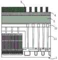
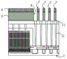
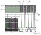
1、目标结构;11、半导体器件层;2、反应腔;3、低介电材料层;4、保护层;5、掩膜层;6、导电槽;7隔离结构;8、金属导线。1. Target structure; 11. Semiconductor device layer; 2. Reaction cavity; 3. Low dielectric material layer; 4. Protective layer; 5. Mask layer; 6. Conductive groove; 7. Isolation structure; 8. Metal wire.
具体实施方式Detailed ways
为使本公开实施例的目的、技术方案和优点更加清楚,下面将结合本公开实施例中的附图,对公开实施例中的技术方案进行清楚、完整地描述,显然,所描述的实施例是本公开一部分实施例,而不是全部的实施例。基于本公开中的实施例,本领域技术人员在没有做出创造性劳动前提下所获得的所有其他实施例,都属于本公开保护的范围。需要说明的是,在不冲突的情况下,本公开中的实施例及实施例中的特征可以相互任意组合。In order to make the purpose, technical solutions and advantages of the embodiments of the present disclosure clearer, the technical solutions in the disclosed embodiments will be clearly and completely described below in conjunction with the drawings in the embodiments of the present disclosure. Obviously, the described embodiments It is a part of the embodiments of the present disclosure, but not all of them. Based on the embodiments in the present disclosure, all other embodiments obtained by those skilled in the art without making creative efforts belong to the protection scope of the present disclosure. It should be noted that, in the case of no conflict, the embodiments in the present disclosure and the features in the embodiments can be combined arbitrarily with each other.
相关技术中,为了降低金属导线之间的寄生电容,改善寄生电容造成的响应延迟,采用低介电材料层作为金属导线之间的层间介质。降低低介电材料层的介电常数常采用的方式为,在材料中引入甲基(–CH3)。然而,甲基容易受到等离子体的攻击而出现断裂,降低了层间介质的质量,金属导线之间的层间介质的可靠性下降。In the related art, in order to reduce the parasitic capacitance between the metal wires and improve the response delay caused by the parasitic capacitance, a low dielectric material layer is used as the interlayer dielectric between the metal wires. A common way to reduce the dielectric constant of the low-dielectric material layer is to introduce a methyl group (–CH3 ) into the material. However, the methyl group is easily attacked by the plasma and breaks, which reduces the quality of the interlayer dielectric and reduces the reliability of the interlayer dielectric between the metal wires.
图10示出了一个对比实施例示出的刻蚀后的低介电材料层的透射电子显微镜(TEM)扫描图,参照图10所示,低介电材料层刻蚀后容易出现表面“尖角”的轮廓(参照图10中A区域),“尖角”处缩小了相邻的两根金属之间的距离,导致相邻的两根金属导线在“尖角”处容易发生短路(Bridge)问题。并且,在形成金属导线的制程中,涉及填充金属铜(或者其它金属材料)的步骤,填充金属铜通常采用电镀的方式生长金属铜,由于“尖角”的存在导致低介电材料层的顶部接触角较大,不利于电镀过程金属铜的生长。Fig. 10 shows a transmission electron microscope (TEM) scanning image of the low dielectric material layer after etching shown in a comparative example. " outline (refer to the A area in Figure 10), the "sharp corner" reduces the distance between two adjacent metals, resulting in two adjacent metal wires prone to short circuit (Bridge) at the "sharp corner" question. Moreover, in the process of forming metal wires, the step of filling metal copper (or other metal materials) is involved. The filling metal copper is usually grown by electroplating. Due to the existence of "sharp corners", the top of the low dielectric material layer The contact angle is large, which is not conducive to the growth of metal copper in the electroplating process.
因此,形成低介电材料层之后,通常在低介电材料层的表面生长一层氧化物层(比如氧化硅层),以保护低介电材料层的顶面轮廓,图11示出了一个对比实施例中在低介电材料层上形成氧化物层后再进行刻蚀的透射电子显微镜(TEM)扫描图,比较图10、图11可以看出,在低介电材料层上形成氧化物层能够避免低介电材料层的顶部在刻蚀后出现“尖角”的轮廓(参照图11中的B区域)。相关技术中,低介电材料层和氧化物层在不同的腔室中形成,涉及到半导体结构的转移过程,不仅增加了制程的复杂度,还增加了半导体结构的加工时长。Therefore, after the low dielectric material layer is formed, an oxide layer (such as a silicon oxide layer) is usually grown on the surface of the low dielectric material layer to protect the top surface profile of the low dielectric material layer. FIG. 11 shows a In the comparative example, the transmission electron microscope (TEM) scanning diagram of etching after forming an oxide layer on the low dielectric material layer, comparing Fig. 10 and Fig. 11, it can be seen that the oxide layer is formed on the low dielectric material layer layer can avoid the "sharp" profile of the top of the low-k material layer after etching (refer to area B in Figure 11). In the related art, the low-dielectric material layer and the oxide layer are formed in different chambers, which involves the transfer process of the semiconductor structure, which not only increases the complexity of the manufacturing process, but also increases the processing time of the semiconductor structure.
本公开示例性的实施例提供了一种半导体结构的制作方法及半导体结构,在形成低介电材料层之后,无需将半导体结构转移至另一腔室,而是通过调整反应条件,在低介电材料层的顶面上直接形成保护层,保护层的材料和氧化物具有相似的性质,保护层覆盖在低介电材料层的顶面上,能够保护低介电材料层的顶面轮廓,还能避免刻蚀后在低介电材料层的顶面出现“尖角”的轮廓。同时,本实施例的半导体结构的制作方法节约了转移半导体结构的过程,节约了一个腔室,极大程度的降低了半导体结构的生产成本、提高了制程效率并减少了制程时间(cycle time)。Exemplary embodiments of the present disclosure provide a method for fabricating a semiconductor structure and a semiconductor structure. After forming a low dielectric material layer, it is not necessary to transfer the semiconductor structure to another chamber, but by adjusting the reaction conditions, the A protective layer is directly formed on the top surface of the electrical material layer, the material of the protective layer has similar properties to the oxide, the protective layer covers the top surface of the low dielectric material layer, and can protect the top surface profile of the low dielectric material layer, It can also avoid "sharp" contours appearing on the top surface of the low dielectric material layer after etching. At the same time, the manufacturing method of the semiconductor structure in this embodiment saves the process of transferring the semiconductor structure, saves a chamber, greatly reduces the production cost of the semiconductor structure, improves the process efficiency and reduces the process time (cycle time) .
本公开示例性的实施例中提供一种半导体结构的制作方法,如图1所示,图1示出了根据本公开一示例性的实施例提供的半导体结构的制作方法的流程图,图3-图5为半导体结构的制作方法的各个阶段的示意图,下面结合图3-图5对半导体结构的制作方法进行介绍。An exemplary embodiment of the present disclosure provides a method for manufacturing a semiconductor structure, as shown in FIG. 1 , and FIG. 1 shows a flow chart of a method for manufacturing a semiconductor structure according to an exemplary embodiment of the present disclosure. FIG. 3 - FIG. 5 is a schematic diagram of various stages of the manufacturing method of the semiconductor structure, and the manufacturing method of the semiconductor structure will be introduced below in conjunction with FIGS. 3-5 .
本实施例对半导体结构不作限制,下面将以半导体结构为动态随机存储器(Dynamic Random Access Memory,DRAM)为例进行介绍,但本实施例并不以此为限,本实施例中的半导体结构还可以为其他的结构。This embodiment does not limit the semiconductor structure. The following will introduce the semiconductor structure as Dynamic Random Access Memory (DRAM) as an example, but this embodiment is not limited thereto. The semiconductor structure in this embodiment is also Other configurations are possible.
如图1所示,本公开一示例性的实施例提供的一种半导体结构的制作方法,包括如下的步骤:As shown in FIG. 1 , a method for fabricating a semiconductor structure provided by an exemplary embodiment of the present disclosure includes the following steps:
步骤S110:将目标结构置于反应腔中,向反应腔中通入第一反应气体和第二反应气体。Step S110: placing the target structure in the reaction chamber, and introducing the first reaction gas and the second reaction gas into the reaction chamber.
如图3所示,目标结构1可以包括晶圆,其中,晶圆为半导体晶圆,例如可以为硅(Si)晶圆、锗(Ge)晶圆、锗硅(SiGe)晶圆、绝缘体上硅(Silicon On Insulator,SOI)晶圆或绝缘体上锗(Germanium On Insulator,GOI)晶圆等。半导体晶圆还可以为包括其它元素半导体或化合物半导体的晶圆,例如砷化镓(GaAs)、磷化铟(InP)或碳化硅(SiC)等,半导体晶圆还可以为叠层结构,例如半导体晶圆为硅晶圆-锗硅晶圆形成的叠层结构。As shown in FIG. 3 , the target structure 1 may include a wafer, wherein the wafer is a semiconductor wafer, such as a silicon (Si) wafer, a germanium (Ge) wafer, a silicon germanium (SiGe) wafer, or an on-insulator wafer. Silicon (Silicon On Insulator, SOI) wafer or Germanium On Insulator (Germanium On Insulator, GOI) wafer, etc. The semiconductor wafer can also be a wafer including other elemental semiconductors or compound semiconductors, such as gallium arsenide (GaAs), indium phosphide (InP) or silicon carbide (SiC), etc. The semiconductor wafer can also be a stacked structure, such as The semiconductor wafer is a stacked structure formed of a silicon wafer-germanium silicon wafer.
目标结构1还可以包括其它外延结构,例如绝缘体上锗硅(Silicon Germanium OnInsulater,SGOI)等。The target structure 1 may also include other epitaxial structures, such as Silicon Germanium On Insulator (SGOI) and the like.
目标结构1还可以包括一层或多层堆叠的半导体器件层,半导体器件层可以形成在晶圆中或设置在晶圆上。其中,每层半导体器件层中可以设置多种半导体器件和多种金属互连结构。其中,半导体器件可以包括金属氧化物半导体场效应晶体管、双极结晶体管、电阻器、电感器、二极管、光学器件中的至少一种。The target structure 1 may also include one or more stacked semiconductor device layers, and the semiconductor device layers may be formed in the wafer or provided on the wafer. Wherein, various semiconductor devices and various metal interconnection structures can be arranged in each semiconductor device layer. Wherein, the semiconductor device may include at least one of a metal oxide semiconductor field effect transistor, a bipolar junction transistor, a resistor, an inductor, a diode, and an optical device.
如图3所示,将目标结构1置于反应腔2中后,抽出反应腔2中的空气,反应腔2中形成真空状态。接着,向反应腔2中通入载气,通过调节载气的流量速率等参数调整反应腔2内的压强,使反应腔2内处于低压状态。在本实施例中,低压状态是指反应腔2内的压力低于10Torr。其中,载气选用惰性气体,例如,载气可以选择氦气。As shown in FIG. 3 , after the target structure 1 is placed in the
然后,向反应腔2中通入第一反应气体和第二反应气体,可以将第一反应气体和第二反应气体分别通入到反应腔2中;也可以将第一反应气体和第二反应气体在反应腔2外按比例混合后再将混合气体通入到反应腔2中。向反应腔2中通入混合气体的同时,可以采用冷却装置冷却用于输送混合气体的气体通路,避免第一反应气体和第二反应气体在气体通路中反应。Then, feed the first reaction gas and the second reaction gas into the
在反应腔中,通过等离子体增强的化学气相沉积法(Plasma Enhanced ChemicalVapor Deposition,PECVD)处理第一反应气体和第二反应气体,在目标结构1上沉积形成介电材料层3(后续步骤中会进行详细说明)和保护层4(后续步骤中会进行详细说明),第一反应气体可以为硅源气体,第二反应气体可以为氧源气体。In the reaction chamber, the first reaction gas and the second reaction gas are processed by plasma-enhanced chemical vapor deposition (Plasma Enhanced Chemical Vapor Deposition, PECVD), and a
步骤S120:将反应腔内的工艺条件调节为第一工艺条件,第一反应气体和第二反应气体在目标结构上形成低介电材料层。Step S120: Adjust the process conditions in the reaction chamber to the first process conditions, and the first reaction gas and the second reaction gas form a low-dielectric material layer on the target structure.
参照图3,在第一工艺条件下,第一反应气体、第二反应气体反应沉积,在目标结构1上生长低介电材料,生长结束后,如图4所示,在目标结构1上形成低介电材料层3。Referring to FIG. 3 , under the first process condition, the first reaction gas and the second reaction gas are reactively deposited to grow a low dielectric material on the target structure 1. After the growth is completed, as shown in FIG. 4 , a low dielectric material is formed on the target structure 1. Low
低介电材料层3的厚度根据工艺需求设置,并根据低介电材料层3的厚度控制第一反应气体和第二反应气体在目标结构1上生长低介电材料的时长。The thickness of the low
本实施例形成的低介电材料层3的材料包括硅元素和氧元素,低介电材料层3的材料的介电常数小于3。The material of the low
步骤S130:将第一工艺条件调节为第二工艺条件,第一反应气体和第二反应气体在低介电材料层上形成保护层。Step S130: adjusting the first process condition to the second process condition, the first reaction gas and the second reaction gas form a protective layer on the low dielectric material layer.
参照图3,低介电材料层3生长结束后,继续向反应腔2中通入载气、第一反应气体和第二反应气体,同时调节反应腔2内的工艺条件,将第一工艺条件调节为第二工艺条件,第二工艺条件和第一工艺条件不同。可以理解的是,将第一工艺条件调节为第二工艺条件的同时,可以调节第一反应气体的流量速率和第二反应气体的流量速率,从而调节向反应腔2中通入第一反应气体和第二反应气体的流量比。Referring to Fig. 3, after the growth of the low-
在反应腔2中,第一反应气体和第二反应气体在第二工艺条件下反应沉积,如图5所示,在低介电材料层3的顶面生长保护层4。保护层4的材料的组分和低介电材料层3的材料组分类似,均包括硅元素和氧元素。但保护层4的材料的性质和低介电材料层3的材料的性质不同,保护层4的性质和氧化物(比如氧化硅)类似。保护层4覆盖在低介电材料层3的顶面上,能够避免后续刻蚀过程中低介电材料层3发生损伤,同时,保护层4能够避免刻蚀低介电材料层3时在低介电材料层3的顶面形成“尖角”的轮廓。In the
本实施例的半导体结构的制作方法,优化了低介电材料层的制程工艺,在反应腔中形成低介电材料层后,调节反应腔中的工艺条件,在低介电材料层上原位生长形成保护层,保护层保护低介电材料层的顶面轮廓,避免刻蚀在低介电材料的顶面形成“尖角”的轮廓;本实施例的半导体结构的制作方法,无需转移目标结构,即可在同一反应腔中形成低介电材料层和保护层,节省了在低介电材料层上沉积形成氧化物层的步骤,节省了在低介电材料层上沉积氧化物层的腔室,提高了制程效率、减少了制程时间,降低了生产成本。The manufacturing method of the semiconductor structure in this embodiment optimizes the process technology of the low dielectric material layer. After the low dielectric material layer is formed in the reaction chamber, the process conditions in the reaction chamber are adjusted, and the low dielectric material layer is in situ Growth to form a protective layer, the protective layer protects the top surface profile of the low dielectric material layer, and avoids etching to form a "sharp corner" profile on the top surface of the low dielectric material; the manufacturing method of the semiconductor structure in this embodiment does not need to transfer the target structure, the low dielectric material layer and the protective layer can be formed in the same reaction chamber, which saves the step of depositing and forming the oxide layer on the low dielectric material layer, and saves the time of depositing the oxide layer on the low dielectric material layer The chamber improves the process efficiency, reduces the process time and reduces the production cost.
根据一个示例性实施例,本实施例是对上述实施例的说明,在本实施例中,第一反应气体包括至少一种环状有机硅氧烷,第二反应气体包括至少一种含氧气体。According to an exemplary embodiment, which is an illustration of the above embodiment, in this embodiment, the first reactive gas comprises at least one cyclic organosiloxane and the second reactive gas comprises at least one oxygen-containing gas .
环状有机硅氧烷包括具有一个或者多个硅-碳键的化合物。可以采用具有一个或者多个环的环状有机硅氧烷化合物,每个环具有交替的硅和氧原子,且每个环具有键合到硅原子上的一个或者多个烷基。Cyclic organosiloxanes include compounds having one or more silicon-carbon bonds. Cyclic organosiloxane compounds having one or more rings, each ring having alternating silicon and oxygen atoms, and each ring having one or more alkyl groups bonded to the silicon atoms may be employed.
示例性的,环状有机硅氧烷可以选自以下化合物中的至少一种:1,3,5,7-四甲基环四硅氧烷(TMCTS),-(-SiHCH3-O-)4-(环状)、八甲基环四硅氧烷(OMCTS),-(-Si(CH3)2-O-)4-(环状)、1,3,5,7,9-五甲基环五硅氧烷,-(-SiHCH3-O-)5-(环状)、六甲基环三硅氧烷,-(-Si(CH3)2-O-)3-(环状)、十甲基环五硅氧烷,-(-Si(CH3)2-O-)5-(环状)。可以理解的是,至少一种环状有机硅氧烷的选择并不限制于此示例。Exemplary, the cyclic organosiloxane can be selected from at least one of the following compounds: 1,3,5,7-tetramethylcyclotetrasiloxane (TMCTS), -(-SiHCH3-O-)4 -(cyclic), octamethylcyclotetrasiloxane (OMCTS), -(-Si(CH3)2-O-)4-(cyclic), 1,3,5,7,9-pentamethyl Cyclopentasiloxane, -(-SiHCH3-O-)5-(cyclic), hexamethylcyclotrisiloxane, -(-Si(CH3)2-O-)3-(cyclic), deca Methylcyclopentasiloxane, -(-Si(CH3)2-O-)5-(cyclic). It is understood that the selection of at least one cyclic organosiloxane is not limited to this example.
含氧气体可以采用任意合适的含分子氧的气体的形式提供,例如,可以直接提供分子氧,比如氧气或臭氧;或提供空气。The oxygen-containing gas may be provided in the form of any suitable molecular oxygen-containing gas, for example, molecular oxygen such as oxygen or ozone may be provided directly; or air may be provided.
参照图5,第一反应气体和第二反应在第一工艺条件下生长的低介电材料层3的材料包括硅氧碳材料。低介电材料层3的材料中包括甲基(–CH3),能够进一步降低介电材料层3的介电常数。Referring to FIG. 5 , the material of the low
第一反应气体和第二反应在第二工艺条件下生长的保护层的材料包括掺杂碳的硅氧材料。保护层4的材料的氧含量高于低介电材料层3的材料的氧含量,且保护层4的材料的碳含量小于低介电材料层3的材料的碳含量。The material of the protective layer grown under the second process condition by the first reaction gas and the second reaction includes carbon-doped silicon-oxygen material. The oxygen content of the material of the
本实施例以至少一种环状有机硅氧烷以及至少一种含氧气体为气体源,至少一种环状有机硅氧烷和至少一种含氧气体在第一工艺条件下形成低介电材料层,低介电材料层的介电常数更低,低介电材料层作为层间介质能够进一步降低半导体器件之间的耦合电容,提高半导体结构的响应速度,有利于半导体结构的特征尺寸进一步减小;至少一种环状有机硅氧烷和至少一种含氧气体在第二工艺条件下形成保护层,保护层覆盖低介电材料层的顶面,既能保护低介电材料层的顶面轮廓,还能避免刻蚀低介电材料层的制程中,在低介电材料层的顶面形成“尖角”的轮廓。In this embodiment, at least one cyclic organosiloxane and at least one oxygen-containing gas are used as gas sources, and at least one cyclic organosiloxane and at least one oxygen-containing gas form a low-dielectric material layer, the dielectric constant of the low-dielectric material layer is lower, and the low-dielectric material layer as an interlayer medium can further reduce the coupling capacitance between semiconductor devices, improve the response speed of the semiconductor structure, and facilitate the further improvement of the characteristic size of the semiconductor structure. Reduce; at least one cyclic organosiloxane and at least one oxygen-containing gas form a protective layer under the second process conditions, and the protective layer covers the top surface of the low dielectric material layer, which can protect the low dielectric material layer The top surface profile can also avoid the formation of a "sharp corner" profile on the top surface of the low dielectric material layer during the process of etching the low dielectric material layer.
本公开示例性的实施例中提供一种半导体结构的制作方法,如图2所示,图2示出了根据本公开一示例性的实施例提供的半导体结构的制作方法的流程图,图3-图8为半导体结构的制作方法的各个阶段的示意图,下面结合图3-图8对半导体结构的制作方法进行介绍。An exemplary embodiment of the present disclosure provides a method for manufacturing a semiconductor structure, as shown in FIG. 2 . FIG. 2 shows a flowchart of a method for manufacturing a semiconductor structure according to an exemplary embodiment of the present disclosure. FIG. 3 - FIG. 8 is a schematic diagram of various stages of the manufacturing method of the semiconductor structure, and the manufacturing method of the semiconductor structure will be introduced below in conjunction with FIGS. 3-8 .
如图2所示,本公开一示例性的实施例提供的一种半导体结构的制作方法,包括如下的步骤:As shown in FIG. 2, a method for fabricating a semiconductor structure provided by an exemplary embodiment of the present disclosure includes the following steps:
步骤S210:将目标结构置于反应腔中,向反应腔中通入第一反应气体和第二反应气体。Step S210: placing the target structure in the reaction chamber, and introducing the first reaction gas and the second reaction gas into the reaction chamber.
如图3所示,首先,提供目标结构1,目标结构1为晶圆,目标结构1中设置有半导体器件层11,每层半导体器件层11中设置有多个半导体器件。本实施例中的晶圆、半导体器件层11和上述实施例中的晶圆、半导体器件层11相同,在此不再赘述。As shown in FIG. 3 , firstly, a target structure 1 is provided. The target structure 1 is a wafer, and semiconductor device layers 11 are disposed in the target structure 1 , and multiple semiconductor devices are disposed in each
然后,将目标结构1转移到反应腔2中,并将反应腔2抽至真空状态。本实施例中,反应腔2为低压化学气相沉积腔室。Then, the target structure 1 is transferred into the
接着,向反应腔2中分别通入第一反应气体和第二反应气体,第一反应气体包括至少一种环状有机硅氧烷,第二反应气体包括至少一种含氧气体。在本实施例中,至少一种环状有机硅氧烷包括八甲基环四硅氧烷,至少一种含氧气体包括氧气。Next, a first reaction gas and a second reaction gas are introduced into the
步骤S220:将反应腔内的工艺条件调节为第一工艺条件,第一反应气体和第二反应气体在目标结构上形成低介电材料层。Step S220: Adjust the process conditions in the reaction chamber to the first process conditions, and the first reaction gas and the second reaction gas form a low-dielectric material layer on the target structure.
参照图3,将反应腔2内的工艺条件调节为第一工艺条件,包括:Referring to Fig. 3, the process condition in the
首先,将反应腔2内温度调整至350℃-400℃。First, adjust the temperature in the
然后,以第一流量速率向反应腔2中通入第一反应气体,以第二流量速率向反应腔2中通入第二反应气体。Then, the first reaction gas is introduced into the
第一流量速率为2500sccm~3500sccm。例如,第一流量速率可以为2500sccm、2700sccm、2900sccm、3000sccm、3100sccm、3300sccm或3500sccm。The first flow rate is from 2500 sccm to 3500 sccm. For example, the first flow rate may be 2500 seem, 2700 seem, 2900 seem, 3000 seem, 3100 seem, 3300 seem, or 3500 seem.
第二流量速率为120sccm~180sccm。例如,第二流量速率可以为120sccm、130sccm、140sccm、150sccm、160sccm、170sccm或180sccm。The second flow rate is from 120 sccm to 180 sccm. For example, the second flow rate may be 120 seem, 130 seem, 140 seem, 150 seem, 160 seem, 170 seem, or 180 seem.
然后,开启射频源,使射频源输出第一射频功率,向反应腔2中通入惰性气体,控制惰性气体的流量速率为第五流量速率,并将反应腔2内的压力调节为第一压力,第一反应气体和第二反应气体发生第一化学反应,第一化学反应的反应产物沉积在目标结构1上形成低介电材料层3。Then, turn on the radio frequency source, make the radio frequency source output the first radio frequency power, feed the inert gas in the
射频源为脉冲射频源,射频源脉冲输出第一射频功率;或者,射频源为连续波射频源,射频源连续输出第一射频功率。The radio frequency source is a pulsed radio frequency source, and the radio frequency source pulses to output the first radio frequency power; or, the radio frequency source is a continuous wave radio frequency source, and the radio frequency source continuously outputs the first radio frequency power.
在本实施例中,射频源包括高频射频源和低频射频源,高频射频源和低频射频源均为脉冲射频源,高频射频源的射频功率为540W~660W,低频射频源的射频功率为低频45W~55W,高频,第一射频功率的高频功率和低频功率的相位差能够改善沉积形成的低介电材料层3的均匀性,以使形成的低介电材料层3的厚度均匀一致,避免出现在目标结构1的中心区域形成的低介电材料层3的厚度大于目标结构1的边缘区域的低介电材料层3的厚度等问题,进一步提高了低介电材料层3的质量。In this embodiment, the radio frequency source includes a high frequency radio frequency source and a low frequency radio frequency source, both of which are pulsed radio frequency sources, the radio frequency power of the high frequency radio frequency source is 540W~660W, and the radio frequency power of the low frequency radio frequency source is Low frequency 45W~55W, high frequency, the phase difference between the high frequency power and low frequency power of the first radio frequency power can improve the uniformity of the low
向反应腔2中通入惰性气体,惰性气体为后续形成低介电材料层3和保护层4(后续步骤会进行详细说明)提供惰性氛围。在本实施例中,惰性气体包括氦气,第五流量速率为2200sccm~2800sccm。An inert gas is introduced into the
同时,通过调节惰性气体的第五流量速率将反应腔2中的压力调节至第一压力,第一压力为4Torr~6Torr。例如,可以将反应腔2中的压力调节至4Torr、4.3Torr、4.5Torr、4.8Torr、5Torr、5.3Torr、5.7Torr或6Torr。可以理解的是,在第一反应气体和第二反应气体发生第一化学反应的过程中,反应腔2中的压力可以是波动的或变化的,在反应腔2中的压力发生波动或变化时,实时调节惰性气体的第五流量速率将反应腔2中的压力维持在第一压力的范围中即可,并不局限于将反应腔2中的压力维持在某一压力值。At the same time, the pressure in the
第一反应气体、第二反应气体和惰性气体在第一工艺条件下通过等离子体增强化学的气相沉积法形成低介电材料,第一射频功率引导低介电材料的移动方向,以使低介电材料生长在目标结构1的表面,形成低介电材料层3,能够促进低介电材料沉积、加快低介电材料层3的形成。The first reaction gas, the second reaction gas and the inert gas form the low dielectric material through plasma enhanced chemical vapor deposition method under the first process condition, and the first radio frequency power guides the moving direction of the low dielectric material, so that the low dielectric material The electrical material grows on the surface of the target structure 1 to form the low
第一反应气体和第二反应气体在目标结构1的顶面上形成的低介电材料层3的材料包括硅氧碳材料,低介电材料层3的介电常数小于3。比如,低介电材料层3的材料包括碳氧化硅(SiOC)。The material of the low
步骤S230:将第一工艺条件调节为第二工艺条件,第一反应气体和第二反应气体在低介电材料层上形成保护层。Step S230: Adjust the first process condition to the second process condition, and the first reaction gas and the second reaction gas form a protective layer on the low dielectric material layer.
在本实施例中,将第一工艺条件调节为第二工艺条件,可以采用以下实施方式:In this embodiment, the first process condition is adjusted to the second process condition, the following implementation manners can be adopted:
参照图4,保持反应腔2内的温度为350℃-400℃不变,将射频源的输出功率调节为第二射频功率,将惰性气体的流量速率调节为第六流量速率,并将反应腔2内的压力调节为第二压力;同时,将第一反应气体由第一流量速率调节为第三流量速率,将第二反应气体由第二流量速率调节为第四流量速率。Referring to Figure 4, keep the temperature in the
通过调节射频源,使射频源从输出第一射频功率转为输出第二射频功率,第二射频功率为低频80W~100W,高频300W~500W。调节射频源输出的射频功率的同时,调节惰性气体的流量速率至第六流量速率,第六流量速率为1500sccm~2000sccm,将反应腔2中的压力调节由第一压力调节至第二压力,第二压力为7Torr~8Torr。例如,可以将反应腔2中的压力调节至7Torr、7.2Torr、7.4Torr、7.5Torr、7.6Torr、7.8Torr、7.9Torr或8Torr。可以理解的是,在第一反应气体和第二反应气体发生第二化学反应的过程中,实时调节惰性气体的流量速率以使反应腔2中的压力维持在第二压力的范围中。By adjusting the radio frequency source, the radio frequency source is changed from outputting the first radio frequency power to outputting the second radio frequency power. The second radio frequency power is 80W~100W for low frequency and 300W~500W for high frequency. While adjusting the radio frequency power output by the radio frequency source, adjust the flow rate of the inert gas to the sixth flow rate, the sixth flow rate is 1500sccm~2000sccm, and adjust the pressure in the
第一反应气体由第一流量速率调节为第三流量速率,将第二反应气体由第二流量速率调节为第四流量速率,能够降低向反应腔2中通入的第一反应气体的流量速率,增加向反应腔2中通入的第二反应气体的流量速率,从而降低反应腔2中八甲基环四硅氧烷的含量,增加反应腔2中氧气的含量,以使第一反应气体和第二反应气体发生第二化学反应的反应产物具有更高的氧含量。The first reaction gas is adjusted from the first flow rate to the third flow rate, and the second reaction gas is adjusted from the second flow rate to the fourth flow rate, which can reduce the flow rate of the first reaction gas passed into the
第三流量速率为400sccm-500sccm;第四流量速率为200sccm~500sccm。示例性的,第三流量速率可以为400sccm、420sccm、450sccm、460sccm、470sccm、480sccm或500sccm;第四流量速率可以为200sccm、250sccm、300sccm、350sccm、400sccm、450sccm或500sccm。The third flow rate is 400sccm-500sccm; the fourth flow rate is 200sccm-500sccm. Exemplarily, the third flow rate may be 400 sccm, 420 sccm, 450 sccm, 460 sccm, 470 sccm, 480 sccm or 500 sccm; the fourth flow rate may be 200 sccm, 250 sccm, 300 sccm, 350 sccm, 400 sccm, 450 sccm or 500 sccm.
如图5所示,在第二工艺条件下,第一反应气体和第二反应气体发生第二化学反应,第二化学反应的反应产物沉积在低介电材料层3上形成保护层4。保护层4的材料主要包括掺杂碳的硅氧材料。本实施例中,保护层4的材料包括碳氧化硅(SiOC)复合材料,保护层的材料中氧元素的含量高于低介电材料层的材料中氧元素的含量;保护层的材料中碳元素的含量低于低介电材料层的材料中碳元素的含量。本实施例形成的保护层4的材料性质和氧化硅的性质类似,且保护层4的材料的介电常数比氧化硅的介电常数低。As shown in FIG. 5 , under the second process condition, the first reaction gas and the second reaction gas undergo a second chemical reaction, and the reaction product of the second chemical reaction is deposited on the low
在一些实施例中,为了提高形成的保护层4的材料的氧含量,以使保护层4的性质更加接近氧化硅,进一步提高保护层4对低介电材料层3的顶面轮廓的保护效果,在形成保护层4的过程中,增加反应腔2中第二反应气体的占比。比如,可以将第一反应气体和第二反应气体的流量比设置为1,或者,将第一反应气体和第二反应气体的流量比设置为小于1。In some embodiments, in order to increase the oxygen content of the material of the formed
在一些实施例中,将反应腔2维持在第二工艺条件下预设时长,在低介电材料层2上形成第一厚度的保护层4,第一厚度为30nm~50nm。示例性的,第一厚度可以为30nm、35nm、40nm、45nm或50nm。In some embodiments, the
保护层4的厚度为30nm~50nm时,保护层4覆盖低介电材料层3的顶面,足以避免低介电材料层3在后续的工艺制程中被损伤。比如,图案化低介电材料层3的制程中,通常采用刻蚀工艺刻蚀低介电材料层3,保护层4的厚度为30nm~50nm即可为低介电材料层3提高充足的防护,避免被保护层4覆盖的低介电材料层3被过度刻蚀,避免在低介电材料层3的顶面形成“尖角”的轮廓,从而提高图案化低介电材料层3的精确度以及制程的可控性,避免“尖角”的轮廓对半导体结构产生的不良影响,提高半导体结构的可靠性。同时,保护层4的厚度在此范围内,能够避免保护层4的厚度太厚,影响低介电材料层3降低耦合电容的效果,以使半导体结构具有更快的响应速度。When the thickness of the
本实施例的半导体结构的制作方法,在低介电材料层上形成的保护层的性质更接近氧化硅,保护层替代氧化物保护低介电材料层的效果更好;并且,保护层的材料的介电常数比氧化硅的介电常数低,保护层能够更好的降低半导体结构中器件间的耦合电容。In the manufacturing method of the semiconductor structure of this embodiment, the property of the protective layer formed on the low dielectric material layer is closer to that of silicon oxide, and the effect of the protective layer replacing the oxide to protect the low dielectric material layer is better; and, the material of the protective layer The dielectric constant of silicon oxide is lower than that of silicon oxide, and the protective layer can better reduce the coupling capacitance between devices in the semiconductor structure.
根据一个示例性实施例,本实施例包括上述实施例的全部步骤,本实施例和上述实施例的区别之处在于,在步骤S230之后,还包括以下步骤:According to an exemplary embodiment, this embodiment includes all the steps of the above embodiments, and the difference between this embodiment and the above embodiments is that after step S230, the following steps are further included:
步骤S240:刻蚀保护层和低介电材料层,形成多个导线槽。Step S240: Etching the protection layer and the low dielectric material layer to form a plurality of wire grooves.
如图6所示,在保护层4的顶面上形成掩膜层5,掩膜层5暴露出保护层4的部分顶面,基于掩膜层5依次刻蚀保护层4和低介电材料层3,去除被掩膜层5暴露出的保护层4和低介电材料层3,如图7所示,形成多个独立设置的导线槽6,导线槽6暴露出目标结构1的顶面。多个导电槽6将保护层4和低介电材料层3划分成多个隔离结构7,隔离结构7设置在相邻的两个导线槽6之间,每个隔离结构7包括位于目标结构1上的低介电材料层3以及覆盖低介电材料层3的顶面的保护层4。其中,刻蚀工艺可以选用干法工艺或湿法工艺。As shown in Figure 6, a
形成多个导线槽6的过程中,先去除被掩膜层5暴露出的保护层4,暴露出低介电材料层3的部分顶面,然后,刻蚀被保护层4暴露出的低介电材料层3。刻蚀低介电材料层3的过程中,保护层4发挥良好的掩蔽效果,避免被其覆盖的低介电材料层3被刻蚀工艺去除或损伤,以将刻蚀低介电材料层3的范围限制在被保护层4暴露出的区域,以使形成的导线槽6的形貌和特征尺寸更符合预期。如图7所示,在垂直于目标结构1的顶面的截面,导线槽6划分出的每个隔离结构7的宽度上下一致,被保留的低介电材料层3的顶部没有“尖角”等轮廓缺陷,隔离结构7具有良好的隔离效果。In the process of forming a plurality of
步骤S250:于导线槽中形成金属导线。Step S250 : forming metal wires in the wire groove.
如图8所示,参照图7,沉积金属导电材料填充导电槽6,在每个导电槽6中形成一个金属导线8,相邻的金属导线8被隔离结构7隔开。As shown in FIG. 8 , referring to FIG. 7 , conductive metal material is deposited to fill the
如图8所示,在垂直于目标结构1的顶面的截面,每个隔离结构7的宽度上下一致(即图8中示出的竖向方向),具有良好的隔离效果。由于低介电材料层3的介电常数低于3,能够有效降低相邻的金属导线8之间的耦合电容。同时,保护层4具有比氧化物更低的介电常数,能够进一步降低相邻的两个金属导线8的顶部间的耦合电容,进一步改善半导体结构的响应延迟的问题,提高半导体结构的响应数量,从而提高半导体结构的性能和可靠性。As shown in FIG. 8 , in a section perpendicular to the top surface of the target structure 1 , the width of each isolation structure 7 is consistent from top to bottom (that is, the vertical direction shown in FIG. 8 ), which has a good isolation effect. Since the dielectric constant of the low
下面列出本示例性实施例的具体实施例:The specific examples of this exemplary embodiment are listed below:
表1示出了本示例性实施例中半导体结构的制作方法中形成的低介电材料层的具体参数,表2示出了本示例性实施例中半导体结构的制作方法中形成的低介电材料层的具体参数。需要指出的是,本公开的半导体结构的制作方法的具体参数并不局限于表1、表2中的数据。Table 1 shows the specific parameters of the low dielectric material layer formed in the manufacturing method of the semiconductor structure in this exemplary embodiment, and Table 2 shows the low dielectric material layer formed in the manufacturing method of the semiconductor structure in this exemplary embodiment. The specific parameters of the material layer. It should be pointed out that the specific parameters of the manufacturing method of the semiconductor structure of the present disclosure are not limited to the data in Table 1 and Table 2.
表1 形成低介电材料层的具体实施例Table 1 Specific examples of forming a low dielectric material layer

表2 形成保护层的具体实施例Table 2 forms the specific embodiment of protective layer

其中,OMCTS为八甲基环四硅氧烷。Wherein, OMCTS is octamethylcyclotetrasiloxane.
检测以上实施例的半导体结构的制作方法制作的半导体结构,低介电材料层和保护层的各组分含量如表3所示,在本实施例中,低介电材料层和保护层的各组分含量以质量百分比计。Detecting the semiconductor structure produced by the method for manufacturing the semiconductor structure in the above embodiment, the contents of each component of the low dielectric material layer and the protective layer are shown in Table 3. In this embodiment, the components of the low dielectric material layer and the protective layer are Component content is calculated by mass percentage.
表3 半导体结构的材料的组分表Table 3 Composition list of materials for semiconductor structures

按照以上实施例的半导体结构的制作方法,制作实施例1-5的半导体结构,并检测实施例1-5的半导体结构的保护层的性能。在低介电材料层上沉积形成氧化物层,制作对比实施例1-5的半导体结构,并检测对比实施例1-5的半导体结构的氧化物层的性能,性能检测结果如表4所示。According to the manufacturing method of the semiconductor structure of the above embodiments, the semiconductor structures of Examples 1-5 were fabricated, and the performance of the protective layer of the semiconductor structures of Examples 1-5 was tested. Deposit and form an oxide layer on the low dielectric material layer, make the semiconductor structure of Comparative Examples 1-5, and detect the performance of the oxide layer of the semiconductor structure of Comparative Examples 1-5, and the performance test results are shown in Table 4. .
表4 实施例1-5的保护层以及对比实施例1-5的氧化物层的性能检测结果Table 4 Performance testing results of the protective layer of Examples 1-5 and the oxide layer of Comparative Examples 1-5

根据表4记录的性能检测结果的数据可知,实施例1-5的半导体结构中的保护层的的性能检测结果和对比实施例1-5中氧化物层的性能检测结构接近,采用保护层替代氧化物层没有明显缺陷,保护层能够替代氧化物层保护低介电材料层,并实现良好的替代效果。According to the data of the performance test results recorded in Table 4, it can be seen that the performance test results of the protective layer in the semiconductor structure of Examples 1-5 are close to the performance test structure of the oxide layer in Comparative Examples 1-5, and the protective layer is used instead. The oxide layer has no obvious defects, and the protection layer can replace the oxide layer to protect the low dielectric material layer, and achieve a good replacement effect.
对本实施例形成的半导体结构进行刻蚀处理后,对本实施例形成的半导体结构进行透射电子显微镜扫描,扫描结构如图9所示,参照图9所示,本实施例形成的半导体结构,保护层4覆盖在低介电材料层3上,刻蚀后低介电材料层3的顶面没有出现“尖角”的轮廓(参照图9中C区域),半导体结构的顶面轮廓良好,本实施例通过在低介电材料层3上形成保护层4替代氧化物层,同样能够实现保护低介电材料层3的顶面轮廓的效果,避免半导体结构中刻蚀形成的沟槽的顶面的间距缩小的问题,从而避免在沟槽中形成的导电结构短路,从而提高半导体结构的良率和电性能。After the semiconductor structure formed in this embodiment is etched, the semiconductor structure formed in this embodiment is scanned by a transmission electron microscope. The scanning structure is shown in Figure 9. Referring to Figure 9, the semiconductor structure formed in this embodiment, the
根据一示例性实施例提供了一种半导体结构,如图5、图6、图7或图8所示,半导体结构包括目标结构1、设置在目标结构1上的低介电材料层3以及设置在低介电材料层3上的保护层4,低介电材料层3与保护层4由相同的前驱体制备,保护层4具有更低的碳含量。其中,低介电材料层3的材料的介电常数小于3。According to an exemplary embodiment, a semiconductor structure is provided. As shown in FIG. 5, FIG. 6, FIG. 7 or FIG. The
在一些实施例中,低介电材料层3的材料包括硅氧碳材料。保护层4的材料包括硅氧碳材料。In some embodiments, the material of the low
保护层4的材料和低介电材料层3的材料的成分类似,但保护层4中的氧含量大于低介电材料层3中的氧含量,保护层4中的碳含量小于低介电材料层3中的碳含量,保护层4的性质和低介电材料层3性质不同。保护层4的性质更接近氧化物,保护层3设置在低介电材料层3上具有良好的掩蔽效果,改善并保护低介电材料层3的顶面轮廓,以使低介电材料层3可以作为层间介质设置在半导体器件之间,降低半导体器件之间的耦合电容,提高半导体结构的响应速度,提高半导体结构的良率和可靠性。The composition of the material of the
在一些实施例中,前驱体包括至少一种环状有机硅氧烷。In some embodiments, the precursor includes at least one cyclic organosiloxane.
在一些实施例中,至少一种环状有机硅氧烷包括八甲基环四硅氧烷。In some embodiments, the at least one cyclic organosiloxane includes octamethylcyclotetrasiloxane.
在一些实施例中,低介电材料层的材料包括硅氧碳材料,保护层的材料包括掺杂碳的硅氧材料。In some embodiments, the material of the low dielectric material layer includes a silicon-oxygen-carbon material, and the material of the protection layer includes a carbon-doped silicon-oxygen material.
在一些实施例中,保护层的碳含量小于5%。In some embodiments, the carbon content of the protective layer is less than 5%.
在一些实施例中,保护层的碳含量小于2%。In some embodiments, the protective layer has a carbon content of less than 2%.
在一些实施例中,低介电材料的碳含量大于10%。In some embodiments, the carbon content of the low dielectric material is greater than 10%.
在一些实施例中,低介电材料的碳含量介于10%到30%之间。In some embodiments, the carbon content of the low-k material is between 10% and 30%.
在一些实施例中,保护层具有第一厚度,第一厚度为30nm~50nm。示例性的,第一厚度可以为30nm、35nm、40nm、45nm或50nm。保护层4的厚度在此范围内足以为低介电材料层3提高良好的防护,改善并保护低介电材料层的顶面轮廓;同时,保护层4的厚度在此范围内,能够避免保护层4的厚度太厚,影响低介电材料层3降低耦合电容的效果,半导体结构具有更快的响应速度。In some embodiments, the protective layer has a first thickness, and the first thickness is 30 nm˜50 nm. Exemplarily, the first thickness may be 30nm, 35nm, 40nm, 45nm or 50nm. The thickness of the
本实施例的半导体结构可以为存储芯片,存储芯片可以用在动态随机存储器(Dynamic Random Access Memory,DRAM)中。然而,也可以应用于静态随机存取存储器(Static Random-Access Memory,SRAM)、快闪存储器(flash EPROM)、铁电存储器(Ferroelectric Random-Access Memory,FRAM)、磁性随机存取存储器(Magnetic Random-Access Memory,MRAM)、相变随机存储器(Phase change Random-Access Memory,PRAM)等。The semiconductor structure in this embodiment may be a memory chip, and the memory chip may be used in a dynamic random access memory (Dynamic Random Access Memory, DRAM). However, it can also be applied to static random access memory (Static Random-Access Memory, SRAM), flash memory (flash EPROM), ferroelectric memory (Ferroelectric Random-Access Memory, FRAM), magnetic random access memory (Magnetic Random -Access Memory, MRAM), phase change random access memory (Phase change Random-Access Memory, PRAM), etc.
本说明书中各实施例或实施方式采用递进的方式描述,每个实施例重点说明的都是与其他实施例的不同之处,各个实施例之间相同相似部分相互参见即可。Each embodiment or implementation manner in this specification is described in a progressive manner, each embodiment focuses on the differences from other embodiments, and the same and similar parts of each embodiment can be referred to each other.
在本说明书的描述中,参考术语“实施例”、“示例性的实施例”、“一些实施方式”、“示意性实施方式”、“示例”等的描述意指结合实施方式或示例描述的具体特征、结构、材料或者特点包含于本公开的至少一个实施方式或示例中。In the description of this specification, descriptions with reference to the terms "embodiments", "exemplary embodiments", "some implementations", "exemplary implementations", "examples" and the like mean that the descriptions are described in conjunction with the implementations or examples. A specific feature, structure, material, or characteristic is included in at least one embodiment or example of the present disclosure.
在本说明书中,对上述术语的示意性表述不一定指的是相同的实施方式或示例。而且,描述的具体特征、结构、材料或者特点可以在任何的一个或多个实施方式或示例中以合适的方式结合。In this specification, schematic representations of the above terms do not necessarily refer to the same embodiment or example. Furthermore, the described specific features, structures, materials or characteristics may be combined in any suitable manner in any one or more embodiments or examples.
在本公开的描述中,需要说明的是,术语“中心”、“上”、“下”、“左”、“右”、“竖直”、“水平”、“内”、“外”等指示的方位或位置关系为基于附图所示的方位或位置关系,仅是为了便于描述本公开和简化描述,而不是指示或暗示所指的装置或元件必须具有特定的方位、以特定的方位构造和操作,因此不能理解为对本公开的限制。In the description of the present disclosure, it should be noted that the terms "center", "upper", "lower", "left", "right", "vertical", "horizontal", "inner", "outer" etc. The indicated orientation or positional relationship is based on the orientation or positional relationship shown in the drawings, and is only for the convenience of describing the present disclosure and simplifying the description, rather than indicating or implying that the referred device or element must have a specific orientation, or in a specific orientation. construction and operation are therefore not to be construed as limitations on the present disclosure.
可以理解的是,本公开所使用的术语“第一”、“第二”等可在本公开中用于描述各种结构,但这些结构不受这些术语的限制。这些术语仅用于将第一个结构与另一个结构区分。It can be understood that the terms "first", "second" and the like used in the present disclosure can be used to describe various structures in the present disclosure, but these structures are not limited by these terms. These terms are only used to distinguish one structure from another.
在一个或多个附图中,相同的元件采用类似的附图标记来表示。为了清楚起见,附图中的多个部分没有按比例绘制。此外,可能未示出某些公知的部分。为了简明起见,可以在一幅图中描述经过数个步骤后获得的结构。在下文中描述了本公开的许多特定的细节,例如器件的结构、材料、尺寸、处理工艺和技术,以便更清楚地理解本公开。但正如本领域技术人员能够理解的那样,可以不按照这些特定的细节来实现本公开。In one or more drawings, like elements are indicated with like reference numerals. For the sake of clarity, various parts in the drawings are not drawn to scale. Also, some well-known parts may not be shown. For simplicity, the structure obtained after several steps can be described in one figure. In the following, many specific details of the present disclosure, such as structures, materials, dimensions, processing techniques and techniques of devices, are described for a clearer understanding of the present disclosure. However, as will be understood by those skilled in the art, the present disclosure may be practiced without these specific details.
最后应说明的是:以上各实施例仅用以说明本公开的技术方案,而非对其限制;尽管参照前述各实施例对本公开进行了详细的说明,本领域技术人员应当理解:其依然可以对前述各实施例所记载的技术方案进行修改,或者对其中部分或者全部技术特征进行等同替换;而这些修改或者替换,并不使相应技术方案的本质脱离本公开各实施例技术方案的范围。Finally, it should be noted that: the above embodiments are only used to illustrate the technical solutions of the present disclosure, not to limit them; although the present disclosure has been described in detail with reference to the foregoing embodiments, those skilled in the art should understand that: it can still Modifications are made to the technical solutions described in the foregoing embodiments, or equivalent replacements are made to some or all of the technical features; these modifications or replacements do not make the essence of the corresponding technical solutions depart from the scope of the technical solutions of the embodiments of the present disclosure.
Claims (21)
Translated fromChinesePriority Applications (3)
| Application Number | Priority Date | Filing Date | Title |
|---|---|---|---|
| CN202310104747.0ACN115775768B (en) | 2023-02-13 | 2023-02-13 | Semiconductor structure and manufacturing method thereof |
| PCT/CN2023/126732WO2024169230A1 (en) | 2023-02-13 | 2023-10-26 | Semiconductor structure and fabrication method therefor |
| US18/822,469US20240429042A1 (en) | 2023-02-13 | 2024-09-03 | Semiconductor structure and method for manufacturing same |
Applications Claiming Priority (1)
| Application Number | Priority Date | Filing Date | Title |
|---|---|---|---|
| CN202310104747.0ACN115775768B (en) | 2023-02-13 | 2023-02-13 | Semiconductor structure and manufacturing method thereof |
Publications (2)
| Publication Number | Publication Date |
|---|---|
| CN115775768A CN115775768A (en) | 2023-03-10 |
| CN115775768Btrue CN115775768B (en) | 2023-07-04 |
Family
ID=85393684
Family Applications (1)
| Application Number | Title | Priority Date | Filing Date |
|---|---|---|---|
| CN202310104747.0AActiveCN115775768B (en) | 2023-02-13 | 2023-02-13 | Semiconductor structure and manufacturing method thereof |
Country Status (3)
| Country | Link |
|---|---|
| US (1) | US20240429042A1 (en) |
| CN (1) | CN115775768B (en) |
| WO (1) | WO2024169230A1 (en) |
Families Citing this family (1)
| Publication number | Priority date | Publication date | Assignee | Title |
|---|---|---|---|---|
| CN115775768B (en)* | 2023-02-13 | 2023-07-04 | 长鑫存储技术有限公司 | Semiconductor structure and manufacturing method thereof |
Citations (1)
| Publication number | Priority date | Publication date | Assignee | Title |
|---|---|---|---|---|
| CN112331554A (en)* | 2019-08-05 | 2021-02-05 | 长鑫存储技术有限公司 | Thin film deposition method, semiconductor device manufacturing method and semiconductor device |
Family Cites Families (18)
| Publication number | Priority date | Publication date | Assignee | Title |
|---|---|---|---|---|
| US6340435B1 (en)* | 1998-02-11 | 2002-01-22 | Applied Materials, Inc. | Integrated low K dielectrics and etch stops |
| JP4068072B2 (en)* | 2003-01-29 | 2008-03-26 | Necエレクトロニクス株式会社 | Semiconductor device and manufacturing method thereof |
| JP4086673B2 (en)* | 2003-02-04 | 2008-05-14 | Necエレクトロニクス株式会社 | Semiconductor device and manufacturing method thereof |
| JP3778174B2 (en)* | 2003-04-14 | 2006-05-24 | ソニー株式会社 | Semiconductor device and manufacturing method thereof |
| US7271093B2 (en)* | 2004-05-24 | 2007-09-18 | Asm Japan K.K. | Low-carbon-doped silicon oxide film and damascene structure using same |
| US7273823B2 (en)* | 2005-06-03 | 2007-09-25 | Applied Materials, Inc. | Situ oxide cap layer development |
| JP2007258208A (en)* | 2006-03-20 | 2007-10-04 | Sumitomo Bakelite Co Ltd | Semiconductor device |
| US7431859B2 (en)* | 2006-04-28 | 2008-10-07 | Applied Materials, Inc. | Plasma etch process using polymerizing etch gases with different etch and polymer-deposition rates in different radial gas injection zones with time modulation |
| JP2009004633A (en)* | 2007-06-22 | 2009-01-08 | Fujitsu Microelectronics Ltd | Multilayer wiring structure and manufacturing method |
| JP2010171081A (en)* | 2009-01-20 | 2010-08-05 | Toshiba Corp | Semiconductor device and manufacturing method thereof |
| CN101937863B (en)* | 2009-07-03 | 2012-01-25 | 中芯国际集成电路制造(上海)有限公司 | Method for making metal wiring |
| CN102403261B (en)* | 2010-09-09 | 2013-09-11 | 中芯国际集成电路制造(上海)有限公司 | Semiconductor device and manufacturing method thereof |
| US10297442B2 (en)* | 2013-05-31 | 2019-05-21 | Lam Research Corporation | Remote plasma based deposition of graded or multi-layered silicon carbide film |
| CN105097657B (en)* | 2014-05-09 | 2018-06-29 | 中芯国际集成电路制造(上海)有限公司 | The forming method of semiconductor structure |
| CN105990105B (en)* | 2015-01-27 | 2019-01-08 | 中芯国际集成电路制造(上海)有限公司 | The production method of hard mask layer, the production method of interlayer dielectric layer and semiconductor devices |
| US11749563B2 (en)* | 2018-06-27 | 2023-09-05 | Taiwan Semiconductor Manufacturing Co., Ltd. | Interlayer dielectric layer |
| CN115775768B (en)* | 2023-02-13 | 2023-07-04 | 长鑫存储技术有限公司 | Semiconductor structure and manufacturing method thereof |
| CN116779587A (en)* | 2023-08-02 | 2023-09-19 | 长鑫科技集团股份有限公司 | Semiconductor structure and preparation method thereof |
- 2023
- 2023-02-13CNCN202310104747.0Apatent/CN115775768B/enactiveActive
- 2023-10-26WOPCT/CN2023/126732patent/WO2024169230A1/enactivePending
- 2024
- 2024-09-03USUS18/822,469patent/US20240429042A1/enactivePending
Patent Citations (1)
| Publication number | Priority date | Publication date | Assignee | Title |
|---|---|---|---|---|
| CN112331554A (en)* | 2019-08-05 | 2021-02-05 | 长鑫存储技术有限公司 | Thin film deposition method, semiconductor device manufacturing method and semiconductor device |
Also Published As
| Publication number | Publication date |
|---|---|
| CN115775768A (en) | 2023-03-10 |
| WO2024169230A1 (en) | 2024-08-22 |
| US20240429042A1 (en) | 2024-12-26 |
Similar Documents
| Publication | Publication Date | Title |
|---|---|---|
| TWI706512B (en) | Ic structure with interface liner and methods of forming same | |
| KR100925310B1 (en) | Method of forming thin sgoi wafers with high relaxation and low stacking fault defect density | |
| JP4731670B2 (en) | Low-K dielectric composite layer for integrated circuit structures providing void-free low-k dielectric material between metal lines while mitigating via poisoning | |
| TWI798794B (en) | Method for fabricating semiconductor device | |
| US9831098B2 (en) | Methods for fabricating integrated circuits using flowable chemical vapor deposition techniques with low-temperature thermal annealing | |
| KR101327640B1 (en) | Method for forming a dielectric film and novel precursors for implementing said method | |
| CN105097644A (en) | Methods for producing integrated circuits with an insulating layer | |
| TWI803361B (en) | Semiconductor device with composite word line structure and method for fabricating the same | |
| CN104752504A (en) | Semiconductor Device Structure And Method For Manufacturing The Same | |
| CN115775768B (en) | Semiconductor structure and manufacturing method thereof | |
| TWI817380B (en) | Semiconductor device having integral alignment marks with decoupling features and method for fabricating the same | |
| WO2021178478A1 (en) | Low temperature steam free oxide gapfill | |
| TWI885677B (en) | Method for fabricating semiconductor device with filling layer | |
| CN101996921B (en) | STI forming method | |
| CN117612995A (en) | Substrate processing method | |
| CN117790546A (en) | Semiconductor element with peripheral gate structure and preparation method thereof | |
| CN115172261A (en) | Method for manufacturing SOI epitaxial silicon | |
| US20070161208A1 (en) | Semiconductor device and fabrication method thereof | |
| CN111933688A (en) | Semiconductor structure and preparation method thereof | |
| TWI841514B (en) | Method for fabricating semiconductor device with assistance features | |
| CN113838858B (en) | Method for preparing three-dimensional memory | |
| US20230098689A1 (en) | Deposition of boron nitride films using hydrazido-based precursors | |
| CN110896050A (en) | Method for forming dielectric film | |
| US20230111315A1 (en) | Method for fabricating semiconductor device with plug structure | |
| KR20240114626A (en) | An amorphous boron nitride film, semiconductor device and field effect transistor including the same, and method of manufacturing the carbon atom doped amorphous boron nitride film |
Legal Events
| Date | Code | Title | Description |
|---|---|---|---|
| PB01 | Publication | ||
| PB01 | Publication | ||
| SE01 | Entry into force of request for substantive examination | ||
| SE01 | Entry into force of request for substantive examination | ||
| GR01 | Patent grant | ||
| GR01 | Patent grant |