CN115775716A - Substrate support assembly and plasma processing apparatus - Google Patents
Substrate support assembly and plasma processing apparatusDownload PDFInfo
- Publication number
- CN115775716A CN115775716ACN202211052630.4ACN202211052630ACN115775716ACN 115775716 ACN115775716 ACN 115775716ACN 202211052630 ACN202211052630 ACN 202211052630ACN 115775716 ACN115775716 ACN 115775716A
- Authority
- CN
- China
- Prior art keywords
- substrate support
- electrode plate
- support assembly
- susceptor
- substrate
- Prior art date
- Legal status (The legal status is an assumption and is not a legal conclusion. Google has not performed a legal analysis and makes no representation as to the accuracy of the status listed.)
- Pending
Links
- 239000000758substrateSubstances0.000titleclaimsabstractdescription138
- 238000012545processingMethods0.000titleclaimsabstractdescription91
- 238000012546transferMethods0.000claimsabstractdescription25
- 238000010438heat treatmentMethods0.000claimsabstractdescription6
- 229910052751metalInorganic materials0.000claimsdescription22
- 239000002184metalSubstances0.000claimsdescription22
- 239000000463materialSubstances0.000claimsdescription17
- 239000011148porous materialSubstances0.000claimsdescription13
- 238000009413insulationMethods0.000claimsdescription10
- RTAQQCXQSZGOHL-UHFFFAOYSA-NTitaniumChemical compound[Ti]RTAQQCXQSZGOHL-UHFFFAOYSA-N0.000claimsdescription9
- 239000010936titaniumSubstances0.000claimsdescription9
- 229910052719titaniumInorganic materials0.000claimsdescription9
- MCMNRKCIXSYSNV-UHFFFAOYSA-NZirconium dioxideChemical compoundO=[Zr]=OMCMNRKCIXSYSNV-UHFFFAOYSA-N0.000claimsdescription8
- 238000007789sealingMethods0.000claimsdescription7
- 229910052782aluminiumInorganic materials0.000claimsdescription6
- XAGFODPZIPBFFR-UHFFFAOYSA-NaluminiumChemical compound[Al]XAGFODPZIPBFFR-UHFFFAOYSA-N0.000claimsdescription6
- PNEYBMLMFCGWSK-UHFFFAOYSA-Naluminium oxideInorganic materials[O-2].[O-2].[O-2].[Al+3].[Al+3]PNEYBMLMFCGWSK-UHFFFAOYSA-N0.000claimsdescription6
- 229920006169PerfluoroelastomerPolymers0.000claimsdescription3
- 239000004642PolyimideSubstances0.000claimsdescription3
- 239000011248coating agentSubstances0.000claimsdescription3
- 238000000576coating methodMethods0.000claimsdescription3
- 229920001721polyimidePolymers0.000claimsdescription3
- 229920002449FKMPolymers0.000claimsdescription2
- 239000002241glass-ceramicSubstances0.000claimsdescription2
- 229920001296polysiloxanePolymers0.000claimsdescription2
- 239000010935stainless steelSubstances0.000claimsdescription2
- 229910001220stainless steelInorganic materials0.000claimsdescription2
- 229910000601superalloyInorganic materials0.000claimsdescription2
- GWEVSGVZZGPLCZ-UHFFFAOYSA-NTitan oxideChemical compoundO=[Ti]=OGWEVSGVZZGPLCZ-UHFFFAOYSA-N0.000claims2
- RUDFQVOCFDJEEF-UHFFFAOYSA-Nyttrium(III) oxideInorganic materials[O-2].[O-2].[O-2].[Y+3].[Y+3]RUDFQVOCFDJEEF-UHFFFAOYSA-N0.000claims1
- 239000007789gasSubstances0.000description52
- 238000001179sorption measurementMethods0.000description18
- 239000000919ceramicSubstances0.000description13
- 230000004048modificationEffects0.000description12
- 238000012986modificationMethods0.000description12
- 230000002093peripheral effectEffects0.000description12
- 238000010586diagramMethods0.000description11
- 239000010410layerSubstances0.000description11
- 238000000034methodMethods0.000description10
- 230000000694effectsEffects0.000description7
- 238000009832plasma treatmentMethods0.000description5
- 230000006837decompressionEffects0.000description4
- 239000013013elastic materialSubstances0.000description4
- 239000012212insulatorSubstances0.000description4
- 230000001105regulatory effectEffects0.000description4
- 239000004065semiconductorSubstances0.000description4
- 238000004891communicationMethods0.000description3
- 238000001816coolingMethods0.000description3
- 238000009792diffusion processMethods0.000description3
- 238000005530etchingMethods0.000description3
- 238000009616inductively coupled plasmaMethods0.000description3
- 150000002500ionsChemical class0.000description3
- 230000008569processEffects0.000description3
- 239000003507refrigerantSubstances0.000description3
- 238000003860storageMethods0.000description3
- BSYNRYMUTXBXSQ-UHFFFAOYSA-NAspirinChemical compoundCC(=O)OC1=CC=CC=C1C(O)=OBSYNRYMUTXBXSQ-UHFFFAOYSA-N0.000description2
- 230000008901benefitEffects0.000description2
- 230000015572biosynthetic processEffects0.000description2
- 229920001971elastomerPolymers0.000description2
- 238000005516engineering processMethods0.000description2
- 238000004519manufacturing processMethods0.000description2
- 239000002861polymer materialSubstances0.000description2
- 239000007787solidSubstances0.000description2
- 238000004381surface treatmentMethods0.000description2
- BQCIDUSAKPWEOX-UHFFFAOYSA-N1,1-DifluoroetheneChemical compoundFC(F)=CBQCIDUSAKPWEOX-UHFFFAOYSA-N0.000description1
- 229910000838Al alloyInorganic materials0.000description1
- 229910000505Al2TiO5Inorganic materials0.000description1
- BOTDANWDWHJENH-UHFFFAOYSA-NTetraethyl orthosilicateChemical compoundCCO[Si](OCC)(OCC)OCCBOTDANWDWHJENH-UHFFFAOYSA-N0.000description1
- 229910001069Ti alloyInorganic materials0.000description1
- 229910000883Ti6Al4VInorganic materials0.000description1
- IWBUYGUPYWKAMK-UHFFFAOYSA-N[AlH3].[N]Chemical compound[AlH3].[N]IWBUYGUPYWKAMK-UHFFFAOYSA-N0.000description1
- 230000002159abnormal effectEffects0.000description1
- 230000009471actionEffects0.000description1
- 238000005513bias potentialMethods0.000description1
- 238000010288cold sprayingMethods0.000description1
- 230000006835compressionEffects0.000description1
- 238000007906compressionMethods0.000description1
- 238000010276constructionMethods0.000description1
- PMHQVHHXPFUNSP-UHFFFAOYSA-Mcopper(1+);methylsulfanylmethane;bromideChemical compoundBr[Cu].CSCPMHQVHHXPFUNSP-UHFFFAOYSA-M0.000description1
- 230000006866deteriorationEffects0.000description1
- 238000007598dipping methodMethods0.000description1
- 238000007599dischargingMethods0.000description1
- 229920001973fluoroelastomerPolymers0.000description1
- 230000006870functionEffects0.000description1
- 239000001307heliumSubstances0.000description1
- 229910052734heliumInorganic materials0.000description1
- SWQJXJOGLNCZEY-UHFFFAOYSA-Nhelium atomChemical compound[He]SWQJXJOGLNCZEY-UHFFFAOYSA-N0.000description1
- 238000007731hot pressingMethods0.000description1
- 150000005828hydrofluoroalkanesChemical class0.000description1
- 238000002347injectionMethods0.000description1
- 239000007924injectionSubstances0.000description1
- 238000005304joiningMethods0.000description1
- 239000007788liquidSubstances0.000description1
- 239000007769metal materialSubstances0.000description1
- 229910044991metal oxideInorganic materials0.000description1
- 150000004706metal oxidesChemical class0.000description1
- TWNQGVIAIRXVLR-UHFFFAOYSA-Noxo(oxoalumanyloxy)alumaneChemical compoundO=[Al]O[Al]=OTWNQGVIAIRXVLR-UHFFFAOYSA-N0.000description1
- SIWVEOZUMHYXCS-UHFFFAOYSA-Noxo(oxoyttriooxy)yttriumChemical compoundO=[Y]O[Y]=OSIWVEOZUMHYXCS-UHFFFAOYSA-N0.000description1
- 239000002245particleSubstances0.000description1
- 239000000843powderSubstances0.000description1
- 238000003672processing methodMethods0.000description1
- AABBHSMFGKYLKE-SNAWJCMRSA-Npropan-2-yl (e)-but-2-enoateChemical compoundC\C=C\C(=O)OC(C)CAABBHSMFGKYLKE-SNAWJCMRSA-N0.000description1
- 239000011347resinSubstances0.000description1
- 229920005989resinPolymers0.000description1
- 239000003566sealing materialSubstances0.000description1
- HBMJWWWQQXIZIP-UHFFFAOYSA-Nsilicon carbideChemical compound[Si+]#[C-]HBMJWWWQQXIZIP-UHFFFAOYSA-N0.000description1
- 229910010271silicon carbideInorganic materials0.000description1
- 239000002356single layerSubstances0.000description1
- 238000005507sprayingMethods0.000description1
- 238000009834vaporizationMethods0.000description1
- 230000008016vaporizationEffects0.000description1
- 238000003466weldingMethods0.000description1
Images


Classifications
- H—ELECTRICITY
- H01—ELECTRIC ELEMENTS
- H01J—ELECTRIC DISCHARGE TUBES OR DISCHARGE LAMPS
- H01J37/00—Discharge tubes with provision for introducing objects or material to be exposed to the discharge, e.g. for the purpose of examination or processing thereof
- H01J37/32—Gas-filled discharge tubes
- H01J37/32431—Constructional details of the reactor
- H01J37/32715—Workpiece holder
- H01J37/32724—Temperature
- H—ELECTRICITY
- H01—ELECTRIC ELEMENTS
- H01L—SEMICONDUCTOR DEVICES NOT COVERED BY CLASS H10
- H01L21/00—Processes or apparatus adapted for the manufacture or treatment of semiconductor or solid state devices or of parts thereof
- H01L21/67—Apparatus specially adapted for handling semiconductor or electric solid state devices during manufacture or treatment thereof; Apparatus specially adapted for handling wafers during manufacture or treatment of semiconductor or electric solid state devices or components ; Apparatus not specifically provided for elsewhere
- H01L21/67005—Apparatus not specifically provided for elsewhere
- H01L21/67011—Apparatus for manufacture or treatment
- H01L21/67017—Apparatus for fluid treatment
- H01L21/67063—Apparatus for fluid treatment for etching
- H01L21/67069—Apparatus for fluid treatment for etching for drying etching
- H—ELECTRICITY
- H01—ELECTRIC ELEMENTS
- H01L—SEMICONDUCTOR DEVICES NOT COVERED BY CLASS H10
- H01L21/00—Processes or apparatus adapted for the manufacture or treatment of semiconductor or solid state devices or of parts thereof
- H01L21/67—Apparatus specially adapted for handling semiconductor or electric solid state devices during manufacture or treatment thereof; Apparatus specially adapted for handling wafers during manufacture or treatment of semiconductor or electric solid state devices or components ; Apparatus not specifically provided for elsewhere
- H01L21/67005—Apparatus not specifically provided for elsewhere
- H01L21/67011—Apparatus for manufacture or treatment
- H01L21/67098—Apparatus for thermal treatment
- H01L21/67103—Apparatus for thermal treatment mainly by conduction
- H—ELECTRICITY
- H01—ELECTRIC ELEMENTS
- H01L—SEMICONDUCTOR DEVICES NOT COVERED BY CLASS H10
- H01L21/00—Processes or apparatus adapted for the manufacture or treatment of semiconductor or solid state devices or of parts thereof
- H01L21/67—Apparatus specially adapted for handling semiconductor or electric solid state devices during manufacture or treatment thereof; Apparatus specially adapted for handling wafers during manufacture or treatment of semiconductor or electric solid state devices or components ; Apparatus not specifically provided for elsewhere
- H01L21/67005—Apparatus not specifically provided for elsewhere
- H01L21/67011—Apparatus for manufacture or treatment
- H01L21/67098—Apparatus for thermal treatment
- H01L21/67109—Apparatus for thermal treatment mainly by convection
- H—ELECTRICITY
- H01—ELECTRIC ELEMENTS
- H01L—SEMICONDUCTOR DEVICES NOT COVERED BY CLASS H10
- H01L21/00—Processes or apparatus adapted for the manufacture or treatment of semiconductor or solid state devices or of parts thereof
- H01L21/67—Apparatus specially adapted for handling semiconductor or electric solid state devices during manufacture or treatment thereof; Apparatus specially adapted for handling wafers during manufacture or treatment of semiconductor or electric solid state devices or components ; Apparatus not specifically provided for elsewhere
- H01L21/683—Apparatus specially adapted for handling semiconductor or electric solid state devices during manufacture or treatment thereof; Apparatus specially adapted for handling wafers during manufacture or treatment of semiconductor or electric solid state devices or components ; Apparatus not specifically provided for elsewhere for supporting or gripping
- H01L21/6831—Apparatus specially adapted for handling semiconductor or electric solid state devices during manufacture or treatment thereof; Apparatus specially adapted for handling wafers during manufacture or treatment of semiconductor or electric solid state devices or components ; Apparatus not specifically provided for elsewhere for supporting or gripping using electrostatic chucks
- H01L21/6833—Details of electrostatic chucks
- H—ELECTRICITY
- H01—ELECTRIC ELEMENTS
- H01J—ELECTRIC DISCHARGE TUBES OR DISCHARGE LAMPS
- H01J2237/00—Discharge tubes exposing object to beam, e.g. for analysis treatment, etching, imaging
- H01J2237/20—Positioning, supporting, modifying or maintaining the physical state of objects being observed or treated
- H01J2237/2007—Holding mechanisms
- H—ELECTRICITY
- H01—ELECTRIC ELEMENTS
- H01J—ELECTRIC DISCHARGE TUBES OR DISCHARGE LAMPS
- H01J2237/00—Discharge tubes exposing object to beam, e.g. for analysis treatment, etching, imaging
- H01J2237/32—Processing objects by plasma generation
- H01J2237/33—Processing objects by plasma generation characterised by the type of processing
- H01J2237/334—Etching
Landscapes
- Engineering & Computer Science (AREA)
- Physics & Mathematics (AREA)
- Microelectronics & Electronic Packaging (AREA)
- General Physics & Mathematics (AREA)
- Manufacturing & Machinery (AREA)
- Computer Hardware Design (AREA)
- Condensed Matter Physics & Semiconductors (AREA)
- Power Engineering (AREA)
- Plasma & Fusion (AREA)
- Chemical & Material Sciences (AREA)
- Analytical Chemistry (AREA)
- Container, Conveyance, Adherence, Positioning, Of Wafer (AREA)
- Chemical Vapour Deposition (AREA)
- Drying Of Semiconductors (AREA)
Abstract
Description
Translated fromChinese技术领域technical field
本发明涉及基片支承体组件和等离子体处理装置。The present invention relates to a substrate support assembly and a plasma processing apparatus.
背景技术Background technique
专利文献1公开了通过使规定的处理气体(原料气体)在处理容器内反应而在被处理体的表面进行成膜的成膜装置。在该成膜装置中设置有:用于在成膜时载置被处理体(例如半导体晶片)的载置台主体(基片支承体);和用于支承载置台主体的基座。载置台主体包括用于调节被处理体的温度的加热单元(加热器),基座在内部具有冷却单元(制冷剂通路)。另外,在该成膜装置中,在载置台与基座之间设置有隔热件。Patent Document 1 discloses a film forming apparatus for forming a film on the surface of an object to be processed by reacting a predetermined processing gas (source gas) in a processing container. This film forming apparatus is provided with: a stage main body (substrate support body) for placing an object to be processed (for example, a semiconductor wafer) during film formation; and a base for supporting the stage main body. The stage main body includes a heating unit (heater) for adjusting the temperature of the object to be processed, and the susceptor has a cooling unit (refrigerant passage) inside. In addition, in this film forming apparatus, a heat insulator is provided between the mounting table and the susceptor.
现有技术文献prior art literature
专利文献patent documents
专利文献1:日本特开2011-192661号公报Patent Document 1: Japanese Patent Laid-Open No. 2011-192661
发明内容Contents of the invention
发明要解决的技术问题The technical problem to be solved by the invention
本发明的技术能够在支承基片的基片支承体组件中提高高温区域中的温度控制性。The technique of the present invention can improve temperature controllability in a high-temperature region in a substrate support assembly that supports a substrate.
用于解决技术问题的手段Means used to solve technical problems
本发明的一个方式是一种基片支承体组件,其特征在于,包括:基座,在该基座中形成有温度调节介质用的流路;用于支承基片的基片支承体,其具有设置在所述基座上的电极板和设置在所述电极板上的静电卡盘;用于对所述基片进行加热的加热器;设置在所述基座与所述电极板之间的弹性部件,其能够使所述基片支承体与所述基座隔开间隔,并且与所述基座和所述电极板一起形成用于向所述基座与所述电极板之间供给传热气体的传热空间;紧固部件,其能够以在所述基座与所述电极板之间夹持有所述弹性部件的状态将所述基座和所述电极板紧固;和隔热部,其能够抑制所述基座与所述电极板之间的经由所述弹性部件的传热。One aspect of the present invention is a substrate support assembly comprising: a base in which a flow path for a temperature regulating medium is formed; a substrate support for supporting a substrate, which It has an electrode plate arranged on the base and an electrostatic chuck arranged on the electrode plate; a heater for heating the substrate; arranged between the base and the electrode plate an elastic member capable of spacing the substrate support from the base, and is formed together with the base and the electrode plate for feeding between the base and the electrode plate a heat transfer space for heat transfer gas; a fastening member capable of fastening the base and the electrode plate with the elastic member sandwiched between the base and the electrode plate; and A heat insulating portion capable of suppressing heat transfer between the base and the electrode plate via the elastic member.
发明效果Invention effect
采用本发明,能够在支承基片的基片支承体组件中提高高温区域中的温度控制性。According to the present invention, it is possible to improve temperature controllability in a high-temperature region in a substrate support assembly for supporting a substrate.
附图说明Description of drawings
图1是示意性地表示等离子体处理系统的结构的说明图。FIG. 1 is an explanatory diagram schematically showing the configuration of a plasma processing system.
图2是表示等离子体处理装置的结构的概要的纵截面图。FIG. 2 is a longitudinal sectional view showing an outline of the structure of the plasma processing apparatus.
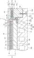
图3是将本实施方式的基片支承体组件的一部分放大表示的说明图。Fig. 3 is an explanatory diagram showing an enlarged part of the substrate support unit according to the present embodiment.
图4是第1变形例的说明图。FIG. 4 is an explanatory diagram of a first modification.
图5是第2变形例的说明图。FIG. 5 is an explanatory diagram of a second modification.
图6是第3变形例的说明图。FIG. 6 is an explanatory diagram of a third modification.
图7是第4变形例的说明图。FIG. 7 is an explanatory diagram of a fourth modification.
图8是第4变形例的说明图。FIG. 8 is an explanatory diagram of a fourth modification.
附图标记说明Explanation of reference signs
1等离子体处理装置,10等离子体处理腔室,10s等离子体处理空间,11基片支承体组件,100基座,101基片支承体,130静电卡盘,131电极板,140吸附用电极,142加热器,160弹性部件,170紧固部件,220隔热部,W基片。1 plasma processing device, 10 plasma processing chamber, 10 s plasma processing space, 11 substrate support assembly, 100 base, 101 substrate support, 130 electrostatic chuck, 131 electrode plate, 140 adsorption electrode, 142 heater, 160 elastic member, 170 fastening member, 220 heat shield, W substrate.
具体实施方式Detailed ways
在半导体器件的制造工序中,对作为被处理体的半导体基片(下面,称为“基片”)进行蚀刻等的等离子体处理。在等离子体处理中,通过使处理气体激发而生成等离子体,利用该等离子体对基片进行处理。In the manufacturing process of a semiconductor device, plasma processing such as etching is performed on a semiconductor substrate (hereinafter, referred to as "substrate") as an object to be processed. In plasma processing, plasma is generated by exciting a processing gas, and a substrate is processed with the plasma.
进行等离子体处理的等离子体处理装置通常包括腔室、基片支承体组件、高频(RF:Radio Frequency)电源。RF电源例如能够向基片支承体组件内的电极(RF电极)供给高频电功率(RF电功率)。在一个例子中,RF电源能够供给:用于生成处理气体的等离子体的源RF电功率(source RF power);和用于将离子引入到基片的偏置RF电功率。基片支承体组件设置在腔室内。基片支承体组件具有RF电极和设置在RF电极上的静电卡盘。A plasma processing apparatus that performs plasma processing generally includes a chamber, a substrate support assembly, and a radio frequency (RF: Radio Frequency) power supply. The RF power supply can supply high-frequency electric power (RF electric power) to electrodes (RF electrodes) in the substrate support assembly, for example. In one example, the RF power supply can supply: source RF power for generating a plasma of the process gas; and bias RF power for introducing ions to the substrate. A substrate support assembly is disposed within the chamber. The substrate support assembly has an RF electrode and an electrostatic chuck disposed on the RF electrode.
然而,近年来,在等离子体处理中,为了应对半导体器件的进一步微细化,研究了BSi、HfO、Ru、WC等难蚀刻掩模材料的应用。为了应对这样的难蚀刻材料,重要的是在高温区域(例如300℃以上)对基片进行等离子体处理。However, in recent years, in order to cope with further miniaturization of semiconductor devices in plasma processing, application of hard-to-etch mask materials such as BSi, HfO, Ru, and WC has been studied. In order to deal with such difficult-to-etch materials, it is important to perform plasma treatment on the substrate in a high-temperature region (for example, above 300° C.).
为了应对高温区域中的等离子体处理,已知有在基片支承体与基座之间夹持密封件,向由它们包围的空间供给氦等传热气体的技术。作为密封件,通常使用橡胶等弹性体制的O形环。然而,弹性体制的O形环,耐热性低,难以应对高温区域中的等离子体处理。因此,考虑使用例如铝、SUS等金属制的O形环或C形环作为密封件。在该情况下,金属的热传导率与橡胶相比非常大,因此,密封件成为热路径,无法高效率地使基片支承体的表面温度上升,有可能导致无法充分地对基片进行加热,或者基片的加热需要高功率。In order to cope with plasma processing in a high-temperature region, there is known a technique in which a seal is interposed between a substrate support and a susceptor, and a heat transfer gas such as helium is supplied to a space surrounded by these. As the seal, an O-ring made of elastic material such as rubber is generally used. However, an elastomeric O-ring has low heat resistance and is difficult to cope with plasma treatment in a high-temperature region. Therefore, it is conceivable to use an O-ring or a C-ring made of metal such as aluminum or SUS as the seal. In this case, the thermal conductivity of metal is very high compared with that of rubber, so the sealing member becomes a heat path, and the surface temperature of the substrate support cannot be raised efficiently, and the substrate may not be sufficiently heated. Or the heating of the substrate requires high power.
本发明的技术是鉴于上述情况而完成的,其能够在对作为被处理体的基片进行等离子体处理等的基片处理装置中,高效率地使基片支承体的表面温度上升,提高高温区域中的温度控制性。下面,参照附图对一个实施方式的等离子体处理系统和包括本实施方式的蚀刻方法的等离子体处理方法进行说明。此外,在本说明书和附图中,对于实质上具有相同的功能结构的要素,通过标注相同的附图标记来省略重复说明。The technology of the present invention was accomplished in view of the above circumstances, and it can efficiently increase the surface temperature of the substrate support in a substrate processing apparatus that performs plasma processing on a substrate as an object to be processed, thereby increasing the Temperature control in the zone. Next, a plasma processing system according to one embodiment and a plasma processing method including the etching method according to this embodiment will be described with reference to the drawings. In addition, in this specification and drawings, the same code|symbol is attached|subjected to the element which has substantially the same functional structure, and repeated description is abbreviate|omitted.
<等离子体处理系统><Plasma processing system>
首先,使用图1对一个实施方式的等离子体处理系统进行说明。图1是示意性地表示等离子体处理系统的结构的说明图。First, a plasma processing system according to one embodiment will be described using FIG. 1 . FIG. 1 is an explanatory diagram schematically showing the configuration of a plasma processing system.
在一个实施方式中,等离子体处理系统包括等离子体处理装置1和控制部2。等离子体处理装置1包括等离子体处理腔室10、基片支承体组件11和等离子体生成部12。等离子体处理腔室10具有等离子体处理空间。另外,等离子体处理腔室10具有:用于向等离子体处理空间供给至少1种处理气体的至少1个气体供给口;和用于从等离子体处理空间排出气体的至少1个气体排出口。气体供给口与后述的气体供给部20连接,气体排出口与后述的排气系统40连接。基片支承体组件11配置在等离子体处理空间内,具有用于支承基片的基片支承面。In one embodiment, a plasma processing system includes a plasma processing apparatus 1 and a control unit 2 . The plasma processing apparatus 1 includes a
等离子体生成部12能够从被供给到等离子体处理空间内的至少1种处理气体生成等离子体。在等离子体处理空间中形成的等离子体可以是电容耦合等离子体(CCP:Capacitively Coupled Plasma)、感应耦合等离子体(ICP:Inductively CoupledPlasma)、ECR等离子体(Electron-Cyclotron-Resonance Plasma:电子回旋共振等离子体)、螺旋波激发等离子体(HWP:Helicon Wave Plasma)、或表面波等离子体(SWP:SurfaceWave Plasma)等。另外,可以使用包括AC(Alternating Current:交流)等离子体生成部和DC(Direct Current:直流)等离子体生成部的各种类型的等离子体生成部。在一个实施方式中,在AC等离子体生成部中使用的AC信号(AC电功率)具有100kHz~10GHz的范围内的频率。因此,AC信号包含RF(Radio Frequency:射频)信号和微波信号。在一个实施方式中,RF信号具有200kHz~150MHz的范围内的频率。The
控制部2能够对计算机可执行的命令进行处理,该命令用于使等离子体处理装置1执行在本发明中说明的各种工序。控制部2能够控制等离子体处理装置1的各要素执行在此说明的各种工序。在一个实施方式中,控制部2的一部分或全部可以包含在等离子体处理装置1中。控制部2例如可以包括计算机2a。计算机2a例如可以包括处理部(CPU:CentralProcessing Unit(中央处理器))2a1、存储部2a2和通信接口2a3。处理部2a1能够基于保存在存储部2a2中的程序来进行各种控制动作。存储部2a2可以包括RAM(Random AccessMemory:随机存取存储器)、ROM(Read Only Memory:只读存储器)、HDD(Hard Disk Drive:硬盘驱动器)、SSD(Solid State Drive:固态驱动器)或者它们的组合。通信接口2a3可以经由LAN(Local Area Network:局域网)等通信线路在与等离子体处理装置1之间进行通信。The control unit 2 can process computer-executable commands for causing the plasma processing apparatus 1 to execute various steps described in the present invention. The control unit 2 can control each element of the plasma processing apparatus 1 to execute various steps described here. In one embodiment, part or all of the control unit 2 may be included in the plasma processing apparatus 1 . The control unit 2 may include, for example, a
<等离子体处理装置><Plasma processing equipment>
下面,使用图2对作为等离子体处理装置1的一个例子的电容耦合等离子体处理装置的结构例进行说明。图2是表示等离子体处理装置1的结构的概要的纵截面图。在本实施方式的等离子体处理装置1中,对基片(晶片)W进行等离子体处理,但是等离子体处理对象的基片W并不限于晶片。Next, a configuration example of a capacitively coupled plasma processing apparatus as an example of the plasma processing apparatus 1 will be described with reference to FIG. 2 . FIG. 2 is a longitudinal sectional view showing an outline of the configuration of the plasma processing apparatus 1 . In the plasma processing apparatus 1 of the present embodiment, the substrate (wafer) W is subjected to plasma processing, but the substrate W to be plasma processed is not limited to the wafer.
电容耦合型的等离子体处理装置1包括等离子体处理腔室10、气体供给部20、电源30和排气系统40。另外,等离子体处理装置1包括基片支承体组件11和气体导入部。气体导入部能够将至少1种处理气体导入到等离子体处理腔室10内。气体导入部包括喷淋头13。基片支承体组件11配置在等离子体处理腔室10内。喷淋头13配置在基片支承体组件11的上方。在一个实施方式中,喷淋头13构成等离子体处理腔室10的顶部(ceiling)的至少一部分。等离子体处理腔室10具有由喷淋头13、等离子体处理腔室10的侧壁10a和基片支承体组件11规定的等离子体处理空间10s。侧壁10a被接地。喷淋头13和基片支承体组件11与等离子体处理腔室10的壳体电绝缘。A capacitively coupled plasma processing apparatus 1 includes a
喷淋头13能够将来自气体供给部20的至少1种处理气体导入到等离子体处理空间10s内。喷淋头13具有至少1个气体供给口13a、至少1个气体扩散室13b和多个气体导入口13c。被供给到气体供给口13a的处理气体,能够通过气体扩散室13b从多个气体导入口13c被导入到等离子体处理空间10s内。另外,喷淋头13包含导电性部件。喷淋头13的导电性部件能够作为上部电极发挥作用。此外,气体导入部可以除了包括喷淋头13以外,还包括被安装于形成在侧壁10a上的1个或多个开口部中的1个或多个侧面气体注入部(SGI:Side GasInjector)。The
气体供给部20可以包括至少1个气体源21和至少1个流量控制器22。在一个实施方式中,气体供给部20能够将至少1种处理气体从与各自对应的气体源21经由与各自对应的流量控制器22供给到喷淋头13。各流量控制器22例如可以包括质量流量控制器或压力控制式的流量控制器。另外,气体供给部20可以包括用于对至少1种处理气体的流量进行调制或脉冲化的至少1个流量调制器件。The
电源30包括经由至少1个阻抗匹配电路与等离子体处理腔室10耦合的RF电源31。RF电源31能够将源RF信号(source RF signal)和偏置RF信号那样的至少1个RF信号(RF电功率)供给到基片支承体组件11的导电性部件和/或喷淋头13的导电性部件。由此,能够从被供给到等离子体处理空间10s的至少1种处理气体形成等离子体。另外,通过向基片支承体组件11的导电性部件供给偏置RF信号,能够在基片W产生偏置电位,将所形成的等离子体中的离子成分引入到基片W。The
在一个实施方式中,RF电源31包括第一RF生成部31a和第二RF生成部31b。第一RF生成部31a经由至少1个阻抗匹配电路与基片支承体组件11的导电性部件和/或喷淋头13的导电性部件耦合,用于生成等离子体生成用的源RF信号(源RF电功率)。在一个实施方式中,源RF信号具有13MHz~150MHz的范围内的频率。在一个实施方式中,可以是第一RF生成部31a能够生成具有不同频率的多个源RF信号。所生成的1个或多个源RF信号被供给到基片支承体组件11的导电性部件和/或喷淋头13的导电性部件。第二RF生成部31b经由至少1个阻抗匹配电路与基片支承体组件11的导电性部件耦合,用于生成偏置RF信号(偏置RF电功率)。在一个实施方式中,偏置RF信号具有比源RF信号的频率低的频率。在一个实施方式中,偏置RF信号具有400kHz~13.56MHz的范围内的频率。在一个实施方式中,可以是第二RF生成部31b能够生成具有不同频率的多个偏置RF信号。所生成的1个或多个偏置RF信号被供给到基片支承体组件11的导电性部件。此外,在各种实施方式中,可以将源RF信号和偏置RF信号中的至少一者进行脉冲化。In one embodiment, the
另外,电源30可以包括与等离子体处理腔室10耦合的DC电源32。DC电源32包括第一DC生成部32a和第二DC生成部32b。在一个实施方式中,第一DC生成部32a与基片支承体组件11的导电性部件连接,用于生成第一DC信号。所生成的第一DC信号被施加于基片支承体组件11的导电性部件。在一个实施方式中,也可以是第一DC信号被施加于静电卡盘内的电极那样的其它电极。在一个实施方式中,第二DC生成部32b与喷淋头13的导电性部件连接,用于生成第二DC信号。所生成的第二DC信号被施加于喷淋头13的导电性部件。在各种实施方式中,可以将第一DC信号和第二DC信号进行脉冲化。此外,可以是除了RF电源31以外还设置第一DC生成部32a和第二DC生成部32b,也可以是设置第一DC生成部32a代替第二RF生成部31b。Additionally,
排气系统40例如能够与设置在等离子体处理腔室10的底部的气体排出口10e连接。排气系统40可以包括压力调节阀和真空泵。能够利用压力调节阀来调节等离子体处理空间10s内的压力。真空泵可以包括涡轮分子泵、干式泵或它们的组合。The
<基片支承体组件><Substrate Support Assembly>
接下来,使用图2和图3对上述的基片支承体组件11和包括该基片支承体组件11的等离子体处理装置1进行说明。图3是将基片支承体组件11的一部分放大表示的说明图。Next, the
用于支承基片W的基片支承体组件11,具有基座100和基片支承体101。基座100被从等离子体处理腔室10的底部延伸的支承部件102支承。该支承部件102是绝缘性的部件,例如由氧化铝(alumina)形成。另外,支承部件102具有大致圆筒形状。The
基座100由具有导电性的金属例如铝形成。基座100具有大致圆盘形状。基座100包括中央部100a和周缘部100b。中央部100a具有大致圆盘形状。中央部100a提供基座100的第1上表面100c。The
周缘部100b在俯视时具有大致圆环形状。周缘部100b与中央部100a相连,在径向上在中央部100a的外侧在周向上延伸。周缘部100b提供基座100的第2上表面100d。第2上表面100d在铅垂方向上位于比第1上表面100c低的位置。另外,周缘部100b与中央部100a一起提供基座100的下表面100e。The
在基座100中形成有温度调节介质用的流路100f。流路100f在基座100内例如呈螺旋状延伸。能够利用设置在等离子体处理腔室10的外部的冷却单元110向该流路100f供给温度调节介质。被供给到流路100f的温度调节介质,在等离子体处理装置1的使用温度范围、例如20℃以上250℃以下的温度区域为液体。或者,温度调节介质可以为能够通过其气化进行吸热来进行冷却的制冷剂,例如可以为氢氟烷类的制冷剂。A
供电体120与基座100连接。供电体120是供电棒,与基座100的下表面100e连接。供电体120由铝或者铝合金形成。供电体120与上述的电源30的RF电源31电连接。The
基片支承体101设置在基座100的第1上表面100c侧。基片支承体101具有静电卡盘130和电极板131。电极板131构成下部电极,设置在基座100之上。电极板131具有导电性。电极板131例如可以为对氮化铝或碳化硅赋予导电性而得到的陶瓷制,或者也可以为金属(例如钛)制。The
电极板131呈大致圆盘形状,具有中央部131a和周缘部131b。中央部131a具有大致圆盘形状。中央部131a提供电极板131的上表面131c。上表面131c为大致圆形的面。周缘部131b与中央部131a相连,在径向上在中央部131a的外侧在周向上延伸。在一个实施方式中,周缘部131b与中央部131a一起提供电极板131的下表面131d。另外,周缘部131b提供上表面131e。该上表面131e为带状的面,在径向上在上表面131c的外侧在周向上延伸。另外,上表面131e在铅垂方向上位于比上表面131c靠近下表面131d的位置。The
静电卡盘130设置在电极板131上,例如通过使用设置在静电卡盘130与电极板131之间的金属形成的金属接合,与电极板131耦合。静电卡盘130具有大致圆盘形状,由陶瓷形成。构成静电卡盘130的陶瓷可以使用在室温(例如20℃)以上400℃以下的温度范围内具有1×10¹⁵Ω·cm以上的体积电阻率的陶瓷。作为这样的陶瓷,例如可以使用作为金属氧化物的氧化铝(alumina)。采用具有这样的体积电阻率的陶瓷制的静电卡盘130,即使在超过200℃的高温区域,也能够发挥充分的吸附力。此外,静电卡盘130也可以使用陶瓷以外的电介质,例如聚酰亚胺。The
静电卡盘130内置有吸附用电极140和加热器142。吸附用电极140是电极膜,该吸附用电极140与直流(DC)电源32电连接。当对吸附用电极140施加来自DC电源32的DC电压时,会产生静电力,能够利用该静电力保持基片W。此外,在本实施方式中,作为静电卡盘例示了库仑型的静电卡盘,但是并不限于此,作为静电卡盘也可以采用约翰逊-拉别克型的静电卡盘。在该情况下,作为构成静电卡盘130的陶瓷,可以使用在室温以上400℃以下的温度范围内具有1×10⁸~1×10¹¹Ω·cm的体积电阻率的陶瓷,例如作为金属氮化物的氮化铝等。The
加热器142设置在吸附用电极140的下方。加热器142例如与装置外的加热器用电源(未图示)电连接。能够对加热器142施加来自加热器电源的电压,将基片W调节为期望的温度。The
在电极板131(基片支承体101)与基座100之间设置有弹性部件的160。弹性部件160与基座100的上表面100c和配置在电极板131的下表面131d侧的隔热部220接触。弹性部件160使基片支承体101在基座100的上方与基座100隔开间隔。该弹性部件160例如是O形环。弹性部件160具有比对传热空间161供给He气时的该传热空间161的热阻高的热阻。另外,弹性部件160要求具有低的热传导率和高的耐热性。这样的弹性部件160可以是弹性体制或金属制。作为弹性体制的弹性部件160,可以由FFKM(全氟弹性体)、FKM(偏氟乙烯类氟橡胶)、硅酮等形成。另外,作为金属制的弹性部件160,可以由铝、SUS、Ni系超合金等形成。An
由基座100、基片支承体101和弹性部件160包围的空间,构成用于供给传热气体的传热空间161。传热空间161在基座100与基片支承体101之间被弹性部件160密封。能够从设置在等离子体处理腔室10的外部的气体供给部(未图示)向传热空间161供给传热气体、例如He气。The space surrounded by the
在电极板131(基片支承体101)与基座100之间,在弹性部件的160的上部设置有隔热部220。隔热部220具有大致环状板形状,是热传导率比电极板131小的部件或空间。即,隔热部220是用于将弹性部件160与电极板131的下表面131d之间热隔断的部件或空间。隔热部220遍及周向地设置在电极板131的下表面131d的周缘131b侧。更具体而言,隔热部件220至少设置于在没有隔热部件220的情况下弹性部件160与下表面131d接触的范围。隔热部220例如可以遍及基座131的中央部131a和周缘部131b地设置在其下表面131d。Between the electrode plate 131 (substrate support 101 ) and the
隔热部220可以由低热传导率的金属、陶瓷、树脂等构成的部件构成。或者,隔热部220可以由形成在规定区域的减压空间构成。在任一情况下,隔热部220的热传导率例如优选为20W/mK以下。当热传导率在这样的范围时,即使在高温区域的基片处理中,即使在使用弹性体制的部件作为弹性部件130的情况下,也能够抑制弹性部件130被加热到耐热温度以上。另外,即使在使用金属制的部件作为弹性部件130的情况下,也能够使经由弹性部件130的热传递量减少,因此,能够高效率地使基片支承体组件的表面温度上升。The
在隔热部220构成为部件的情况下,隔热部220例如可以是低热传导率的含金属材料或陶瓷。作为低热传导率的含金属材料,例如可以例示纯钛、64钛(Ti-6Al-4V)、钛酸铝的含钛材料、不锈钢等。另外,作为陶瓷,可以例示氧化铝、氧化钇、氧化锆、玻璃陶瓷等。另外,隔热部220只要具有300℃以上的耐热性,也可以由高分子材料构成。作为这样的高分子材料,有聚酰亚胺等。If the
另外,在隔热部220构成为部件的情况下,隔热部220可以是实施了表面处理的多孔材料。例如,隔热部220可以为包括多孔材料和覆盖该多孔材料的表面的涂层材料的结构,也可以为具有对表面进行封孔的封孔层的多孔材料。在对多孔材料的表面进行封孔的情况下,封孔层的厚度可以是从多孔材料的表面起为1mm以上,或者也可以是从多孔材料的表面起为2mm以上。作为多孔材料,可以例示多孔氧化铝、多孔钛、多孔氧化锆。作为涂层材料或封孔材料,可以例示铝或钛等金属材料、硅酸乙酯。表面处理例如可以通过冷喷涂或浸渍等来进行。In addition, when the
在隔热部220构成为部件的情况下,隔热部220例如可以通过热压等与基座131一体成型。另外,可以在基座131的下表面131d的外缘设置遍及周向的台阶,通过焊接、喷镀、接合、粘接、螺栓固定等任意的方法将隔热部220安装在该台阶上。隔热部220的位置可以是埋入基座131中那样的配置,或者也可以是安装在基座131的表面(在此为下表面131d)那样的配置。When the
另外,在隔热部220为减压空间的情况下,例如,可以在基座131的下表面131d侧形成遍及周向的空间,通过对该空间进行减压来形成。此外,在作为隔热部220形成减压空间的情况下,可以将减压空间形成为单层结构,也可以形成为多层结构。通过形成为多层结构,能够进一步提高隔热效果。In addition, when the
基片支承体组件11还具有紧固部件170。紧固部件170能够将弹性部件160夹持在基座100与电极板131之间。为了抑制电极板131与基座100之间的来自该紧固部件170的热传导,紧固部件170可以由具有低热传导率的材料例如钛、钛合金等含钛材料形成。The
紧固部件170包括筒状部170a和环状部170b。筒状部170a具有大致圆筒形状,在其下端提供第1下表面170c。环状部170b具有大致环状板形状,与筒状部170a的上侧部分的内缘相连,从该筒状部170a向径向内侧延伸。该环状部170b提供第2下表面170d。The
紧固部件170以第1下表面170c与基座100的上表面100d接触,第2下表面170d与电极板131的上表面131e接触的方式配置。另外,紧固部件170例如可以利用螺钉171被固定在基座100的周缘部100b。在该情况下,能够通过调节螺钉171相对于紧固部件170的紧固力矩,来调节弹性部件160的压扁量(压缩量)。The
此外,可以在紧固部件170的第2下表面170d与电极板131的上表面131e之间设置有弹性部件175。该弹性部件175可以是O形环,能够抑制因第2下表面170d与上述上表面131e的摩擦而可能产生的颗粒(例如,金属粉)移动到等离子体处理空间10s。In addition, an
另外,虽然在此没有图示,但是可以在紧固部件170的第1下表面170c与基座100的上表面100d之间形成具有隔热效果的隔热空间。该隔热空间可以是随着等离子体处理腔室10的抽真空而被减压的结构。In addition, although not shown here, a heat insulating space having a heat insulating effect may be formed between the first
在紧固部件170的上表面侧设置有边缘环180和边缘环用静电卡盘181。另外,在紧固部件170的上表面侧,除了边缘环180和边缘环用静电卡盘181以外还可以设置边缘环温度调节部182。边缘环180、边缘环用静电卡盘181和边缘环温度调节部182从上方向下方去依次层叠。边缘环180以包围被载置在基片支承体101(静电卡盘130)上的基片W的方式配置。边缘环180能够使对基片W的等离子体处理的均匀性提高。An
边缘环用静电卡盘181具有与静电卡盘130同样的结构,即,边缘环用静电卡盘181具有在基层190的内部设置有吸附电极191的结构。基层190在俯视时具有大致圆环形状。基层190可以例如由与静电卡盘130相同的材料形成。另外,基层190可以与吸附保持基片W时的静电力(库仑力或约翰逊-拉别克力)相应地选择。The
吸附电极191是具有导电性的大致圆环形状的电极膜。装置外部的DC电源与吸附电极191电连接。当对吸附电极191施加来自DC电源的DC电压时,边缘环支承体181产生库仑力或约翰逊-拉别克力的静电力,利用该静电力来保持边缘环180。此外,也可以是吸附电极191由能够产生不同电位的多个电极构成。在一个例子中,吸附电极191由配置在基座131的中央部131a侧的圆环形状的内侧电极和配置在该内侧电极的外侧的圆环形状的外侧电极构成。The
边缘环温度调节部182具有在基层200的内部设置有加热器电极201的结构。基层200在俯视时具有大致圆环形状。基层200可以由与上述的基层190相同的材料形成。The edge ring
加热器电极201与装置外部的加热器电源电连接。当对加热器电极201施加来自加热器电源的电压时,能够将边缘环180调节为期望的温度。The
此外,在基片支承体组件11中,设置有用于向基片W与静电卡盘130之间供给传热气体(例如He气)的气体线路(未图示)。在基片W与静电卡盘130之间形成有供该传热气体扩散的气体扩散空间(未图示)。In addition, a gas line (not shown) for supplying a heat transfer gas (for example, He gas) between the substrate W and the
<等离子体处理方法><Plasma treatment method>
接下来,对使用具有上述结构的等离子体处理系统进行的等离子体处理进行说明。作为等离子体处理,例如进行蚀刻处理、成膜处理。Next, plasma processing performed using the plasma processing system having the above configuration will be described. As the plasma treatment, for example, etching treatment and film formation treatment are performed.
首先,将基片W送入等离子体处理腔室10的内部,将基片W载置在静电卡盘130上。之后,通过对静电卡盘130的吸附用电极140施加DC电压,利用库仑力或约翰逊-拉别克力将基片W静电吸附并保持在静电卡盘130上。另外,在送入基片W后,利用排气系统40将等离子体处理腔室10的内部减压至期望的真空度。First, the substrate W is brought into the
接着,从气体供给部20经由喷淋头13向等离子体处理空间10s供给处理气体。另外,利用RF电源31向电极板131供给等离子体生成用的源RF电功率。然后,使处理气体激发,生成等离子体。此时,可以利用RF电源31供给离子引入用的偏置RF电功率。然后,利用所生成的等离子体的作用,对基片W实施等离子体处理。Next, a processing gas is supplied from the
<本发明的技术的作用效果><Effects of the technology of the present invention>
依照上述的实施方式,在基片支承体组件11的结构中,在电极板131与弹性部件160之间设置有隔热部220。因此,即使在使用耐热性比较低的弹性体制的弹性部件160的情况下,在高温区域(例如300℃以上)的基片处理中,也能够抑制弹性部件160的破损和劣化。According to the above-described embodiment, in the structure of the
另外,即使在使用热传导率高的金属制的部件作为弹性部件160的情况下,也能够使经由弹性部件160的热传递量减少,能够高效率地使基片支承体组件11的表面温度上升。即,用于使基片W升温或保温所需要的加热器142的输出变小,因此,能够实现能量效率的提高和节能。Also, even when a metal member with high thermal conductivity is used as the
此外,通过在电极板131与弹性部件160之间设置隔热部220,能够使弹性部件160周边的局部的温度降低减少。由此,静电卡盘130的表面温度的面内均匀性提高,也能够实现基片W的温度的面内均匀性的提高。Furthermore, by providing the
本次公开的实施方式在所有方面均应认为是例示性的而不是限制性的。上述的实施方式可以在不脱离所附的权利要求书及其主旨的情况下,以各种方式进行省略、替换、改变。The embodiments disclosed this time should be considered as illustrative and not restrictive in any respect. The above-mentioned embodiments can be omitted, replaced, and changed in various ways without departing from the appended claims and their gist.
<本发明的变形例><Modification of the present invention>
在上述实施方式中,在基片支承体组件11的结构中,图示并说明了在电极板131与弹性部件160之间设置有隔热部220的结构,但是本发明的范围并不限于此,作为隔热部220的结构,可以考虑各种结构。因此,下面参照附图对本发明的变形例进行说明。此外,在下面的变形例中,对于具有与上述实施方式相同的功能结构的构成要素,标注相同的附图标记进行图示,有时省略其说明。In the above-mentioned embodiment, in the structure of the
(第1变形例)(1st modified example)
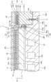
图4是第1变形例的说明图,是将基片支承体组件11的一部分放大表示的图。FIG. 4 is an explanatory view of a first modification, and is an enlarged view showing a part of the
如图4所示,在第1变形例的结构中,基片支承体101具有从上方起依次配置有静电卡盘130、电极板131和温度调节部132的结构。温度调节部132与静电卡盘130同样地通过使用设置在温度调节部132与基座131之间的金属形成的金属接合,与电极板131(下表面131d)耦合。温度调节部132与静电卡盘130同样地具有大致圆盘形状,由陶瓷形成。As shown in FIG. 4 , in the structure of the first modified example, the
在本变形例中,在静电卡盘130中内置有吸附用电极140,在温度调节部132中内置有加热器142。即,在基片支承体101中,吸附用电极140和加热器142以隔着电极板131在上下隔开间隔的方式设置。在温度调节部132的周向外侧设置有隔热部220。In this modified example, an
采用本变形例的结构,除了在上述实施方式中说明的作用效果以外,还具有如下的优点。即,基片支承体101具有将包括吸附用电极140的静电卡盘130和包括加热器142的温度调节部132在上下分离,并在静电卡盘130与温度调节部132之间夹着电极板131的构造。通过这样将吸附用电极140和加热器142分离,能够使静电卡盘130的厚度减小,其结果是,能够抑制例如400kHz等的低频侧的RF电功率的损失。另外,能够使基片W与电极板131之间的电位差减小,能够抑制基片W的背面的异常放电。According to the configuration of this modified example, in addition to the operational effects described in the above-mentioned embodiment, there are also the following advantages. That is, the
(第2变形例)(Second modified example)
图5是第2变形例的说明图,是将基片支承体组件11的一部分放大表示的图。FIG. 5 is an explanatory view of a second modification, and is an enlarged view showing a part of the
如图5所示,在第2变形例的结构中,在弹性部件160的下部设置有隔热部220。As shown in FIG. 5 , in the structure of the second modified example, a
在本变形例的结构中,电极板131与弹性部件160接触,因此,就弹性部件160而言,与弹性体制相比更优选金属制。采用本变形例,在基座100与弹性部件160之间能够得到由隔热部220产生的隔热效果,因此,与上述实施方式同样地,能够使经由弹性部件160的热传递量减少,能够高效率地使基片支承体组件11的表面温度上升。即,用于使基片W升温或保温所需要的加热器142的输出变小,因此,能够实现能量效率的提高和节能。In the structure of this modified example, since the
(第3变形例)(3rd modified example)
图6是第3变形例的说明图,是将基片支承体组件11的一部分放大表示的图。FIG. 6 is an explanatory view of a third modification, and is an enlarged view showing a part of the
如图6所示,在第3变形例的结构中,在弹性部件160的上部和下部两者设置有隔热部220(在此为第一隔热部220a和第二隔热部220b)。采用本变形例的结构,能够实现弹性部件160的周边的隔热性能的进一步提高。即,在要求使静电卡盘130成为高温的情况下,能够高效率地使静电卡盘130上升到弹性部件160的耐热温度以上的温度。As shown in FIG. 6 , in the structure of the third modified example, heat insulating parts 220 (here, first
(第4变形例)(4th modified example)
图7、图8是第4变形例的说明图,是将基片支承体组件11的一部分放大表示的图。7 and 8 are explanatory diagrams of a fourth modification, and are diagrams showing enlarged parts of the
如图7、图8所示,在第4变形例的结构中,在基座100与电极板131之间,以在隔热部220的上下夹着该隔热部220的方式配置第一弹性部件160a和第二弹性部件160b。作为具体的结构,可以是如图7所示的那样,第一弹性部件160a、第二弹性部件160b和隔热部220构成为一体的部件。或者,也可以是如图8所示的那样,第一弹性部件160a、隔热部220、第二弹性部件160b作为不同部件依次从上方起层叠配置的结构。As shown in FIGS. 7 and 8 , in the structure of the fourth modified example, between the base 100 and the
在本变形例的结构中,第一弹性部件160a的材料和第二弹性部件160b的材料可以相同,或者也可以不同。例如,一般而言,电极板131的温度比基座100的温度高,因此,可以使与电极板131接触的第一弹性部件160a为金属制,使与基座100接触的第二弹性部件160b为弹性体制。In the structure of this modified example, the material of the first
采用本变形例的结构,不需要将隔热部220与基座100和电极板131接合等。因此,除了在上述实施方式中说明的作用效果以外,还具有装置的制造变得容易的优点。According to the structure of this modification, it is not necessary to join the
此外,在上面的实施方式和变形例中,边缘环180被边缘环用静电卡盘181吸附保持,但是边缘环180的保持方法并不限于此。例如,也可以是使用吸附片来吸附保持边缘环180,还可以是通过夹持边缘环180来保持边缘环180。或者,也可以是利用边缘环180的自重来保持边缘环180。在上述情况下,边缘环用静电卡盘181可以省略。In addition, in the above embodiments and modified examples, the
Claims (17)
Applications Claiming Priority (2)
| Application Number | Priority Date | Filing Date | Title |
|---|---|---|---|
| JP2021-146247 | 2021-09-08 | ||
| JP2021146247AJP7621226B2 (en) | 2021-09-08 | 2021-09-08 | Substrate support assembly and plasma processing apparatus - Patents.com |
Publications (1)
| Publication Number | Publication Date |
|---|---|
| CN115775716Atrue CN115775716A (en) | 2023-03-10 |
Family
ID=85385746
Family Applications (1)
| Application Number | Title | Priority Date | Filing Date |
|---|---|---|---|
| CN202211052630.4APendingCN115775716A (en) | 2021-09-08 | 2022-08-31 | Substrate support assembly and plasma processing apparatus |
Country Status (5)
| Country | Link |
|---|---|
| US (1) | US20230073711A1 (en) |
| JP (1) | JP7621226B2 (en) |
| KR (1) | KR20230036975A (en) |
| CN (1) | CN115775716A (en) |
| TW (1) | TW202314853A (en) |
Families Citing this family (1)
| Publication number | Priority date | Publication date | Assignee | Title |
|---|---|---|---|---|
| WO2025046720A1 (en)* | 2023-08-29 | 2025-03-06 | 日本碍子株式会社 | Member for semiconductor manufacturing device |
Family Cites Families (15)
| Publication number | Priority date | Publication date | Assignee | Title |
|---|---|---|---|---|
| JP3347742B2 (en)* | 1997-01-02 | 2002-11-20 | シーヴイシー・プロダクツ・インコーポレーテッド | Heat conductive chuck for vacuum processing device, heat transfer device, and method for transferring heat between chuck body and substrate |
| JP2001068538A (en)* | 1999-06-21 | 2001-03-16 | Tokyo Electron Ltd | Electrode structure, mounting base structure, plasma treatment system, and processing unit |
| JP4518370B2 (en)* | 2003-07-10 | 2010-08-04 | 日本碍子株式会社 | Ceramic susceptor support structure |
| JP5482282B2 (en) | 2009-03-03 | 2014-05-07 | 東京エレクトロン株式会社 | Mounting table structure and film forming apparatus |
| JP2012028428A (en)* | 2010-07-21 | 2012-02-09 | Tokyo Electron Ltd | Mounting table structure and processing apparatus |
| US9948214B2 (en)* | 2012-04-26 | 2018-04-17 | Applied Materials, Inc. | High temperature electrostatic chuck with real-time heat zone regulating capability |
| JP6685549B2 (en)* | 2015-06-11 | 2020-04-22 | 国立研究開発法人産業技術総合研究所 | Porous body and method for producing the same |
| US20180237906A1 (en)* | 2015-08-22 | 2018-08-23 | Novena Tec Inc. | Process chamber shielding system and method |
| JP2018046185A (en)* | 2016-09-15 | 2018-03-22 | 東京エレクトロン株式会社 | Method for etching silicon oxide and silicon nitride mutually and selectively |
| JP6814337B2 (en)* | 2016-10-07 | 2021-01-20 | 日産自動車株式会社 | A member for an internal combustion engine having a heat shield film, and a method for manufacturing the member. |
| US20200035535A1 (en)* | 2018-07-27 | 2020-01-30 | Applied Materials, Inc. | Metal bonded electrostatic chuck for high power application |
| CN110911332B (en)* | 2018-09-14 | 2022-11-25 | 北京北方华创微电子装备有限公司 | Electrostatic chuck |
| JP7254542B2 (en)* | 2019-02-01 | 2023-04-10 | 東京エレクトロン株式会社 | Mounting table and substrate processing device |
| JP7340938B2 (en)* | 2019-02-25 | 2023-09-08 | 東京エレクトロン株式会社 | Mounting table and substrate processing equipment |
| JP7579758B2 (en)* | 2021-06-28 | 2024-11-08 | 東京エレクトロン株式会社 | SUBSTRATE SUPPORT, SUBSTRATE SUPPORT ASSEMBLY AND PLASMA PROCESSING APPARATUS - Patent application |
- 2021
- 2021-09-08JPJP2021146247Apatent/JP7621226B2/enactiveActive
- 2022
- 2022-08-25TWTW111132018Apatent/TW202314853A/enunknown
- 2022-08-31CNCN202211052630.4Apatent/CN115775716A/enactivePending
- 2022-09-01KRKR1020220110523Apatent/KR20230036975A/enactivePending
- 2022-09-06USUS17/903,431patent/US20230073711A1/enactivePending
Also Published As
| Publication number | Publication date |
|---|---|
| TW202314853A (en) | 2023-04-01 |
| JP2023039202A (en) | 2023-03-20 |
| US20230073711A1 (en) | 2023-03-09 |
| KR20230036975A (en) | 2023-03-15 |
| JP7621226B2 (en) | 2025-01-24 |
Similar Documents
| Publication | Publication Date | Title |
|---|---|---|
| US10304691B2 (en) | Method of etching silicon oxide and silicon nitride selectively against each other | |
| TWI887081B (en) | Plasma processing apparatus | |
| TWI449102B (en) | Plasma processing device | |
| CN108281342B (en) | Plasma processing apparatus | |
| JP7579758B2 (en) | SUBSTRATE SUPPORT, SUBSTRATE SUPPORT ASSEMBLY AND PLASMA PROCESSING APPARATUS - Patent application | |
| JP6345030B2 (en) | Plasma processing apparatus and focus ring | |
| JP2018117024A (en) | Plasma processing equipment | |
| JP2018110216A (en) | Plasma processing apparatus | |
| CN115775716A (en) | Substrate support assembly and plasma processing apparatus | |
| TW202107950A (en) | Plasma processing method and plasma processing apparatus | |
| CN117321740A (en) | Maintenance method of substrate processing device and substrate processing device | |
| JP2021141277A (en) | Mounting table and plasma processing device | |
| US12387907B2 (en) | Plasma processing apparatus and substrate processing method | |
| JP2023067767A (en) | SUBSTRATE SUPPORTER, PLASMA PROCESSING APPARATUS AND PLASMA PROCESSING METHOD | |
| CN118431142A (en) | Plasma processing apparatus, electrostatic chuck, and plasma processing method | |
| KR20240155342A (en) | Plasma treatment device and plasma treatment method | |
| US20230136720A1 (en) | Substrate support, plasma processing apparatus, and plasma processing method | |
| JP2014075281A (en) | Plasma processing apparatus and temperature control method | |
| JP2008147420A (en) | Substrate processing equipment | |
| JP2023048449A (en) | Substrate support, substrate processing apparatus and electrostatic attraction method | |
| JP2024040055A (en) | Substrate processing method and substrate processing apparatus | |
| WO2025216071A1 (en) | Substrate treatment device, substrate support, and temperature adjustment method | |
| JP2023053918A (en) | Upper electrode assembly and plasma processing apparatus | |
| JP2024027431A (en) | Plasma processing equipment and substrate support part | |
| TW202509994A (en) | Substrate support assembly and plasma processing device |
Legal Events
| Date | Code | Title | Description |
|---|---|---|---|
| PB01 | Publication | ||
| PB01 | Publication | ||
| SE01 | Entry into force of request for substantive examination | ||
| SE01 | Entry into force of request for substantive examination |