CN115731998A - Overwriting at a memory system - Google Patents
Overwriting at a memory systemDownload PDFInfo
- Publication number
- CN115731998A CN115731998ACN202211053288.XACN202211053288ACN115731998ACN 115731998 ACN115731998 ACN 115731998ACN 202211053288 ACN202211053288 ACN 202211053288ACN 115731998 ACN115731998 ACN 115731998A
- Authority
- CN
- China
- Prior art keywords
- memory
- demarcation
- voltage
- memory array
- logic states
- Prior art date
- Legal status (The legal status is an assumption and is not a legal conclusion. Google has not performed a legal analysis and makes no representation as to the accuracy of the status listed.)
- Pending
Links
Images


Classifications
- G—PHYSICS
- G06—COMPUTING OR CALCULATING; COUNTING
- G06F—ELECTRIC DIGITAL DATA PROCESSING
- G06F3/00—Input arrangements for transferring data to be processed into a form capable of being handled by the computer; Output arrangements for transferring data from processing unit to output unit, e.g. interface arrangements
- G06F3/06—Digital input from, or digital output to, record carriers, e.g. RAID, emulated record carriers or networked record carriers
- G06F3/0601—Interfaces specially adapted for storage systems
- G06F3/0628—Interfaces specially adapted for storage systems making use of a particular technique
- G06F3/0655—Vertical data movement, i.e. input-output transfer; data movement between one or more hosts and one or more storage devices
- G—PHYSICS
- G11—INFORMATION STORAGE
- G11C—STATIC STORES
- G11C16/00—Erasable programmable read-only memories
- G11C16/02—Erasable programmable read-only memories electrically programmable
- G11C16/06—Auxiliary circuits, e.g. for writing into memory
- G11C16/10—Programming or data input circuits
- G—PHYSICS
- G06—COMPUTING OR CALCULATING; COUNTING
- G06F—ELECTRIC DIGITAL DATA PROCESSING
- G06F3/00—Input arrangements for transferring data to be processed into a form capable of being handled by the computer; Output arrangements for transferring data from processing unit to output unit, e.g. interface arrangements
- G06F3/06—Digital input from, or digital output to, record carriers, e.g. RAID, emulated record carriers or networked record carriers
- G06F3/0601—Interfaces specially adapted for storage systems
- G06F3/0602—Interfaces specially adapted for storage systems specifically adapted to achieve a particular effect
- G06F3/0604—Improving or facilitating administration, e.g. storage management
- G—PHYSICS
- G06—COMPUTING OR CALCULATING; COUNTING
- G06F—ELECTRIC DIGITAL DATA PROCESSING
- G06F3/00—Input arrangements for transferring data to be processed into a form capable of being handled by the computer; Output arrangements for transferring data from processing unit to output unit, e.g. interface arrangements
- G06F3/06—Digital input from, or digital output to, record carriers, e.g. RAID, emulated record carriers or networked record carriers
- G06F3/0601—Interfaces specially adapted for storage systems
- G06F3/0668—Interfaces specially adapted for storage systems adopting a particular infrastructure
- G06F3/0671—In-line storage system
- G06F3/0673—Single storage device
- G06F3/0679—Non-volatile semiconductor memory device, e.g. flash memory, one time programmable memory [OTP]
- G—PHYSICS
- G11—INFORMATION STORAGE
- G11C—STATIC STORES
- G11C11/00—Digital stores characterised by the use of particular electric or magnetic storage elements; Storage elements therefor
- G11C11/56—Digital stores characterised by the use of particular electric or magnetic storage elements; Storage elements therefor using storage elements with more than two stable states represented by steps, e.g. of voltage, current, phase, frequency
- G11C11/5621—Digital stores characterised by the use of particular electric or magnetic storage elements; Storage elements therefor using storage elements with more than two stable states represented by steps, e.g. of voltage, current, phase, frequency using charge storage in a floating gate
- G11C11/5628—Programming or writing circuits; Data input circuits
- G11C11/5635—Erasing circuits
- G—PHYSICS
- G11—INFORMATION STORAGE
- G11C—STATIC STORES
- G11C11/00—Digital stores characterised by the use of particular electric or magnetic storage elements; Storage elements therefor
- G11C11/56—Digital stores characterised by the use of particular electric or magnetic storage elements; Storage elements therefor using storage elements with more than two stable states represented by steps, e.g. of voltage, current, phase, frequency
- G11C11/5621—Digital stores characterised by the use of particular electric or magnetic storage elements; Storage elements therefor using storage elements with more than two stable states represented by steps, e.g. of voltage, current, phase, frequency using charge storage in a floating gate
- G11C11/5642—Sensing or reading circuits; Data output circuits
- G—PHYSICS
- G11—INFORMATION STORAGE
- G11C—STATIC STORES
- G11C16/00—Erasable programmable read-only memories
- G11C16/02—Erasable programmable read-only memories electrically programmable
- G11C16/04—Erasable programmable read-only memories electrically programmable using variable threshold transistors, e.g. FAMOS
- G11C16/0483—Erasable programmable read-only memories electrically programmable using variable threshold transistors, e.g. FAMOS comprising cells having several storage transistors connected in series
- G—PHYSICS
- G11—INFORMATION STORAGE
- G11C—STATIC STORES
- G11C16/00—Erasable programmable read-only memories
- G11C16/02—Erasable programmable read-only memories electrically programmable
- G11C16/06—Auxiliary circuits, e.g. for writing into memory
- G11C16/08—Address circuits; Decoders; Word-line control circuits
- G—PHYSICS
- G11—INFORMATION STORAGE
- G11C—STATIC STORES
- G11C16/00—Erasable programmable read-only memories
- G11C16/02—Erasable programmable read-only memories electrically programmable
- G11C16/06—Auxiliary circuits, e.g. for writing into memory
- G11C16/10—Programming or data input circuits
- G11C16/14—Circuits for erasing electrically, e.g. erase voltage switching circuits
- G11C16/16—Circuits for erasing electrically, e.g. erase voltage switching circuits for erasing blocks, e.g. arrays, words, groups
- G—PHYSICS
- G11—INFORMATION STORAGE
- G11C—STATIC STORES
- G11C16/00—Erasable programmable read-only memories
- G11C16/02—Erasable programmable read-only memories electrically programmable
- G11C16/06—Auxiliary circuits, e.g. for writing into memory
- G11C16/26—Sensing or reading circuits; Data output circuits
- G—PHYSICS
- G11—INFORMATION STORAGE
- G11C—STATIC STORES
- G11C2211/00—Indexing scheme relating to digital stores characterized by the use of particular electric or magnetic storage elements; Storage elements therefor
- G11C2211/56—Indexing scheme relating to G11C11/56 and sub-groups for features not covered by these groups
- G11C2211/564—Miscellaneous aspects
- G11C2211/5641—Multilevel memory having cells with different number of storage levels
Landscapes
- Engineering & Computer Science (AREA)
- Theoretical Computer Science (AREA)
- Human Computer Interaction (AREA)
- Physics & Mathematics (AREA)
- General Engineering & Computer Science (AREA)
- General Physics & Mathematics (AREA)
- Computer Hardware Design (AREA)
- Microelectronics & Electronic Packaging (AREA)
- Techniques For Improving Reliability Of Storages (AREA)
Abstract
Translated fromChinese
Description
Translated fromChinese交叉引用cross reference
本专利申请案主张帕里(PARRY)等人2021年8月31日申请的标题为“存储器系统处的覆写(OVERWRITING AT A MEMORY SYSTEM)”的第17/462,228号美国专利申请案的优先权,所述美国专利申请案转让给本受让人并且明确地以全文引用的方式并入本文中。This patent application claims priority to U.S. Patent Application No. 17/462,228, filed August 31, 2021, by PARRY et al., entitled "OVERWRITING AT A MEMORY SYSTEM" , said US patent application is assigned to the present assignee and is expressly incorporated herein by reference in its entirety.
技术领域technical field
技术领域涉及存储器系统处的覆写。The technical field relates to overwriting at a memory system.
背景技术Background technique
存储器装置广泛用于将信息存储在例如计算机、用户装置、无线通信装置、相机、数字显示器等各种电子装置中。通过将存储器装置内的存储器单元编程为各种状态来存储信息。举例来说,二进制存储器单元可被编程为通常对应于逻辑1或逻辑0的两个支持状态中的一个。在一些实例中,单个存储器单元可支持多于两个可能的状态,所述状态中的任一者可由存储器单元存储。为了存取由存储器装置存储的信息,组件可读取或感测存储器装置内的一或多个存储器单元的状态。为了存储信息,组件可以将存储器装置内的一或多个存储器单元写入或编程到对应状态。Memory devices are widely used to store information in various electronic devices such as computers, user devices, wireless communication devices, cameras, digital displays, and the like. Information is stored by programming memory cells within a memory device into various states. For example, a binary memory cell can be programmed to one of two supported states, typically corresponding to a logical one or a logical zero. In some examples, a single memory cell can support more than two possible states, any of which can be stored by the memory cell. To access information stored by a memory device, a component may read or sense the state of one or more memory cells within the memory device. To store information, a component may write or program one or more memory cells within a memory device to a corresponding state.
存在各种类型的存储器装置,包含磁性硬盘、随机存取存储器(RAM)、只读存储器(ROM)、动态RAM(DRAM)、同步动态RAM(SDRAM)、静态RAM(SRAM)、铁电RAM(FeRAM)、磁性RAM(MRAM)、电阻式RAM(RRAM)、快闪存储器、相变存储器(PCM)、3维交叉点存储器(3D交叉点)、“或非”(NOR)和“与非”(NAND)存储器装置等。存储器装置可以是易失性或非易失性的。除非由外部电源周期性更新,否则易失性存储器单元(例如,DRAM单元)可随时间推移而丢失其编程状态。非易失性存储器单元(例如,NAND存储器单元)即使在不存在外部电源的情况下仍可在很长一段时间内维持其编程状态。Various types of memory devices exist, including magnetic hard disks, random access memory (RAM), read only memory (ROM), dynamic RAM (DRAM), synchronous dynamic RAM (SDRAM), static RAM (SRAM), ferroelectric RAM ( FeRAM), magnetic RAM (MRAM), resistive RAM (RRAM), flash memory, phase change memory (PCM), 3-dimensional cross-point memory (3D cross-point), "NOR" (NOR) and "NOR" (NAND) memory devices, etc. Memory devices can be volatile or non-volatile. Volatile memory cells (eg, DRAM cells) can lose their programmed state over time unless periodically refreshed by an external power source. Nonvolatile memory cells (eg, NAND memory cells) can maintain their programmed state for extended periods of time even in the absence of an external power source.
发明内容Contents of the invention
描述一种设备。所述设备可包含具有存储器阵列的存储器装置和与所述存储器装置耦合的控制器。所述控制器可被配置成致使所述设备:根据逻辑状态之间的第一电压分界执行写入操作以将第一信息存储于所述存储器阵列的一部分处;确定用第二信息覆写所述存储器阵列的所述部分;和基于确定覆写所述存储器阵列的所述部分,根据所述逻辑状态之间的第二电压分界执行写入操作,以将所述第二信息存储于所述存储器阵列的所述部分处。Describe a device. The apparatus can include a memory device having a memory array and a controller coupled with the memory device. The controller may be configured to cause the device to: perform a write operation to store first information at a portion of the memory array based on a first voltage demarcation between logic states; the portion of the memory array; and based on determining to overwrite the portion of the memory array, performing a write operation based on a second voltage demarcation between the logic states to store the second information in the at that portion of the memory array.
描述一种设备。所述设备可包含存储器阵列和与所述存储器阵列耦合的控制器。所述控制器可被配置成致使所述设备:接收将第一信息写入到所述存储器阵列的一部分的信令;基于所述存储器阵列的所述部分根据用于写入一数量的逻辑状态的第二电压分界被写入有第二信息,确定用于将所述数量的逻辑状态写入到所述存储器阵列的所述部分的第一电压分界;和根据用于写入所述数量的逻辑状态的所述确定的第一电压分界,将所述第一信息写入到所述存储器阵列的所述部分。Describe a device. The apparatus can include a memory array and a controller coupled with the memory array. The controller may be configured to cause the device to: receive signaling to write first information to a portion of the memory array; A second voltage demarcation of a second voltage demarcation is written with second information, determining a first voltage demarcation for writing the number of logic states to the portion of the memory array; and The determined first voltage demarcation of logic states writes the first information to the portion of the memory array.
描述一种设备。所述设备可包含包括存储器阵列的存储器装置和与所述存储器装置耦合的控制器。所述控制器可被配置成致使所述设备:从主机装置接收读取所述存储器阵列的被写入有一数量的逻辑状态的部分的读取命令;确定所述存储器阵列的所述部分是根据逻辑状态之间的第一电压分界还是根据所述逻辑状态之间的第二电压分界被写入有所述数量的逻辑状态;和将读取所述存储器阵列的所述部分的信令发射到所述存储器装置,其中所述信令包括所述存储器阵列的所述部分的指示以及所述存储器阵列的所述部分是根据所述逻辑状态之间的所述第一电压分界还是根据所述逻辑状态之间的所述第二电压分界被写入有所述数量的逻辑状态的指示。Describe a device. The apparatus can include a memory device including a memory array and a controller coupled with the memory device. The controller may be configured to cause the apparatus to: receive a read command from a host device to read a portion of the memory array written with a number of logic states; determine that the portion of the memory array is based on whether the first voltage demarcation between logic states is written with the number of logic states according to the second voltage demarcation between the logic states; and transmitting signaling to read the portion of the memory array to The memory device, wherein the signaling includes an indication of the portion of the memory array and whether the portion of the memory array is according to the first voltage demarcation between the logic states or according to the logic state The second voltage demarcation between states is written with an indication of the number of logic states.
描述一种设备。所述设备可包含存储器阵列和与所述存储器阵列耦合的控制器。所述控制器可被配置成致使所述设备:从存储器系统的控制器接收从所述存储器阵列的被写入有一数量的逻辑状态的部分读取信息的信令;基于所述存储器阵列的所述部分是根据逻辑状态之间的第一电压分界还是根据所述逻辑状态之间的第二电压分界被写入有所述数量的逻辑状态,在第一读取电压分界和第二读取电压分界之间进行选择;和至少部分地基于所述选择的第一读取电压分界或所述选择的第二读取电压分界,对所述存储器阵列的所述部分执行读取操作。Describe a device. The apparatus can include a memory array and a controller coupled with the memory array. The controller may be configured to cause the device to: receive signaling from a controller of a memory system to read information from a portion of the memory array written with a number of logic states; Whether said portion is written with said number of logic states according to a first voltage demarcation between logic states or according to a second voltage demarcation between said logic states, between the first read voltage demarcation and the second read voltage demarcation selecting between demarcations; and performing a read operation on the portion of the memory array based at least in part on the selected first read voltage demarcation or the selected second read voltage demarcation.
附图说明Description of drawings
图1说明根据本文所公开的实例的支持存储器系统处的覆写的系统的实例。1 illustrates an example of a system that supports overwriting at a memory system according to examples disclosed herein.
图2说明根据本文所公开的实例的支持存储器系统处的覆写的存储器装置的实例。2 illustrates an example of a memory device that supports overwriting at a memory system according to examples disclosed herein.
图3说明根据本文所公开的实例的支持存储器系统处的覆写的存储器电路的实例。3 illustrates an example of a memory circuit that supports overwriting at a memory system according to examples disclosed herein.
图4和5说明根据本文所公开的实例的支持存储器系统处的覆写的覆写方案的实例。4 and 5 illustrate examples of overwrite schemes that support overwrite at a memory system according to examples disclosed herein.
图6A和6B说明根据本文所公开的实例的支持存储器系统处的覆写的过程流的实例。6A and 6B illustrate an example of a process flow to support overwriting at a memory system according to examples disclosed herein.
图7说明根据本文所公开的实例的支持存储器系统处的覆写的覆写映射的实例。7 illustrates an example of an overwrite map that supports overwriting at a memory system according to examples disclosed herein.
图8说明根据本文所公开的实例的支持存储器系统处的覆写的存储器系统的框图。8 illustrates a block diagram of a memory system that supports overwriting at a memory system according to examples disclosed herein.
图9示出根据本文所公开的实例的支持存储器系统处的覆写的存储器装置的框图。9 shows a block diagram of a memory device supporting overwriting at a memory system according to examples disclosed herein.
图10到13示出说明根据本文所公开的实例的支持存储器系统处的覆写的一或多种方法的流程图。10-13 show flowcharts illustrating one or more methods of supporting overwriting at a memory system according to examples disclosed herein.
具体实施方式Detailed ways
存储器系统可包含根据各种存储架构操作的一或多个存储器装置。存储器装置可包含存储器单元阵列和可操作以对存储器单元执行存取操作的电路系统。在一些存储架构中,存储器装置的存储器单元可被写入以存储特定逻辑状态,并且可在被写入以存储不同逻辑状态或以其它方式存储不同信息之前经擦除。举例来说,在NAND存储器架构中,可通过将电荷存储于晶体管的浮动栅极上来写入NAND存储器单元,这可影响用于激活存储器单元的阈值电压,或可影响当晶体管激活时流过晶体管的电流的量,可感测所述电流量以用于检测存储器单元所存储的逻辑状态。在一些情况下,写入到存储器阵列中的一些数据部分可为暂时的(例如,可在一定时间之后变得无效)。在一些实例中,为了用不同信息写入NAND存储器阵列的一部分,可首先通过移除或以其它方式改变存储于NAND存储器阵列的所述部分的晶体管的浮动栅极上的电荷的量来擦除NAND存储器阵列的所述部分。然而,在这些和其它实例中,擦除存储器单元或以其它方式改变存储器单元的状态(例如,翻转以其它方式改变的逻辑状态的位)可与功率消耗、时延或存储器单元降级或耗损以及其它缺陷相关联。A memory system may include one or more memory devices operating according to various memory architectures. A memory device may include an array of memory cells and circuitry operable to perform access operations on the memory cells. In some memory architectures, memory cells of a memory device can be written to store a particular logic state, and can be erased before being written to store a different logic state or otherwise store different information. For example, in a NAND memory architecture, a NAND memory cell can be written by storing charge on the transistor's floating gate, which can affect the threshold voltage used to activate the memory cell, or can affect the charge that flows through the transistor when it is activated. The amount of current that can be sensed for detecting the logic state stored by the memory cell. In some cases, some portions of data written into the memory array may be temporary (eg, may become invalid after a certain time). In some examples, to write a portion of a NAND memory array with different information, it may first be erased by removing or otherwise changing the amount of charge stored on the floating gates of the transistors of that portion of the NAND memory array. the portion of the NAND memory array. However, in these and other examples, erasing a memory cell or otherwise changing the state of a memory cell (e.g., flipping a bit of an otherwise changed logic state) can be correlated with power consumption, latency, or memory cell degradation or wear and Associated with other defects.
根据本文所公开的实例,存储器系统的一或多个组件可被配置成用新数据覆写存储器阵列的部分,这可与省略擦除操作(例如,根据“无擦除的重复使用”配置)相关联。举例来说,存储器系统的组件可根据第一分界(例如,第一分界配置、与相应逻辑状态相关联的第一写入信号集、用于区分写入的逻辑状态的一或多个参考信号的第一集)执行写入操作以将信息存储于存储器阵列的一部分处。在这类写入操作之后,存储器系统的组件可确定用不同的或经更新的信息覆写存储器阵列的所述部分,这可包含根据第二分界(例如,第二分界配置、与相应逻辑状态相关联的第二写入信号集、用于区分写入的逻辑状态的一或多个参考信号的第二集)执行写入操作。在一些实例中,第二分界可与针对给定逻辑状态的不同单元特性相关联,所述不同单元特性例如存储的电荷或其它单元性质的不同分布、不同分界特性(例如,不同参考电压)、不同写入操作(例如,不同写入电压、不同写入电流),以及其它差异。According to examples disclosed herein, one or more components of a memory system may be configured to overwrite portions of a memory array with new data, which may be the same as omitting an erase operation (e.g., according to a "reuse without erase" configuration) Associated. For example, components of a memory system may be configured according to a first demarcation (e.g., a first demarcation, a first set of write signals associated with corresponding logic states, one or more reference signals used to distinguish written logic states A first set of ) performs a write operation to store information at a portion of the memory array. After such a write operation, components of the memory system may determine to overwrite the portion of the memory array with different or updated information, which may include An associated second set of write signals, a second set of one or more reference signals for distinguishing the logic state of the write) performs the write operation. In some examples, the second demarcation may be associated with different cell characteristics for a given logic state, such as a different distribution of stored charge or other cell properties, different demarcation characteristics (e.g., different reference voltages), Different write operations (eg, different write voltages, different write currents), and other differences.
在一些实施方案中,存储器系统的组件可将待存储于存储器单元处的新状态(例如,在覆写之后的所要逻辑状态)与待写入目标存储器单元的当前状态(例如,与先前写入的信息相关联的逻辑状态)进行比较。如果目标存储器单元的状态不对应于新逻辑状态,那么存储器系统的组件可确定根据覆写分界配置用新状态覆写目标存储器单元。如果目标存储器单元的状态确实对应于新逻辑状态,那么存储器系统的组件可确定制止执行覆写操作,这相较于其中执行覆写操作的情形可另外减小功率消耗或降低存储器单元疲乏。在一些实例中,用于与分界的数量增加(例如,参考电压的数量增加),或针对相应数量的逻辑状态的单元特性分布的数量增加相关联的覆写的分界配置可支持此类技术。In some implementations, components of the memory system may compare the new state to be stored at the memory cell (e.g., the desired logical state after overwriting) with the current state to be written to the target memory cell (e.g., the same as the previously written The logical state associated with the information) is compared. If the state of the target memory cell does not correspond to the new logical state, components of the memory system may determine to overwrite the target memory cell with the new state according to the overwrite demarcation configuration. If the state of the target memory cell does correspond to the new logic state, components of the memory system may determine to refrain from performing the overwrite operation, which may additionally reduce power consumption or reduce memory cell fatigue compared to situations in which the overwrite operation is performed. In some examples, demarcation configurations for overrides associated with an increased number of demarcations (eg, an increased number of reference voltages), or an increased number of cell characteristic distributions for a corresponding number of logic states may support such techniques.
在一些实施方案中,存储器系统可多次覆写存储器阵列的同一部分。在每一覆写遍次处,取决于正在写入的新信息,可覆写或保留有效和无效数据的不同部分。存储器系统的组件可存储与存储器阵列的一或多个部分的覆写条件相关的信息,所述信息可用于识别针对存储器阵列的相应部分的恰当读取分界,或评估存储器阵列的相应部分是否可用于后续覆写(例如,被配置成支持覆写,处于支持另一覆写操作的条件中),以及其它目的。可在垃圾收集操作期间实施如本文中所公开的覆写方案,以用于更新系统表(例如,逻辑到物理(L2P)表),用于重复使用写入助推器存储器块,或用于数个其它应用程序,包含其中信息存储是相对瞬态的那些应用程序,或用于存储器阵列(例如,子阵列、平面、块)的被配置成用于存储或分配给存储相对瞬态信息(例如,相对有可能改变的信息)的部分。根据这些和其它实例,通过用选择性地省略擦除相关联存储器单元的一或多个方面的写入操作来覆写存储器单元,存储器系统可在存储器降级减小、功率消耗减小或阵列可用性提高(可支持较长操作寿命(例如,更大数量的总写入字节(TBW)、更大编程/擦除耐久性额定值或其它使用寿命度量)、或超量配给的程度减小(例如,可分配用于例如垃圾收集的存储器管理或用于存储器单元引退的备用存储器单元的数量减小)以及其它益处下操作。In some implementations, the memory system can overwrite the same portion of the memory array multiple times. At each overwrite pass, depending on the new information being written, different portions of valid and invalid data may be overwritten or preserved. Components of a memory system may store information related to an overwrite condition of one or more portions of a memory array that may be used to identify an appropriate read demarcation for the corresponding portion of the memory array, or to assess whether the corresponding portion of the memory array is usable For subsequent overwrites (eg, configured to support an overwrite, in a condition to support another overwrite operation), and for other purposes. Overwrite schemes as disclosed herein may be implemented during garbage collection operations for updating system tables (e.g., logical-to-physical (L2P) tables), for reusing write booster memory blocks, or for Several other applications, including those in which information storage is relatively transient, or for memory arrays (e.g., subarrays, planes, blocks) that are configured to store or allocated to store relatively transient information ( For example, relative information that is likely to change) section. According to these and other examples, by overwriting a memory cell with a write operation that selectively omits one or more aspects of erasing the associated memory cell, a memory system may experience reduced memory degradation, reduced power consumption, or array availability. Increased (may support longer operating life (e.g., greater number of Total Bytes Written (TBW), greater program/erase endurance ratings, or other measure of useful life), or reduced degree of over-provisioning ( For example, memory management, such as garbage collection, or a reduced number of spare memory cells for memory cell retirement may be allocated to operate under, among other benefits.
在如参考图1到3所描述的系统、装置和电路的上下文中描述本公开的特征。在参考图4-7的覆写方案、过程流和覆写映射的上下文中描述本公开的特征。在参考8-13的涉及存储器系统处的覆写的设备图和流程图的上下文中进一步说明和描述本公开的这些和其它特征。The features of the present disclosure are described in the context of the systems, devices and circuits as described with reference to FIGS. 1-3. Features of the present disclosure are described in the context of the override schemes, process flows, and override maps with reference to Figures 4-7. These and other features of the present disclosure are further illustrated and described in the context of the apparatus diagrams and flowcharts of references 8-13 involving overwriting at a memory system.
图1说明根据本文所公开的实例的支持存储器系统处的覆写的系统100的实例。系统100包含与存储器系统110耦接的主机系统105。1 illustrates an example of a
存储器系统110可为或包含任何装置或装置的集合,其中所述装置或装置的集合包含至少一个存储器阵列。例如,存储器系统110可为或包含通用快闪存储(UFS)装置、嵌入式多媒体控制器(eMMC)装置、快闪装置、通用串行总线(USB)快闪装置、安全数字(SD)卡、固态驱动器(SSD)、硬盘驱动器(HDD)、双列直插式存储器模块(DIMM)、小型DIMM(SO-DIMM),或非易失性DIMM(NVDIMM),以及其它可能性。Memory system 110 may be or include any device or collection of devices that includes at least one memory array. For example, the memory system 110 may be or include a universal flash storage (UFS) device, an embedded multimedia controller (eMMC) device, a flash device, a universal serial bus (USB) flash device, a secure digital (SD) card, Solid State Drives (SSD), Hard Disk Drives (HDD), Dual Inline Memory Modules (DIMMs), Small Outline DIMMs (SO-DIMMs), or Non-Volatile DIMMs (NVDIMMs), among other possibilities.
系统100可包含在计算装置中,所述计算装置如台式计算机、手提式计算机、网络服务器、移动装置、交通工具(例如,飞机、无人机、火车、汽车或其它运输工具)、具物联网(IoT)功能的装置、嵌入式计算机(例如,包含在交通工具、工业设备或联网商业装置中的嵌入式计算机),或包含存储器和处理装置的任何其它计算装置。The
系统100可包含可与存储器系统110耦合的主机系统105。在一些实例中,此耦合可包含与主机系统控制器106的接口,所述主机系统控制器106可以是配置成使得主机系统105根据如本文中所描述的实例执行各种操作的控制器或控制组件的实例。主机系统105可包含一或多个装置,并且在一些情况下,可包含处理器芯片组和由处理器芯片组执行的软件堆栈。例如,主机系统105可包含被配置成用于与存储器系统110或其中的装置通信的应用程序。处理器芯片组可包含一或多个核心、一或多个高速缓存(例如,主机系统105本地的或包含在主机系统105中的存储器)、存储器控制器(例如,NVDIMM控制器),和存储协议控制器(例如,外围组件互连高速(PCIe)控制器、串行高级技术附件(SATA)控制器)。主机系统105可使用存储器系统110例如将数据写入到存储器系统110以及从存储器系统110读取数据。虽然图1中示出一个存储器系统110,但主机系统105可与任何数量的存储器系统110耦合。
主机系统105可以经由至少一个物理主机接口与存储器系统110耦合。在一些情况下,主机系统105和存储器系统110可被配置成使用相关联协议经由物理主机接口通信(例如,以在存储器系统110与主机系统105之间交换或以其它方式传达控制、地址、数据和其它信号)。物理主机接口的实例可包含但不限于SATA接口、UFS接口、eMMC接口、PCIe接口、USB接口、光纤通道接口、小型计算机系统接口(SCSI)、串行连接的SCSI(SAS)、双数据速率(DDR)接口、DIMM接口(例如,支持DDR的DIMM套接接口)、开放NAND快闪接口(ONFI),以及低功率双数据速率(LPDDR)接口。在一些实例中,一或多个此类接口可包含在主机系统105的主机系统控制器106与存储器系统110的存储器系统控制器115中或以其它方式在其间得到支持。在一些实例中,主机系统105可经由用于包含在存储器系统110中的每一存储器装置130的相应物理主机接口或经由用于包含在存储器系统110中的每一类型的存储器装置130的相应物理主机接口而与存储器系统110耦合(例如,主机系统控制器106可与存储器系统控制器115耦合)。Host system 105 may be coupled with memory system 110 via at least one physical host interface. In some cases, host system 105 and memory system 110 may be configured to communicate via a physical host interface using an associated protocol (e.g., to exchange or otherwise communicate control, addresses, data, etc. between memory system 110 and host system 105). and other signals). Examples of physical host interfaces may include, but are not limited to, SATA interfaces, UFS interfaces, eMMC interfaces, PCIe interfaces, USB interfaces, Fiber Channel interfaces, Small Computer System Interface (SCSI), Serial Attached SCSI (SAS), Double Data Rate ( DDR) interface, DIMM interface (eg, DDR-capable DIMM socket), Open NAND Flash Interface (ONFI), and Low Power Double Data Rate (LPDDR) interface. In some examples, one or more such interfaces may be included in or otherwise supported between host system controller 106 of host system 105 and memory system controller 115 of memory system 110 . In some examples, host system 105 can communicate via a corresponding physical host interface for each memory device 130 included in memory system 110 or via a corresponding physical host interface for each type of memory device 130 included in memory system 110 . A host interface is coupled to memory system 110 (eg, host system controller 106 may be coupled to memory system controller 115).
存储器系统110可包含存储器系统控制器115和一或多个存储器装置130。存储器装置130可以包含任何类型的存储器单元(例如,非易失性存储器单元、易失性存储器单元,或其任何组合)的一或多个存储器阵列。虽然图1的实例中展示两个存储器装置130-a和130-b,但存储器系统110可包含任何数量的存储器装置130。此外,如果存储器系统110包含多于一个存储器装置130,那么存储器系统110内的不同存储器装置130可包含相同或不同类型的存储器单元。Memory system 110 may include a memory system controller 115 and one or more memory devices 130 . Memory device 130 may include one or more memory arrays of any type of memory cells, such as non-volatile memory cells, volatile memory cells, or any combination thereof. Although two memory devices 130-a and 130-b are shown in the example of FIG. 1 , memory system 110 may include any number of memory devices 130 . Furthermore, if memory system 110 includes more than one memory device 130, different memory devices 130 within memory system 110 may include the same or different types of memory cells.
存储器系统控制器115可与主机系统105耦合和通信(例如,经由物理主机接口)并且可为被配置成致使存储器系统110根据如本文中所描述的实例执行各种操作的控制器、控制组件或固件的实例。存储器系统控制器115还可与存储器装置130耦合并通信以在存储器装置130处执行一般可称为存取操作的操作,例如读取数据、写入数据、擦除数据或刷新数据,以及其它此类操作。在一些情况下,存储器系统控制器115可从主机系统105接收命令且与一或多个存储器装置130通信以执行此些命令(例如,在所述一或多个存储器装置130内的存储器阵列处)。举例来说,存储器系统控制器115可从主机系统105接收命令或操作并且可将所述命令或操作转换成指令或适当命令以实现对存储器装置130的所要存取。在一些情况下,存储器系统控制器115可与主机系统105以及一或多个存储器装置130交换数据(例如,响应于或以其它方式结合来自主机系统105的命令)。例如,存储器系统控制器115可以将与存储器装置130相关联的响应(例如,数据分组或其它信号)转换成用于主机系统105的相应信号。Memory system controller 115 may be coupled to and communicate with host system 105 (e.g., via a physical host interface) and may be a controller, control component, or controller configured to cause memory system 110 to perform various operations according to examples as described herein. An instance of firmware. Memory system controller 115 may also couple and communicate with memory device 130 to perform operations at memory device 130 that may generally be referred to as access operations, such as reading data, writing data, erasing data, or refreshing data, among others. class operation. In some cases, memory system controller 115 may receive commands from host system 105 and communicate with one or more memory devices 130 to execute such commands (e.g., at a memory array within the one or more memory devices 130 ). For example, memory system controller 115 may receive commands or operations from host system 105 and may convert the commands or operations into instructions or appropriate commands to achieve the desired access to memory device 130 . In some cases, memory system controller 115 may exchange data with host system 105 and one or more memory devices 130 (eg, in response to or otherwise in conjunction with commands from host system 105 ). For example, memory system controller 115 may convert responses (eg, data packets or other signals) associated with memory device 130 into corresponding signals for host system 105 .
存储器系统控制器115可配置成用于与存储器装置130相关联的其它操作。举例来说,存储器系统控制器115可执行或管理操作,例如耗损均衡操作、垃圾收集操作、例如错误检测操作或错误校正操作的错误控制操作、引退操作、加密操作、高速缓存操作、媒体管理操作、后台刷新、健康监测,以及与来自主机系统105的命令相关联的逻辑地址(例如,逻辑块地址(LBA))和与存储器装置130内的存储器单元相关联的物理地址(例如,物理块地址)之间的地址转译。Memory system controller 115 may be configured for other operations associated with memory device 130 . For example, memory system controller 115 may perform or manage operations such as wear leveling operations, garbage collection operations, error control operations such as error detection operations or error correction operations, retirement operations, encryption operations, caching operations, media management operations , background refresh, health monitoring, and logical addresses (e.g., Logical Block Addresses (LBAs)) associated with commands from host system 105 and physical addresses (e.g., Physical Block Addresses) associated with memory cells within memory device 130 ) address translation between.
存储器系统控制器115可包含硬件,如一或多个集成电路或离散组件、缓冲存储器或其组合。硬件可包含具有专用(例如,硬译码)逻辑的电路系统以执行本文中归于存储器系统控制器115的操作。存储器系统控制器115可为或包含微控制器、专用逻辑电路系统(例如,现场可编程门阵列(FPGA)、专用集成电路(ASIC)、数字信号处理器(DSP)),或任何其它合适的处理器或处理电路。Memory system controller 115 may include hardware such as one or more integrated circuits or discrete components, cache memory, or a combination thereof. The hardware may include circuitry with dedicated (eg, hard-coded) logic to perform the operations ascribed to memory system controller 115 herein. Memory system controller 115 may be or include a microcontroller, dedicated logic circuitry (e.g., field programmable gate array (FPGA), application specific integrated circuit (ASIC), digital signal processor (DSP)), or any other suitable processor or processing circuit.
存储器系统控制器115还可包含本地存储器120。在一些情况下,本地存储器120可包含只读存储器(ROM)或其它可存储操作代码(例如,可执行指令)的存储器,所述操作代码可由存储器系统控制器115执行以执行本文中属于存储器系统控制器115的功能。在一些情况下,本地存储器120可另外或替代地包含静态随机存取存储器(SRAM)或其它可供存储器系统控制器115用于内部存储或计算的存储器,例如,与本文中属于存储器系统控制器115的功能有关的内部存储或计算。另外或替代地,本地存储器120可用作存储器系统控制器115的高速缓存。例如,如果从存储器装置130读取或向其写入,那么数据可以存储在本地存储器120中,并且数据可在本地存储器120内供主机系统105(例如,相对于存储器装置130具有减小的时延)用于后续根据高速缓存策略进行检索或操控(例如,更新)。The memory system controller 115 may also include a local memory 120 . In some cases, local memory 120 may include read-only memory (ROM) or other memory that can store operational code (eg, executable instructions) that is executable by memory system controller 115 to perform the functions described herein in terms of memory system Function of the controller 115 . In some cases, local memory 120 may additionally or alternatively comprise static random access memory (SRAM) or other memory available to memory system controller 115 for internal storage or computation, for example, as described herein with respect to memory system controller 115 functions related to internal storage or computation. Additionally or alternatively, local memory 120 may serve as a cache for memory system controller 115 . For example, if reading from or writing to memory device 130, the data can be stored in local memory 120 and the data can be made available to host system 105 within local memory 120 (e.g., with reduced time relative to memory device 130). extension) for subsequent retrieval or manipulation (eg, update) according to the cache policy.
虽然图1中的存储器系统110的实例已说明为包含存储器系统控制器115,但在某些情况下,存储器系统110可不包含存储器系统控制器115。举例来说,存储器系统110可另外或替代地依赖于外部控制器或固件(例如,由主机系统105实施)或可在存储器装置130内部的一或多个本地控制器135以分别执行本文中属于存储器系统控制器115的功能。一般来说,本文中属于存储器系统控制器115的一或多个功能可在一些情况下替代地由主机系统105、本地控制器135或其任何组合执行。在一些情况下,至少部分地由存储器系统控制器115管理的存储器装置130可称为受管理存储器装置。受管理存储器装置的实例是受管理NAND(MNAND)装置。Although the example of memory system 110 in FIG. 1 has been illustrated as including memory system controller 115 , in some cases memory system 110 may not include memory system controller 115 . For example, memory system 110 may additionally or alternatively rely on an external controller or firmware (e.g., implemented by host system 105) or one or more
存储器装置130可以包含非易失性存储器单元的一或多个阵列。举例来说,存储器装置130可包含NAND(例如,NAND快闪)存储器、ROM、相变存储器(PCM)、自选存储器、其它基于硫族化物的存储器、铁电随机存取存储器(RAM)(FeRAM)、磁性RAM(MRAM)、NOR(例如,NOR快闪)存储器、自旋转移力矩(STT)-MRAM、导电桥接RAM(CBRAM)、电阻式随机存取存储器(RRAM)、基于氧化物的RRAM(OxRAM)、电可擦除可编程ROM(EEPROM),或其任何组合。另外或替代地,存储器装置130可以包含易失性存储器单元的一或多个阵列。举例来说,存储器装置130可包含RAM存储器单元,例如动态RAM(DRAM)存储器单元和同步DRAM(SDRAM)存储器单元。Memory device 130 may include one or more arrays of non-volatile memory cells. For example, memory device 130 may include NAND (eg, NAND flash) memory, ROM, phase change memory (PCM), self-select memory, other chalcogenide-based memory, ferroelectric random access memory (RAM) (FeRAM ), Magnetic RAM (MRAM), NOR (eg, NOR flash) memory, spin transfer torque (STT)-MRAM, conductive bridge RAM (CBRAM), resistive random access memory (RRAM), oxide-based RRAM (OxRAM), Electrically Erasable Programmable ROM (EEPROM), or any combination thereof. Additionally or alternatively, memory device 130 may include one or more arrays of volatile memory cells. For example, memory device 130 may include RAM memory cells, such as dynamic RAM (DRAM) memory cells and synchronous DRAM (SDRAM) memory cells.
在一些实例中,存储器装置130可以(例如,在同一裸片上或在同一封装内)包含本地控制器135,其可以对相应存储器装置130的一或多个存储器单元执行操作。本地控制器135可结合存储器系统控制器115操作,或可执行本文中归于存储器系统控制器115的一或多个功能。举例来说,如图1所说明,存储器装置130-a可以包含本地控制器135-a,且存储器装置130-b可以包含本地控制器135-b。In some examples, memory devices 130 may include (eg, on the same die or within the same package) a
在一些情况下,存储器装置130可以是或包含NAND装置(例如,NAND快闪装置)。存储器装置130可以是或包含存储器裸片160。举例来说,在一些情况下,存储器装置130可为包含一或多个裸片160的封装。在一些实例中,裸片160可以是从晶片切割的一块电子级半导体(例如,从硅晶片切割的硅裸片)。每个裸片160可包含一或多个平面165,且每个平面165可包含相应的一组块170,其中每个块170可包含相应的一组页175,且每个页175可包含一组存储器单元。In some cases, memory device 130 may be or include a NAND device (eg, a NAND flash device). Memory device 130 may be or include memory die 160 . For example, in some cases, memory device 130 may be a package including one or
在一些情况下,NAND存储器装置130可包含被配置成各自存储一个信息位的存储器单元,其可被称为单层级单元(SLC)。另外或替代地,NAND存储器装置130可以包含被配置成各自存储多个信息位的存储器单元,如果被配置成各自存储两个信息位,则其可以被称为多层级单元(MLC),如果被配置成各自存储三个信息位,则其可以被称为三层级单元(TLC),如果被配置成各自存储四个信息位,则其可以被称为四层级单元(QLC),或更一般地被称为多层级存储器单元。多层级存储器单元可相对于SLC存储器单元提供更大的存储密度,但在一些情况下,可能涉及用于支持电路系统的更窄读取或写入容限或更大复杂度。In some cases, NAND memory device 130 may include memory cells configured to each store one bit of information, which may be referred to as single-level cells (SLCs). Additionally or alternatively, NAND memory device 130 may include memory cells configured to each store a plurality of bits of information, which may be referred to as a multi-level cell (MLC) if configured to each store two bits of information, if referred to as Configured to store three bits of information each, they may be referred to as triple-level cells (TLCs), if configured to store four bits of information each, they may be referred to as quad-level cells (QLCs), or more generally Known as a multi-level memory cell. Multi-level memory cells may provide greater storage density relative to SLC memory cells, but in some cases may involve narrower read or write margins or greater complexity for supporting circuitry.
在一些情况下,平面165可指块170的群组,并且在一些情况下,可在不同平面165内进行并发操作。例如,可对不同块170内的存储器单元进行并行操作,只要不同块170处于不同平面165中即可。在一些情况下,个别块170可被称作物理块,并且虚拟块180可指可在其内发生并行操作的块170的群组。举例来说,可对分别在平面165-a、165-b、165c和165-d内的块170-a、170-b、170-c和170-d进行并行操作,且块170-a、170-b、170-c和170-d可统称为虚拟块180。在一些情况下,虚拟块可包含来自不同存储器装置130的块170(例如,包含存储器装置130-a和存储器装置130-b的一或多个平面中的块)。在一些情况下,虚拟块内的块170可在其相应平面165内具有相同的块地址(例如,块170-a可为平面165-a的“块0”,块170-b可为平面165-b的“块0”,等等)。在一些情况下,在不同平面165中进行并行操作可受制于一或多个限制,如对不同页175内的存储器单元进行并行操作,所述存储器单元在其相应平面165内具有相同页地址(例如,与命令解码、页地址解码电路系统,或跨平面165共享的其它电路系统相关)。In some cases, a
在一些情况下,块170可包含组织成行(页175)和列(例如,串,未展示)的存储器单元。例如,同一页175中的存储器单元可共享共同字线(例如,与其耦合),并且同一串中的存储器单元可共享共同数字线(其可替代地被称为位线)(例如,与其耦合)。In some cases, block 170 may include memory cells organized into rows (page 175) and columns (eg, strings, not shown). For example, memory cells in the
对于一些NAND架构,存储器单元可在第一粒度级别(例如,在页粒度级别)读取和编程(例如,写入),但可在第二粒度级别(例如,在块粒度级别)擦除。也就是说,页175可为可独立地编程或读取(例如,作为单个编程或读取操作的一部分同时编程或读取)的存储器(例如,存储器单元的集合)的最小单元,且块170可为可独立地擦除(例如,作为单个擦除操作的一部分同时擦除)的存储器(例如,存储器单元的集合)的最小单元。此外,在一些情况下,NAND存储器单元可在其可用新数据重写之前进行擦除。因此,举例来说,在一些情况下,可直到包含页175的整个块170已被擦除才更新所使用的页175。For some NAND architectures, memory cells can be read and programmed (eg, written) at a first granularity level (eg, at a page granularity level), but erased at a second granularity level (eg, at a block granularity level). That is,
在一些情况下,为了更新块170内的一些数据同时保留块170内的其它数据,存储器装置130可以将待保留的数据复制到新块170且将更新后的数据写入到新块170的一或多个其余页。存储器装置130(例如,本地控制器135)或存储器系统控制器115可将保持在旧块170中的数据标记或以其它方式指定为无效或过时,且更新逻辑到物理(L2P)映射表以使数据的逻辑地址(例如,LBA)与新的有效块170而不是旧的无效块170相关联。在一些情况下,例如归因于时延或耗损考虑因素,可执行此类复制和重新映射而非擦除和重写整个旧块170。在一些情况下,L2P映射表的一或多个副本可存储在存储器装置130的存储器单元内(例如,或多个块170或平面165内),以供本地控制器135或存储器系统控制器115使用(例如,参考和更新)。In some cases, in order to update some data within
在一些情况下,可以维持L2P映射表且可以页级别的粒度将数据标记为有效或无效的,并且页175可以包含有效数据、无效数据或不包含数据。无效数据可以是由于数据的较新版本或更新版本存储在存储器装置130的不同页175中而过时的数据。无效数据先前可能已被编程到无效页175,但可能不再与有效逻辑地址(例如由主机系统105参考的逻辑地址)相关联。有效数据可以是存储在存储器装置130上的此类数据的最新版本。不包含数据的页175可以是从未被写入或已被擦除的页175。In some cases, an L2P mapping table may be maintained and data may be marked as valid or invalid at page level granularity, and
在一些情况下,存储器系统控制器115或本地控制器135可执行存储器装置130的操作(例如,作为一或多个媒体管理算法的部分),例如耗损均衡、后台刷新、垃圾收集、擦除、块扫描、健康监测、单元或子阵列引退(例如,块170的引退)或其它,或其任何组合。例如,在存储器装置130内,块170可以具有包含有效数据的一些页175和包含无效数据的一些页175。为了避免等待块170中的所有页175具有无效数据以便擦除和重复使用块170,可调用被称作“垃圾收集”的算法,以允许块170被擦除和释放为用于后续写入操作的空闲块。垃圾收集可指媒体管理操作集,其包含例如选择包含有效和无效数据的块170、选择块中包含有效数据的页175、将来自所选页175的有效数据复制到新位置(例如,另一块170中的空闲页175)、将先前选择的页175中的数据标记为无效,以及擦除选定块170。因此,可增加已擦除的块170的数量,使得可使用更多的块170来存储后续数据(例如,随后从主机系统105接收到的数据)。In some cases, memory system controller 115 or
系统100可包含支持存储器系统处的覆写的任何数量的非暂时性计算机可读媒体。例如,主机系统105、存储器系统控制器115或存储器装置130(例如,本地控制器135)可包含或以其它方式可存取一或多个非暂时性计算机可读媒体,所述非暂时性计算机可读媒体存储指令(例如,固件)以进行本文中归于主机系统105、存储器系统控制器115或存储器装置130的功能。举例来说,此类指令可在由主机系统105(例如,由主机系统控制器106)、由存储器系统控制器115或由存储器装置130(例如,由本地控制器135)执行的情况下,致使主机系统105、存储器系统控制器115或存储器装置130执行如本文中所描述的一或多个相关联功能。
在一些情况下,存储器系统110可利用存储器系统控制器115以提供受管理存储器系统,所述受管理存储器系统可包含例如一或多个存储器阵列和与本地(例如,裸片上或封装中)控制器(例如,本地控制器135)组合的相关电路系统。受管理存储器系统的实例为受管理NAND(MNAND)系统。In some cases, memory system 110 may utilize memory system controller 115 to provide a managed memory system that may include, for example, one or more memory arrays and local (e.g., on-die or in-package) control associated circuitry combined with a controller (eg, local controller 135). An example of a managed memory system is a managed NAND (MNAND) system.
根据本文所公开的实例,存储器系统110的一或多个组件可被配置成支持用新数据覆写(例如,存储器裸片160的)存储器阵列的部分,这可与省略擦除操作相关联。举例来说,存储器系统110的组件可根据第一分界配置执行写入操作以将信息存储于存储器阵列的一部分处。在这类写入操作之后,存储器系统110的组件可确定用不同的或经更新的信息覆写存储器阵列的所述部分,这可包含根据第二分界配置执行写入操作。在一些实例中,第二分界配置可与针对给定逻辑状态的不同单元特性相关联,所述不同单元特性例如存储的电荷或其它单元性质的不同分布、不同分界特性、或不同写入操作配置,以及其它差异。通过用选择性地省略擦除相关联存储器单元的一或多个方面的写入操作来覆写存储器单元,存储器系统110或其一些组件可在存储器降级减小、功率消耗减小或阵列可用性提高以及其它益处下操作。According to examples disclosed herein, one or more components of memory system 110 may be configured to support overwriting portions of a memory array (eg, of memory die 160 ) with new data, which may be associated with omitting an erase operation. For example, components of memory system 110 may perform write operations to store information at a portion of the memory array according to a first demarcation configuration. Following such a write operation, components of memory system 110 may determine to overwrite the portion of the memory array with different or updated information, which may include performing the write operation according to the second demarcation configuration. In some examples, the second demarcation configuration may be associated with a different cell characteristic for a given logic state, such as a different distribution of stored charge or other cell properties, a different demarcation characteristic, or a different write operation configuration , and other differences. By overwriting memory cells with write operations that selectively omit one or more aspects of erasing the associated memory cells, memory system 110 or some of its components may experience reduced memory degradation, reduced power consumption, or increased array availability. and other benefits.
图2说明根据本文所公开的实例的支持存储器系统处的覆写的存储器装置200的实例。在一些情况下,存储器装置200可为参考图1所描述的存储器装置130的实例。图2是存储器装置200的各种组件和特征的说明性表示。因此,应了解,展示存储器装置200的组件和特征以说明功能相互关系,且未必是存储器装置200内的实际物理位置。另外,虽然图2中包含的一些元件标记有数字指示符,而其它对应元件未经标记,但它们是相同的或将理解为相似的,以便增加所描绘特征的可见性和清晰度。2 illustrates an example of a
存储器装置200可包含一或多个存储器单元,例如存储器单元205-a和存储器单元205-b。例如在存储器单元205-a的放大图中,存储器单元205可为例如快闪或其它类型的NAND存储器单元。
每一存储器单元205可编程为存储表示一或多个信息位的逻辑值。在一些情况下,单一存储器单元205(例如SLC存储器单元205)可编程到两个支持状态中的一个且因此可一次存储一个信息位(例如,逻辑0或逻辑1)。在其它情况下,单一存储器单元205(例如MLC、TLC、QLC或其它类型的多层级存储器单元205)可编程到大于两个支持状态中的一个且因此可一次存储多于一个信息位。在一些实例中,单一MLC存储器单元205可编程到四个支持状态中的一个且因此可一次存储与四个逻辑值(例如,逻辑00、逻辑01、逻辑10或逻辑11)中的一个对应的两个信息位。在一些实例中,单一TLC存储器单元205可编程到八个支持状态中的一个且因此可一次存储与八个逻辑值(例如,000、001、010、011、100、101、110或111)中的一个对应的三个信息位。在一些实例中,单一QLC存储器单元205可编程到十六个支持状态中的一个且因此可一次存储与十六个逻辑值(例如,0000、0001、……、1111)中的一个对应的四个信息位。Each
在一些情况下,多级存储器单元205(例如,MLC存储器单元、TLC存储器单元或QLC存储器单元)可物理上不同于SLC单元。例如,多级存储器单元205可使用不同单元几何形状或可能使用不同材料制造。在一些情况下,多层级存储器单元205可与SLC单元物理上相同或类似,且存储器块中的其它电路系统(例如,控制器、感测放大器、驱动器)可被配置成将存储器单元操作(例如,读取和编程)为SLC单元,或MLC单元,或TLC单元等。In some cases, multi-level memory cells 205 (eg, MLC memory cells, TLC memory cells, or QLC memory cells) may be physically distinct from SLC cells. For example,
不同类型的存储器单元205可以不同方式存储信息。在DRAM存储器阵列中,举例来说,每一存储器单元205可包含如下电容器:其包含存储表示可编程状态且因此所存储的信息的电荷的介电材料(例如,绝缘体)。在FeRAM存储器阵列中,作为另一实例,每一存储器单元205可包含如下电容器:其包含存储表示可编程状态且因此所存储的信息的电荷或极化的铁电材料。Different types of
在一些NAND存储器阵列(例如,快闪阵列)中,每一存储器单元205可包含具有用于存储表示逻辑值的电荷量的电荷捕集结构(例如,浮动栅极、替换栅极或介电材料)的晶体管。举例来说,图2中的放大说明包含可用于存储逻辑值的晶体管210(例如,金属氧化物半导体(MOS)晶体管)的NAND存储器单元205-a。晶体管210具有控制栅极215并且还可包含电荷捕集结构220(例如,浮动栅极或替换栅极),其中所述电荷捕集结构220包夹在介电材料225的两个部分之间。晶体管210包含第一节点230(例如,源极或漏极)和第二节点235(例如,漏极或源极)。可通过将一定数量的电子(例如,一定量的电荷)放置(例如,写入、存储)于电荷捕集结构220上来将逻辑值存储于晶体管210中。待存储在电荷捕集结构220上的电荷的量可取决于待存储的逻辑值。存储于电荷捕集结构220上的电荷可影响晶体管210的阈值电压,进而影响当晶体管210激活时(例如,当电压施加到控制栅极215时)流过晶体管210的电流量。在一些实例中,电荷捕集结构220可为浮动栅极的实例,所述浮动栅极可为3DNAND结构的部分。举例来说,3D NAND可具有围绕单个通道(例如,水平或竖直通道)布置的多个浮动栅极。其它结构也可用于3D NAND,包含使用替换栅极技术代替浮动栅极。In some NAND memory arrays (eg, flash arrays), each
可通过将电压施加到控制栅极215(例如,经由字线265,施加到控制节点240)以激活晶体管210并且测量(例如,检测、感测)流过第一节点230或第二节点235(例如,经由数字线255)的所得电流量,以此感测存储于晶体管210中的逻辑值(例如,作为读取操作的部分)。举例来说,感测组件270可确定SLC存储器单元205是否以二进制方式(例如,基于当读取电压施加至控制栅极215时存在或不存在穿过存储器单元205的电流,或基于所述电流是高于还是低于电流分界,例如阈值电流)存储逻辑0或逻辑1。对于多层级存储器单元205,感测组件270可基于当读取电压施加至控制栅极215时的各个中等分界电平(例如,阈值电流电平),或基于以各个中等分界电平(例如,施加至控制栅极215的读取或参考电压的多个不同值,所述多个不同值可依序施加)为基础评估穿过存储器单元的电流的存在或不存在,确定存储于存储器单元205中的逻辑值。在多层级架构的一个实例中,感测组件270可基于单元特性的七个不同分界或范围(例如,七个不同电流电平,或电流范围)确定TLC存储器单元205的逻辑值,其分离可由TLC存储器单元205存储的八个潜在逻辑值。
可通过将两个电压(例如,高于阈值或分界的电压、低于阈值或分界的电压)中的一个施加到存储器单元205以将电荷存储或不存储于电荷捕获结构220上且进而致使存储器单元205存储两个可能逻辑值中的一个,以此写入SLC存储器单元205。举例来说,当相对于晶体管210的体节点(bulk node)245将第一电压施加至控制节点240(例如,经由字线265)时(例如,当控制节点240与体节点相比处于较高电压时),电子可隧穿到电荷捕获结构220中。在一些情况下,体节点245可被替代地称作主体节点(body node)。将电子注入到电荷捕获结构220中可被称为编程存储器单元205并且可作为编程操作的部分进行。经编程存储器单元在一些情况下可被视为存储逻辑0。当相对于晶体管210的体节点245将第二电压施加至控制节点240(例如,经由字线265)时(例如,当控制节点240与体节点245相比处于较低电压时),电子可离开电荷捕获结构220。从电荷捕集结构220移除电子可称为擦除存储器单元205且可作为擦除操作的部分发生。经擦除存储器单元在一些情况下可被视为存储逻辑1。在一些情况下,存储器单元205可归因于页175的存储器单元205共享共同字线265而在页175粒度级下编程,且存储器单元205可归因于块的存储器单元205共享共同加偏压的体节点245而在块170粒度级下经擦除。Charge can be stored or not stored on the
相比于写入SLC存储器单元205,写入多层级(例如,MLC、TLC或QLC)存储器单元205可涉及在较细粒度级下将不同电压施加到存储器单元205(例如,施加到其控制节点240或体节点245)以更精细地控制存储于电荷捕获结构220上的电荷的量,进而使得能够表示较大逻辑值集。因此,相对于SLC存储器单元205,多层级存储器单元205可提供更大的存储密度,但在一些情况下,可涉及用于支持电路系统的更窄读取或写入容限或更大复杂性。Writing to a multi-level (e.g., MLC, TLC, or QLC)
电荷捕集NAND存储器单元205可与浮动栅极NAND存储器单元205以类似方式操作,但作为将电荷存储于电荷捕集结构220上的替代或补充,电荷捕集NAND存储器单元205可存储表示控制栅极215下方的介电材料中的逻辑状态的电荷。因此,电荷捕集NAND存储器单元205可包含或可不包含电荷捕集结构220。Charge trapping
在一些实例中,存储器单元205的每一行可连接到对应字线265,且存储器单元205的每一列可连接到对应数字线255。因此,一个存储器单元205可位于字线265与数字线255的相交点处。此相交点可被称为存储器单元205的地址。数字线255可被替代地称作位线。在一些情况下,字线265和数字线255可大体上垂直于彼此且可产生存储器单元阵列205。在一些情况下,字线265和数字线255可一般地被称为存取线或选择线。In some examples, each row of
在一些情况下,存储器装置200可包含三维(3D)存储器阵列,其中多个二维(2D)存储器阵列可彼此上下地形成于。这相比于2D阵列可增加可放置或制造于单个裸片或衬底上的存储器单元205的数量,继而可减小生产成本,或提高存储器阵列的性能,或这两者。在图2的实例中,存储器装置200包含多个层级(例如,叠组)的存储器单元205。在一些实例中,所述层级可通过电绝缘材料分隔开。每一层级可对准或定位成使得存储器单元205可跨每一层级彼此对准(例如,准确对准、重叠,或大致对准),进而形成存储器单元堆叠275。在一些情况下,存储器单元堆叠275可被称为存储器单元串205(例如,参考图3所描述)。In some cases,
可通过行解码器260和列解码器250控制存储器单元205的存取。举例来说,行解码器260可从存储器控制器285(例如,本地控制器135的实例)接收行地址并且基于接收到的行地址激活适当字线265。类似地,列解码器250可从存储器控制器285接收列地址并且激活适当数字线255。因此,通过激活一个字线265和一个数字线255,可存取一个存储器单元205。Access to
在存取之后,可通过感测组件270读取或感测存储器单元205。举例来说,感测组件270可被配置成基于存取存储器单元205产生的信号来确定存储器单元205的所存储的逻辑值。所述信号可包含电流、电压或这两者,存储器单元205的数字线255上的电流和电压可取决于存储器单元205所存储的逻辑值。感测组件270可包含被配置成检测和放大数字线255上的信号(例如,电流或电压)的各个晶体管或放大器。可经由输入/输出组件280输出如感测组件270检测到的存储器单元205的逻辑值。在一些情况下,感测组件270可为列解码器250或行解码器260的一部分,或感测组件270可以其它方式与列解码器250或行解码器260连接或电子通信。After access,
可通过激活相关字线265和数字线255以使得逻辑值(例如,表示一或多个位的信息)能够存储于存储器单元205中来编程或写入存储器单元205。列解码器250或行解码器260可接受例如来自输入/输出组件280的数据以写入到存储器单元205。如先前论述,在NAND存储器(例如用于一些NAND和3D NAND存储器装置中的快闪存储器)的情况下,可通过将电子存储于电荷捕获结构或绝缘层中来写入存储器单元205。
存储器控制器285可通过各种组件,例如行解码器260、列解码器250和感测组件270控制存储器单元205的操作(例如,读取、写入、重写、刷新)。在一些情况下,行解码器260、列解码器250和感测组件270中的一或多个可与存储器控制器285处于相同位置。存储器控制器285可产生行地址信号和列地址信号以便激活所要字线265和数字线255。在一些实例中,存储器控制器285可产生和控制在存储器装置200的操作期间使用的各个电压或电流。
根据本文所公开的实例,存储器装置200的一或多个组件可被配置成支持用新数据覆写存储器单元205,这可在不对存储器单元205执行擦除操作的情况下执行。举例来说,可根据第一分界配置以及与第一分界配置相关联的其它单元操作特性来编程和读取存储器单元205,所述第一分界配置可与关联于相应逻辑状态的第一写入电压集、或用于区分相应逻辑状态的一或多个参考电压的第一集相关联。在这类操作之后,可根据第二分界配置以及与第二分界配置相关联的其它单元操作特性来覆写存储器单元205,所述第二分界配置可与关联于相应逻辑状态的第二写入电压集、或用于区分相应逻辑状态的一或多个参考电压的第二集相关联。在一些实例中,第二分界配置可与针对给定逻辑状态的不同单元特性相关联,所述不同单元特性例如存储的电荷或其它单元性质的不同分布、不同分界特性(例如,不同参考电压)、不同写入操作(例如,不同写入电压、不同写入电流),以及相对于第一分界配置的其它差异。通过用选择性地省略擦除相关联存储器单元205的一或多个方面的写入操作来覆写存储器单元205,存储器装置200可在降级减小、功率消耗减小或阵列可用性提高以及其它益处下操作。According to examples disclosed herein, one or more components of
图3说明根据本文所公开的实例的支持存储器系统处的覆写的存储器电路300的实例。存储器电路300可为例如存储器装置130或存储器装置200等存储器装置的一部分的实例。虽然图3中包含的一些元件标记有参考标号,而其它一些对应元件未经标记,但它们是相同的或将理解为相似的,以便增加所描绘特征的可见性和清晰度。3 illustrates an example of a
存储器电路300包含在NAND配置中连接的多个存储器单元305(例如,参考图2所描述的快闪存储器单元205)。在NAND存储器配置中,多个快闪存储器单元305可串联连接以形成存储器单元305的串310,其中串310中的每个快闪存储器单元305的漏极可与串中的另一快闪存储器单元305的源极耦合。
串310可为各自与对应数字线315相关联(例如,耦合)的存储器单元集305。串310中的每一存储器单元305可与单独字线330(例如,字线330-a、330-ⅰ、330-n中的一个)相关联,使得字线330的数量可等于串310中的存储器单元305的数量。举例来说,如图3中所示的串310可为参考图2所描述的存储器单元堆叠275的方面的实例。String 310 may be set of memory cells 305 that are each associated with (eg, coupled to) a
页355可为各自与对应字线330相关联(例如,耦合)的存储器单元集305。因此,串310可包含来自多个不同页355的存储器单元305,且页355可包含来自多个不同串310的存储器单元305。举例来说,如图3中所示的页355可为参考图1所描述的页175的方面的实例。A page 355 may be a set of memory cells 305 that are each associated with (eg, coupled to) a
块360可为多个页355的集且因此还可包含多个串310。举例来说,如图3中所示的块360可为参考图1所描述的块170的方面的实例。A block 360 may be a set of multiple pages 355 and thus may also include multiple strings 310 . For example, block 360 as shown in FIG. 3 may be an example of aspects of
在一些情况下,NAND存储器单元305可在页355粒度级下经编程(例如,设置为逻辑0值)和读取,但可能在页粒度级下不可擦除(例如,重置为逻辑1值)。举例来说,NAND存储器可实际上在较高粒度级,例如在块360粒度级下可擦除。在一些情况下,NAND存储器单元305可能需要在其可重新编程之前被擦除。不同存储器装置可具有不同读取、写入或擦除特性。In some cases, NAND memory cells 305 may be programmed (e.g., set to a
在一些情况下,存储器电路300中的存储器单元305的每个串310可在串310的一端与相应串选择晶体管(SST)320耦合并且在串310的另一端与相应接地选择晶体管(GST)325耦合。每个SST 320的栅极可与串选择线345耦合,所述串选择线345可为块360的所有SST320所共有的。每个GST 325的栅极可与接地选择线340耦合,所述接地选择线340可为块360的所有GST 325所共有的。块360的每个GST 325的源极可与共同源极线350耦合。并且每个SST 320的漏极可与相应数字线315耦合,相应数字线315特定于个别串310。In some cases, each string 310 of memory cells 305 in
SST 320可用于基于将电压施加到串选择线345,选择性地将存储器单元305的对应串310耦合到数字线315,且因此耦合到SST 320的栅极。类似地,GST 325可用于基于将电压施加到接地选择线340,选择性地将存储器单元305的对应串310耦合到源极线350,且因此耦合到GST 325的栅极。SST 320 may be used to selectively couple a corresponding string 310 of memory cells 305 to
为操作存储器电路300(例如,对块360的一或多个存储器单元305执行编程操作、读取操作或擦除操作),可将各种电压施加到串选择线345(例如,施加到SST 320的栅极),施加到一或多个数字线315(例如,施加到一或多个SST 320的漏极335),施加到一或多个字线330,施加到接地选择线340(例如,施加到GST 325的栅极),施加到源极线350(例如,施加到GST 325的源极),或施加到块360的存储器单元305(未示出)的本体。在一些情况下,块360的每一存储器单元305可具有共同本体,其电压可独立于其它块360的本体受控制。To operate memory circuit 300 (e.g., to perform a program operation, a read operation, or an erase operation on one or more memory cells 305 of block 360), various voltages may be applied to string select line 345 (e.g., to SST 320 gate), to one or more digit lines 315 (e.g., to one or
在一些情况下,作为用于存储器单元305的读取操作的部分,在源极线350可接地或以其它方式以低于施加到数字线315的电压的电压加偏压时,可将正电压施加到对应数字线315。并行地,可将分别高于存储器单元305的SST 320和GST 325的阈值电压的电压施加到串选择线345和接地选择线340,进而“接通”SST 320和GST 325,使得与包含存储器单元305的串310相关联的通道可电连接到对应数字线315和源极线350。通道可为穿过串310中的存储器单元305(例如,穿过串310的存储器单元305中的晶体管的源极和漏极)的可在一些操作条件下传导电流的电路径。In some cases, as part of a read operation for memory cell 305, a positive voltage may be applied while
并行地,块360的多个字线330(例如,在一些情况下,所有字线330)(除了与将被读取的存储器单元305耦合的所选字线330)可设置为高于存储器单元305的阈值电压(VT)的电压(例如,VREAD)。VREAD可致使未被选页355(例如,行)中的所有存储器单元305“接通”,使得串310中的每个未被选存储器单元305可维持通道内的高导电性。在一些实例中,与将被读取的存储器单元305相关联的字线330可设置为分界电压VTarget。在存储器单元305操作为SLC存储器单元的情况下,VTarget可为处于(i)经擦除状态中的存储器单元305的VT与(ii)经编程状态中的存储器单元305的VT之间的电压。In parallel, a plurality of word lines 330 (e.g., in some cases, all word lines 330) of block 360 (except a selected
当将被读取的存储器单元305展现经擦除VT(例如,VTarget>存储器单元305的VT)时,存储器单元305可响应于VTarget施加到所选字线330而“接通”,这可允许电流在串310的通道中流动,且因此从数字线315流到源极线350。当将被读取的存储器单元305展现经编程VT(例如,VTarget<所选存储器单元的VT)时,即使VTarget施加到所选字线330,存储器单元305可仍保持“关断”,且因此可防止电流在串310的通道中流动,且因此防止电流从数字线315流到源极线350。When the memory cell 305 to be read exhibits an erased VT (e.g., VTarget>VT of the memory cell 305), the memory cell 305 may be turned "on" in response to VTarget being applied to the selected
可感测(例如,通过参考图2所描述的感测组件270)存储器单元305的数字线315上的信号(例如,低于或高于阈值或其它分界的电流量),且所述信号可指示存储器单元305响应于VTarget施加到所选字线330是变得导电还是保持不导电。感测的信号因此可指示存储器单元305是处于经擦除状态(例如,存储逻辑1)还是经编程状态(例如,存储逻辑0)。在一些情况下,基于与存储器单元305的一页355的存储器单元305的相应数字线315相关联的相应信号,单个读取操作可读取所选页355,这是因为所述页355的存储器单元305可全部共享共同字线330。A signal (e.g., an amount of current below or above a threshold or other demarcation) on the
虽然为了清楚起见,已在SLC存储器单元305的上下文中解释以上实例读取操作的方面,所属领域的普通技术人员将了解可如何扩展或更改技术并且应用于多层级存储器单元305的上下文(例如,通过使用多个分界,例如VTarget的多个值,对应于可存储于一个多层级存储器单元305中的不同电荷量)。While aspects of the example read operation above have been explained in the context of an SLC memory cell 305 for clarity, one of ordinary skill in the art will understand how the techniques may be extended or altered and applied in the context of a multi-level memory cell 305 (e.g., By using multiple boundaries, eg, multiple values of VTarget, corresponding to different amounts of charge that can be stored in a multi-level memory cell 305).
在一些情况下,作为存储器单元305的编程操作的部分,可将电荷添加到存储器单元305的一部分,使得当稍后读取存储器单元305时,可禁止流过存储器单元305且因此流过对应串310的电流。举例来说,可将电荷注入到如图2的存储器单元205-a中所示的电荷捕集结构220中。在一些情况下,相应电压可施加到字线330和将被编程的存储器单元305的本体,使得存储器单元305的控制栅极215与存储器单元305的本体相比处于较高电压(例如,可将正电压施加到字线330)。并行地,可将分别高于存储器单元305的SST 320和GST 325的阈值电压的电压施加到串选择线345和接地选择线340,进而“接通”SST 320和GST 325,且将被编程的存储器单元305的数字线315可设置为相对高电压。这可产生电场,使得从存储器单元305的源极朝向漏极牵引电子。通过在一些情况下可被称作隧道注入的过程,电场也可致使牵引这些电子中的一些穿过介电材料225进而注入到存储器单元205的电荷捕集结构220中。在一些情况下,编程存储器单元305可对应于将逻辑0写入到存储器单元305。In some cases, as part of the programming operation of memory cell 305, charge may be added to a portion of memory cell 305 such that when memory cell 305 is later read, flow through memory cell 305 and thus the corresponding string may be inhibited. 310 current. For example, charge may be injected into
在一些情况下,单个编程操作可编程页355中的一些或所有存储器单元305,原因是页355的存储器单元305可全部共享共同字线330和共同本体。对于不希望写入逻辑0(例如,不希望编程存储器单元305)的页355的存储器单元305,对应数字线315可设置为相对低电压(例如,接地),这可禁止电子注入到电荷捕集结构220中。In some cases, a single programming operation can program some or all of the memory cells 305 in the page 355 because the memory cells 305 of the page 355 may all share a
虽然为了清楚起见,已在SLC存储器单元305的上下文中解释上文实例编程操作的方面,但所属领域的普通技术人员将了解,可如何扩展技术并且应用于多层级存储器单元305的上下文(例如,通过使用施加到字线330的多个编程电压,或施加到字线330的编程电压的多个遍次或脉冲,对应于可存储于一个多层级存储器单元305中的不同电荷量)。While aspects of the above example program operation have been explained in the context of SLC memory cells 305 for clarity, one of ordinary skill in the art will understand how the techniques can be extended and applied in the context of multi-level memory cells 305 (e.g., By using multiple programming voltages applied to the
在一些情况下,作为存储器单元305的擦除操作的部分,可从存储器单元305的一部分移除电荷,使得当稍后读取存储器单元305时,可不禁止(例如,至少在更大程度上允许)流过存储器单元305且因此流过对应串310的电流。举例来说,可从如图2的存储器单元205-a中所示的电荷捕集结构220移除电荷。在一些情况下,可将相应电压施加到字线330和将被擦除的存储器单元305的本体,使得存储器单元305的控制栅极215与存储器单元305的本体相比处于较低电压(例如,可将正电压施加到本体),这可产生从电荷捕集结构220中牵引出电子并使电子进入存储器单元305的本体的电场。在一些情况下,单个编程操作可擦除块360中的所有存储器单元305,原因是块360的存储器单元305可全部共享共同本体。In some cases, charge may be removed from a portion of memory cell 305 as part of an erase operation of memory cell 305 such that when memory cell 305 is later read, it may not inhibit (e.g., allow, at least to a greater extent) ) flows through the memory cell 305 and thus through the corresponding string 310. For example, charge can be removed from
在一些情况下,与编程和擦除操作相关联的电子注入和移除过程可在存储器单元305上(例如,介电材料225上)引起应力。随时间推移,在一些情况下,这类应力可致使存储器单元305(例如,介电材料225)的一或多个方面劣化。举例来说,电荷捕获结构220可变得不能够维持所存储的电荷。这类劣化可为存储器单元305的损耗机制的实例,且出于此原因或其它原因,一些存储器单元305可支持有限数量的编程和擦除循环。在一些实例中,存储器装置130可包含存储器单元的超量配给(例如,超过存储器装置的陈述容量的存储器单元数量),这可支持已经历损耗条件或者正在不充分或不可靠地执行的存储器单元305的引退,进而通过避免被引退存储器单元305的操作来延长存储器装置130的可操作寿命。In some cases, electron injection and removal processes associated with program and erase operations can induce stress on memory cell 305 (eg, on dielectric material 225 ). Over time, in some cases, such stress can cause one or more aspects of memory cell 305 (eg, dielectric material 225 ) to degrade. For example, the
根据本文所公开的实例,存储器电路300的一或多个组件可被配置成支持用新数据覆写存储器单元305,这可在不对存储器单元205执行擦除操作的情况下执行。举例来说,可根据第一分界配置以及分界配置的方面来编程和读取存储器单元305,所述第一分界配置可与关联于相应逻辑状态的第一单元特性集、或用于区分相应逻辑状态的一或多个参考电压的第一集相关联。在这类操作之后,可根据第二分界配置以及不同于第一分界配置的分界配置的方面来覆写存储器单元305,所述第二分界配置可与关联于相应逻辑状态的第二单元特性集、或用于区分相应逻辑状态的一或多个分界的第二集相关联。According to examples disclosed herein, one or more components of
通过用选择性地省略擦除相关联存储器单元205的一或多个方面的写入操作来覆写存储器单元205,存储器装置200可在降级减小、功率消耗减小或阵列可用性提高以及其它益处下操作。举例来说,给定存储器单元205可支持在对存储器单元205执行擦除操作之前被多次编程,这可减小针对在存储器单元205的寿命内写入的信息总数量执行的擦除操作数量。此外,在一些实例中,每一连续覆写配置可与逐步更高的写入信令(例如,逐步更高的写入电压、逐步更高的写入电流)相关联,使得覆写配置中的一些写入操作相较于与最高配置的写入信令相关联的初始写入配置(例如,不支持覆写配置的写入配置)可使用对存储器单元205强加较小编程应力的写入信令存储信息。因此,通过累积来自编程和擦除操作的较小应力,存储器单元205可支持写入更大数量的信息,或者通过减小存储器单元的降级或疲乏的程度,支持更长的可操作寿命。By overwriting a
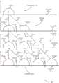
图4说明根据本文所公开的实例的支持存储器系统处的覆写的覆写方案400的实例。覆写方案400可包含分界配置401-a(例如,初始写入配置)、分界配置401-b(例如,第一覆写配置)和分界配置401-c(例如,第二覆写配置),其中的每一个可包含逻辑状态分布集415和相对于单元特性420的分界410。覆写方案400可由参考图1、2和3所描述的存储器系统110的一或多个组件实施。举例来说,存储器系统110的一或多个组件可根据用于初始编程和读取操作的分界配置401-a来操作存储器裸片160的至少一部分(例如,一或多个存储器单元205或305),确定覆写存储器裸片160的部分(例如,在不执行擦除操作的情况下),并且随后根据分界配置401-b或分界配置401-c操作存储器裸片160的部分。4 illustrates an example of an
可相对于可与存储器单元本身的物理特性相关联的单元特性420或与操作(例如,读取、写入)存储器单元相关联的物理特性来描述分界配置401中的每一个。在一些实例中,单元特性420可表示电压或电荷,例如写入到存储器单元或由存储器单元存储的电压或电荷、存储器单元的激活阈值电压(例如,VT),或由读取存储器单元产生的电压或电荷。在一些实例中,单元特性420可表示电阻或电流,例如与读取存储器单元相关联的检测到的电阻或电流。Each of
分界配置401中的每一个可与逻辑状态分布集415相关联,其中的每一个可对应于与相应逻辑状态相关联的单元特性420的值的分布。举例来说,在分界配置401-a中,逻辑状态分布415-a-1可对应于与逻辑1相关联的单元特性420的值范围,且逻辑状态分布415-a-2可对应于与逻辑0相关联的单元特性420的值范围(反之亦然)。在一些实例中,逻辑状态分布415可表示与存储器裸片160的存储器单元群相关联的不同逻辑状态。举例来说,给定逻辑状态分布415可说明当被编程有对应于给定逻辑状态分布的逻辑状态时与存储器单元群相关联的电压或电流的分布。在覆写方案400的实例中,分界配置401中的每一个包含两个逻辑状态分布415,其可对应于根据两个逻辑状态的操作。然而,分界配置401的其它实例可与不同数量的逻辑状态分布415相关联(例如,以支持例如在多层级单元覆写配置中,在大于两个逻辑状态下的覆写实施方案)。Each of
逻辑状态分布415中的每一个可与用于以对应逻辑状态编程存储器单元的相应写入操作配置(例如相应写入电压或写入电流)相关联。举例来说,在分界配置401-a中,可根据逻辑状态分布415-a-1通过施加第一写入电压或写入电流来编程存储器单元(例如,以写入逻辑1),且可根据逻辑状态分布415-a-1通过施加具有不同于第一写入电压或写入电流的值(例如,更高值、更低值)的第二写入电压或写入电流来编程存储器单元(例如,以写入逻辑0)。在各种实例中,可通过与逻辑状态分布415中的每一个相关联的单个相应写入信号或多个相应写入信号(例如,具有不同配置,例如不同量值或定时)支持此类技术。Each of
分界配置401中的每一个也可与分界410相关联,所述分界410可说明支持区分逻辑状态分布415的单元特性420的值(例如,逻辑状态之间的分界,支持一个逻辑状态和另一逻辑状态之间的评估或区分)。举例来说,分界410可说明读取分界,例如参考电压(例如,施加至控制栅极215以评估穿过存储器单元的电流的存在或不存在的参考电压,例如VTarget、相较于当读取存储器单元时的感测电压的参考电压)、参考电流,或用以评估存储器单元是被编程有与逻辑1或逻辑0相关联的单元特性420还是正在存储与逻辑1或逻辑0相关联的单元特性420的参考电阻。在覆写方案400的实例中,分界配置401中的每一个包含用于区分与两个逻辑状态相关联的两个相应逻辑状态分布415的单个分界410。然而,分界配置401的其它实例可与不同数量的分界410相关联以支持两个或更多个逻辑状态之间的其它评估,或两个或更多个逻辑状态分布415之间的评估。Each of the
覆写方案400的实例说明可由支持根据本文所公开的实例的覆写技术的存储器系统110实施的分界配置401的进程。举例来说,分界配置401-a可说明与已经擦除或先前尚未经编程的存储器单元的初始编程相关联的初始分界配置。根据分界配置401-a,可通过施加与包含在逻辑状态分布415-a-1中的存储器单元的第一逻辑状态(例如,逻辑1)相关联的第一写入信号(例如,写入电压、写入电流),或通过施加与包含在逻辑状态分布415-a-2中的存储器单元的第二逻辑状态(例如,逻辑0)相关联的第二写入信号,以此编程存储器阵列的至少一部分的存储器单元。在这类编程之后,为了评估给定存储器单元是已被编程有第一逻辑状态还是已被编程有第二逻辑状态,存储器系统110可支持根据分界410-a执行读取操作(例如,评估与正被读取的存储器单元相关联的单元特性420的值是低于分界410-a,这可指示逻辑1,还是高于分界410-a,这可指示逻辑0)。The example of an
在各种实施方案中,存储器系统110(例如,的控制器)的一部分可确定覆写根据分界配置401-a正被操作或已经操作的存储器单元,这可包含转变到根据分界配置401-b(例如,第一覆写分界配置)操作这类存储器单元。根据分界配置401-b,可通过施加与包含在逻辑状态分布415-b-1中的存储器单元的第一逻辑状态(例如,逻辑1)相关联的第一写入信号(例如,写入电压、写入电流),或通过施加与包含在逻辑状态分布415-b-2中的存储器单元的第二逻辑状态(例如,逻辑0)相关联的第二写入信号,以此编程存储器单元。在这类编程之后,为了评估给定存储器单元是已被编程有第一逻辑状态还是已被编程有第二逻辑状态,存储器系统110可支持根据分界410-b执行读取操作(例如,评估与正被读取的存储器单元相关联的单元特性420的值是低于分界410-b,这可指示逻辑1,还是高于分界410-b,这可指示逻辑0)。因此,根据分界配置401-b正被操作的存储器单元可配置为SLC存储器单元(例如,根据单个分界410经编程或配置,根据两个可能的逻辑状态中的一个经编程),且可经由单层级读取操作读取逻辑状态(例如,与单个参考电压或单个参考电流相关联的读取操作)。然而,在分界配置401-b的实例中,与相应逻辑状态分布415-b相关联的单元特性420的值范围以及分界410-b的单元特性420的值可沿着单元特性420的轴移位(例如,到更高量值)。In various embodiments, a portion of memory system 110 (eg, a controller of ) may determine to overwrite memory cells that are being or have been operated according to demarcation configuration 401-a, which may include transitioning to memory cells according to demarcation configuration 401-b Such memory cells are operated (eg, the first overwrite demarcation configuration). According to demarcation configuration 401-b, a first write signal (eg, write voltage , write current), or by applying a second write signal associated with a second logic state (eg, logic 0) of the memory cells included in the logic state distribution 415-b-2, thereby programming the memory cells. After such programming, in order to evaluate whether a given memory cell has been programmed with a first logic state or a second logic state, memory system 110 may support performing a read operation according to demarcation 410-b (e.g., evaluating with Whether the value of the cell characteristic 420 associated with the memory cell being read is below the demarcation 410-b, which may indicate a
在一些实施方案中,根据分界配置401-b的存储器单元覆写可支持将信息写入(例如,覆写)到存储器阵列的先前被写入的部分,但无需中介擦除操作。举例来说,因为逻辑状态分布415-b-2与单元特性的不与逻辑状态分布415-a-1或逻辑状态分布415-a-2重叠的值范围相关联,所以逻辑状态分布415-b-2可为可与单元特性420的与逻辑状态分布415-a-1和415-a-2相关联的那些值区分开(例如,根据分界410-b)。在NAND存储器架构中,举例来说,当覆写分界配置401(例如,分界配置401-b和401-c的两个或更多个逻辑状态分布415中的每一个)具有单元特性420的大于或等于逻辑状态分布415或前一分界配置(例如,不低于前一分界配置401(例如分界配置401-a)的那些范围)的相应范围时可支持此类技术。In some implementations, memory cell overwriting according to demarcation configuration 401-b can support writing (eg, overwriting) information to previously written portions of the memory array without an intervening erase operation. For example, because logical state distribution 415-b-2 is associated with a range of values for cell characteristics that do not overlap logical state distribution 415-a-1 or logical state distribution 415-a-2, logical state distribution 415-b -2 may be distinguishable from those values of cell characteristic 420 associated with logic state distributions 415-a-1 and 415-a-2 (eg, according to demarcation 410-b). In a NAND memory architecture, for example, when overwriting demarcation configuration 401 (e.g., each of two or more
在一些实施方案中,与逻辑状态分布415-b-2相关联的量值大于与逻辑状态分布415-a-2相关联的写入信号(例如,更高电压、更高电流)的写入信号可支持这类转变。在各种实例中,逻辑状态分布415-b-1可具有单元特性420的与逻辑状态分布415-a-2的范围值相同、部分地重叠或至少部分地大于或等于(例如,不低于)所述范围值的范围值。举例来说,与逻辑状态分布415-b-1相关联的写入信号可具有等于或大于与逻辑状态分布415-a-2相关联的写入信号的量值。因此,在一些实例中,可能没有正在根据单元特性420的先前与分界配置401-a的逻辑状态分布415-a-1相关联的范围值被写入的存储器单元与分界配置401-b相关联。In some embodiments, the magnitude associated with logic state distribution 415-b-2 is greater than the write signal (e.g., higher voltage, higher current) associated with logic state distribution 415-a-2. Signals support such transitions. In various examples, logical state distribution 415-b-1 may have the same range of values for cell characteristic 420 as logical state distribution 415-a-2, partially overlap, or be at least partially greater than or equal to (e.g., not less than ) the range value of the range value. For example, a write signal associated with logic state distribution 415-b-1 may have a magnitude equal to or greater than a write signal associated with logic state distribution 415-a-2. Thus, in some instances, there may be no memory cells that are being written to range values of
在一些实例中,根据一些分界配置401(例如,分界配置401-a)的操作可涉及与其它分界配置(例如,分界配置401-b或401-c)相比相对较低的编程应力,这可与关联于这类分界配置401的写入信令的相对较低量值有关。因此,覆写方案400的实例可说明在具有减小的容限的SLC覆写模式中操作存储器阵列的一部分的实例(例如,相较于与对应于一个逻辑状态的逻辑状态分布415-a-1和对应于另一逻辑状态的逻辑状态分布415-b-2相关联的容限),这可降低存储器单元疲乏。通过支持在达到编程应力的最高配置水平(例如,与分界配置401-c相关联)之前在一些分界配置中在较低编程应力下被写入的数据,存储器单元可支持在达到最高配置编程应力和后一擦除操作之前被写入相对较高数量的新信息(例如,根据分界配置401-a、401-b和401-c序列),这可支持用于相关联存储器装置的TBW的较高额定值。In some examples, operation according to some demarcation configurations 401 (e.g., demarcation configuration 401-a) may involve relatively lower programming stress compared to other demarcation configurations (e.g., demarcation configurations 401-b or 401-c), which This may be related to the relatively low magnitude of write signaling associated with
逻辑状态向逻辑状态分布415-b-1和415-b-2的指配可根据各种技术配置,包含可与分界配置401-a中的逻辑状态的指配有关的这类指配。举例来说,在维持相对于分界410的定位的配置中,小于分界410的逻辑状态分布415可与一个逻辑状态相关联(例如,其中逻辑状态分布415-a-1和415-b-1各自与逻辑1相关联),且大于分界410的逻辑状态分布415可与另一逻辑状态相关联(例如,其中逻辑状态分布415-a-2和415-b-2与逻辑0相关联)。在另一实例中,在维持用于单元特性420的范围值的逻辑状态的配置(例如,其中逻辑状态分布415-a-2和415-b-1大体上共同延伸,或在阈值内共同延伸)中,逻辑状态分布415-a-2和415-b-1可各自与逻辑0相关联,且逻辑状态分布415-a-1和415-b-1可各自与逻辑1相关联。在一些实例中,存储器系统可支持这类指配的动态选择,例如从一个分界配置401到另一分界配置401的选择,使在相对较高写入信令下被写入的存储器单元的数量降到最低,或使在一般情况下被写入的存储器单元的数量降到最低,以及其它准则,可在页层级、块层级或平面层级以及其它粒度上进行评估。The assignment of logical states to logical state distributions 415-b-1 and 415-b-2 may be configured according to various techniques, including such assignments that may be related to the assignment of logical states in demarcation configuration 401-a. For example, in configurations where positioning relative to
在一些实例中,通过维持每一分界配置401的单个分界410,覆写方案400可支持以相对更快速或更低复杂性感测方案或电路系统进行覆写。举例来说,覆写方案400可支持与其它SLC配置相同或类似读取带宽,包含SLC配置或用于可不被配置成支持覆写技术的单层级读取操作的其它技术。In some examples, by maintaining a
存储器系统110可支持根据覆写方案400的实例的任何数量的一或多个覆写分界配置401。举例来说,在支持第二覆写分界配置的配置中,存储器系统110的一部分可确定覆写正在或已经根据分界配置401-b进行操作的存储器单元,所述操作可包含根据分界配置401-c操作这类存储器单元。根据分界配置401-c,可通过施加与包含在逻辑状态分布415-c-1中的存储器单元的第一逻辑状态(例如,逻辑1)相关联的第一写入信号,或通过施加与包含在逻辑状态分布415-c-2中的存储器单元的第二逻辑状态(例如,逻辑0)相关联的第二写入信号,以此编程存储器单元。在这类编程之后,为了评估给定存储器单元是在第一逻辑状态下还是在第二逻辑状态下已被编程,存储器系统110可支持根据分界410-c执行读取操作(例如,评估正被读取的存储器单元的单元特性420的值是低于分界410-c,这可指示逻辑1,还是高于分界410-c,这可指示逻辑0)。在一些情况下,存储器系统110可利用检查失败字节跟踪用于每一连续写入(例如,以确保在连续覆写之后的存取操作的准确性)。Memory system 110 may support any number of one or more
在一些实例中,根据连续覆写写入存储器单元(例如,根据分界配置401-b和401-c的编程操作)的持续时间可增加。举例来说,写入信号量值增加可涉及达到较高电压的更长持续时间,或较高存储电荷,或调用存储器单元的物理改变的更长时间,以及其它现象。因此,用于执行编程操作的配置持续时间可针对不同的分界配置401增加,或以其它方式改变。In some examples, the duration of writing to memory cells according to successive overwrites (eg, programming operations according to demarcation configurations 401-b and 401-c) can increase. For example, an increase in write signal magnitude may relate to a longer duration of reaching a higher voltage, or a higher stored charge, or a longer time to invoke a physical change of the memory cell, among other phenomena. Accordingly, configuration durations for performing programming operations may be increased for
在一些实例中,从一个分界配置401另一分界配置401的分界410之间的单元特性420的差异,或从一个分界配置401到另一分界配置401的最高逻辑状态分布415之间的差异可被视为阶跃(例如,电压阶跃)。在一些情况下,这类阶跃可被配置为相对小,这可与避免关联于将数据写入到存储器单元的阈值(例如,电压阈值)的超越相关联。此外,通过实施连续分界配置401之间的小阶跃,存储器系统110可支持在不超过这类阈值的情况下更大数量的分界配置401(例如,更大数量的覆写)。In some examples, the difference in
在一些实例中,存储器的支持覆写方案400等等的部分可为可根据覆写方案和另一多层级单元配置操作的。举例来说,存储器阵列的可支持根据四个逻辑状态分布415的操作的部分和这类逻辑状态分布415可与(例如,静态地、动态地)在给定时间在其中四个逻辑状态分布415中的每一个可存储四个逻辑状态(例如,逻辑00、逻辑01、逻辑10或逻辑11)中的一个的MLC配置中,或在其中对于每一分界配置401,两个逻辑状态分布415可用于支持逻辑0和逻辑1的SLC覆写配置中操作相关联。举例来说,在覆写方案400的逻辑状态分布415的上下文中,可当逻辑状态分布415-a对应于逻辑00,逻辑状态分布415-a-2和415-b-1对应于逻辑01,逻辑状态分布415-b-2和415-c-1对应于逻辑10,且逻辑状态分布415-c-2对应于逻辑11,以及其它关联性时支持MLC配置。在一些此类实例中,分界410-a、410-b和410-c可与支持MLC操作的多层级读取操作或电路系统相关联,且在一些实例中,这类操作或电路系统可在当在覆写方案(例如,SLC覆写方案,与一次使用单个分界410有关)中操作时功率消耗减小或读取带宽增加下操作。In some examples, portions of memory that support the
在一些实例中,可存储器系统110可在确定如何配置或操作存储器装置130的这类部分时考虑这类条件。举例来说,存储器系统110可确定针对相对较高容量、针对较不可能被替换的信息、针对其中读取带宽相对较不重要的信息或操作条件,或针对其中与编程和擦除操作相关联的应力相对较不重要的条件,在MLC模式中操作。在一些实例中,存储器系统110可确定针对更有可能被替换的信息(例如,L2P表、写入助推器缓冲器、奇偶数据)、针对其中读取带宽相对更重要的信息或操作条件,或针对其中与编程和擦除操作相关联的应力相对更重要的条件,在SLC覆写模式或其它覆写模式中操作。在一些实例中,存储器系统110可动态地(例如,基于当前操作条件)做出这类确定,或存储器系统110可配置存储器装置130的某些部分在MLC模式中操作,且存储器装置130的特定其它部分或另一存储器装置130在覆写模式中操作。虽然在四个逻辑状态分布415的上下文中进行描述,且在MLC模式和SLC分界配置401之间进行权衡,但此类技术可应用于任何数量的逻辑状态分布415和多层级写入配置(例如,TLC写入配置、QLC写入配置)和覆写配置(例如,SLC覆写配置、多层级覆写配置)的各种实施方案。In some examples, memory system 110 may consider such conditions when determining how to configure or operate such portions of memory device 130 . For example, memory system 110 may determine that for relatively higher capacities, for information that is less likely to be replaced, for information or operating conditions where read bandwidth is relatively less important, or for information that is associated with program and erase operations Conditions of stress are relatively unimportant to operate in MLC mode. In some examples, memory system 110 may determine that for information that is more likely to be replaced (e.g., L2P tables, write booster buffers, parity data), for information or operating conditions where read bandwidth is relatively more important, Or operate in SLC overwrite mode or other overwrite modes for conditions where the stress associated with program and erase operations is relatively more important. In some examples, memory system 110 may make such determinations dynamically (e.g., based on current operating conditions), or memory system 110 may configure certain portions of memory device 130 to operate in MLC mode, with specific portions of memory device 130 Other portions or another memory device 130 operates in an overwrite mode. Although described in the context of four
在一些情况下,存取操作信令(例如,读取操作信令或写入操作信令、存储器系统控制器115和存储器装置130之间的命令信令)可指示分界配置401,或其分界410(例如,参考电压的指示)。举例来说,命令信令可根据特定分界配置401或分界410引导存储器装置130将逻辑状态写入到存储器单元,或根据特定分界配置401或分界410从存储器单元读取逻辑状态。在一些实例中,分界配置401可受存储器装置130(例如,受本地控制器135)管理,在此情况下,存取操作信令可忽略分界的指示。举例来说,存储器装置130(例如,本地控制器135)可确定用新信息覆写存储器的一部分,可与从一个分界配置401到另一分界配置401的转变(例如,在存储器装置处确定)相关联。In some cases, access operation signaling (e.g., read or write operation signaling, command signaling between memory system controller 115 and memory device 130) may indicate
在一些情况下,存储器系统110的组件(例如,存储器系统控制器115、本地控制器135)可跟踪覆写数量,或分界配置401或其分界410,以确定在未来覆写中使用哪个分界配置401。举例来说,可在存储器系统110的组件中的存储器阵列的每部分(例如,每块、每页)存储用于读取偏移的多个模式(例如,A/B/C模式)。在一些情况下,存储器系统110处的固件可跟踪存储于系统中的读取偏移。覆写方案400可使得存储器装置130能够节约一定数量的擦除循环(例如,存储器装置130可以不为了将新数据写入到所述单元而擦除或执行垃圾收集),或可减小单层级单元编程-擦除周期需求,以及其它益处。In some cases, components of memory system 110 (e.g., memory system controller 115, local controller 135) may track the number of overwrites, or
图5说明根据本文所公开的实例的支持存储器系统处的覆写的覆写方案500的实例。覆写方案500可包含经擦除状态505,其中在一些情况下,经擦除存储器单元可被视为存储逻辑1(例如,与逻辑状态分布415-d内的单元特性420-a相关联)。覆写方案500还可包含分界配置401-d(例如,初始写入配置)、401-e(例如,第一覆写配置)和401-f(例如,第二覆写配置)。覆写方案500可由参考图1、2和3所描述的存储器系统110的一或多个组件实施。5 illustrates an example of an
在覆写方案500的实例中,可与单元特性420-a相关地描述分界配置401中的每一个,所述单元特性420-a可为参考图4所描述的单元特性420的实例。分界配置401中的每一个也可与相应逻辑状态分布集415相关联,所述相应逻辑状态分布集415中的每一个可对应于单元特性420-a的与相应逻辑状态相关联的值的分布,且所述相应逻辑状态分布集415中的每一个可与用于在对应逻辑状态下编程存储器单元的相应写入操作配置相关联。分界配置401中的每一个也可与一或多个分界410相关联,其可说明单元特性420-a的支持区分开逻辑状态分布415的值。In the example of the
覆写方案500的实例说明可由存储器系统110实施的支持根据本文所公开的实例的覆写技术的分界配置401的另一进程。举例来说,当执行覆写操作时,一个分界配置401和另一分界配置401之间的转变可涉及存储器阵列的一部分的存储器单元上的一或多个保存操作510(例如,保存单元特性420-a的值,保存逻辑状态)、存储器阵列的部分的存储器单元上的一或多个翻转操作515(例如,改变单元特性420-a的值,翻转逻辑状态),或其各种组合。在一些实例中,这类转变可涉及评估给定存储器单元的所存储的状态(例如,逻辑状态、单元特性420-a的值)以确定是执行保存操作510还是翻转操作515。举例来说,对于存储器的正被覆写的部分的每一存储器单元,存储器系统110(例如,存储器装置130、本地控制器135)可评估是保存存储于存储器单元处的逻辑状态或单元特性420-a,还是改变存储于存储器单元处的单元特性420-a的逻辑状态。在各种实例中,可对存储器阵列的被标记为存储无效数据的部分执行这类操作,且这类操作随后可将存储器阵列的所述部分标记为存储有效数据而不管是否施加写入信号。The example of
在一些实例中,对于存储器阵列的与经擦除状态505相关联的部分,全部存储器单元可在一开始与逻辑状态分布415-d相关联,所述逻辑状态分布415-d可与逻辑1(例如,第一逻辑状态)相关联。为了根据分界配置401-d编程存储器单元,存储器装置130可执行保存操作510-a以将存储器单元确立为存储逻辑1(例如,第一逻辑状态),或执行翻转操作515-a以将存储器单元确立为存储逻辑0(例如,第二逻辑状态)。在一些实例中,保存操作510-a可与施加第一写入信号(例如,与保存操作510-a或逻辑状态分布415-e-1相关联的写入电压或写入电流、刷新信号)相关联,且翻转操作515-a可与施加第二写入信号(例如,与翻转操作515-a或逻辑状态分布415-e-2相关联的写入电压或写入电流)相关联。在一些实例中,保存操作510-a可与将空或零偏压施加到存储器单元相关联,或可与制止将写入信号施加到存储器单元相关联,进而维持单元特性420-a或已经编程到存储器单元的逻辑状态。In some examples, for the portion of the memory array associated with the erased state 505, all memory cells may initially be associated with a logic state distribution 415-d, which may be associated with a logic 1 ( For example, the first logical state) is associated. To program a memory cell according to demarcation configuration 401-d, memory device 130 may perform a save operation 510-a to establish the memory cell as storing a logical 1 (e.g., a first logic state), or perform a flip operation 515-a to restore the memory cell to Established to store a logic zero (eg, second logic state). In some examples, save operation 510-a may be associated with applying a first write signal (e.g., write voltage or write current, refresh signal associated with save operation 510-a or logic state distribution 415-e-1) associated, and flip operation 515-a may be associated with applying a second write signal (eg, the write voltage or write current associated with flip operation 515-a or logic state distribution 415-e-2). In some examples, save operation 510-a may be associated with applying a null or zero bias voltage to the memory cell, or may be associated with refraining from applying a write signal to the memory cell, thereby maintaining cell characteristic 420-a or programmed to the logic state of the memory cell.
在一些实例中,可在不针对所存储逻辑状态或单元特性420-a评估存储器单元的情况下(例如,在执行保存操作510-a或翻转操作515-a之前),例如当对存储器阵列的部分已经擦除的指示与存储器单元处于已知状态相关联时,执行从经擦除状态505到分界配置401-d的转变。换句话说,对目标存储器单元是执行保存操作510-a还是翻转操作515-a的确定可基于将写入到目标存储器单元的逻辑状态,并且可独立于目标状态存储器单元的当前状态。在对存储器阵列的一部分的相应存储器单元执行保存操作510-a或翻转操作515-a之后,存储器阵列的所述部分可根据分界配置401-d存储数据。为了评估给定存储器单元是已经被编程有逻辑1还是逻辑0,存储器系统110可支持根据分界410-d的读取操作(例如,评估单元特性420-a的值是低于分界410-d,这可指示逻辑1,还是高于分界410-d,这可指示逻辑0)。In some examples, memory cells may be evaluated without evaluating the stored logic state or cell characteristic 420-a (eg, prior to performing the save operation 510-a or flip operation 515-a), such as when the memory array's The transition from erased state 505 to demarcated configuration 401-d is performed when the indication that a portion has been erased is associated with the memory cell being in a known state. In other words, the determination of whether to perform save operation 510-a or flip operation 515-a on a target memory cell may be based on the logical state to be written to the target memory cell and may be independent of the current state of the target state memory cell. After performing a save operation 510-a or a flip operation 515-a on corresponding memory cells of a portion of the memory array, the portion of the memory array may store data according to the demarcation configuration 401-d. To assess whether a given memory cell has been programmed with a logical 1 or a logical 0, memory system 110 may support read operations according to demarcation 410-d (e.g., evaluating whether the value of cell characteristic 420-a is below demarcation 410-d, This may indicate a logical 1, or above the demarcation 410-d, which may indicate a logical 0).
在各种实施方案中,存储器系统110的一部分可确定覆写存储器阵列的已经根据分界配置401-d操作的部分,所述操作可包含根据分界配置401-e(例如,第一覆写分界配置)操作这类存储器单元。在一些实例中,存储器单元的评估可支持从分界配置401-d到分界配置401-e的覆写转变以确定是执行保存操作510还是翻转操作515。In various embodiments, a portion of memory system 110 may determine to overwrite portions of the memory array that are already operating according to demarcation configuration 401-d, which may include operating according to demarcation configuration 401-e (e.g., the first overwrite demarcation configuration ) to operate such memory cells. In some examples, evaluation of memory cells may support an overwrite transition from demarcation configuration 401 - d to demarcation configuration 401 - e to determine whether to perform save
举例来说,为了将存储器单元确立为存储逻辑1,但可首先在读取或其它感测操作中评估存储器单元以确定存储器单元的单元特性420-a的当前逻辑状态或值。如果存储器单元与单元特性420-a的对应于逻辑状态分布415-e-1的逻辑状态或值相关联,那么可执行保存操作510-b以使得单元特性420-a的与写入的存储器单元相关联的值处于逻辑状态分布415-f-1内。保存操作510-b可与施加第一写入信号相关联,或可与制止将写入信号施加到存储器单元相关联。如果存储器单元与单元特性420-a的对应于逻辑状态分布415-e-2的逻辑状态或值相关联,那么可执行翻转操作515-c以使得单元特性420-a的与写入的存储器单元相关联的值处于逻辑状态分布415-f-3内,这说明第二逻辑状态分布415(例如,多个逻辑状态分布415)对应于逻辑1。翻转操作515-c可与施加第三写入信号(例如,与翻转操作515-c或逻辑状态分布415-f-3相关联的写入电压或写入电流)相关联,所述第三写入信号与第一写入信号和第二写入信号二者相比可具有更高量值。For example, to establish a memory cell as storing a logical one, the memory cell may first be evaluated in a read or other sensing operation to determine the current logic state or value of the memory cell's cell characteristic 420-a. If a memory cell is associated with a logic state or value of cell characteristic 420-a corresponding to logic state distribution 415-e-1, save operation 510-b may be performed such that the memory cell of cell characteristic 420-a is associated with the written memory cell The associated values are within the logical state distribution 415-f-1. The save operation 510-b may be associated with applying the first write signal, or may be associated with refraining from applying the write signal to the memory cell. If a memory cell is associated with a logic state or value of cell characteristic 420-a that corresponds to logic state distribution 415-e-2, flip operation 515-c may be performed such that the cell characteristic 420-a is consistent with the written memory cell The associated value is within logical state distribution 415-f-3, which indicates that the second logical state distribution 415 (eg, plurality of logical state distributions 415) corresponds to a logical one. Flip operation 515-c may be associated with applying a third write signal (e.g., a write voltage or write current associated with flip operation 515-c or logic state distribution 415-f-3) that The IN signal may have a higher magnitude than both the first write signal and the second write signal.
在一些实例中,为了将存储器单元确立为存储逻辑0,也可首先在读取或其它感测操作中评估存储器单元以确定存储器单元的单元特性420-a的当前逻辑状态或值。如果存储器单元与单元特性420-a的对应于逻辑状态分布415-e-1的逻辑状态或值相关联,那么可执行翻转操作515-b以使得单元特性420-a的与写入的存储器单元相关联的值处于逻辑状态分布415-f-2内。在一些实施方案中,翻转操作515-b可例如当逻辑状态分布415-e-2和415-f-2大体上共同延伸或在阈值内共同延伸时,与施加第二写入信号相关联。如果存储器单元与单元特性420-a的对应于逻辑状态分布415-e-2的逻辑状态或值相关联,那么可执行保存操作510-c以使得单元特性420-a的与写入的存储器单元相关联的值处于逻辑状态分布415-f-2内。翻转操作515-c也可与施加第二写入信号相关联,或可与制止将写入信号施加到存储器单元相关联。在一些实例中,由于逻辑状态分布415-f-2可与第二写入信号相关联而与存储器单元的前一状态无关,因此可在不评估待写入存储器单元的情况下执行在到分界配置401-e的覆写转变中编程逻辑0的操作。In some examples, to establish a memory cell as storing a logical zero, the memory cell may also first be evaluated in a read or other sensing operation to determine the current logic state or value of the memory cell's cell characteristic 420-a. If a memory cell is associated with a logic state or value of cell characteristic 420-a that corresponds to logic state distribution 415-e-1, flip operation 515-b may be performed such that the memory cell of cell characteristic 420-a is consistent with the written memory cell The associated values are within the logical state distribution 415-f-2. In some implementations, flipping operation 515-b may be associated with applying a second write signal, eg, when logic state distributions 415-e-2 and 415-f-2 are substantially coextensive or coextensive within a threshold. If a memory cell is associated with a logic state or value of cell characteristic 420-a corresponding to logic state distribution 415-e-2, save operation 510-c may be performed such that the memory cell of cell characteristic 420-a is associated with the written memory cell The associated values are within the logical state distribution 415-f-2. Flip operation 515-c may also be associated with applying the second write signal, or may be associated with refraining from applying the write signal to the memory cell. In some examples, since the logic state distribution 415-f-2 can be associated with the second write signal regardless of the previous state of the memory cell, it may be performed without evaluating the memory cell to be written. The operation of
在执行保存操作510-b或510-c或翻转操作515-b或515-c之后,存储器阵列的部分可根据分界配置401-e存储数据。为了评估给定存储器单元是已经被编程有逻辑1还是逻辑0,存储器系统110可支持根据分界410-e-1和410-e-2的读取操作,这说明针对给定数量的逻辑状态(例如,两个逻辑状态)分界410的数量增加(例如,两个分界410)的实例。在一些实例中,每一分界410-e可与相应读取操作(例如,多个单层级读取,例如当分界410-e说明施加至控制栅极215的参考电压时)相关联。如果存储器系统110确定(例如,在一个读取评估中)存储器单元的单元特性420-a的值低于分界410-e-1,那么存储器系统110可确定存储器单元处于逻辑状态分布415-f-1内(例如,与逻辑状态1相关联)。如果存储器系统110确定存储器单元的单元特性420-a的值高于分界410-e-1,那么根据分界410-e-2的读取评估可支持逻辑状态评估。如果存储器系统110确定存储器单元的单元特性420-a的值低于分界410-e-2,那么存储器系统110可确定存储器单元处于逻辑状态分布415-f-2内(例如,与逻辑状态0相关联),且如果存储器系统110确定存储器单元的单元特性420-a的值高于分界410-e-2,那么存储器系统110可确定存储器单元处于逻辑状态分布415-f-3内(例如,与逻辑状态1相关联)。虽然在不同操作的上下文中进行描述,但在一些实例中,分界410-e-1和410-e-2可与多层级读取操作或感测电路系统的层级相关联。After performing a save operation 510-b or 510-c or a flip operation 515-b or 515-c, the portion of the memory array may store data according to the demarcation configuration 401-e. To assess whether a given memory cell has been programmed with a logical 1 or a logical 0, the memory system 110 may support read operations according to boundaries 410-e-1 and 410-e-2, which indicate that for a given number of logical states ( For example, two logical states) instances of the
存储器系统110可支持根据覆写方案500的实例的任何数量的一或多个覆写分界配置401。举例来说,在支持第二覆写分界配置的配置中,存储器系统110的一部分可确定覆写存储器阵列的已经根据分界配置401-e操作的部分,所述操作可包含根据分界配置401-f操作存储器阵列的部分。如所说明,各种保存操作510和翻转操作515可支持从分界配置401-e到分界配置401-f的转变,在根据本文所公开的实例的这类操作之前对存储器单元的评估可支持这类操作。在执行这类操作之后,存储器阵列的部分可根据分界配置401-f存储数据。为了评估给定存储器单元是已经被编程有逻辑1还是逻辑0,存储器系统110可支持根据分界410-f-1、410-f-2和410-f-3的读取操作,可通过各种单层级或多层级技术执行所述读取操作。Memory system 110 may support any number of one or more
根据覆写方案500的存储器单元覆写说明将信息写入(例如,覆写)到存储器的先前被写入的部分但无需中介擦除操作的另一实例。举例来说,为了支持在覆写方案500中从一个分界配置401到另一分界配置401的转变,存储器装置130可确定是通过翻转操作515覆写存储器单元还是通过保存操作510保存先前写入的状态。在一些实例中,根据覆写方案500的这类操作可减小施加至存储器单元的写入信号的数量,或减小写入到存储器单元的写入信号的量值,这可减小存储器单元的功率消耗或降级,以及其它优点。虽然此类技术与(例如,与分界配置401-e和401-f中的多层级读取的实施方案有关的)覆写方案相比可与相对较慢读取带宽相关联,但写入操作的发生率和量值减小可与对存储器装置的循环疲乏、单元降级和整体操作寿命的改进(例如,更大TBW、更高编程/擦除耐久性)相关联。Memory cell overwriting according to overwriting
虽然覆写方案500的实例说明其中逻辑状态维持在单元特性420-a的相应范围内的技术,但在一些实例中,可通过连续覆写翻转对应于单元特性420-a的相应范围的逻辑状态。在一些实例中,可基于可维持于给定状态中的单元比例例如保存操作510和翻转操作515的比较来确定这类逻辑状态指配,所述比较将引起一个逻辑状态指配对比另一逻辑状态指配。此外,类似于覆写方案400的实例,覆写方案500的逻辑状态分布415中的每一个可与另一多层级单元模式(例如,MLC、TLC或QLC模式)相关联或以其它方式可配置有所述另一多层级单元模式,且存储器系统110或存储器装置130可被配置成取决于各种各个因素或操作条件确定是否根据覆写方案500的一或多个方面操作。While the example of
在一些实施方案中,存储器系统110可被配置成支持覆写方案400和覆写方案500两者的方面等等,且存储器系统110可被配置成取决于存储器装置130或其部分(例如,针对存储器阵列的一个部分对比另一部分)的性能权衡根据彼此的差异进行操作。在一些实例中,可针对与每一分界配置401的单个或者一致数量的分界410相关联的相对低时延来选择覆写方案400的方面。在一些实例中,可针对与省略写入操作的可能性相关联的相对低功率消耗或相对低疲乏或降级或针对执行相对较低量值写入操作来选择覆写方案500的方面,而不考虑相对更复杂的读取操作。在一些实例中,存储器阵列的每一部分可通过覆写技术的启用或停用进行配置,或通过特定覆写方案或其配置进行配置,其可对应于给定存储器装置130的实施方案的类型,或存储于存储器装置130处的信息的优先级或其它特性,这类特性可适应此类配置的各种粒度。在一些实例中,可针对特定类型的信息,或与特定类型的信息相关联的物理分配(例如L2P表、奇偶校验信息或其它相对瞬态数据)确定或配置此类技术。在一些实例中,此类技术可与“原位”垃圾收集相关联,这可避免与这类垃圾收集相关联的擦除操作。在一些实例中,这类确定可基于相关联固件复杂性、读取干扰的相对倾向、相关联原始位错误率(RBER)、读取带宽或时延或助推器缓冲器可用性以及其它考虑因素。In some embodiments, memory system 110 may be configured to support aspects of both overwrite
图6A说明根据本文所公开的实例的支持存储器系统处的覆写的过程流600的实例。过程流600可由参考图1-3所描述的存储器系统110的一或多个组件实施。举例来说,过程流600的方面可由存储器系统控制器115-a和存储器装置130-c执行或在其间执行。6A illustrates an example of a
在625处,存储器系统(例如,存储器装置130-c)可执行写入操作以将第一信息存储于(例如,存储器装置130-c的)存储器阵列的一部分处。可根据第一分界(例如,第一电压分界、第一分界配置401)执行写入操作。在一些实例中,可根据初始分界配置401或随后可被覆写的中等覆写分界配置401执行625的写入操作。写入第一信息可与单元特性420的关联于写入的逻辑状态的第一写入信令或值集(例如,电压、电流、电阻)相关联。625处的写入可与逻辑状态数量(例如在SLC操作模式中的两个逻辑状态)相关联,且在一些实例中,针对存储器阵列的(例如,可为可在MLC模式、TLC模式或QLC模式等等中操作的)部分,逻辑状态的数量可少于逻辑状态的总可操作数量。625的写入操作可响应于从主机系统105接收的写入命令,或可与存储器管理操作(例如耗损均衡或垃圾收集以及其它实例)相关联。在各种实例中,625的执行写入操作可与存储器系统控制器115-a或存储器装置130-c存储在存储器阵列的部分处执行的覆写数量的指示,或对根据特定分界配置401或其分界410写入存储器阵列的部分的指示相关联。在一些实例中(例如,当响应于来自存储器系统控制器115-a的信令执行625的写入操作时),625的写入操作可为存储器系统控制器115-a根据覆写分界配置401执行写入操作或其至少一部分的实例。在一些实例中,可对通过覆写方案(例如,覆写方案400或500)分配的存储器的一部分执行这类写入操作,或存储器系统控制器115-a或存储器装置130-c可确定在625处以支持后一覆写的方式执行写入操作,所述方式可基于信息的类型,或所要操作或执行条件(例如,写入带宽、读取带宽、降级配置)以及其它考虑因素。At 625, the memory system (eg, memory device 130-c) may perform a write operation to store the first information at a portion of the memory array (eg, of memory device 130-c). The write operation may be performed according to a first demarcation (eg, first voltage demarcation, first demarcation configuration 401 ). In some examples, the write operation of 625 may be performed according to the
在630处,在一些实例中,存储器系统(例如,存储器系统控制器115-a)可确定覆写存储器阵列的部分。在一些实例中,这类覆写确定可基于与存储器阵列的部分相关联的有效性指示(例如,对存储于存储器阵列的部分处的数据无效或不再需要的指示)。在一些实例中,覆写存储器阵列的部分的确定可与存储于存储器阵列的部分处或将写入到存储器阵列的部分的信息的类型,或与阵列本身的部分相关联的配置(例如,针对存储器阵列的部分启用覆写的指示)相关联。举例来说,如果存储器阵列的部分与相对瞬态数据(例如,写入助推信息、奇偶校验信息、L2P地址信息)相关联,那么存储器系统控制器115-a可做出覆写已存储于存储器阵列的部分处但尚未被擦除的信息的确定(例如,而非并非执行擦除操作并且用相对非瞬态数据写入存储器阵列的部分)。在一些实例中,存储器系统控制器115-a可确定存储器阵列的部分可用于被覆写(例如,具有可用分界配置401)。在一些实例中,例如当在存储器装置130-c处(例如,响应于接收到写入操作信令)做出是否覆写存储器阵列的一部分的确定时,可省略630的操作。At 630, in some examples, the memory system (eg, memory system controller 115-a) may determine to overwrite a portion of the memory array. In some examples, such overwrite determinations may be based on indications of validity associated with portions of the memory array (eg, an indication that data stored at the portion of the memory array is invalid or no longer needed). In some examples, the determination to overwrite a portion of the memory array may be related to the type of information stored at or to be written to the portion of the memory array, or to the configuration associated with the portion of the array itself (e.g., for Indicates that a portion of the memory array enables overwriting) is associated. For example, if a portion of the memory array is associated with relatively transient data (e.g., write boost information, parity information, L2P address information), the memory system controller 115-a may make an overwrite of the stored Determination of information that is at a portion of the memory array that has not been erased (eg, rather than performing an erase operation and writing to the portion of the memory array with relatively non-transitory data). In some examples, the memory system controller 115-a may determine that a portion of the memory array is available to be overwritten (eg, has an available demarcation configuration 401). In some instances, the operation of 630 may be omitted, such as when a determination is made at memory device 130-c (eg, in response to receiving write operation signaling) whether to overwrite a portion of the memory array.
在635处,存储器系统控制器115-a可将写入操作信令(例如,将第二信息写入到存储器装置130-c的存储器阵列的部分的信令)发射到存储器装置130-c。635的写入操作信令可与根据第二分界配置401用第二信息覆写相关联。因此,写入第二信息可与单元特性420的关联于写入的逻辑状态的第二写入信令或值集(例如,电压、电流、电阻)相关联。在一些实例中,635的写入操作信令可包含第二信息和对存储器的一部分处的写入的指示(例如,逻辑地址、物理地址)。在一些情况下(例如,当存储器系统控制器115-a管理针对存储器装置130-a的地址的覆写状态时),635的写入操作信令可指示分界配置401,或其分界410,或与存储器阵列的部分相关联(例如,对其执行)的覆写数量(例如,作为与用于写入第二信息的写入配置相关联的写入操作信令的前缀、算法限定词前缀)。635的写入操作信令可响应于从主机系统105接收的写入命令,或可与可受存储器系统控制器115-a管理的存储器管理操作(例如耗损均衡或垃圾收集)相关联,以及其它实例。在一些实例中,635的写入操作信令的发射可为存储器系统控制器115-a根据覆写分界配置401执行写入操作或其至少一部分的实例。At 635, the memory system controller 115-a may transmit write operation signaling (eg, signaling to write the second information to the portion of the memory array of the memory device 130-c) to the memory device 130-c. The write operation signaling of 635 may be associated with overwriting with the second information according to the
在一些实例中,在640处,存储器装置130-c可确定用于写入第二信息的分界(例如,电压分界、分界410、分界配置401、第二分界)。在一些实例中,确定的分界可关联于与对第一信息写入的逻辑状态相同数量的逻辑状态(例如,维持SLC操作或某一其它多层级单元操作),但可与不同写入信号量值,或不同分界数量410,以及其它差异相关联。在一些情况下,存储器装置130-c可基于635的写入操作信令的指示确定用于写入第二信息的分界。在一些实例中,存储器装置130-c可基于如存储于存储器装置130-c处的覆写状态或对存储器阵列的部分执行的覆写数量的指示,确定用于写入第二信息的分界。In some examples, at 640, memory device 130-c may determine a demarcation (eg, voltage demarcation,
在645处,存储器装置130-c可执行写入操作以存储第二信息(例如,基于635的写入操作信令),这可根据在640处通过存储器装置130-c确定的分界来执行。645处执行的写入操作可与不同于625处执行的写入操作的分界配置401相关联。举例来说,与645的写入操作相关联的分界配置401可具有不同写入信令,例如用于写入给定逻辑状态的不同电压或电流,或可对应于给定逻辑状态的不同数量的写入信号。在一些实例中,645的写入操作可与具有单元特性420的不同值(例如,不同参考电压)以用于将一个逻辑状态与另一逻辑状态区分开的分界410,或不同数量的逻辑状态分布415或分界410相关联。然而,在一些实例中,645的写入操作和625的写入操作可与根据同一数量的逻辑状态(例如,同一数量的两个或更多个可能逻辑状态)的写入相关联。在一些实例中,可在625的写入操作之后不执行擦除操作的情况下执行645的写入操作。在一些情况下,在执行第二写入操作之后,存储器装置130-c可存储对已根据第二分界配置写入存储器的部分的指示。At 645, the memory device 130-c may perform a write operation to store the second information (eg, based on the write operation signaling of 635), which may be performed according to the demarcation determined at 640 by the memory device 130-c. The write operation performed at 645 may be associated with a
在一些实例中,645的写入操作可与(例如,根据覆写方案500的一或多个方面)存储于相应存储器单元处的状态评估相关联。举例来说,645的写入操作可包含确定将存储于存储器单元处的逻辑状态并确定存储于存储器单元处的状态是否对应于将存储于存储器单元处的逻辑状态。在一些实例中,此类技术可包含在可与用于典型读取操作中的那些参考电压或其它阈值相同或不同的一或多个参考电压或其它阈值下,对存储器单元执行读取或其它感测操作,并确定与执行读取操作相关联的逻辑状态是否对应于将存储于存储器单元处的逻辑状态。在一些实例中,这类确定可用于选择保存操作510或翻转操作515,以及其它选择。在各种实例中,此类技术可包含更新有效性指示(例如,将存储器阵列的部分识别为具有有效数据)而不考虑写入信号是否施加至各个存储器单元,并且可与不同于关联于在625处写入第一信息的分界配置401的数量的分界410或逻辑状态分布415相关联。In some examples, the write operation of 645 may be associated with state evaluations stored at the respective memory cells (eg, according to one or more aspects of overwrite scheme 500 ). For example, the write operation of 645 may include determining the logic state to be stored at the memory cell and determining whether the state stored at the memory cell corresponds to the logic state to be stored at the memory cell. In some examples, such techniques may include performing a read or other threshold on the memory cell at one or more reference voltages or other thresholds that may be the same or different than those used in a typical read operation. The operation is sensed and it is determined whether a logic state associated with performing a read operation corresponds to a logic state to be stored at the memory cell. In some examples, such determinations may be used to select save
图6B说明根据本文所公开的实例的支持读取存储器系统处的存储器的一部分的过程流650的实例。过程流650可由参考图1-3所描述的存储器系统110的一或多个组件实施。举例来说,过程流650的方面可由存储器系统控制器115-b和存储器装置130-d执行或在其间执行。在一些情况下,可为了读取存储器的先前已被覆写的部分而实施过程流650,包含参考图4、5和6A描述的实例。6B illustrates an example of a
在655处,在一些实例中,存储器系统控制器115-b可(例如,从主机系统105、从主机系统控制器106)接收读取命令。在一些情况下,存储器系统控制器115-b可基于读取命令中的指示确定读取位置。读取命令可与读取存储器装置130-d的存储器阵列的可能已根据逻辑状态数量(例如,两个逻辑状态,例如逻辑0或逻辑1,或超过两个逻辑状态,例如在MLC配置中)被写入的部分的命令相关联。在一些实例中,存储器系统控制器115-b可以不接收读取命令,但可确定用于从存储器装置130-d的读取,例如执行存储器管理操作(例如,垃圾收集、耗损均衡、块引退),或与从存储器装置130-d读取信息相关联的另一操作的另一条件。At 655, in some examples, the memory system controller 115-b may receive a read command (eg, from the host system 105, from the host system controller 106). In some cases, the memory system controller 115-b may determine the read location based on the indication in the read command. The read command may be related to the number of possible logical states (e.g., two logic states, such as
在660处,存储器系统控制器115-b可将读取操作信令发射到存储器装置130-d,可在存储器装置130-d处(例如,在本地控制器135处)接收到所述读取操作信令。660的读取操作信令可包含对读取存储器装置130-d的存储器阵列的一部分的指示(例如,与读取命令相关联,如针对存储器管理操作所识别)。在一些实例中,存储器系统控制器115-b可跟踪与存储器阵列的待读取部分相关联的覆写条件(例如,自前一擦除操作以来的写入操作的数量、已发生多少过编程),或分界配置401或其分界410,且660的读取操作信令可包含与存储器阵列的部分相关联的覆写条件或分界配置401的指示(例如,对存储器阵列的部分是否根据一个分界配置401或另一分界配置401被写入一定数量的逻辑状态的指示、用以指示哪个分界配置或读取电平将用于经过编程数据的读取操作信令的前缀、算法限定词前缀)。在一些其它实例中,存储器系统控制器115-b可以不跟踪这类条件(例如,当在存储器装置130-d处跟踪这类条件时),使得可从660的读取操作信令中省略条件的指示。At 660, memory system controller 115-b may transmit read operation signaling to memory device 130-d, where the read operation may be received at memory device 130-d (e.g., at local controller 135). Operational signaling. The read operation signaling of 660 may include an indication to read a portion of the memory array of the memory device 130-d (eg, associated with a read command, as identified for a memory management operation). In some examples, the memory system controller 115-b may track overwrite conditions associated with portions of the memory array to be read (e.g., number of write operations since a previous erase operation, how much overprogramming has occurred) , or
在665处,存储器装置130-d可选择分界(例如,电压分界、参考电压、分界410的值、分界410的数量、多层级读取电路系统的层级数量)。在一些实例中,存储器装置130-d可基于660的读取操作信令的指示(例如,对存储器阵列的部分是否根据一个分界配置401或另一分界配置401被写入一定数量的逻辑状态的指示)在分界集当中执行选择。在一些其它实例中,存储器装置130-d可跟踪与存储器阵列的待读取部分相关联的覆写条件(例如,自前一擦除操作以来的写入操作的数量),或分界配置401或其分界410,并且可基于存储于存储器装置130-d处的指示选择分界。在一些实例中,这类选择可基于自存储器阵列的部分上的前一擦除操作以来对存储器阵列的部分执行的写入操作的数量,或存储器阵列的部分是否在写入目标信息之前经擦除的确定。在一些实例中,这类选择可包含确定是使用一个参考电压还是另一参考电压来区分逻辑状态,或确定针对给定数量的逻辑状态的分界410的数量,可包含等于或大于逻辑状态数量的分界数量。在一些情况下,存储器系统控制器115-b可基于读取位置确定分界。举例来说,在一些情况下,存储器系统控制器115-b可基于存储器的部分处的写入操作历史(例如,存储器系统控制器115-b在先前自最后一个擦除操作以来已发送多少次在存储器的部分处进行写入或覆写的命令)确定是否根据第一分界或第二分界执行读取。At 665, the memory device 130-d may select a demarcation (eg, voltage demarcation, reference voltage, value of
在670处,存储器装置130-d可根据在665处所选择的分界执行读取操作。在一些情况下,取决于存储器阵列的部分处的覆写数量(例如,根据覆写方案400或覆写方案500执行的覆写数量)存储器装置130-d可根据可与单个分界410相关联,或可与多个分界410(例如,根据N-1个读取电平,其中N是覆写数目)相关联的初始分界配置401或覆写分界配置,执行读取操作。在一些情况下,这类操作可涉及一或多个单层级读取操作或感测电路,或可涉及多层级读取操作或电路系统。At 670 , the memory device 130 - d may perform a read operation according to the demarcation selected at 665 . In some cases, depending on the amount of overwriting at a portion of the memory array (e.g., the amount of overwriting performed according to overwrite
图7说明根据本文所公开的实例的支持存储器系统处的覆写的覆写映射700的实例。覆写映射700可包含第一地址块705-a、第二地址块705-b和组合地址块705-c,这可指存储器装置130的逻辑或物理地址群组。在一些实例中,地址块705中的每一个可为参考图3所描述的块360的实例。7 illustrates an example of an
在覆写映射700的实例中,每一地址块705可指存储器阵列(例如,存储器单元集305)的已经被写入数据的部分,所述写入可包含根据覆写方案(例如,根据覆写方案400或500的一或多个方面)的写入。举例来说,第一地址块705-a可包含有效数据720-a和无效数据725-a,且第二地址块705-b可包含有效数据720-b和无效数据725-b。在一些实例中,无效数据725可为过时(例如,归因于数据的较新或经更新版本存储于不同位置处,或不再需要所述数据)的数据。在一些实例中,有效数据720可为存储于存储器装置130处的数据的最新版本。在一些情况下,写入到地址块705的数据可包含是否是有效数据720的指示(例如,写入时间戳)。在一些情况下,第一地址块705处的数据的不同子部分可在不同时间变得无效,这可能导致有效数据720和无效数据725的混搭。In the example of
在一些情况下,为了实现对存储器的部分的重新使用,存储器系统110或存储器装置130可执行垃圾收集以整合一个地址块705处的有效数据720,这可释放另一地址块705以用于擦除和写入新数据。举例来说,为了使第一地址块705-a可用于新信息,有效数据720-a可被读取和写入到另一位置,使得可擦除整个第一地址块705-a(例如,根据擦除粒度)。在一些实例中,存储器系统110可将来自一个地址块705的有效数据720附加到另一地址块705的自擦除操作以来具有尚未被写入的可用方位的末端。然而,在一些实例中,这类信息移动和后续擦除可与信息传送时延、功率消耗加偏压,或相关联存储器单元的可使存储器单元降级或者引起性能降级的其它操作相关联。在一些实例中,实施用于这类存储器管理技术的覆写方案的一或多个方面可提高存储器利用率或效率,减小功率消耗,或减小存储器装置130的降级。In some cases, to enable reuse of portions of memory, memory system 110 or memory device 130 may perform garbage collection to consolidate valid data 720 at one
举例来说,为了整合有效数据720-a和有效数据720-b,存储器系统110的一或多个组件可实施覆写方案400或覆写方案500的方面以直接覆写无效数据725。在各种实例中,此类技术可包含将有效数据720-a移动到第二地址块705-b(例如,移动到与无效数据725-b相关联的地址),或将有效数据720-b移动到第一地址块705-a(例如,移动到与无效数据725-a相关联的地址)。在一些情况下,为了支持这些和其它替代方案之间的评估,存储器系统110可比较一或多个地址块705的有效数据720与无效数据725的比率,或有效地址计数(VAC),这可与选择用于读取有效数据720的目标地址块705进行重定位(例如,以打开地址块705用于擦除),或选择用于写入有效数据720的目标地址块705进行重定位,或这两者相关联。在一些实例中,这类评估可包含地址块705的覆写条件(例如,地址块705的一部分是否已经覆写、地址块705的一部分是否可用于另外的覆写)或地址块705的耗损均衡条件(例如,存取总数量或降级或可用寿命的其它指示),以及其它考虑因素的确定。在一些情况下,存储器系统110可将这类比较作为迭代过程来执行,以在具有最有效数据的地址块处执行数个覆写。For example, to integrate valid data 720-a and valid data 720-b, one or more components of memory system 110 may implement aspects of
在示出的实例中,第一地址块705-a可与更大数量或比例的有效数据720(例如,有效数据720-a的数量大于有效数据720-b的数量,有效数据720-a与无效数据725-a的比率大于有效数据720-b与无效数据725-b的比率)相关联。因此,假设这类覆写可用或者被支持,可更高效地(例如,使用较少存取操作,使用较少系统资源)从第二地址块705-b读取有效数据720-b(例如,根据过程流650,根据覆写方案400或500的一或多个方面),并且有效数据720-b写入到与无效数据725-a相关联的地址(例如,根据过程流600,根据覆写方案400或500的一或多个方面)。在此实例中,组合地址块705-c可与存储器阵列的与第一地址块705-a相同的物理地址相关联,且在这类传送之后,与第二地址块705-b相关联的物理地址可用于被擦除,或根据覆写方案400或500的一或多个方面被整体覆写。举例来说,在将有效数据720-b重定位之后,可根据擦除操作擦除与第二地址块705-b相关联的物理地址,这可与重置对应有效性指示和覆写条件指示相关联。通过实施此类技术,垃圾收集可被简化或施加较少存储器降级(例如,通过去除擦除无效数据725-a或整体擦除第一地址块705-a的步骤),或可提高存储器利用率(例如,通过覆写而非附加数据),以及其它益处。在一些实例中,从第二地址块705-b移动的信息可与不同识别符(例如,前缀、覆写识别符)相关联,例如为组合地址块705-c中的有效数据720-b指配逻辑块地址(LBA)“B”识别符(例如,根据覆写分界配置401),同时可为组合地址块705-c中的有效数据720-a指配LBA“A”(例如,根据初始分界配置401,其可与没有更新停留在原位的这类数据的地址或映射相关联)。In the example shown, the first address block 705-a may be associated with a greater amount or proportion of valid data 720 (e.g., the amount of valid data 720-a is greater than the amount of valid data 720-b, the amount of valid data 720-a is greater than the amount of valid data 720-a The ratio of invalid data 725-a is greater than the ratio of valid data 720-b to invalid data 725-b). Thus, valid data 720-b (e.g., using fewer access operations, using less system resources) can be read from the second address block 705-b more efficiently (e.g., using fewer access operations, using less system resources), assuming such overwriting is available or supported. According to
虽然在垃圾收集操作的上下文中描述覆写映射700的某些方面,但覆写映射700说明所描述的可实施于其它存储器管理操作(或更一般来说,任何写入操作)中的覆写技术的益处。举例来说,因为与无效数据725相关联的地址仍可用于覆写,所以可能无需空的块170或其部分来写入新信息。因此,存储器装置130中的可用空间可不受限于那些已经擦除或从未被编程的单元,这可提高存储器装置130用于存储新信息的可用性。在一些实例中,可用性的这类增加可为减小实施于存储器装置130处的超量配给的量的一个实例(例如,以支持重定位信息或擦除块170的给定灵活性),并且可增加这类瞬态信息作为L2P表、写入助推器缓冲器、奇偶校验信息等的可用性。此外,通过减小擦除操作的数量,或在减小的写入信号量值下实施写入操作,或这两者,存储器单元可引起较小应力、疲乏或其它降级,且相应地可支持更大TBW额定值,或更大编程/擦除耐久性额定值,以及其它益处。在一些实例中,存储器单元的相对更长的操作寿命可减小块引退的程度,这可为减小实施于存储器装置130处的超量配给的量的另一实例(例如,以支持给定设计寿命)。While certain aspects of the
图8示出根据本文所公开的实例的支持存储器系统处的覆写的存储器系统820的框图800。存储器系统820可为参考图1到7所描述的存储器系统的方面的实例。存储器系统820或其各种组件可为用于执行如本文中所描述的存储器系统处的覆写的各个方面的装置的实例。举例来说,存储器系统820可包含写入操作组件825、覆写评估组件830、覆写操作组件835、读取操作组件840、存储器系统信令组件845、指示存储组件850、擦除操作组件855,或其任何组合。这些组件中的每一个可彼此直接或间接(例如,经由一或多个总线)通信。8 shows a block diagram 800 of a
写入操作组件825可配置为或以其它方式支持用于根据逻辑状态之间的第一电压分界执行写入操作以将第一信息存储于所述存储器阵列的一部分处的装置。覆写评估组件830可配置为或以其它方式支持用于确定用第二信息覆写所述存储器阵列的所述部分的装置。覆写操作组件835可配置为或以其它方式支持用于至少部分地基于确定覆写所述存储器阵列的所述部分,根据所述逻辑状态之间的第二电压分界执行写入操作,以将所述第二信息存储于所述存储器阵列的所述部分处的装置。
在一些实例中,可在执行根据逻辑状态之间的所述第一电压分界的所述写入操作之后不对所述存储器阵列的所述部分执行擦除操作的情况下,执行根据所述逻辑状态之间的所述第二电压分界的所述写入操作。In some examples, performing the write operation according to the first voltage demarcation between logic states may be performed without performing an erase operation on the portion of the memory array after performing the write operation according to the logic state. The write operation is divided between the second voltage.
在一些实例中,逻辑状态之间的所述第一电压分界可与用于将第一逻辑状态和第二逻辑状态区分开的第一参考电压相关联。在一些实例中,逻辑状态之间的所述第二电压分界可与用于将所述第一逻辑状态和所述第二逻辑状态区分开的高于所述第一参考电压的第二参考电压相关联。In some examples, the first voltage demarcation between logic states can be associated with a first reference voltage for distinguishing the first logic state from the second logic state. In some examples, the second voltage demarcation between logic states may be a second reference voltage higher than the first reference voltage used to distinguish the first logic state from the second logic state Associated.
在一些实例中,逻辑状态之间的所述第一电压分界可与用于写入逻辑状态的第一电压相关联。在一些实例中,逻辑状态之间的所述第二电压分界可与用于写入所述逻辑状态的第二电压相关联,所述第二电压高于用于写入所述逻辑状态的所述第一电压。In some examples, the first voltage demarcation between logic states can be associated with a first voltage for writing logic states. In some examples, the second voltage demarcation between logic states can be associated with a second voltage for writing the logic state that is higher than the second voltage for writing the logic state. the first voltage.
在一些实例中,根据逻辑状态之间的所述第一电压分界的所述写入操作和根据逻辑状态之间的所述第二电压分界的所述写入操作可各自与写入相同数量的逻辑状态相关联。In some examples, the write operation according to the first voltage demarcation between logic states and the write operation according to the second voltage demarcation between logic states may each be the same number of Logical states are associated.
在一些实例中,存储器阵列的所述部分可包含NAND存储器单元。In some examples, the portion of the memory array can include NAND memory cells.
在一些实例中,为了支持根据逻辑状态之间的所述第二电压分界执行所述写入操作,存储器系统信令组件845可配置为或以其它方式支持用于将包含所述第二信息的信令和逻辑状态之间的所述第二电压分界的指示发射到所述存储器装置的装置。In some examples, to support execution of the write operation based on the second voltage demarcation between logic states, the memory
在一些实例中,指示存储组件850可配置为或以其它方式支持用于存储对已经根据逻辑状态之间的所述第二电压分界写入到所述存储器阵列的所述部分的指示。的装置。In some examples,
在一些实例中,确定覆写所述存储器阵列的所述部分可至少部分地基于所述第一信息、所述第二信息或这两者与写入助推信息、奇偶校验信息或逻辑到物理地址信息相关联。In some examples, determining to overwrite the portion of the memory array may be based at least in part on the first information, the second information, or both in combination with write boost information, parity information, or logic to Physical address information is associated.
在一些实例中,确定覆写所述存储器阵列的所述部分可至少部分地基于与所述第一信息或所述存储器阵列的所述部分相关联的有效性指示。In some examples, determining to overwrite the portion of the memory array may be based at least in part on an indication of validity associated with the first information or the portion of the memory array.
在一些实例中,覆写评估组件830可配置为或以其它方式支持用于确定与启用所述存储器阵列的所述部分以用于覆写操作相关联的参数的装置,且确定覆写所述存储器阵列的所述部分可至少部分地基于所述确定的参数。In some examples, the
在一些实例中,覆写评估组件830可配置为或以其它方式支持用于至少部分地基于所述存储器阵列的与有效数据相关联的所述部分的比例,确定所述存储器阵列的所述部分的装置。In some examples, overwrite
在一些实例中,覆写评估组件830可配置为或以其它方式支持用于至少部分地基于所述存储器阵列的与有效数据相关联的第二部分的比例,确定所述存储器阵列的所述第二部分的装置。在一些实例中,读取操作组件840可配置为或以其它方式支持用于从所述存储器阵列的所述确定的第二部分读取所述第二信息的装置。在一些实例中,擦除操作组件855可配置为或以其它方式支持用于在将所述第二信息写入到所述存储器阵列的所述部分之后,对所述存储器阵列的所述第二部分执行擦除操作的装置。In some examples, overwrite evaluating
读取操作组件840可配置为或以其它方式支持用于从主机装置接收读取存储器装置的存储器阵列的被写入有一数量的逻辑状态的部分的读取命令的装置。在一些实例中,覆写评估组件830可配置为或以其它方式支持用于确定所述存储器阵列的所述部分是根据逻辑状态之间的第一电压分界还是根据所述逻辑状态之间的第二电压分界被写入有所述数量的逻辑状态的装置。存储器系统信令组件845可配置为或以其它方式支持用于将读取所述存储器阵列的所述部分的信令发射到所述存储器装置的装置,其中所述信令可包含所述存储器阵列的所述部分的指示以及所述存储器阵列的所述部分是根据所述逻辑状态之间的所述第一电压分界还是根据所述逻辑状态之间的所述第二电压分界被写入有所述数量的逻辑状态的指示。The read
在一些实例中,为了支持确定所述存储器阵列的所述部分是根据逻辑状态之间的所述第一电压分界还是根据所述逻辑状态之间的所述第二电压分界被写入有所述数量的逻辑状态,覆写评估组件830可配置为或以其它方式支持用于确定自所述存储器阵列的所述部分上的前一擦除操作以来对所述存储器阵列的所述部分执行的写入操作的数量的装置。In some examples, to support determining whether the portion of the memory array is written according to the first voltage demarcation between logic states or according to the second voltage demarcation between logic states with the A number of logic states that the
图9示出根据本文所公开的实例的支持存储器系统处的覆写的存储器装置920的框图900。存储器装置920可为参考图1到7所描述的存储器装置的方面的实例。存储器装置920或其各种组件可为用于执行如本文中所描述的存储器系统处的覆写的各个方面的装置的实例。举例来说,存储器装置920可包含写入评估组件925、电压分界评估组件930、写入操作组件935、读取操作组件940,或其任何组合。这些组件中的每一个可彼此直接或间接(例如,经由一或多个总线)通信。9 shows a block diagram 900 of a
写入评估组件925可配置为或以其它方式支持用于接收将第一信息写入到存储器阵列的一部分的信令的装置。电压分界评估组件930可配置为或以其它方式支持用于至少部分地基于所述存储器阵列的所述部分根据用于写入一数量的逻辑状态的第二电压分界被写入有第二信息,确定用于将所述数量的逻辑状态写入到所述存储器阵列的所述部分的第一电压分界的装置。写入操作组件935可配置为或以其它方式支持用于根据用于写入所述数量的逻辑状态的所述确定的第一电压分界,将所述第一信息写入到所述存储器阵列的所述部分的装置。The
在一些实例中,可在所述存储器阵列的所述部分被写入有所述第二信息之后不对所述存储器阵列的所述部分执行擦除操作的情况下,将所述第一信息写入到所述存储器阵列的所述部分。In some examples, the first information may be written without performing an erase operation on the portion of the memory array after the portion of the memory array is written with the second information. to the portion of the memory array.
在一些实例中,写入评估组件925可配置为或以其它方式支持用于至少部分地基于与所述命令相关联的指示,确定所述存储器阵列的所述部分根据所述第二电压分界被写入有所述第二信息的装置,且确定用于写入所述数量的逻辑状态的所述第一电压分界可至少部分地基于与所述命令相关联的所述指示。In some examples, write
在一些实例中,写入评估组件925可配置为或以其它方式支持用于至少部分地基于存储于所述存储器装置处并且与所述存储器阵列的所述部分相关联的指示,确定所述存储器阵列的所述部分根据所述第二电压分界被写入有所述第二信息的装置,且确定用于写入所述数量的逻辑状态的所述第一电压分界可至少部分地基于存储于所述存储器装置处的所述指示。In some examples, write
在一些实例中,为了支持确定用于写入逻辑状态的所述第一电压分界,所述电压分界评估组件930可配置为或以其它方式支持用于确定用于将逻辑状态写入到所述存储器阵列的所述部分的第一电压的装置,其中所述第一电压不同于与用于写入逻辑状态的所述第二电压分界相关联的用于写入所述逻辑状态的第二电压。In some examples, to support determining the first voltage demarcation for writing a logic state, the voltage
读取操作组件940可配置为或以其它方式支持用于从存储器系统的控制器接收从所述存储器阵列的被写入有一数量的逻辑状态的部分读取信息的信令的装置。在一些实例中,电压分界评估组件930可配置为或以其它方式支持用于至少部分地基于所述存储器阵列的所述部分是根据逻辑状态之间的第一电压分界还是根据所述逻辑状态之间的第二电压分界被写入有所述数量的逻辑状态,在第一读取电压分界和第二读取电压分界之间进行选择的装置。在一些实例中,读取操作组件940可配置为或以其它方式支持用于至少部分地基于所述选择的第一读取电压分界或所述选择的第二读取电压分界,对所述存储器阵列的所述部分执行读取操作的装置。Read
在一些实例中,为了支持确定是根据所述逻辑状态之间的所述第一电压分界还是根据所述逻辑状态之间的所述第二电压分界执行读取操作,写入评估组件925可配置为或以其它方式支持用于确定自所述存储器阵列的所述部分上的前一擦除操作以来对所述存储器阵列的所述部分执行的写入操作的数量的装置。In some examples, to support determining whether to perform a read operation based on the first voltage demarcation between the logic states or based on the second voltage demarcation between the logic states, the
在一些实例中,确定是根据所述逻辑状态之间的所述第一电压分界还是根据所述逻辑状态之间的所述第二电压分界执行所述读取操作是至少部分地基于所述接收到的信令的指示。In some examples, determining whether to perform the read operation based on the first voltage demarcation between the logic states or based on the second voltage demarcation between the logic states is based at least in part on receiving Instructions for incoming signaling.
在一些实例中,确定是根据所述逻辑状态之间的所述第一电压分界还是根据所述逻辑状态之间的所述第二电压分界执行所述读取操作是至少部分地基于存储于所述存储器装置处并且与所述存储器阵列的所述部分相关联的指示。In some examples, determining whether to perform the read operation based on the first voltage demarcation between the logic states or the second voltage demarcation between the logic states is based at least in part on the An indication at the memory device and associated with the portion of the memory array.
在一些实例中,为了支持确定是根据所述逻辑状态之间的所述第一电压分界还是根据所述逻辑状态之间的所述第二电压分界执行读取操作,电压分界评估组件930可配置为或以其它方式支持用于确定是使用用于将第一逻辑状态和第二逻辑状态区分开的第一参考电压还是使用用于将所述第一逻辑状态和所述第二逻辑状态区分开的第二参考电压的装置。In some examples, to support determining whether to perform a read operation based on the first voltage division between the logic states or based on the second voltage division between the logic states, the voltage
图10示出说明根据本文所公开的实例的支持存储器系统处的覆写的方法1000的流程图。方法1000的操作可由本文所述的存储器系统或其组件实施。举例来说,方法1000的操作可由参考图1到8所描述的存储器系统执行。在一些实例中,存储器系统可执行指令集以控制装置的功能元件执行所描述的功能。另外或替代地,存储器系统可使用专用硬件执行所描述的功能的各方面。10 shows a flowchart illustrating a
在1005处,所述方法可包含根据逻辑状态之间的第一电压分界执行写入操作以将第一信息存储于所述存储器阵列的一部分处。可根据本文所公开的实例执行1005的操作。在一些实例中,可由参考图8所描述的写入操作组件825执行1005的操作的方面。At 1005, the method can include performing a write operation to store first information at a portion of the memory array according to a first voltage demarcation between logic states. The operation of 1005 may be performed according to the examples disclosed herein. In some examples, aspects of the operations of 1005 may be performed by
在1010处,所述方法可包含确定用第二信息覆写所述存储器阵列的所述部分。可根据如本文中所公开的实例执行1010的操作。在一些实例中,可由参考图8所描述的覆写评估组件830执行1010的操作的方面。At 1010, the method can include determining to overwrite the portion of the memory array with second information. The operations of 1010 may be performed according to examples as disclosed herein. In some examples, aspects of the operation of 1010 may be performed by
在1015处,所述方法可包含至少部分地基于确定覆写所述存储器阵列的所述部分,根据所述逻辑状态之间的第二电压分界执行写入操作,以将所述第二信息存储于所述存储器阵列的所述部分处。可根据本文所公开的实例执行1015的操作。在一些实例中,可由参考图8所描述的覆写操作组件835执行1015的操作的方面。At 1015, the method may include performing a write operation based at least in part on determining to overwrite the portion of the memory array based on a second voltage demarcation between the logic states to store the second information at the portion of the memory array. The operation of 1015 may be performed according to examples disclosed herein. In some examples, aspects of the operations of 1015 may be performed by the
在一些实例中,如本文中所描述的设备可执行一或多种方法,例如方法1000。所述设备可包含用于以下操作的特征、电路系统、逻辑、装置或指令(例如,非暂时性计算机可读媒体存储的可由处理器执行的指令):根据逻辑状态之间的第一电压分界执行写入操作以将第一信息存储于所述存储器阵列的一部分处;确定用第二信息覆写所述存储器阵列的所述部分;和至少部分地基于确定覆写所述存储器阵列的所述部分,根据所述逻辑状态之间的第二电压分界执行写入操作,以将所述第二信息存储于所述存储器阵列的所述部分处。In some examples, an apparatus as described herein may perform one or more methods, such as
在本文中描述的方法1000和设备的一些实例中,可在执行根据逻辑状态之间的所述第一电压分界的所述写入操作之后不对所述存储器阵列的所述部分执行擦除操作的情况下,执行根据所述逻辑状态之间的所述第二电压分界的所述写入操作。In some examples of the
在本文中描述的方法1000和设备的一些实例中,逻辑状态之间的所述第一电压分界可与用于将第一逻辑状态和第二逻辑状态区分开的第一参考电压相关联,且逻辑状态之间的所述第二电压分界可与用于将所述第一逻辑状态和所述第二逻辑状态区分开的高于所述第一参考电压的第二参考电压相关联。In some examples of the
在本文中描述的方法1000和设备的一些实例中,逻辑状态之间的所述第一电压分界可与用于写入逻辑状态的第一电压相关联,且逻辑状态之间的所述第二电压分界可与用于写入所述逻辑状态的第二电压相关联,所述第二电压可高于用于写入所述逻辑状态的所述第一电压。In some examples of the
在本文中描述的方法1000和设备的一些实例中,根据逻辑状态之间的所述第一电压分界的所述写入操作和根据逻辑状态之间的所述第二电压分界的所述写入操作可各自与写入相同数量的逻辑状态相关联。In some examples of the
在本文中描述的方法1000和设备的一些实例中,所述存储器阵列的所述部分包含NAND存储器单元。In some examples of the
在本文中描述的方法1000和设备的一些实例中,根据逻辑状态之间的所述第二电压分界执行所述写入操作可包含用于以下操作的操作、特征、电路系统、逻辑、装置或指令:将包含所述第二信息的信令和逻辑状态之间的所述第二电压分界的指示发射到所述存储器装置。In some examples of the
本文中描述的方法1000和设备的一些实例可另外包含用于以下操作的操作、特征、电路系统、逻辑、装置或指令:存储对可能已经根据逻辑状态之间的所述第二电压分界写入到所述存储器阵列的所述部分的指示。Some examples of the
本文中描述的方法1000和设备的一些实例可另外包含用于以下操作的操作、特征、电路系统、逻辑、装置或指令:确定覆写所述存储器阵列的所述部分可至少部分地基于所述第一信息、所述第二信息或这两者与写入助推信息、奇偶校验信息或逻辑到物理地址信息相关联。Some examples of the
本文中描述的方法1000和设备的一些实例可另外包含用于以下操作的操作、特征、电路系统、逻辑、装置或指令:确定覆写所述存储器阵列的所述部分可至少部分地基于与所述第一信息或所述存储器阵列的所述部分相关联的有效性指示。Some examples of the
本文中描述的方法1000和设备的一些实例可另外包含用于以下操作的操作、特征、电路系统、逻辑、装置或指令:确定与启用所述存储器阵列的所述部分以用于覆写操作相关联的参数,其中确定覆写所述存储器阵列的所述部分可至少部分地基于所述确定的参数。Some examples of the
本文中描述的方法1000和设备的一些实例可另外包含用于以下操作的操作、特征、电路系统、逻辑、装置或指令:至少部分地基于所述存储器阵列的可与有效数据相关联的所述部分的比例,确定所述存储器阵列的所述部分。Some examples of the
本文中描述的方法1000和设备的一些实例可另外包含用于以下操作的操作、特征、电路系统、逻辑、装置或指令:至少部分地基于所述存储器阵列的可与有效数据相关联的第二部分的比例,确定所述存储器阵列的所述第二部分;从所述存储器阵列的所述确定的第二部分读取所述第二信息;和在将所述第二信息写入到所述存储器阵列的所述部分之后,对所述存储器阵列的所述第二部分执行擦除操作。Some examples of the
图11示出说明根据本文所公开的实例的支持存储器系统处的覆写的方法1100的流程图。方法1100的操作可由本文所述的存储器装置或其组件实施。举例来说,方法1100的操作可由参考图1和7到9所描述的存储器装置执行。在一些实例中,存储器装置可执行指令集以控制装置的功能元件执行所描述的功能。另外或替代地,存储器装置可使用专用硬件执行所描述的功能的各方面。11 shows a flowchart illustrating a
在1105处,所述方法可包含在存储器装置处接收将第一信息写入到存储器阵列的一部分的信令。可根据本文所公开的实例执行1105的操作。在一些实例中,可由参考图9所描述的写入评估组件925执行1105的操作的方面。At 1105, the method can include receiving, at the memory device, signaling to write the first information to a portion of the memory array. The operation of 1105 may be performed according to examples disclosed herein. In some examples, aspects of the operations of 1105 may be performed by the
在1110处,所述方法可包含至少部分地基于所述存储器阵列的所述部分根据用于写入一数量的逻辑状态的第二电压分界被写入有第二信息,确定用于将所述数量的逻辑状态写入到所述存储器阵列的所述部分的第一电压分界。可根据本文所公开的实例执行1110的操作。在一些实例中,可由参考图9所描述的电压分界评估组件930执行1110的操作的方面。At 1110, the method may include determining, based at least in part on the portion of the memory array being written with second information according to a second voltage demarcation for writing a number of logic states, determining a A number of logic states are written to the first voltage demarcation of the portion of the memory array. The operations of 1110 may be performed according to examples disclosed herein. In some examples, aspects of the operations of 1110 may be performed by voltage
在1115处,所述方法可包含根据用于写入所述数量的逻辑状态的所述确定的第一电压分界,将所述第一信息写入到所述存储器阵列的所述部分。可根据本文所公开的实例执行1115的操作。在一些实例中,可由参考图9所描述的写入操作组件935执行1115的操作的方面。At 1115, the method can include writing the first information to the portion of the memory array according to the determined first voltage demarcation for writing the number of logic states. The operation of 1115 may be performed according to examples disclosed herein. In some examples, aspects of the operations of 1115 may be performed by the
在一些实例中,如本文中所描述的设备可执行一或多种方法,例如方法1100。所述设备可包含用于以下操作的特征、电路系统、逻辑、装置或指令(例如,非暂时性计算机可读媒体存储的可由处理器执行的指令):在存储器装置处接收将第一信息写入到存储器阵列的一部分的信令;至少部分地基于所述存储器阵列的所述部分根据用于写入一数量的逻辑状态的第二电压分界被写入有第二信息,确定用于将所述数量的逻辑状态写入到所述存储器阵列的所述部分的第一电压分界;和根据用于写入所述数量的逻辑状态的所述确定的第一电压分界,将所述第一信息写入到所述存储器阵列的所述部分。In some examples, an apparatus as described herein may perform one or more methods, such as
本文中描述的方法1100和设备的一些实例可另外包含用于以下操作的操作、特征、电路系统、逻辑、装置或指令:可在所述存储器阵列的所述部分被写入有所述第二信息之后不对所述存储器阵列的所述部分执行擦除操作的情况下,将所述第一信息写入到所述存储器阵列的所述部分。Some examples of the
本文中描述的方法1100和设备的一些实例可另外包含用于以下操作的操作、特征、电路系统、逻辑、装置或指令:至少部分地基于与所述命令相关联的指示,确定所述存储器阵列的所述部分根据所述第二电压分界被写入有所述第二信息,其中确定用于写入所述数量的逻辑状态的所述第一电压分界可至少部分地基于与所述命令相关联的所述指示。Some examples of the
本文中描述的方法1100和设备的一些实例可另外包含用于以下操作的操作、特征、电路系统、逻辑、装置或指令:至少部分地基于存储于所述存储器装置处并且与所述存储器阵列的所述部分相关联的指示,确定所述存储器阵列的所述部分根据所述第二电压分界被写入有所述第二信息,其中确定用于写入所述数量的逻辑状态的所述第一电压分界可至少部分地基于存储于所述存储器装置处的所述指示。Some examples of the
在本文中描述的方法1100和设备的一些实例中,确定用于写入逻辑状态的第一电压分界可包含用于以下操作的操作、特征、电路系统、逻辑、装置或指令:确定用于将逻辑状态写入到所述存储器阵列的所述部分的第一电压,其中所述第一电压可不同于可与用于写入逻辑状态的所述第二电压分界相关联的用于写入所述逻辑状态的第二电压。In some examples of the
图12示出说明根据本文所公开的实例的支持存储器系统处的覆写的方法1200的流程图。方法1200的操作可由如本文中所描述的存储器系统或其组件实施。举例来说,方法1200的操作可由参考图1到8所描述的存储器系统执行。在一些实例中,存储器系统可执行指令集以控制装置的功能元件执行下文所描述的功能。另外或替代地,存储器系统可使用专用硬件执行下文所描述的功能的方面。12 shows a flowchart illustrating a
在1205处,所述方法可包含从存储器系统处的主机装置接收读取存储器装置的存储器阵列的被写入有一数量的逻辑状态的部分的读取命令。可根据本文所公开的实例执行1205的操作。在一些实例中,可由参考图8所描述的读取操作组件840执行1205的操作的方面。At 1205, the method can include receiving a read command from a host device at the memory system to read a portion of a memory array of the memory device written with a number of logic states. The operation of 1205 may be performed according to examples disclosed herein. In some examples, aspects of the operations of 1205 may be performed by the read
在1210处,所述方法可包含确定所述存储器阵列的所述部分是根据逻辑状态之间的第一电压分界还是根据所述逻辑状态之间的第二电压分界被写入有所述数量的逻辑状态。可根据本文所公开的实例执行1210的操作。在一些实例中,可由参考图8所描述的覆写评估组件830执行1210的操作的方面。At 1210, the method may include determining whether the portion of the memory array is written with the amount of logical state. The operations of 1210 may be performed according to examples disclosed herein. In some examples, aspects of the operation of 1210 may be performed by
在1215处,所述方法可包含将读取所述存储器阵列的所述部分的信令发射到所述存储器装置,其中所述信令包含所述存储器阵列的所述部分的指示以及所述存储器阵列的所述部分是根据所述逻辑状态之间的所述第一电压分界还是根据所述逻辑状态之间的所述第二电压分界被写入有所述数量的逻辑状态的指示。可根据本文所公开的实例执行1215的操作。在一些实例中,可由参考图8所描述的存储器系统信令组件845执行1215的操作的方面。At 1215, the method may include transmitting signaling to the memory device to read the portion of the memory array, wherein the signaling includes an indication of the portion of the memory array and the memory The portion of the array is written with an indication of the number of logic states according to the first voltage demarcation between the logic states or according to the second voltage demarcation between the logic states. The operation of 1215 may be performed according to examples disclosed herein. In some examples, aspects of the operation of 1215 may be performed by the memory
在一些实例中,如本文中所描述的设备可执行一或多种方法,例如方法1200。所述设备可包含用于以下操作的特征、电路系统、逻辑、装置或指令(例如,非暂时性计算机可读媒体存储的可由处理器执行的指令):从存储器系统处的主机装置接收读取存储器装置的存储器阵列的被写入有一数量的逻辑状态的部分的读取命令;确定所述存储器阵列的所述部分是根据逻辑状态之间的第一电压分界还是根据所述逻辑状态之间的第二电压分界被写入有所述数量的逻辑状态;和将读取所述存储器阵列的所述部分的信令发射到所述存储器装置,其中所述信令包含所述存储器阵列的所述部分的指示以及所述存储器阵列的所述部分是根据所述逻辑状态之间的所述第一电压分界还是根据所述逻辑状态之间的所述第二电压分界被写入有所述数量的逻辑状态的指示。In some examples, an apparatus as described herein may perform one or more methods, such as
在本文中描述的方法1200和设备的一些实例中,确定所述存储器阵列的所述部分是根据逻辑状态之间的所述第一电压分界还是根据所述逻辑状态之间的所述第二电压分界被写入有所述数量的逻辑状态可包含用于以下操作的操作、特征、电路系统、逻辑、装置或指令:确定自所述存储器阵列的所述部分上的前一擦除操作以来对所述存储器阵列的所述部分执行的写入操作的数量。In some examples of the
图13示出说明根据本文所公开的实例的支持存储器系统处的覆写的方法1300的流程图。方法1300的操作可由本文所述的存储器装置或其组件实施。举例来说,方法1300的操作可由参考图1到7和9所描述的存储器装置执行。在一些实例中,存储器装置可执行指令集以控制装置的功能元件执行所描述的功能。另外或替代地,存储器装置可使用专用硬件执行所描述的功能的各方面。13 shows a flowchart illustrating a
在1305处,所述方法可包含在存储器系统的存储器装置处从存储器系统的控制器接收从所述存储器装置的所述存储器阵列的被写入有一数量的逻辑状态的部分读取信息的信令。可根据本文所公开的实例执行1305的操作。在一些实例中,可由参考图9所描述的读取操作组件940执行1305的操作的方面。At 1305, the method may include receiving, at a memory device of the memory system, signaling from a controller of the memory system to read information from a portion of the memory array of the memory device written with a number of logic states . The operation of 1305 may be performed according to examples disclosed herein. In some examples, aspects of the operations of 1305 may be performed by the read
在1310处,所述方法可包含至少部分地基于所述存储器阵列的所述部分是根据逻辑状态之间的第一电压分界还是根据所述逻辑状态之间的第二电压分界被写入有所述数量的逻辑状态,在第一读取电压分界和第二读取电压分界之间进行选择。可根据本文所公开的实例执行1310的操作。在一些实例中,可由参考图9所描述的电压分界评估组件930执行1310的操作的方面。At 1310, the method may include based at least in part on whether the portion of the memory array is written to according to a first voltage demarcation between logic states or according to a second voltage demarcation between the logic states. Selecting between a first read voltage demarcation and a second read voltage demarcation for the stated number of logic states. The operations of 1310 may be performed according to examples disclosed herein. In some examples, aspects of the operations of 1310 may be performed by voltage
在1315处,所述方法可包含至少部分地基于所述选择的第一读取电压分界或所述选择的第二读取电压分界,对所述存储器阵列的所述部分执行读取操作。可根据本文所公开的实例执行1315的操作。在一些实例中,可由参考图9所描述的读取操作组件940执行1315的操作的方面。At 1315, the method can include performing a read operation on the portion of the memory array based at least in part on the selected first read voltage demarcation or the selected second read voltage demarcation. The operation of 1315 may be performed according to examples disclosed herein. In some examples, aspects of the operations of 1315 may be performed by the read
在一些实例中,如本文中所描述的设备可执行一或多种方法,例如方法1300。所述设备可包含用于以下操作的特征、电路系统、逻辑、装置或指令(例如,非暂时性计算机可读媒体存储的可由处理器执行的指令):在存储器系统的存储器装置处从存储器系统的控制器接收从所述存储器装置的所述存储器阵列的被写入有一数量的逻辑状态的部分读取信息的信令;至少部分地基于所述存储器阵列的所述部分是根据逻辑状态之间的第一电压分界还是根据所述逻辑状态之间的第二电压分界被写入有所述数量的逻辑状态,在第一读取电压分界和第二读取电压分界之间进行选择;和至少部分地基于所述选择的第一读取电压分界或所述选择的第二读取电压分界,对所述存储器阵列的所述部分执行读取操作。In some examples, an apparatus as described herein may perform one or more methods, such as
在本文中描述的方法1300和设备的一些实例中,确定是根据所述逻辑状态之间的所述第一电压分界还是根据所述逻辑状态之间的所述第二电压分界执行读取操作可包含用于以下操作的操作、特征、电路系统、逻辑、装置或指令:确定自所述存储器阵列的所述部分上的前一擦除操作以来对所述存储器阵列的所述部分执行的写入操作的数量。In some examples of the
本文中描述的方法1300和设备的一些实例可另外包含用于以下操作的操作、特征、电路系统、逻辑、装置或指令:确定是根据所述逻辑状态之间的所述第一电压分界还是根据所述逻辑状态之间的所述第二电压分界执行读取操作可至少部分地基于接收到的信令的指示。Some examples of the
本文中描述的方法1300和设备的一些实例可另外包含用于以下操作的操作、特征、电路系统、逻辑、装置或指令:确定是根据所述逻辑状态之间的所述第一电压分界还是根据所述逻辑状态之间的所述第二电压分界执行读取操作可至少部分地基于存储于所述存储器装置处并且与所述存储器阵列的所述部分相关联的指示。Some examples of the
在本文中描述的方法1300和设备的一些实例中,确定是根据所述逻辑状态之间的所述第一电压分界还是根据所述逻辑状态之间的所述第二电压分界执行读取操作可包含用于以下操作的操作、特征、电路系统、逻辑、装置或指令:确定是使用用于将第一逻辑状态和第二逻辑状态区分开的第一参考电压还是使用用于将所述第一逻辑状态和所述第二逻辑状态区分开的第二参考电压的装置。In some examples of the
应注意,上文所描述的方法描述了可能的实施方案,且操作和步骤可经重新布置或以其它方式修改,且其它实施方案是可能的。另外,可组合来自所述方法中的两种或更多种的部分。It should be noted that the methods described above describe possible implementations and that operations and steps may be rearranged or otherwise modified and other implementations are possible. Additionally, portions from two or more of the methods described may be combined.
描述一种设备。所述设备可包含具有存储器阵列的存储器装置和与所述存储器装置耦合的控制器。所述控制器可被配置成致使所述设备:根据逻辑状态之间的第一电压分界执行写入操作以将第一信息存储于所述存储器阵列的一部分处;确定用第二信息覆写所述存储器阵列的所述部分;和至少部分地基于确定覆写所述存储器阵列的所述部分,根据所述逻辑状态之间的第二电压分界执行写入操作,以将所述第二信息存储于所述存储器阵列的所述部分处。Describe a device. The apparatus can include a memory device having a memory array and a controller coupled with the memory device. The controller may be configured to cause the device to: perform a write operation to store first information at a portion of the memory array based on a first voltage demarcation between logic states; the portion of the memory array; and based at least in part on determining to overwrite the portion of the memory array, performing a write operation based on a second voltage demarcation between the logic states to store the second information at the portion of the memory array.
在所述设备的一些实例中,可在执行根据逻辑状态之间的所述第一电压分界的所述写入操作之后不对所述存储器阵列的所述部分执行擦除操作的情况下,执行根据所述逻辑状态之间的所述第二电压分界的所述写入操作。In some examples of the apparatus, performing the write operation according to the first voltage demarcation between logic states may be performed without performing an erase operation on the portion of the memory array after performing the write operation according to the first voltage demarcation between logic states. The write operation of the second voltage demarcation between the logic states.
在所述设备的一些实例中,逻辑状态之间的所述第一电压分界可与用于将第一逻辑状态和第二逻辑状态区分开的第一参考电压相关联,且逻辑状态之间的所述第二电压分界可与用于将所述第一逻辑状态和所述第二逻辑状态区分开的高于所述第一参考电压的第二参考电压相关联。In some examples of the apparatus, the first voltage demarcation between logic states may be associated with a first reference voltage for distinguishing the first logic state from the second logic state, and the demarcation between the logic states The second voltage demarcation may be associated with a second reference voltage higher than the first reference voltage for distinguishing the first logic state from the second logic state.
在所述设备的一些实例中,逻辑状态之间的所述第一电压分界可与用于写入逻辑状态的第一电压相关联,且逻辑状态之间的所述第二电压分界可与用于写入所述逻辑状态的第二电压相关联,所述第二电压高于用于写入所述逻辑状态的所述第一电压。In some examples of the apparatus, the first voltage demarcation between logic states can be associated with a first voltage for writing logic states, and the second voltage demarcation between logic states can be associated with a voltage used for writing logic states. Associated with a second voltage for writing the logic state, the second voltage is higher than the first voltage for writing the logic state.
在所述设备的一些实例中,根据逻辑状态之间的所述第一电压分界的所述写入操作和根据逻辑状态之间的所述第二电压分界的所述写入操作可各自与写入相同数量的逻辑状态相关联。In some examples of the apparatus, the write operation according to the first voltage demarcation between logic states and the write operation according to the second voltage demarcation between logic states may each be associated with a write operation into the same number of logical states associated with each other.
在所述设备的一些实例中,存储器阵列的部分包括NAND存储器单元。In some examples of the apparatus, the portion of the memory array includes NAND memory cells.
在所述设备的一些实例中,为了根据逻辑状态之间的所述第二电压分界执行所述写入操作,所述控制器可被配置成致使所述设备:将包括所述第二信息的信令和逻辑状态之间的所述第二电压分界的指示发射到所述存储器装置。In some examples of the device, to perform the write operation according to the second voltage demarcation between logic states, the controller may be configured to cause the device to: An indication of the second voltage demarcation between signaling and logic states is transmitted to the memory device.
在所述设备的一些实例中,所述控制器可被进一步配置成致使所述设备存储对已经根据逻辑状态之间的所述第二电压分界写入到所述存储器阵列的所述部分的指示。In some examples of the apparatus, the controller may be further configured to cause the apparatus to store an indication that the portion of the memory array has been written to according to the second voltage demarcation between logic states .
在所述设备的一些实例中,所述控制器可被进一步配置成致使所述设备至少部分地基于所述第一信息、所述第二信息或这两者与写入助推信息、奇偶校验信息或逻辑到物理地址信息相关联,确定覆写所述存储器阵列的所述部分。In some examples of the device, the controller may be further configured to cause the device to base, at least in part, the first information, the second information, or both in conjunction with write boost information, parity correlating verification information or logical-to-physical address information to determine overwriting the portion of the memory array.
在所述设备的一些实例中,所述控制器可被配置成致使所述设备至少部分地基于与所述第一信息或所述存储器阵列的所述部分相关联的有效性指示,确定覆写所述存储器阵列的所述部分。In some instances of the apparatus, the controller may be configured to cause the apparatus to determine, based at least in part on a validity indication associated with the first information or the portion of the memory array, that overwriting The portion of the memory array.
在所述设备的一些实例中,所述控制器可被进一步配置成致使所述设备确定与启用所述存储器阵列的所述部分以用于覆写操作相关联的参数,其中确定覆写所述存储器阵列的所述部分至少部分地基于所述确定的参数。In some examples of the apparatus, the controller may be further configured to cause the apparatus to determine parameters associated with enabling the portion of the memory array for an overwrite operation, wherein it is determined that overwriting the The portion of the memory array is based at least in part on the determined parameter.
在所述设备的一些实例中,所述控制器可被进一步配置成致使所述设备至少部分地基于所述存储器阵列的与有效数据相关联的所述部分的比例,确定所述存储器阵列的所述部分。In some examples of the apparatus, the controller may be further configured to cause the apparatus to determine, at least in part, the proportion of the memory array that is associated with valid data. described part.
在所述设备的一些实例中,所述控制器可被进一步配置成致使所述设备至少部分地基于所述存储器阵列的与有效数据相关联的第二部分的比例,确定所述存储器阵列的所述第二部分;从所述存储器阵列的所述确定的第二部分读取所述第二信息;和在将所述第二信息写入到所述存储器阵列的所述部分之后,对所述存储器阵列的所述第二部分执行擦除操作。In some examples of the apparatus, the controller may be further configured to cause the apparatus to determine, based at least in part on a proportion of the second portion of the memory array associated with valid data, the said second portion; reading said second information from said determined second portion of said memory array; and after writing said second information to said portion of said memory array, writing said second information to said The second portion of the memory array performs an erase operation.
描述一种设备。所述设备可包含存储器阵列和与所述存储器阵列耦合的控制器。所述控制器可被配置成致使所述设备:接收将第一信息写入到所述存储器阵列的一部分的信令;至少部分地基于所述存储器阵列的所述部分根据用于写入一数量的逻辑状态的第二电压分界被写入有第二信息,确定用于将所述数量的逻辑状态写入到所述存储器阵列的所述部分的第一电压分界;和根据用于写入所述数量的逻辑状态的所述确定的第一电压分界,将所述第一信息写入到所述存储器阵列的所述部分。Describe a device. The apparatus can include a memory array and a controller coupled with the memory array. The controller may be configured to cause the device to: receive signaling to write first information to a portion of the memory array; based at least in part on the portion of the memory array according to the information used to write an amount A second voltage demarcation of logic states is written with second information, determining a first voltage demarcation for writing said number of logic states to said portion of said memory array; and The determined first voltage demarcation for the number of logic states, the first information is written to the portion of the memory array.
在所述设备的一些实例中,所述控制器可被配置成致使所述设备在所述存储器阵列的所述部分被写入有所述第二信息之后不对所述存储器阵列的所述部分执行擦除操作的情况下,将所述第一信息写入到所述存储器阵列的所述部分。In some instances of the apparatus, the controller may be configured to cause the apparatus not to perform an operation on the portion of the memory array after the portion of the memory array is written with the second information In the case of an erase operation, writing the first information to the portion of the memory array.
在所述设备的一些实例中,所述控制器可被进一步配置成致使所述设备至少部分地基于与所述命令相关联的指示,确定所述存储器阵列的所述部分根据所述第二电压分界被写入有所述第二信息,且确定用于写入所述数量的逻辑状态的所述第一电压分界可至少部分地基于与所述信令相关联的所述指示。In some examples of the apparatus, the controller may be further configured to cause the apparatus to determine, based at least in part on the indication associated with the command, that the portion of the memory array operates at the second voltage The demarcation is written with the second information, and determining the first voltage demarcation for writing the number of logic states may be based at least in part on the indication associated with the signaling.
在所述设备的一些实例中,所述控制器可被进一步配置成致使所述设备至少部分地基于存储于所述设备处并且与所述存储器阵列的所述部分相关联的指示,确定所述存储器阵列的所述部分根据所述第二电压分界被写入有所述第二信息,且确定用于写入所述数量的逻辑状态的所述第一电压分界可至少部分地基于存储于所述设备处的所述指示。In some instances of the device, the controller may be further configured to cause the device to determine the The portion of the memory array is written with the second information according to the second voltage demarcation, and determining the first voltage demarcation for writing the number of logic states may be based at least in part on the said indication at said device.
在所述设备的一些实例中,其中为了确定用于写入逻辑状态的所述第一电压分界,所述控制器可被配置成致使所述设备:确定用于将逻辑状态写入到所述存储器阵列的所述部分的第一电压,其中所述第一电压可不同于与用于写入逻辑状态的所述第二电压分界相关联的用于写入所述逻辑状态的第二电压。In some examples of the device, wherein to determine the first voltage demarcation for writing a logic state, the controller may be configured to cause the device to: determine a method for writing a logic state to the A first voltage for the portion of the memory array, wherein the first voltage may be different from a second voltage for writing the logic state associated with the second voltage demarcation for writing the logic state.
描述一种设备。所述设备可包含包括存储器阵列的存储器装置和与所述存储器装置耦合的控制器。所述控制器可被配置成致使所述设备:从主机装置接收读取所述存储器阵列的被写入有一数量的逻辑状态的部分的读取命令;确定所述存储器阵列的所述部分是根据逻辑状态之间的第一电压分界还是根据所述逻辑状态之间的第二电压分界被写入有所述数量的逻辑状态;和将读取所述存储器阵列的所述部分的信令发射到所述存储器装置。在一些实例中,所述信令可包含所述存储器阵列的所述部分的指示以及所述存储器阵列的所述部分是根据所述逻辑状态之间的所述第一电压分界还是根据所述逻辑状态之间的所述第二电压分界被写入有所述数量的逻辑状态的指示。Describe a device. The apparatus can include a memory device including a memory array and a controller coupled with the memory device. The controller may be configured to cause the apparatus to: receive a read command from a host device to read a portion of the memory array written with a number of logic states; determine that the portion of the memory array is based on whether the first voltage demarcation between logic states is written with the number of logic states according to the second voltage demarcation between the logic states; and transmitting signaling to read the portion of the memory array to the memory device. In some examples, the signaling may include an indication of the portion of the memory array and whether the portion of the memory array is according to the first voltage demarcation between the logic states or according to the logic The second voltage demarcation between states is written with an indication of the number of logic states.
在一些实例中,为了确定所述存储器阵列的所述部分是根据逻辑状态之间的所述第一电压分界还是根据所述逻辑状态之间的所述第二电压分界被写入有所述数量的逻辑状态,所述控制器可被配置成致使所述设备:确定自所述存储器阵列的所述部分上的前一擦除操作以来对所述存储器阵列的所述部分执行的写入操作的数量。In some examples, to determine whether the portion of the memory array is written with the amount according to the first voltage demarcation between logic states or according to the second voltage demarcation between logic states , the controller may be configured to cause the device to: determine a write operation performed on the portion of the memory array since a previous erase operation on the portion of the memory array quantity.
描述一种设备。所述设备可包含存储器阵列和与所述存储器阵列耦合的控制器。所述控制器可被配置成致使所述设备:从存储器系统的控制器接收从所述存储器阵列的被写入有一数量的逻辑状态的部分读取信息的信令;至少部分地基于所述存储器阵列的所述部分是根据逻辑状态之间的第一电压分界还是根据所述逻辑状态之间的第二电压分界被写入有所述数量的逻辑状态,在第一读取电压分界和第二读取电压分界之间进行选择;和至少部分地基于所述选择的第一读取电压分界或所述选择的第二读取电压分界,对所述存储器阵列的所述部分执行读取操作。Describe a device. The apparatus can include a memory array and a controller coupled with the memory array. The controller may be configured to cause the device to: receive signaling from a controller of a memory system to read information from a portion of the memory array written with a number of logic states; based at least in part on the memory whether said portion of the array is written with said number of logic states according to a first voltage demarcation between logic states or according to a second voltage demarcation between said logic states, between the first read voltage demarcation and the second selecting between read voltage demarcations; and performing a read operation on the portion of the memory array based at least in part on the selected first read voltage demarcation or the selected second read voltage demarcation.
在所述设备的一些实例中,为了确定是根据所述逻辑状态之间的所述第一电压分界还是根据所述逻辑状态之间的所述第二电压分界执行读取操作,所述控制器可被配置成被配置成致使所述设备:确定自所述存储器阵列的所述部分上的前一擦除操作以来对所述存储器阵列的所述部分执行的写入操作的数量。In some examples of the apparatus, to determine whether to perform a read operation based on the first voltage division between the logic states or based on the second voltage division between the logic states, the controller It may be configured to cause the apparatus to: determine a number of write operations performed on the portion of the memory array since a previous erase operation on the portion of the memory array.
在所述设备的一些实例中,所述控制器可被配置成致使所述设备:至少部分地基于所述接收到的信令的指示,确定是根据所述逻辑状态之间的所述第一电压分界还是根据所述逻辑状态之间的所述第二电压分界执行所述读取操作。In some examples of the device, the controller may be configured to cause the device to: based at least in part on the received signaling The voltage demarcation is also to perform the read operation according to the second voltage demarcation between the logic states.
在所述设备的一些实例中,所述控制器可被配置成致使所述设备:至少部分地基于存储于所述设备处并且与所述存储器阵列的所述部分相关联的指示,确定是根据所述逻辑状态之间的所述第一电压分界还是根据所述逻辑状态之间的所述第二电压分界执行所述读取操作。In some examples of the device, the controller may be configured to cause the device to determine, based at least in part on an indication stored at the device and associated with the portion of the memory array, that the memory array is based on The read operation is also performed in accordance with the first voltage demarcation between the logic states and the second voltage demarcation between the logic states.
在所述设备的一些实例中,为了确定是根据所述逻辑状态之间的所述第一电压分界还是根据所述逻辑状态之间的所述第二电压分界执行读取操作,所述控制器可被配置成致使所述设备:确定是使用用于将第一逻辑状态和第二逻辑状态区分开的第一参考电压还是使用用于将所述第一逻辑状态和所述第二逻辑状态区分开的第二参考电压。In some examples of the apparatus, to determine whether to perform a read operation based on the first voltage division between the logic states or based on the second voltage division between the logic states, the controller Can be configured to cause the device to: determine whether to use a first reference voltage for distinguishing the first logic state from the second logic state or to use a voltage for distinguishing the first logic state from the second logic state open the second reference voltage.
可使用多种不同技术和技艺中的任一种来表示本文中所描述的信息和信号。举例来说,可通过电压、电流、电磁波、磁场或磁粒子、光场或光粒子或其任何组合来表示在整个上文描述中可能参考的数据、指令、命令、信息、信号、位、符号和码片。一些图式可将信令说明为单个信号;然而,信号可表示信号的总线,其中所述总线可具有多种位宽度。The information and signals described herein may be represented using any of a variety of different technologies and techniques. For example, data, instructions, commands, information, signals, bits, symbols that may be referenced throughout the above description may be represented by voltages, currents, electromagnetic waves, magnetic fields or particles, optical fields or particles, or any combination thereof and chips. Some figures may illustrate signaling as a single signal; however, a signal may represent a bus of signals, where the bus may be of various bit widths.
术语“电子连通”、“导电接触”、“连接”和“耦合”可以指组件之间支持电子在组件之间流动的关系。如果组件之间存在可在任何时间支持信号在组件之间流动的任何导电路径,那么组件被视为彼此电子通信(或彼此导电接触,或彼此连接,或彼此耦合)。在任何给定时间,基于包含所连接组件的装置的操作,彼此电子连通(或导电接触或连接或耦合)的组件之间的导电路径可以是开路或闭路。所连接组件之间的导电路径可以是组件之间的直接导电路径,或所连接组件之间的导电路径可以是可包含如开关、晶体管或其它组件的中间组件的间接导电路径。在一些实例中,可例如使用例如开关或晶体管等一或多个中间组件来中断所连接组件之间的信号流一段时间。The terms "electronic communication," "conductive contact," "connected," and "coupled" may refer to a relationship between components that enables the flow of electrons between the components. Components are considered to be in electronic communication with each other (or in conductive contact with each other, or connected to each other, or coupled to each other) if there is any conductive path between the components that can at any time support the flow of signals between the components. At any given time, a conductive path between components that are in electronic communication with each other (or in conductive contact or connection or coupling) may be an open circuit or a closed circuit based on the operation of the device that includes the connected components. The conductive paths between connected components may be direct conductive paths between components, or the conductive paths between connected components may be indirect conductive paths that may include intermediate components such as switches, transistors, or other components. In some examples, signal flow between connected components may be interrupted for a period of time, eg, using one or more intermediate components such as switches or transistors.
术语“耦合”是指从组件之间的开路关系移动到组件之间的闭路关系的条件,在开路关系中,信号当前无法通过导电路径在组件之间传达,在闭路关系中,信号能够通过导电路径在组件之间传达。如果如控制器的组件将其它组件耦合在一起,那么组件发起允许信号经由先前不准许信号流动的导电路径在其它组件之间流动的改变。The term "coupling" refers to the condition of moving from an open-circuit relationship between components, in which a signal cannot currently communicate between components via a conductive path, to a closed-circuit relationship, in which a signal is able to pass through a conductive Paths are communicated between components. If a component, such as a controller, couples other components together, the component initiates a change that allows signals to flow between the other components via conductive paths that previously did not permit signal flow.
术语“隔离”是指信号当前不能在组件之间流动的组件之间的关系。如果组件之间存在开路,则组件彼此隔离。举例来说,由定位在两个组件之间的开关间隔开的所述组件在开关断开的情况下彼此隔离。如果控制器将两个组件隔离,那么控制器实现以下改变:阻止信号使用先前准许信号流动的导电路径在组件之间流动。The term "isolation" refers to a relationship between components in which signals cannot currently flow between components. Components are isolated from each other if there is an open circuit between them. For example, components spaced apart by a switch positioned between two components are isolated from each other with the switch open. If the controller isolates two components, the controller implements a change that prevents signals from flowing between the components using conductive paths that previously permitted signal flow.
术语“如果”、“当…时”、“基于”或“至少部分地基于”可互换使用。在一些实例中,如果术语“如果”、“当……时”、“基于”,或“至少部分地基于”用于描述条件性动作、条件性过程,或过程的部分之间的连接,则所述术语可互换。The terms "if", "when", "based on" or "based at least in part on" are used interchangeably. In some instances, if the terms "if," "when," "based on," or "based at least in part on" are used to describe a conditional action, a conditional procedure, or a connection between parts of a procedure, then The terms are interchangeable.
术语“响应于”可以指由于先前条件或动作而至少部分地(如果不是完全地)发生的一个条件或动作。举例来说,可进行第一条件或动作,且作为先前条件或动作发生的结果(不管是直接在第一条件或动作之后还是在第一条件或动作之后的一或多个其它中间条件或动作发生之后),第二条件或动作可至少部分地发生。The term "responsive to" may refer to a condition or action that occurs at least in part, if not completely, as a result of prior conditions or actions. For example, a first condition or action may take place and occur as a result of a prior condition or action (whether directly following the first condition or action or one or more other intermediate conditions or actions following the first condition or action) occurs), the second condition or action may at least partially occur.
另外,术语“直接地响应于”或“直接响应于”可指一个条件或动作作为先前条件或动作的直接结果而发生。在一些实例中,可进行第一条件或动作,且可作为与是否发生其它条件或动作无关的先前条件或动作发生的结果而直接发生第二条件或动作。在一些实例中,可进行第一条件或动作,且可作为先前条件或动作发生的结果而直接发生第二条件或动作,使得在较早条件或动作与第二条件或动作之间不发生其它中间条件或动作,或在较早条件或动作与第二条件或动作之间发生有限数量的一或多个中间步骤或动作。除非另外规定,否则本文中描述为“基于”、“至少部分地基于”或“响应于”某一其它步骤、动作、事件或条件进行的任何条件或动作可另外或替代地(例如,在替代实例中)“直接响应于”或“直接地响应于”这种其它条件或动作而进行。Additionally, the term "directly in response to" or "directly in response to" may refer to a condition or action occurring as a direct result of a prior condition or action. In some examples, a first condition or action may occur and a second condition or action may occur directly as a result of the occurrence of a previous condition or action independent of whether other conditions or actions occurred. In some examples, a first condition or action can occur and a second condition or action can occur directly as a result of an earlier condition or action occurring such that no other conditions or actions occur between the earlier condition or action and the second condition or action. An intermediate condition or action, or a finite number of one or more intermediate steps or actions that occur between an earlier condition or action and a second condition or action. Unless otherwise specified, any condition or action described herein as being performed "based on," "at least in part based on," or "in response to" some other step, action, event, or condition may additionally or alternatively (e.g., in place of example) "directly in response to" or "directly in response to" such other condition or action.
本文中论述的装置,包含存储器阵列,可形成于例如硅、锗、硅锗合金、砷化镓、氮化镓等半导体衬底上。在一些实例中,衬底是半导体晶片。在一些其它实例中,衬底可以是绝缘体上硅(SOI)衬底,例如玻璃上硅(SOG)或蓝宝石上硅(SOP),或另一衬底上的半导体材料的外延层。可通过使用包含但不限于磷、硼或砷的各种化学物质的掺杂来控制衬底或衬底的子区的导电性。可在衬底的初始形成或生长期间,通过离子植入或通过任何其它掺杂方法执行掺杂。The devices discussed herein, including memory arrays, can be formed on semiconductor substrates such as silicon, germanium, silicon germanium alloys, gallium arsenide, gallium nitride, and the like. In some examples, the substrate is a semiconductor wafer. In some other examples, the substrate may be a silicon-on-insulator (SOI) substrate, such as silicon-on-glass (SOG) or silicon-on-sapphire (SOP), or an epitaxial layer of semiconductor material on another substrate. The conductivity of the substrate or sub-regions of the substrate can be controlled by doping with various chemistries including but not limited to phosphorous, boron or arsenic. Doping may be performed during the initial formation or growth of the substrate, by ion implantation or by any other doping method.
本文中所论述的开关组件或晶体管可表示场效应晶体管(FET),且包括包含源极、漏极和栅极的三端装置。所述端子可通过导电材料(例如金属)连接到其它电子元件。源极和漏极可为导电的,且可包括经重掺杂,例如简并,半导体区。源极与漏极可通过经轻掺杂半导体区或沟道分离。如果沟道是n型(即,大部分载流子是电子),那么FET可以被称作n型FET。如果沟道是p型(即,多数载流子是空穴),则FET可被称为p型FET。沟道可由绝缘栅极氧化物封端。可通过将电压施加到栅极来控制沟道导电性。例如,将正电压或负电压分别施加到n型FET或p型FET可导致沟道变得导电。在大于或等于晶体管的阈值电压的电压施加到晶体管栅极的情况下,晶体管可以“接通”或“激活”。如果小于晶体管的阈值电压的电压施加到晶体管栅极,那么晶体管可“断开”或“解除激活”。A switching component, or transistor, as discussed herein may represent a field effect transistor (FET), and includes a three-terminal device including a source, a drain, and a gate. The terminals may be connected to other electronic components through conductive material such as metal. The source and drain may be conductive and may comprise heavily doped, eg degenerate, semiconductor regions. The source and drain may be separated by a lightly doped semiconductor region or channel. If the channel is n-type (ie, the majority of charge carriers are electrons), then the FET may be referred to as an n-type FET. If the channel is p-type (ie, the majority carriers are holes), the FET may be referred to as a p-type FET. The channel may be terminated by an insulating gate oxide. Channel conductivity can be controlled by applying a voltage to the gate. For example, applying a positive or negative voltage to an n-type FET or a p-type FET, respectively, can cause the channel to become conductive. A transistor may be "on" or "active" with a voltage greater than or equal to the threshold voltage of the transistor applied to the gate of the transistor. A transistor may be "off" or "deactivated" if a voltage less than the transistor's threshold voltage is applied to the transistor gate.
本文结合附图阐述的描述内容描述了实例配置,且并不表示可以实施的或在权利要求书的范围内的所有实例。本文中所使用的术语“示范性”是指“充当实例、例子或说明”,且不“优选于”或“优于”其它实例。详细描述包含提供对所描述的技术的理解的具体细节。然而,可在没有这些具体细节的情况下实践这些技术。在一些情况下,以框图形式示出熟知结构和装置,以免混淆所描述实例的概念。The description set forth herein in connection with the accompanying figures describes example configurations, and does not represent all examples that may be implemented or are within the scope of the claims. As used herein, the term "exemplary" means "serving as an example, instance, or illustration," and not "preferable to" or "better than" other examples. The detailed description contains specific details to provide an understanding of the described technology. However, these techniques may be practiced without these specific details. In some instances, well-known structures and devices are shown in block diagram form in order not to obscure the concepts of the described examples.
在附图中,类似组件或特征可以具有相同的参考标记。此外,可通过在参考标记之后跟着短横及在类似组件之间进行区分的第二标记来区分相同类型的各种组件。如果说明书中仅使用第一参考标记,那么描述适用于具有相同第一参考标记的类似组件中的任一者,与第二参考标记无关。In the figures, similar components or features may have the same reference label. Further, various components of the same type may be distinguished by following the reference label by a dash and a second label that distinguishes between similar components. If only a first reference sign is used in the specification, the description applies to any of similar components having the same first reference sign, regardless of the second reference sign.
本文中所描述的功能可在硬件、由处理器执行的软件、固件或其任何组合中实施。如果以由处理器执行的软件实施,那么可将功能作为一或多个指令或代码存储于计算机可读媒体上或经由计算机可读媒体传输。其它实例和实施在本公开和所附权利要求书的范围内。举例来说,归因于软件的性质,上文所描述的功能可使用由处理器执行的软件、硬件、固件、硬连线或任何这些的组合实施。实施功能的特征还可物理上位于各种位置处,包含经分布以使得功能的部分在不同物理位置处实施。The functions described herein may be implemented in hardware, software executed by a processor, firmware, or any combination thereof. If implemented in software executed by a processor, the functions may be stored on or transmitted over as one or more instructions or code on a computer-readable medium. Other examples and implementations are within the scope of the disclosure and the appended claims. For example, due to the nature of software, functions described above can be implemented using software executed by a processor, hardware, firmware, hardwiring or combinations of any of these. Features implementing functions may also be physically located at various locations, including distributed such that parts of functions are implemented at different physical locations.
举例来说,结合本文的公开内容描述的各种说明性块和组件可使用经设计以执行本文所描述的功能的通用处理器、DSP、ASIC、FPGA或其它可编程逻辑装置、离散门或晶体管逻辑、离散硬件组件或其任何组合来实施或执行。通用处理器可为微处理器,但在替代方案中,处理器可为任何常规处理器、控制器、微控制器或状态机。处理器可被实施为计算装置的组合(例如,DSP与微处理器的组合、多个微处理器、结合DSP核心的一或多个微处理器,或任何其它这类配置)。For example, the various illustrative blocks and components described in connection with the disclosure herein may utilize a general purpose processor, DSP, ASIC, FPGA or other programmable logic device, discrete gates or transistors designed to perform the functions described herein logic, discrete hardware components, or any combination thereof. A general-purpose processor may be a microprocessor, but in the alternative, the processor may be any conventional processor, controller, microcontroller, or state machine. A processor may be implemented as a combination of computing devices (eg, a combination of a DSP and a microprocessor, multiple microprocessors, one or more microprocessors in combination with a DSP core, or any other such configuration).
如本文中所使用,包含在权利要求书中,如在项列表(例如,后加例如“……中的至少一个”或“……中的一或多个”的短语的项列表)中所使用的“或”指示包含端点的列表,使得例如A、B或C中的至少一个的列表意指A或B或C或AB或AC或BC或ABC(即,A和B和C)。另外,如本文所用,短语“基于”不应理解为提及封闭条件集。举例来说,在不脱离本公开的范围的情况下,描述为“基于条件A”的示范性步骤可基于条件A和条件B两者。换句话说,如本文所用,短语“基于”应同样地解释为短语“至少部分地基于”。As used herein, contained in the claims, as stated in a list of items (eg, a list of items followed by a phrase such as "at least one of" or "one or more of") The use of "or" indicates an inclusive list such that a list such as at least one of A, B or C means A or B or C or AB or AC or BC or ABC (ie, A and B and C). Additionally, as used herein, the phrase "based on" should not be read as referring to a closed set of conditions. For example, an exemplary step described as "based on condition A" may be based on both condition A and condition B without departing from the scope of the present disclosure. In other words, as used herein, the phrase "based on" should be interpreted equally as the phrase "based at least in part on."
计算机可读媒体包含非暂时性计算机可读存储媒体和通信媒体两者,通信媒体包含促进将计算机程序从一处传送到另一处的任何媒体。非暂时性存储媒体可为可由通用或专用计算机存取的任何可用媒体。借助于实例而非限制,非暂时性计算机可读媒体可包括RAM、只读存储器(ROM)、电可擦除可编程ROM(EEPROM)、压缩光盘(CD)ROM或其它光盘存储装置、磁盘存储装置或其它磁性存储装置,或可用于携载或存储呈指令或数据结构形式的所要程序代码构件且可由通用或专用计算机或者通用或专用处理器存取的任何其它非暂时性媒体。并且,适当地将任何连接称作计算机可读媒体。举例来说,如果使用同轴电缆、光纤电缆、双绞线、数字订户线(DSL)或例如红外线、无线电和微波的无线技术从网站、服务器或其它远程源传输软件,那么所述同轴电缆、光纤电缆、双绞线、数字订户线(DSL)或例如红外线、无线电和微波的无线技术包含在媒体的定义中。如本文中所使用,磁盘及光盘包含CD、激光光盘、光学光盘、数字影音光盘(DVD)、软性磁盘和蓝光光盘,其中磁盘通常以磁性方式再现数据,而光盘利用激光以光学方式再现数据。以上各者的组合也包含在计算机可读媒体的范围内。Computer-readable media includes both non-transitory computer-readable storage media and communication media including any medium that facilitates transfer of a computer program from one place to another. Non-transitory storage media may be any available media that can be accessed by a general purpose or special purpose computer. By way of example and not limitation, non-transitory computer-readable media may include RAM, read-only memory (ROM), electrically erasable programmable ROM (EEPROM), compact disc (CD) ROM or other optical disc storage, magnetic disk storage device or other magnetic storage device, or any other non-transitory medium that can be used for carrying or storing desired program code means in the form of instructions or data structures and which can be accessed by a general purpose or special purpose computer or general purpose or special purpose processor. Also, any connection is properly termed a computer-readable medium. For example, if the software is transmitted from a website, server, or other remote source using coaxial cable, fiber optic cable, twisted pair, digital subscriber line (DSL), or wireless technologies such as infrared, radio, and microwave, then the coaxial cable , fiber optic cable, twisted pair, digital subscriber line (DSL), or wireless technologies such as infrared, radio, and microwave are included in the definition of media. Disk and disc, as used herein, includes CD, laser disc, optical disc, digital video disc (DVD), floppy disk and blu-ray disc where disks usually reproduce data magnetically, while discs reproduce data optically with lasers . Combinations of the above are also included within the scope of computer-readable media.
提供本文中的描述使得所属领域的技术人员能够进行或使用本公开。所属领域技术人员将清楚对本公开的各种修改,且本文中所定义的一般原理可应用于其它变化形式而不会脱离本公开的范围。因此,本公开不限于本文中所描述的实例和设计,而是被赋予与本文公开的原理和新颖特征一致的最宽范围。The description herein is provided to enable any person skilled in the art to make or use the present disclosure. Various modifications to the present disclosure will be readily apparent to those skilled in the art, and the generic principles defined herein may be applied to other variations without departing from the scope of the present disclosure. Thus, the disclosure is not intended to be limited to the examples and designs described herein but is to be accorded the widest scope consistent with the principles and novel features disclosed herein.
Claims (25)
Translated fromChineseApplications Claiming Priority (2)
| Application Number | Priority Date | Filing Date | Title |
|---|---|---|---|
| US17/462,228US11755237B2 (en) | 2021-08-31 | 2021-08-31 | Overwriting at a memory system |
| US17/462,228 | 2021-08-31 |
Publications (1)
| Publication Number | Publication Date |
|---|---|
| CN115731998Atrue CN115731998A (en) | 2023-03-03 |
Family
ID=85286050
Family Applications (1)
| Application Number | Title | Priority Date | Filing Date |
|---|---|---|---|
| CN202211053288.XAPendingCN115731998A (en) | 2021-08-31 | 2022-08-30 | Overwriting at a memory system |
Country Status (2)
| Country | Link |
|---|---|
| US (1) | US11755237B2 (en) |
| CN (1) | CN115731998A (en) |
Families Citing this family (3)
| Publication number | Priority date | Publication date | Assignee | Title |
|---|---|---|---|---|
| US7916544B2 (en)* | 2008-01-25 | 2011-03-29 | Micron Technology, Inc. | Random telegraph signal noise reduction scheme for semiconductor memories |
| US11967384B2 (en) | 2022-07-01 | 2024-04-23 | Micron Technology, Inc. | Algorithm qualifier commands |
| US20250190140A1 (en)* | 2023-12-08 | 2025-06-12 | Micron Technology, Inc. | Ultra-high endurance storage class memory as a host data buffer in a memory sub-system |
Citations (10)
| Publication number | Priority date | Publication date | Assignee | Title |
|---|---|---|---|---|
| CN1378145A (en)* | 2001-04-04 | 2002-11-06 | 华邦电子股份有限公司 | Device and method for protecting re-writeable non volatile memory against data damage |
| US20070061504A1 (en)* | 2005-08-22 | 2007-03-15 | Woon-Kyun Lee | Apparatus and method for managing data of flash memory |
| CN1975931A (en)* | 2005-11-29 | 2007-06-06 | 松下电器产业株式会社 | Non-volatile semiconductor memory device |
| CN101552038A (en)* | 2008-04-01 | 2009-10-07 | 株式会社瑞萨科技 | Non-volatile semiconductor memory device |
| US20140006688A1 (en)* | 2012-07-02 | 2014-01-02 | Super Talent Technology, Corp. | Endurance and Retention Flash Controller with Programmable Binary-Levels-Per-Cell Bits Identifying Pages or Blocks as having Triple, Multi, or Single-Level Flash-Memory Cells |
| US20150331626A1 (en)* | 2014-05-15 | 2015-11-19 | Sandisk Technologies Inc. | In-Situ Block Folding for Nonvolatile Memory |
| CN105843553A (en)* | 2015-02-02 | 2016-08-10 | 三星电子株式会社 | Memory system, including memory device capable of overwrite operation, and method of operating the memory system |
| US20160342345A1 (en)* | 2015-05-20 | 2016-11-24 | Sandisk Enterprise Ip Llc | Variable Bit Encoding Per NAND Flash Cell to Improve Device Endurance and Extend Life of Flash-Based Storage Devices |
| US10229735B1 (en)* | 2017-12-22 | 2019-03-12 | Intel Corporation | Block management for dynamic single-level cell buffers in storage devices |
| CN112447260A (en)* | 2019-08-28 | 2021-03-05 | 美光科技公司 | Adjusting read and write voltages using spacing between threshold voltage distributions |
Family Cites Families (21)
| Publication number | Priority date | Publication date | Assignee | Title |
|---|---|---|---|---|
| US8122193B2 (en)* | 2004-12-21 | 2012-02-21 | Samsung Electronics Co., Ltd. | Storage device and user device including the same |
| KR100684887B1 (en)* | 2005-02-04 | 2007-02-20 | 삼성전자주식회사 | Data storage device including flash memory and its merge method |
| US8407400B2 (en)* | 2008-11-12 | 2013-03-26 | Micron Technology, Inc. | Dynamic SLC/MLC blocks allocations for non-volatile memory |
| US8151137B2 (en)* | 2009-05-28 | 2012-04-03 | Lsi Corporation | Systems and methods for governing the life cycle of a solid state drive |
| WO2011007599A1 (en)* | 2009-07-17 | 2011-01-20 | 株式会社 東芝 | Memory management device |
| US9298603B2 (en)* | 2011-09-09 | 2016-03-29 | OCZ Storage Solutions Inc. | NAND flash-based storage device and methods of using |
| US9116793B2 (en)* | 2012-06-12 | 2015-08-25 | International Business Machines Corporation | Maintaining versions of data in solid state memory |
| US9122582B2 (en)* | 2012-06-12 | 2015-09-01 | International Business Machines Corporation | File system for maintaining data versions in solid state memory |
| MX364783B (en)* | 2012-11-20 | 2019-05-07 | Thstyme Bermuda Ltd | Solid state drive architectures. |
| KR102053865B1 (en)* | 2013-03-15 | 2019-12-09 | 삼성전자주식회사 | Host-driven garbage collection method and system performing the method |
| KR102148389B1 (en)* | 2014-06-11 | 2020-08-27 | 삼성전자주식회사 | Memory system having overwriting operation and therefore operation control method |
| US9569120B2 (en)* | 2014-08-04 | 2017-02-14 | Nvmdurance Limited | Adaptive flash tuning |
| US20160162185A1 (en)* | 2014-12-05 | 2016-06-09 | Sandisk Technologies Inc. | Data programming for a memory having a three-dimensional memory configuration |
| US9606737B2 (en)* | 2015-05-20 | 2017-03-28 | Sandisk Technologies Llc | Variable bit encoding per NAND flash cell to extend life of flash-based storage devices and preserve over-provisioning |
| KR102509540B1 (en)* | 2015-06-30 | 2023-03-14 | 삼성전자주식회사 | Storage device and garbage collection method thereof |
| US9940040B2 (en)* | 2015-08-26 | 2018-04-10 | Toshiba Memory Corporation | Systems, solid-state mass storage devices, and methods for host-assisted garbage collection |
| US10360947B2 (en)* | 2017-08-31 | 2019-07-23 | Micron Technology, Inc. | NAND cell encoding to improve data integrity |
| JP2019149219A (en)* | 2018-02-28 | 2019-09-05 | 東芝メモリ株式会社 | Memory system |
| JP2020035128A (en)* | 2018-08-29 | 2020-03-05 | キオクシア株式会社 | Memory system |
| US11347403B2 (en)* | 2019-09-04 | 2022-05-31 | Seagate Technolagy LLC | Extending the life of a solid state drive by using MLC flash blocks in SLC mode |
| US11581039B2 (en)* | 2021-01-18 | 2023-02-14 | Taiwan Semiconductor Manufacturing Company Limited | Methods of controlling PCRAM devices in single-level-cell (SLC) and multi-level-cell (MLC) modes and a controller for performing the same methods |
- 2021
- 2021-08-31USUS17/462,228patent/US11755237B2/enactiveActive
- 2022
- 2022-08-30CNCN202211053288.XApatent/CN115731998A/enactivePending
Patent Citations (10)
| Publication number | Priority date | Publication date | Assignee | Title |
|---|---|---|---|---|
| CN1378145A (en)* | 2001-04-04 | 2002-11-06 | 华邦电子股份有限公司 | Device and method for protecting re-writeable non volatile memory against data damage |
| US20070061504A1 (en)* | 2005-08-22 | 2007-03-15 | Woon-Kyun Lee | Apparatus and method for managing data of flash memory |
| CN1975931A (en)* | 2005-11-29 | 2007-06-06 | 松下电器产业株式会社 | Non-volatile semiconductor memory device |
| CN101552038A (en)* | 2008-04-01 | 2009-10-07 | 株式会社瑞萨科技 | Non-volatile semiconductor memory device |
| US20140006688A1 (en)* | 2012-07-02 | 2014-01-02 | Super Talent Technology, Corp. | Endurance and Retention Flash Controller with Programmable Binary-Levels-Per-Cell Bits Identifying Pages or Blocks as having Triple, Multi, or Single-Level Flash-Memory Cells |
| US20150331626A1 (en)* | 2014-05-15 | 2015-11-19 | Sandisk Technologies Inc. | In-Situ Block Folding for Nonvolatile Memory |
| CN105843553A (en)* | 2015-02-02 | 2016-08-10 | 三星电子株式会社 | Memory system, including memory device capable of overwrite operation, and method of operating the memory system |
| US20160342345A1 (en)* | 2015-05-20 | 2016-11-24 | Sandisk Enterprise Ip Llc | Variable Bit Encoding Per NAND Flash Cell to Improve Device Endurance and Extend Life of Flash-Based Storage Devices |
| US10229735B1 (en)* | 2017-12-22 | 2019-03-12 | Intel Corporation | Block management for dynamic single-level cell buffers in storage devices |
| CN112447260A (en)* | 2019-08-28 | 2021-03-05 | 美光科技公司 | Adjusting read and write voltages using spacing between threshold voltage distributions |
Also Published As
| Publication number | Publication date |
|---|---|
| US11755237B2 (en) | 2023-09-12 |
| US20230069603A1 (en) | 2023-03-02 |
Similar Documents
| Publication | Publication Date | Title |
|---|---|---|
| CN115731998A (en) | Overwriting at a memory system | |
| CN115373909B (en) | Fault management techniques in memory systems | |
| KR102813131B1 (en) | Data relocation operation techniques | |
| CN114647378B (en) | Valid data identification for garbage collection | |
| US12353754B2 (en) | Techniques for enhanced read performance on repurposed blocks of memory cells | |
| CN115705163A (en) | Logical Remapping Technology | |
| US11625333B2 (en) | Configurable flush operation speed | |
| CN114625671A (en) | Dynamic logical page size of the memory device | |
| CN116391179A (en) | Multi-level memory device performance notification | |
| CN115729848A (en) | Direct logical to physical address mapping | |
| US12339744B2 (en) | Dynamic parity scheme | |
| CN114822670A (en) | Efficient data aware media reliability scanning | |
| CN116340196A (en) | Flexible information compression at a memory system | |
| CN115705900A (en) | Techniques for adjusting granularity associated with read disturb tracking | |
| CN115437553A (en) | Tracking data locations to improve memory performance | |
| US11605434B1 (en) | Overwriting at a memory system | |
| CN115605850A (en) | Data Organization for Logical-to-Physical Table Compression | |
| US20230367496A1 (en) | Block repurposing based on health metrics | |
| US12032853B2 (en) | Data relocation scheme selection for a memory system | |
| CN116030875B (en) | Managing information protection schemes in memory systems | |
| US20240281324A1 (en) | Critical data management within a memory system | |
| CN118447901A (en) | Efficiency of sequential read operations | |
| CN118535486A (en) | Address Mapping Table Compression | |
| CN118484339A (en) | Multi-level unit maintenance operations | |
| CN115114075A (en) | Redundant Array Management Technology |
Legal Events
| Date | Code | Title | Description |
|---|---|---|---|
| PB01 | Publication | ||
| PB01 | Publication | ||
| SE01 | Entry into force of request for substantive examination | ||
| SE01 | Entry into force of request for substantive examination |