CN115708229A - Light emitting diode wafer and light emitting diode wafer device - Google Patents
Light emitting diode wafer and light emitting diode wafer deviceDownload PDFInfo
- Publication number
- CN115708229A CN115708229ACN202210954438.8ACN202210954438ACN115708229ACN 115708229 ACN115708229 ACN 115708229ACN 202210954438 ACN202210954438 ACN 202210954438ACN 115708229 ACN115708229 ACN 115708229A
- Authority
- CN
- China
- Prior art keywords
- semiconductor layer
- insulating layer
- emitting diode
- led chip
- protruding portion
- Prior art date
- Legal status (The legal status is an assumption and is not a legal conclusion. Google has not performed a legal analysis and makes no representation as to the accuracy of the status listed.)
- Pending
Links
Images


Classifications
- H—ELECTRICITY
- H10—SEMICONDUCTOR DEVICES; ELECTRIC SOLID-STATE DEVICES NOT OTHERWISE PROVIDED FOR
- H10H—INORGANIC LIGHT-EMITTING SEMICONDUCTOR DEVICES HAVING POTENTIAL BARRIERS
- H10H20/00—Individual inorganic light-emitting semiconductor devices having potential barriers, e.g. light-emitting diodes [LED]
- H10H20/80—Constructional details
- H10H20/83—Electrodes
- H10H20/831—Electrodes characterised by their shape
- H10H20/8312—Electrodes characterised by their shape extending at least partially through the bodies
- H—ELECTRICITY
- H10—SEMICONDUCTOR DEVICES; ELECTRIC SOLID-STATE DEVICES NOT OTHERWISE PROVIDED FOR
- H10H—INORGANIC LIGHT-EMITTING SEMICONDUCTOR DEVICES HAVING POTENTIAL BARRIERS
- H10H20/00—Individual inorganic light-emitting semiconductor devices having potential barriers, e.g. light-emitting diodes [LED]
- H10H20/80—Constructional details
- H10H20/81—Bodies
- H10H20/814—Bodies having reflecting means, e.g. semiconductor Bragg reflectors
- H—ELECTRICITY
- H10—SEMICONDUCTOR DEVICES; ELECTRIC SOLID-STATE DEVICES NOT OTHERWISE PROVIDED FOR
- H10H—INORGANIC LIGHT-EMITTING SEMICONDUCTOR DEVICES HAVING POTENTIAL BARRIERS
- H10H20/00—Individual inorganic light-emitting semiconductor devices having potential barriers, e.g. light-emitting diodes [LED]
- H10H20/80—Constructional details
- H10H20/81—Bodies
- H10H20/819—Bodies characterised by their shape, e.g. curved or truncated substrates
- H—ELECTRICITY
- H10—SEMICONDUCTOR DEVICES; ELECTRIC SOLID-STATE DEVICES NOT OTHERWISE PROVIDED FOR
- H10H—INORGANIC LIGHT-EMITTING SEMICONDUCTOR DEVICES HAVING POTENTIAL BARRIERS
- H10H20/00—Individual inorganic light-emitting semiconductor devices having potential barriers, e.g. light-emitting diodes [LED]
- H10H20/80—Constructional details
- H10H20/85—Packages
- H10H20/8506—Containers
- H—ELECTRICITY
- H10—SEMICONDUCTOR DEVICES; ELECTRIC SOLID-STATE DEVICES NOT OTHERWISE PROVIDED FOR
- H10H—INORGANIC LIGHT-EMITTING SEMICONDUCTOR DEVICES HAVING POTENTIAL BARRIERS
- H10H20/00—Individual inorganic light-emitting semiconductor devices having potential barriers, e.g. light-emitting diodes [LED]
- H10H20/80—Constructional details
- H10H20/85—Packages
- H10H20/855—Optical field-shaping means, e.g. lenses
- H—ELECTRICITY
- H01—ELECTRIC ELEMENTS
- H01L—SEMICONDUCTOR DEVICES NOT COVERED BY CLASS H10
- H01L25/00—Assemblies consisting of a plurality of semiconductor or other solid state devices
- H01L25/03—Assemblies consisting of a plurality of semiconductor or other solid state devices all the devices being of a type provided for in a single subclass of subclasses H10B, H10D, H10F, H10H, H10K or H10N, e.g. assemblies of rectifier diodes
- H01L25/04—Assemblies consisting of a plurality of semiconductor or other solid state devices all the devices being of a type provided for in a single subclass of subclasses H10B, H10D, H10F, H10H, H10K or H10N, e.g. assemblies of rectifier diodes the devices not having separate containers
- H01L25/075—Assemblies consisting of a plurality of semiconductor or other solid state devices all the devices being of a type provided for in a single subclass of subclasses H10B, H10D, H10F, H10H, H10K or H10N, e.g. assemblies of rectifier diodes the devices not having separate containers the devices being of a type provided for in group H10H20/00
- H01L25/0753—Assemblies consisting of a plurality of semiconductor or other solid state devices all the devices being of a type provided for in a single subclass of subclasses H10B, H10D, H10F, H10H, H10K or H10N, e.g. assemblies of rectifier diodes the devices not having separate containers the devices being of a type provided for in group H10H20/00 the devices being arranged next to each other
- H—ELECTRICITY
- H10—SEMICONDUCTOR DEVICES; ELECTRIC SOLID-STATE DEVICES NOT OTHERWISE PROVIDED FOR
- H10H—INORGANIC LIGHT-EMITTING SEMICONDUCTOR DEVICES HAVING POTENTIAL BARRIERS
- H10H20/00—Individual inorganic light-emitting semiconductor devices having potential barriers, e.g. light-emitting diodes [LED]
- H10H20/80—Constructional details
- H10H20/84—Coatings, e.g. passivation layers or antireflective coatings
- H10H20/841—Reflective coatings, e.g. dielectric Bragg reflectors
Landscapes
- Engineering & Computer Science (AREA)
- Power Engineering (AREA)
- Microelectronics & Electronic Packaging (AREA)
- Physics & Mathematics (AREA)
- Condensed Matter Physics & Semiconductors (AREA)
- General Physics & Mathematics (AREA)
- Computer Hardware Design (AREA)
- Led Devices (AREA)
- Led Device Packages (AREA)
Abstract
Description
Translated fromChinese技术领域technical field
本揭露的一些实施方式是关于发光二极管晶片与发光二极管晶片装置,尤其是关于发光二极管晶片与发光二极管晶片装置的绝缘层。Some embodiments of the present disclosure relate to LED chips and LED chip devices, and more particularly to insulating layers of LED chips and LED chip devices.
背景技术Background technique
近年来,各种新型态的显示器逐渐兴起。这些显示器大多朝向解析度增加以及节能的方向发展,微型发光二极管(micro light-emitting diode,μLED)即为其中一重要发展型态。In recent years, various new types of displays have gradually emerged. Most of these displays are developing in the direction of increased resolution and energy saving, and micro light-emitting diodes (μLEDs) are one of the important development types.
微型发光二极管将传统发光二极管尺寸微缩至约100微米以下甚至数十微米的数量级。在此数量级下,相同面积内的发光二极管数量遽增,因此发光二极管自生长基板转移至显示板的良率需达99%以上。以现今的制程技术,此巨量转移(mass transfer)尚有许多技术难题待解决。Miniature light-emitting diodes shrink the size of traditional light-emitting diodes to an order of magnitude below about 100 microns or even tens of microns. Under this order of magnitude, the number of light emitting diodes in the same area increases rapidly, so the yield rate of light emitting diodes transferred from the growth substrate to the display panel needs to be over 99%. With the current process technology, there are still many technical problems to be solved in this mass transfer.
发明内容Contents of the invention
本揭露的一些实施方式为一种发光二极管晶片,包含半导体层、绝缘层、第一电极及第二电极。半导体层具有侧壁与相对的顶侧与底侧,侧壁连接顶侧及底侧,且半导体层的顶侧上具有凹凸结构。绝缘层覆盖半导体层的侧壁与底侧,其中绝缘层具有突出部,突出部沿平行侧壁的方向延伸突出于凹凸结构,凹凸结构的最高点与突出部的最高点之间的垂直距离大于0.5微米且小于4倍的半导体层的厚度。第一电极在半导体层的底侧上且贯穿绝缘层。第二电极与第一电极相邻,在半导体层的底侧上且贯穿绝缘层。Some embodiments of the present disclosure are a light emitting diode chip including a semiconductor layer, an insulating layer, a first electrode and a second electrode. The semiconductor layer has sidewalls and opposite top and bottom sides, the sidewalls connect the top and bottom sides, and the top side of the semiconductor layer has a concave-convex structure. The insulating layer covers the side wall and the bottom side of the semiconductor layer, wherein the insulating layer has a protruding part, and the protruding part protrudes from the concave-convex structure along a direction parallel to the side wall, and the vertical distance between the highest point of the concave-convex structure and the highest point of the protruding part is greater than 0.5 microns and less than 4 times the thickness of the semiconductor layer. The first electrode is on the bottom side of the semiconductor layer and penetrates through the insulating layer. The second electrode is adjacent to the first electrode, on the bottom side of the semiconductor layer and through the insulating layer.
在一些实施方式中,绝缘层的突出部于垂直侧壁的方向上的厚度在0.4微米至3.5微米之间。In some embodiments, the thickness of the protruding portion of the insulating layer in a direction perpendicular to the sidewall is between 0.4 μm and 3.5 μm.
在一些实施方式中,突出部的最高点与凹凸结构的中心点形成连线,连线与半导体层的水平截面形成第一角度,第一角度在1度至10度的范围之间。In some embodiments, the highest point of the protruding part forms a connection line with the center point of the concave-convex structure, and the connection line forms a first angle with the horizontal section of the semiconductor layer, and the first angle is in the range of 1 degree to 10 degrees.
在一些实施方式中,绝缘层的突出部的上表面为平面。In some embodiments, the upper surface of the protrusion of the insulating layer is a plane.
在一些实施方式中,绝缘层的突出部的上表面向半导体层倾斜。In some embodiments, an upper surface of the protrusion of the insulating layer is inclined toward the semiconductor layer.
在一些实施方式中,上表面与半导体层的水平截面形成第二角度,凹凸结构的表面与半导体层的水平截面形成第三角度,第二角度小于第三角度。In some embodiments, the upper surface forms a second angle with the horizontal section of the semiconductor layer, the surface of the uneven structure forms a third angle with the horizontal section of the semiconductor layer, and the second angle is smaller than the third angle.
在一些实施方式中,突出部为封闭环状,且沿半导体层周缘设置以环绕半导体层。In some embodiments, the protruding part has a closed ring shape and is disposed along the periphery of the semiconductor layer to surround the semiconductor layer.
在一些实施方式中,突出部为包含至少一个开口的非封闭环状,且沿半导体层周缘设置以环绕半导体层。In some embodiments, the protruding portion is in the shape of a non-closed ring including at least one opening, and is disposed along the periphery of the semiconductor layer to surround the semiconductor layer.
在一些实施方式中,突出部包含至少一对子突出部,至少一对子突出部以半导体层的几何中心点对称地设置于半导体层周缘上。In some embodiments, the protruding portion includes at least one pair of sub-protruding portions, and the at least one pair of sub-protruding portions is symmetrically arranged on the periphery of the semiconductor layer with a geometric center point of the semiconductor layer.
在一些实施方式中,绝缘层能够反射半导体层发出的光。In some embodiments, the insulating layer is capable of reflecting light emitted by the semiconductor layer.
在一些实施方式中,绝缘层包含分布式布拉格反射器。In some embodiments, the insulating layer comprises a distributed Bragg reflector.
在一些实施方式中,绝缘层的材料包含氧化物、氮化物或其组合。In some embodiments, the material of the insulating layer includes oxide, nitride or a combination thereof.
本揭露的一些实施方式为一种发光二极管晶片装置,包含载板及多个发光二极管晶片。多个发光二极管晶片排列在载板上。Some embodiments of the present disclosure are an LED chip device, which includes a carrier and a plurality of LED chips. A plurality of LED chips are arranged on the carrier board.
本揭露中的绝缘层的突出部可以减少发光二极管晶片与胶材的接触面积,进而减少两者之间的粘着力。因此,在转移发光二极管晶片时,发光二极管晶片不会因为发光二极管晶片与胶材之间过大的粘着力而无法完全分离,使得转移发光二极管晶片的成功率可提升。The protruding portion of the insulating layer in the present disclosure can reduce the contact area between the LED chip and the adhesive material, thereby reducing the adhesion between the two. Therefore, when transferring the LED chip, the LED chip will not be completely separated due to excessive adhesion between the LED chip and the adhesive material, so that the success rate of transferring the LED chip can be improved.
附图说明Description of drawings
附图揭示出了本揭露的一个或多个实施方式,并配合说明书中的说明一起用于解释本揭露的原理。只要有可能,与整个附图中使用相同的标记来表示实施方式中的相同或相似的元件。其中这些附图包含:The drawings reveal one or more implementations of the present disclosure, and are used together with the description in the specification to explain the principle of the present disclosure. Wherever possible, the same reference numbers are used throughout the drawings to refer to the same or like elements of the embodiments. Among these drawings are:
图1A至图14绘示根据本揭露的一些实施方式的制造包含发光二极管晶片的发光二极管装置的制程;1A to FIG. 14 illustrate the process of manufacturing an LED device including an LED wafer according to some embodiments of the present disclosure;
图15绘示图14的发光二极管晶片的放大图;FIG. 15 shows an enlarged view of the LED chip of FIG. 14;
图16绘示根据本揭露的一些实施方式的发光二极管晶片的剖面图;16 illustrates a cross-sectional view of an LED chip according to some embodiments of the present disclosure;
图17A至图18B绘示根据本揭露的一些实施方式的发光二极管晶片的上视图;17A to 18B illustrate top views of LED chips according to some embodiments of the present disclosure;
图19绘示根据本揭露的一些实施方式的发光二极管晶片的剖面图。FIG. 19 illustrates a cross-sectional view of an LED chip according to some embodiments of the present disclosure.
【符号说明】【Symbol Description】
100:发光二极管晶片100: LED chip
102:晶圆102: Wafer
102a:上表面102a: upper surface
104:聚合物层104: polymer layer
110:半导体层110: semiconductor layer
110’:图案化半导体层110': patterned semiconductor layer
111a:侧壁111a: side wall
111b:顶侧111b: top side
111c:底侧111c: bottom side
112:凹槽112: Groove
113:凹凸结构113: concave-convex structure
114:第一半导体层114: first semiconductor layer
116:主动层116: active layer
118:第二半导体层118: Second semiconductor layer
120:绝缘层120: insulating layer
121:第一电极孔121: The first electrode hole
122:第二电极孔122: second electrode hole
123:开口123: opening
124:突出部124: protrusion
126:子突出部126: Sub-Protrusion
131:第一电极131: first electrode
132:第二电极132: second electrode
142:牺牲层142: sacrificial layer
144:第一载板144: First carrier board
152:第二载板152: Second carrier board
154:胶材154: Adhesive material
162:第三载板162: The third carrier board
164:接触垫164: contact pad
166:接触垫166: contact pad
α1:第一角度α1: first angle
α2:第二角度α2: second angle
α3:第三角度α3: Third angle
C:中心点C: center point
D1:垂直距离D1: vertical distance
HL:水平截面HL: horizontal section
L1:连线L1: connection
L2:延伸线L2: extension line
L3:延伸线L3: extension line
P:几何中心P: geometric center
T:沟槽T: Groove
T1:厚度T1: Thickness
T2:厚度T2: Thickness
具体实施方式Detailed ways
为了使本揭露内容的叙述更加详尽与完备,下文针对了本揭露的实施态样与具体实施例提出了说明性的描述;但这并非实施或运用本揭露具体实施例的唯一形式。以下所揭露的各实施例,在有益的情形下可相互组合或取代,也可在一实施例中附加其他的实施例,而无须进一步的记载或说明。In order to make the description of the present disclosure more detailed and complete, the following provides an illustrative description of the implementation and specific embodiments of the present disclosure; but this is not the only way to implement or use the specific embodiments of the present disclosure. The various embodiments disclosed below can be combined or replaced with each other when beneficial, and other embodiments can also be added to one embodiment, without further description or illustration.
能理解的是,虽然在此可使用用语“第一”、“第二”、“第三”等来叙述各种元件、组成成分、区域、层、及/或部分,这些元件、组成成分、区域、层、及/或部分不应被这些用语限定,且这些用语仅是用来区别不同的元件、组成成分、区域、层、及/或部分。因此,以下讨论的一第一元件、组成成分、区域、层、及/或部分可在不偏离本发明的教示的情况下被称为一第二元件、组成成分、区域、层、及/或部分。It can be understood that although the terms "first", "second", "third" and the like may be used herein to describe various elements, components, regions, layers, and/or sections, these elements, components, Regions, layers, and/or sections should not be limited by these terms, and these terms are only used to distinguish different elements, components, regions, layers, and/or sections. Thus, a first element, component, region, layer, and/or section discussed below could be termed a second element, component, region, layer, and/or section without departing from the teachings of the present invention. part.
在以下描述中,将详细叙述许多特定细节以使读者能够充分理解以下的实施例。然而,可在无这些特定细节的情况下实践本揭露的实施例。在其他情况下,为简化附图,熟知的结构与装置仅示意性地绘示于图中。In the following description, numerous specific details will be set forth in order to enable readers to fully understand the following embodiments. However, embodiments of the present disclosure may be practiced without these specific details. In other instances, well-known structures and devices are only schematically shown in order to simplify the drawings.
本揭露的一些实施方式可改善转移发光二极管晶片的良率。具体而言,本揭露的一些实施方式的发光二极管晶片的绝缘层具有从半导体层突出的突出部,因此当使用包含胶材的转移载板转移发光二极管晶片时,发光二极管晶片可通过突出部插入胶材,借此降低发光二极管晶片与胶材接触的范围,使得发光二极管晶片与胶材之间的附着力大小适中。因此,发光二极管晶片在转移过程中可以顺利脱离胶材,从而提升转移发光二极管晶片的良率。Some embodiments of the present disclosure can improve the yield of transferring LED wafers. Specifically, the insulating layer of the LED chip according to some embodiments of the present disclosure has a protrusion protruding from the semiconductor layer, so when the LED chip is transferred using a transfer carrier plate containing an adhesive material, the LED chip can be inserted through the protrusion Adhesive material, so as to reduce the range of contact between the LED chip and the adhesive material, so that the adhesive force between the LED chip and the adhesive material is moderate. Therefore, the light-emitting diode chip can be detached from the adhesive material smoothly during the transfer process, thereby improving the yield rate of transferring the light-emitting diode chip.
图1A至图14绘示根据本揭露的一些实施方式的制造包含发光二极管晶片100的发光二极管装置200的制程。参考图1A,在晶圆102上形成半导体层110。晶圆102的上表面102a为凹凸表面,因此在半导体层110形成在晶圆102上时,半导体层110与晶圆102之间会形成凹凸界面。在一些实施方式中,可在半导体层110与晶圆102之间另外形成共形的聚合物层104,如图1B所示。因此,聚合物层104与晶圆102之间也会形成凹凸界面。1A to FIG. 14 illustrate the process of manufacturing an
在一些实施方式中,晶圆102可包含半导体、硅、蓝宝石或类似者。在一些实施方式中,半导体层110可至少包含第一半导体层、主动层与第二半导体层(可对应至图15中的第一半导体层114、主动层116与第二半导体层118)。在一些实施方式中,第一半导体层可为N型掺杂氮化镓,主动层可为加入量子井结构与/或量子点结构的氮化镓,且第二半导体层可为P型掺杂氮化镓。半导体层110也可由其他适合的材料制成。In some implementations,
参考图2,进行蚀刻制程蚀刻半导体层110,以在半导体层110中形成凹槽112。在一些实施方式中,可进行适合的蚀刻制程,例如干式蚀刻或湿式蚀刻,来形成凹槽112。凹槽112定义出后续形成的电极(如图5的第一电极131)的位置。Referring to FIG. 2 , an etching process is performed to etch the
参考图3,进一步部分地蚀刻半导体层110,以在半导体层110中形成多个沟槽T。相邻的沟槽T定义出一个图案化半导体层110’与后续形成的发光二极管晶片(如图15的发光二极管晶片100)的侧壁(如图15的侧壁111a)。在图3中,仅部分地蚀刻半导体层110,意即半导体层110的底部仍相连,且图3的蚀刻制程不会蚀刻晶圆102。Referring to FIG. 3 , the
参考图4,蚀刻半导体层110后,在半导体层110上共形地形成绝缘层120,并在绝缘层120中形成第一电极孔121与第二电极孔122。第一电极孔121位于凹槽112的上方。在一些实施方式中,第一电极孔121暴露半导体层110的第一半导体层(如图15的第一半导体层114),且第二电极孔122暴露半导体层110的第二半导体层(如图15的第二半导体层118)。在一些实施方式中,绝缘层120包含氧化物、氮化物或其组合。Referring to FIG. 4 , after etching the
参考图5,在第一电极孔121与第二电极孔122中形成第一电极131与第二电极132。可用任何适合的导电材料,例如金属,形成第一电极131与第二电极132。第一电极131与第二电极132连接至图案化半导体层110’中的不同位置,例如,图案化半导体层110’中不同类型的半导体层(将在图15中详细描述)。Referring to FIG. 5 , a
参考图6,在图5所示的结构上依序形成牺牲层142与第一载板144。牺牲层142可为任何适合的介电材料,且与绝缘层120之间有蚀刻选择性的材料。第一载板144则由与晶圆102相似或相同的材料制成。接着,在图7中,翻转图6中所示的结构,使得第一载板144在整个结构的最底部。Referring to FIG. 6 , a
参考图8,移除晶圆102。可使用蚀刻制程、激光剥离(Laser-Lift-Off)制程、或其它适合的方式来移除晶圆102。由于图案化半导体层110’与晶圆102之间具有凹凸界面,因此在移除晶圆102之后,图案化半导体层110’具有凹凸结构113。当后续形成的发光二极管晶片(如图15中的发光二极管晶片100)具有凹凸结构113,可以减少光的全反射而增加光萃取率。Referring to FIG. 8 ,
参考图9,移除部分的图案化半导体层110’,暴露出部分的牺牲层142及绝缘层120,以使得图案化半导体层110’的高度低于绝缘层120的高度,并形成绝缘层120的突出部124。绝缘层120的突出部124突出于图案化半导体层110’的凹凸结构113,且可用于在后续的转移制程中,增加晶片转移的良率。可利用任何适合的蚀刻制程移除部分的图案化半导体层110’。由于在图9的移除制程以实质上相同的速率由上往下移除部分的图案化半导体层110’,因此在移除制程后,图案化半导体层110’仍具有凹凸结构113。在移除部分的图案化半导体层110’的同时或是之后,可图案化绝缘层120的突出部124,使得绝缘层120的突出部124具有不同的俯视图案。Referring to FIG. 9, part of the patterned
在图案化半导体层110’上具有聚合物层的实施方式中(例如,从图1B发展的实施方式),移除部分的聚合物层104(图1B),使得绝缘层120的突出部124突出于图案化半导体层110’的凹凸结构113。因此在此实施方式中,凹凸结构113也可包含聚合物层104(图19)。In embodiments having a polymer layer on the patterned
参考图10,移除部分的牺牲层142。具体而言,沿着绝缘层120的外表面垂直地(非等向性地)移除牺牲层142,并形成各自独立的发光二极管晶片100。接着,参考图11,再次将图10的结构翻转后,将第一载板144上的发光二极管晶片100转移至第二载板152上。第二载板152上涂布有胶材154。在转移发光二极管晶片100的过程中,绝缘层120的突出部124容易刺入胶材154并固定在胶材154上。因突出部124高于图案化半导体层110’的顶侧,因此图案化半导体层110’的顶侧可能会不接触胶材154,或者仅部分接触胶材154。不论如何,图案化半导体层110’的顶侧与胶材154之间的附着力因接触面积的减少而降低,而发光二极管晶片100主要通过绝缘层120的突出部124固定于胶材154上。另外,转移制程可针对不同的需求而选择性地将部分的发光二极管晶片100放置在胶材154上。举例而言,如图11所示,此转移制程将部分的发光二极管晶片100放置在胶材154上,而另一部分的发光二极管晶片100仍留在第一载板144上。接着,移除剩余的牺牲层142,如图12所示。Referring to FIG. 10, a portion of the
参考图13,翻转第二载板152,并将第二载板152上的发光二极管晶片100转移至第三载板162。在一些实施方式中,第三载板162为电路板,且第三载板162上设置有接触垫164与166。在转移发光二极管晶片100时,接触垫164与166分别连接至第一电极131与第二电极132以分别与第一电极131与第二电极132电性连接。如上所述,由于绝缘层120的突出部124从图案化半导体层110’突出,当绝缘层120的突出部124刺入第二载板152上的胶材154时,图案化半导体层110’与胶材154的接触面积很小,图案化导体层110’与胶材154之间的附着力也较小。将发光二极管晶片100转移至第三载板162时,较小的附着力使得图案化半导体层110’容易从胶材154剥离并转移至第三载板162,而不损害发光二极管晶片100的图案化半导体层110’。转移至第三载板162的多个发光二极管晶片100排列在第三载板162上,可形成用于后续应用的发光二极管晶片装置200,如图14所示。Referring to FIG. 13 , the
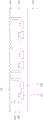
图15绘示图14的发光二极管晶片100的放大图。在图15中,发光二极管晶片100包含图案化半导体层110’、绝缘层120、第一电极131与第二电极132。图案化半导体层110’具有侧壁111a、相对的顶侧111b与底侧111c。侧壁111a连接顶侧111b与底侧111c,且顶侧111b上具有凹凸结构113。凹凸结构113的凹凸图形可为规则的或不规则的。在一些实施方式中,图案化半导体层110’为多层结构,并包含由上而下的第一半导体层114、主动层116与第二半导体层118。第一半导体层114具有第一型半导体材料,例如n型,第二半导体层118则具有与第一型半导体材料不同型的第二半导体材料,例如p型。主动层116可为加入量子井结构与/或量子点结构的层,因此当电流通过主动层116时,主动层116可发出特定的光。FIG. 15 is an enlarged view of the
绝缘层120覆盖图案化半导体层110’的侧壁111a与底侧111c。在一些实施方式中,绝缘层120可以被图案化半导体层110’的主动层116发出的光穿透,以获得具有大出光角度的光形。在一些实施方式中,绝缘层120可反射从图案化半导体层110’的主动层116发出的光,以获得集中于正向出光的光形。在一些实施方式中,绝缘层120包含分布式布拉格反射器。绝缘层120具有突出部124,突出部124沿平行侧壁111a的方向延伸突出于凹凸结构113。具有绝缘层120的突出部124的发光二极管晶片100容易通过突出部124固定在图11中的胶材154。再者,绝缘层120的突出部124的存在降低胶材154与发光二极管晶片100之间的附着力,因此在转移发光二极管晶片100至第三载板162(参考图13)时,不会因过大的附着力使得发光二极管晶片100被胶材154损坏、沾粘或是无法脱离胶材154,以增加转移发光二极管晶片100的良率。在一些实施方式中,绝缘层120的厚度T1在约0.4微米至约3.5微米的范围内。若绝缘层120的厚度T1落于所揭露的范围外,则绝缘层120的突出部124不易刺入胶材154,使得发光二极管晶片100不易固定在胶材154上。The insulating
在一些实施方式中,凹凸结构113的最高点与突出部124的最高点之间具有垂直距离D1,且垂直距离D1在大于0.5微米且小于4倍的图案化半导体层110’厚度T2之间。在另一些实施方式中,突出部124的最高点与凹凸结构113的中心点C形成连线L1,连线L1与图案化半导体层110’的水平截面HL形成第一角度α1,第一角度α1在1度至10度的范围之间。当绝缘层120可反射主动层116发出的光时,可借此将发光二极管晶片100的出光角限制在预设的范围内,例如约小于120度。在一些实施方式中,图案化半导体层110’的水平截面可以是第一半导体层114与主动层116的交界面或第二半导体层118与主动层116的交界面。In some embodiments, there is a vertical distance D1 between the highest point of the concave-
在一些实施方式中,突出部124的上表面向图案化半导体层110’倾斜。可根据不同情况决定突出部124的上表面的倾斜程度,例如当胶体154粘度较大时,较大的倾斜程度可以使突出部124更容易穿进胶体154中。在一些实施方式中,突出部124的上表面的延伸线L2与图案化半导体层110’的水平截面形成第二角度α2,凹凸结构113的任一表面的延伸线L3与图案化半导体层110’的水平截面形成第三角度α3,且第二角度α2小于第三角度α3。当第二角度α2小于第三角度α3,且绝缘层120的突出部124可反射从凹凸结构113射出的光时,可使发光二极管晶片100的光集中向上射出。In some embodiments, the upper surface of the
第一电极131与第二电极132位于图案化半导体层110’的底侧111c,且第二电极132与第一电极131相邻。第一电极131贯穿绝缘层120并与第一半导体层114接触,而第二电极132贯穿绝缘层120并与第二半导体层118接触。第一电极131与第二电极132可进一步分别与第三载板162上的接触垫164、166电性连接。The
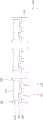
绝缘层120的突出部124亦可具有不同的形状。举例而言,突出部124的上表面可为平面,如图16所示,其绘示根据本揭露的一些实施方式的发光二极管晶片100的剖面图。在图16中,突出部124的上表面可实质平行于水平截面HL。至于图16的发光二极管晶片100的其他细节皆与图15的发光二极管晶片100相同或相似,因此便不再赘述。The protruding
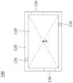
图17A至图18B绘示根据本揭露的一些实施方式的发光二极管晶片100的上视图。在一些实施方式中,绝缘层120的突出部124也可具有不同的俯视图案。举例而言,在图17A中,绝缘层120的突出部124为封闭环状,且沿图案化半导体层110’的周缘设置以环绕图案化半导体层110’。在图17B中,绝缘层120的突出部124为包含至少一个开口123的非封闭环状,且沿图案化半导体层110’周缘设置以环绕图案化半导体层110’。应注意开口123的位置不局限于如图17B所示的位置上。举例而言,开口123可位于突出部124的较长边处,如图17B所示。开口123也可位于突出部124的较短边处。开口123暴露底下的绝缘层120,意即在开口123中,绝缘层120的开口123底部与图案化半导体层110’的顶侧111b的高度相同。在一些实施方式中,绝缘层120的突出部124也可包含至少一对子突出部126,如图18A与图18B所示。子突出部126可具有任何适合的形状,例如矩形(图18A)、圆形(图18B)或其他合适的形状等。每对子突出部126以图案化半导体层110’的几何中心P点对称地设置于图案化半导体层110’周缘上。子突出部126的大小足够穿入胶材154并提供与胶材154之间的附着力,而不使得过多部分的发光二极管晶片100与胶材154接触。17A to 18B illustrate top views of an
图19绘示根据本揭露的一些实施方式的发光二极管晶片100的剖面图。在一些实施方式中,凹凸结构113也可包含聚合物104。举例而言,当发光二极管晶片100是由图1B所示的结构发展而成,由于聚合物层104不会在制程中完全被移除,在发光二极管晶片100的最终结构中,聚合物层104仍会在图案化半导体层110’上。因此,凹凸结构113也可包含聚合物104,如图19所示。FIG. 19 illustrates a cross-sectional view of an
综上所述,本揭露中的绝缘层的突出部可以减少发光二极管晶片与胶材的接触面积,进而降低两者之间的粘着力。因此,在转移发光二极管晶片时,发光二极管晶片不会因为发光二极管晶片与胶材之间过大的粘着力而无法顺利分离,使得转移发光二极管晶片的成功率可提升。To sum up, the protruding portion of the insulating layer in the present disclosure can reduce the contact area between the LED chip and the adhesive, thereby reducing the adhesion between the two. Therefore, when transferring the LED chip, the LED chip will not be unable to be separated smoothly due to excessive adhesion between the LED chip and the adhesive material, so that the success rate of transferring the LED chip can be improved.
虽然本发明已以实施方式揭露如上,然其并非用以限定本发明,任何熟悉此技艺者,在不脱离本发明的精神和范围内,当可作各种的更动与润饰,因此本发明的保护范围当视所附的权利要求书所界定的范围为准。Although the present invention has been disclosed above in terms of implementation, it is not intended to limit the present invention. Any skilled person can make various changes and modifications without departing from the spirit and scope of the present invention. Therefore, the present invention The scope of protection should be based on the scope defined by the appended claims.
Claims (13)
Translated fromChineseApplications Claiming Priority (2)
| Application Number | Priority Date | Filing Date | Title |
|---|---|---|---|
| TW110130520 | 2021-08-18 | ||
| TW110130520ATWI777733B (en) | 2021-08-18 | 2021-08-18 | Light emitting diode chip and light emitting diode device |
Publications (1)
| Publication Number | Publication Date |
|---|---|
| CN115708229Atrue CN115708229A (en) | 2023-02-21 |
Family
ID=84958078
Family Applications (1)
| Application Number | Title | Priority Date | Filing Date |
|---|---|---|---|
| CN202210954438.8APendingCN115708229A (en) | 2021-08-18 | 2022-08-10 | Light emitting diode wafer and light emitting diode wafer device |
Country Status (3)
| Country | Link |
|---|---|
| US (1) | US20230057589A1 (en) |
| CN (1) | CN115708229A (en) |
| TW (1) | TWI777733B (en) |
Family Cites Families (10)
| Publication number | Priority date | Publication date | Assignee | Title |
|---|---|---|---|---|
| TW201234574A (en)* | 2011-02-01 | 2012-08-16 | Pinecone En Inc | Light-emitting-diode array and manufacturing method thereof |
| JP4989773B1 (en)* | 2011-05-16 | 2012-08-01 | 株式会社東芝 | Semiconductor light emitting device |
| JP5377725B1 (en)* | 2012-08-21 | 2013-12-25 | 株式会社東芝 | Semiconductor light emitting device |
| DE102015112538B4 (en)* | 2015-07-30 | 2023-08-03 | OSRAM Opto Semiconductors Gesellschaft mit beschränkter Haftung | Optoelectronic component and a method for producing an optoelectronic component |
| KR101754528B1 (en)* | 2016-03-23 | 2017-07-06 | 한국광기술원 | Transfer assembly with dry adhesion structure and method for transferring led structure assembly using the same and led structure assembly |
| CN109860364B (en)* | 2017-08-30 | 2020-09-01 | 天津三安光电有限公司 | Light emitting diode |
| CN109786307B (en)* | 2017-11-15 | 2021-02-05 | 鸿富锦精密工业(深圳)有限公司 | Preparation method of micro LED display panel |
| CN108231968B (en)* | 2017-12-11 | 2020-02-11 | 厦门市三安光电科技有限公司 | Micro light emitting diode and transfer method thereof |
| CN112397491B (en)* | 2020-11-16 | 2024-12-27 | 錼创显示科技股份有限公司 | Micro light emitting diode display element and method for manufacturing the same |
| US12376428B2 (en)* | 2021-05-10 | 2025-07-29 | Xiamen San'an Optoelectronics Co., Ltd. | Micro light-emitting diode and micro light-emitting device with rough surface and protection layer |
- 2021
- 2021-08-18TWTW110130520Apatent/TWI777733B/enactive
- 2022
- 2022-05-10USUS17/662,658patent/US20230057589A1/enactivePending
- 2022-08-10CNCN202210954438.8Apatent/CN115708229A/enactivePending
Also Published As
| Publication number | Publication date |
|---|---|
| US20230057589A1 (en) | 2023-02-23 |
| TWI777733B (en) | 2022-09-11 |
| TW202310445A (en) | 2023-03-01 |
Similar Documents
| Publication | Publication Date | Title |
|---|---|---|
| US9178107B2 (en) | Wafer-level light emitting diode structure, light emitting diode chip, and method for forming the same | |
| CN101515621B (en) | Light emitting diode chip, manufacturing method and packaging method | |
| CN102593275B (en) | Method for manufacturing light-emitting diode packaging structure and light-emitting diode element | |
| CN104170100B (en) | Light emitting diode and its manufacture method | |
| CN102637784B (en) | Light-emitting diode packaging substrate and manufacturing method thereof | |
| EP2232594B1 (en) | Semiconductor light emitting device and method of fabricating the same | |
| CN101145570A (en) | Light emitting diode structure | |
| WO2021087686A1 (en) | Light-emitting diode and manufacturing method therefor | |
| CN102194945A (en) | Light emitting device and method of forming the same | |
| EP2528114A2 (en) | Light emitting device, light emitting device package, and light unit | |
| CN103928585B (en) | Luminescent device | |
| CN110676355B (en) | Method of making a light-emitting element | |
| US20250287738A1 (en) | Semiconductor chip and light-emitting device | |
| JP4449919B2 (en) | Method for manufacturing light emitting device | |
| CN114530534A (en) | LED chip and preparation method thereof | |
| CN105518879A (en) | Light emitting element | |
| CN116666515A (en) | Micro light-emitting diode display chip and manufacturing method | |
| CN210897328U (en) | LED chip and light-emitting module | |
| US8421098B2 (en) | Semiconductor light emitting device having a roughness on a channel layer | |
| CN110429098B (en) | A display panel, its manufacturing method, and display device | |
| TWI661584B (en) | Light emitting chip, packaged structure and associated manufacturing method | |
| TW201032349A (en) | Light-emitting diode chip, and manufacturing method and packaging method therefor | |
| CN115708229A (en) | Light emitting diode wafer and light emitting diode wafer device | |
| CN116779737A (en) | LED chip and preparation method thereof | |
| CN114883469B (en) | Light emitting diode chip for improving current conduction and preparation method thereof |
Legal Events
| Date | Code | Title | Description |
|---|---|---|---|
| PB01 | Publication | ||
| PB01 | Publication | ||
| SE01 | Entry into force of request for substantive examination | ||
| SE01 | Entry into force of request for substantive examination |