CN115699342A - Optical device and method of manufacturing optical device - Google Patents
Optical device and method of manufacturing optical deviceDownload PDFInfo
- Publication number
- CN115699342A CN115699342ACN202180037843.7ACN202180037843ACN115699342ACN 115699342 ACN115699342 ACN 115699342ACN 202180037843 ACN202180037843 ACN 202180037843ACN 115699342 ACN115699342 ACN 115699342A
- Authority
- CN
- China
- Prior art keywords
- optical device
- light emitting
- layer
- emitting structure
- spacer layer
- Prior art date
- Legal status (The legal status is an assumption and is not a legal conclusion. Google has not performed a legal analysis and makes no representation as to the accuracy of the status listed.)
- Pending
Links
Images


Classifications
- H—ELECTRICITY
- H10—SEMICONDUCTOR DEVICES; ELECTRIC SOLID-STATE DEVICES NOT OTHERWISE PROVIDED FOR
- H10H—INORGANIC LIGHT-EMITTING SEMICONDUCTOR DEVICES HAVING POTENTIAL BARRIERS
- H10H20/00—Individual inorganic light-emitting semiconductor devices having potential barriers, e.g. light-emitting diodes [LED]
- H10H20/80—Constructional details
- H10H20/84—Coatings, e.g. passivation layers or antireflective coatings
- H10H20/841—Reflective coatings, e.g. dielectric Bragg reflectors
- H—ELECTRICITY
- H10—SEMICONDUCTOR DEVICES; ELECTRIC SOLID-STATE DEVICES NOT OTHERWISE PROVIDED FOR
- H10H—INORGANIC LIGHT-EMITTING SEMICONDUCTOR DEVICES HAVING POTENTIAL BARRIERS
- H10H20/00—Individual inorganic light-emitting semiconductor devices having potential barriers, e.g. light-emitting diodes [LED]
- H10H20/01—Manufacture or treatment
- H10H20/011—Manufacture or treatment of bodies, e.g. forming semiconductor layers
- H10H20/017—Etching
- H—ELECTRICITY
- H10—SEMICONDUCTOR DEVICES; ELECTRIC SOLID-STATE DEVICES NOT OTHERWISE PROVIDED FOR
- H10H—INORGANIC LIGHT-EMITTING SEMICONDUCTOR DEVICES HAVING POTENTIAL BARRIERS
- H10H20/00—Individual inorganic light-emitting semiconductor devices having potential barriers, e.g. light-emitting diodes [LED]
- H10H20/01—Manufacture or treatment
- H10H20/034—Manufacture or treatment of coatings
- H—ELECTRICITY
- H10—SEMICONDUCTOR DEVICES; ELECTRIC SOLID-STATE DEVICES NOT OTHERWISE PROVIDED FOR
- H10H—INORGANIC LIGHT-EMITTING SEMICONDUCTOR DEVICES HAVING POTENTIAL BARRIERS
- H10H20/00—Individual inorganic light-emitting semiconductor devices having potential barriers, e.g. light-emitting diodes [LED]
- H10H20/80—Constructional details
- H10H20/81—Bodies
- H10H20/811—Bodies having quantum effect structures or superlattices, e.g. tunnel junctions
- H10H20/812—Bodies having quantum effect structures or superlattices, e.g. tunnel junctions within the light-emitting regions, e.g. having quantum confinement structures
- H—ELECTRICITY
- H10—SEMICONDUCTOR DEVICES; ELECTRIC SOLID-STATE DEVICES NOT OTHERWISE PROVIDED FOR
- H10H—INORGANIC LIGHT-EMITTING SEMICONDUCTOR DEVICES HAVING POTENTIAL BARRIERS
- H10H20/00—Individual inorganic light-emitting semiconductor devices having potential barriers, e.g. light-emitting diodes [LED]
- H10H20/80—Constructional details
- H10H20/81—Bodies
- H10H20/819—Bodies characterised by their shape, e.g. curved or truncated substrates
- H10H20/82—Roughened surfaces, e.g. at the interface between epitaxial layers
- H—ELECTRICITY
- H10—SEMICONDUCTOR DEVICES; ELECTRIC SOLID-STATE DEVICES NOT OTHERWISE PROVIDED FOR
- H10H—INORGANIC LIGHT-EMITTING SEMICONDUCTOR DEVICES HAVING POTENTIAL BARRIERS
- H10H20/00—Individual inorganic light-emitting semiconductor devices having potential barriers, e.g. light-emitting diodes [LED]
- H10H20/80—Constructional details
- H10H20/81—Bodies
- H10H20/822—Materials of the light-emitting regions
- H10H20/824—Materials of the light-emitting regions comprising only Group III-V materials, e.g. GaP
- H10H20/825—Materials of the light-emitting regions comprising only Group III-V materials, e.g. GaP containing nitrogen, e.g. GaN
- H—ELECTRICITY
- H10—SEMICONDUCTOR DEVICES; ELECTRIC SOLID-STATE DEVICES NOT OTHERWISE PROVIDED FOR
- H10H—INORGANIC LIGHT-EMITTING SEMICONDUCTOR DEVICES HAVING POTENTIAL BARRIERS
- H10H20/00—Individual inorganic light-emitting semiconductor devices having potential barriers, e.g. light-emitting diodes [LED]
- H10H20/80—Constructional details
- H10H20/83—Electrodes
- H10H20/831—Electrodes characterised by their shape
- H—ELECTRICITY
- H10—SEMICONDUCTOR DEVICES; ELECTRIC SOLID-STATE DEVICES NOT OTHERWISE PROVIDED FOR
- H10H—INORGANIC LIGHT-EMITTING SEMICONDUCTOR DEVICES HAVING POTENTIAL BARRIERS
- H10H20/00—Individual inorganic light-emitting semiconductor devices having potential barriers, e.g. light-emitting diodes [LED]
- H10H20/80—Constructional details
- H10H20/83—Electrodes
- H10H20/832—Electrodes characterised by their material
- H10H20/835—Reflective materials
- H—ELECTRICITY
- H10—SEMICONDUCTOR DEVICES; ELECTRIC SOLID-STATE DEVICES NOT OTHERWISE PROVIDED FOR
- H10H—INORGANIC LIGHT-EMITTING SEMICONDUCTOR DEVICES HAVING POTENTIAL BARRIERS
- H10H20/00—Individual inorganic light-emitting semiconductor devices having potential barriers, e.g. light-emitting diodes [LED]
- H10H20/80—Constructional details
- H10H20/84—Coatings, e.g. passivation layers or antireflective coatings
- H—ELECTRICITY
- H10—SEMICONDUCTOR DEVICES; ELECTRIC SOLID-STATE DEVICES NOT OTHERWISE PROVIDED FOR
- H10H—INORGANIC LIGHT-EMITTING SEMICONDUCTOR DEVICES HAVING POTENTIAL BARRIERS
- H10H20/00—Individual inorganic light-emitting semiconductor devices having potential barriers, e.g. light-emitting diodes [LED]
- H10H20/80—Constructional details
- H10H20/85—Packages
- H10H20/855—Optical field-shaping means, e.g. lenses
- H10H20/856—Reflecting means
- H—ELECTRICITY
- H10—SEMICONDUCTOR DEVICES; ELECTRIC SOLID-STATE DEVICES NOT OTHERWISE PROVIDED FOR
- H10H—INORGANIC LIGHT-EMITTING SEMICONDUCTOR DEVICES HAVING POTENTIAL BARRIERS
- H10H29/00—Integrated devices, or assemblies of multiple devices, comprising at least one light-emitting semiconductor element covered by group H10H20/00
- H10H29/10—Integrated devices comprising at least one light-emitting semiconductor component covered by group H10H20/00
- H10H29/14—Integrated devices comprising at least one light-emitting semiconductor component covered by group H10H20/00 comprising multiple light-emitting semiconductor components
- H10H29/142—Two-dimensional arrangements, e.g. asymmetric LED layout
- H—ELECTRICITY
- H01—ELECTRIC ELEMENTS
- H01L—SEMICONDUCTOR DEVICES NOT COVERED BY CLASS H10
- H01L25/00—Assemblies consisting of a plurality of semiconductor or other solid state devices
- H01L25/03—Assemblies consisting of a plurality of semiconductor or other solid state devices all the devices being of a type provided for in a single subclass of subclasses H10B, H10D, H10F, H10H, H10K or H10N, e.g. assemblies of rectifier diodes
- H01L25/04—Assemblies consisting of a plurality of semiconductor or other solid state devices all the devices being of a type provided for in a single subclass of subclasses H10B, H10D, H10F, H10H, H10K or H10N, e.g. assemblies of rectifier diodes the devices not having separate containers
- H01L25/075—Assemblies consisting of a plurality of semiconductor or other solid state devices all the devices being of a type provided for in a single subclass of subclasses H10B, H10D, H10F, H10H, H10K or H10N, e.g. assemblies of rectifier diodes the devices not having separate containers the devices being of a type provided for in group H10H20/00
- H01L25/0753—Assemblies consisting of a plurality of semiconductor or other solid state devices all the devices being of a type provided for in a single subclass of subclasses H10B, H10D, H10F, H10H, H10K or H10N, e.g. assemblies of rectifier diodes the devices not having separate containers the devices being of a type provided for in group H10H20/00 the devices being arranged next to each other
- H—ELECTRICITY
- H10—SEMICONDUCTOR DEVICES; ELECTRIC SOLID-STATE DEVICES NOT OTHERWISE PROVIDED FOR
- H10H—INORGANIC LIGHT-EMITTING SEMICONDUCTOR DEVICES HAVING POTENTIAL BARRIERS
- H10H20/00—Individual inorganic light-emitting semiconductor devices having potential barriers, e.g. light-emitting diodes [LED]
- H10H20/01—Manufacture or treatment
- H10H20/011—Manufacture or treatment of bodies, e.g. forming semiconductor layers
- H10H20/013—Manufacture or treatment of bodies, e.g. forming semiconductor layers having light-emitting regions comprising only Group III-V materials
- H10H20/0137—Manufacture or treatment of bodies, e.g. forming semiconductor layers having light-emitting regions comprising only Group III-V materials the light-emitting regions comprising nitride materials
- H—ELECTRICITY
- H10—SEMICONDUCTOR DEVICES; ELECTRIC SOLID-STATE DEVICES NOT OTHERWISE PROVIDED FOR
- H10H—INORGANIC LIGHT-EMITTING SEMICONDUCTOR DEVICES HAVING POTENTIAL BARRIERS
- H10H20/00—Individual inorganic light-emitting semiconductor devices having potential barriers, e.g. light-emitting diodes [LED]
- H10H20/01—Manufacture or treatment
- H10H20/036—Manufacture or treatment of packages
- H10H20/0363—Manufacture or treatment of packages of optical field-shaping means
Landscapes
- Led Devices (AREA)
Abstract
Description
Translated fromChinese技术领域technical field
本发明涉及发光器件阵列以及形成发光器件阵列的方法。具体地,但非排他地,本发明涉及具有优化的光提取的发光器件阵列。The present invention relates to arrays of light emitting devices and methods of forming arrays of light emitting devices. In particular, but not exclusively, the invention relates to arrays of light emitting devices with optimized light extraction.
背景技术Background technique
众所周知,发光二极管(LED)器件为各种各样的应用提供了高效的光源。LED光产生效率和提取量的提高、以及更小LED(具有更小的发光表面积)的生产和不同波长的LED发射器在阵列中的集成,导致了提供具有多种应用的高质量彩色阵列,尤其是在显示技术中。Light emitting diode (LED) devices are well known to provide highly efficient light sources for a wide variety of applications. Improvements in LED light generation efficiency and extraction, as well as the production of smaller LEDs (with smaller light-emitting surface areas) and the integration of LED emitters of different wavelengths in arrays have led to the provision of high-quality color arrays with a variety of applications, Especially in display technology.
几种显示技术正被考虑并用于微型LED显示器,以用于各种应用,包括增强现实、合并现实、虚拟现实以及直视显示,比如智能手表和移动设备。比如数字微镜(DMD)和硅基液晶(LCoS)等技术是基于反射技术的,其中,使用外部光源以时间顺序模式产生红色光子、绿色光子和蓝色光子,并且像素要么将光从光学元件(DMD)转移开要么吸收光(LCoS)来调整像素的亮度以便形成图像。液晶显示器(LCD)通常使用背光、可寻址背板上的LCD面板和滤色器来产生图像。需要背板来打开和关闭单个像素,并为每个视频帧调整单个像素的亮度。比如有机发光二极管(OLED)或有源矩阵OLED(AMOLED)、以及最近的微型LED等发光显示技术越来越多,因为它们为不受限制的微型显示应用提供更低的功耗和更高的图像对比度。特别是微型LED,与微型OLED和AMOLED显示器相比提供更高的效率和更好的可靠性。Several display technologies are being considered and used in micro-LED displays for various applications including augmented reality, merged reality, virtual reality, and direct-view displays, such as smart watches and mobile devices. Technologies such as digital micromirror (DMD) and liquid crystal on silicon (LCoS) are based on reflection technology, where an external light source is used to generate red photons, green photons, and blue photons in a time-sequential pattern, and the pixels either transfer the light from the optical element (DMD) shifts or absorbs light (LCoS) to adjust the brightness of pixels to form an image. Liquid crystal displays (LCDs) typically use a backlight, an LCD panel on an addressable backplane, and color filters to produce images. Backplanes are needed to turn individual pixels on and off, and to adjust the brightness of individual pixels for each video frame. Light-emitting display technologies such as organic light-emitting diodes (OLEDs) or active-matrix OLEDs (AMOLEDs), and more recently micro-LEDs, are increasingly available because they offer lower power consumption and higher Image contrast. Micro LEDs, in particular, offer higher efficiency and better reliability than micro OLED and AMOLED displays.
本文档中描述的本发明涉及一种用于制造高效微型LED阵列的方法,该阵列结合了提高内部量子效率(IQE)和光提取效率(LEE)的技术,以提高效率和亮度品质因数。The invention described in this document relates to a method for fabricating high-efficiency micro-LED arrays incorporating techniques to increase internal quantum efficiency (IQE) and light extraction efficiency (LEE) to improve efficiency and luminance figure of merit.
旨在提高光提取效率的结构在LED行业中是众所周知的,包括使用伪抛物线形MESA将多量子阱(MQW)中产生的光子引导至发射表面。Structures aimed at improving light extraction efficiency are well known in the LED industry, including the use of pseudoparabolic MESAs to guide photons generated in multiple quantum wells (MQWs) to the emitting surface.
用于制造具有这种形状的MESA的技术涉及比如反应离子刻蚀(RIE)或电感耦合刻蚀(ICP)等技术。在这种刻蚀技术中,使用包括RF、高压(DC偏压)和反应气体(通常包括自由基)的高能等离子体来选择性地刻蚀半导体材料。使用光刻工艺定义特征,该光刻工艺使用光敏材料来定义将经受刻蚀工艺的区域和将保持未刻蚀的区域。MESA的精确形状可以通过用于定义图案的光敏材料的轮廓以及通过刻蚀压力、功率、气流和气体种类来控制。Techniques for fabricating MESAs with such shapes involve techniques such as reactive ion etching (RIE) or inductively coupled etching (ICP). In this etching technique, semiconductor materials are selectively etched using high energy plasmas including RF, high voltage (DC bias), and reactive gases (often including free radicals). The features are defined using a photolithographic process that uses photosensitive materials to define the areas that will be subjected to the etch process and the areas that will remain unetched. The precise shape of the MESA can be controlled by the profile of the photosensitive material used to define the pattern as well as by etch pressure, power, gas flow and gas species.
这不仅使制造工艺复杂化,而且由于这种刻蚀工艺,MESA的边缘可能会被损坏,这会影响微型LED的IQE。This not only complicates the fabrication process, but also the edge of the MESA may be damaged due to this etching process, which affects the IQE of the micro-LED.
如图1所示,随着DC偏压和等离子体密度的增大,对特征的边缘造成更多损坏,导致了由晶体损坏、氮空位和悬空键形成的表面泄漏路径。由于表面的高能离子轰击,干法刻蚀会产生许多晶体缺陷。悬空键很容易被氧化,并且晶体损坏会在能带中产生许多缺陷能级,这些缺陷能级充当表面的载流子复合中心,从而导致非辐射复合。As shown in Figure 1, as the DC bias and plasma density increase, more damage is done to the edges of the features, resulting in surface leakage paths formed by crystal damage, nitrogen vacancies, and dangling bonds. Dry etching produces many crystal defects due to the high-energy ion bombardment of the surface. Dangling bonds are easily oxidized, and crystal damage creates many defect levels in the energy bands, which act as carrier recombination centers at the surface, leading to nonradiative recombination.
表面复合速度(非辐射复合速度)比块体MQW中的辐射复合速度快,因此小的微型LED易受到表面复合的影响,其结果是IQE降低。The surface recombination velocity (non-radiative recombination velocity) is faster than the radiative recombination velocity in bulk MQWs, so small micro-LEDs are susceptible to surface recombination with a consequent reduction in IQE.
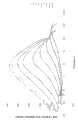
在MESA刻蚀期间造成的损坏的广为流传的结果是随着微型LED尺寸的缩小会降低效率,如图2所示。外部量子效率(EQE)是IQE(所产生的光子数与电子数的比率)的产物。驱动这种趋势的机制是微型LED的周长与面积的比率。随着微型LED尺寸的减小,侧壁的面积相对于MQW的面积增大,因此微型LED的边缘的表面泄漏路径导致非辐射复合增加。A well-publicized consequence of damage caused during MESA etch is reduced efficiency as micro-LEDs shrink in size, as shown in Figure 2. External Quantum Efficiency (EQE) is a product of IQE (the ratio of the number of photons produced to the number of electrons). The mechanism driving this trend is the perimeter-to-area ratio of microLEDs. As the size of the micro-LED decreases, the area of the sidewalls increases relative to the area of the MQW, thus surface leakage paths at the edge of the micro-LED lead to increased non-radiative recombination.
用于增强现实的微型LED显示器和头戴式显示器将在1A/cm2至10A/cm2的电流密度下操作。这可能意味着与大LED相比,小LED的效率降低为其1/20。Micro-LED displays and head-mounted displays for augmented reality will operate at current densities of 1A/cm2 to 10A/cm2. This can mean that the efficiency of a small LED is reduced by 1/20 compared to a large LED.
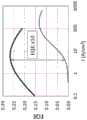
如图3所示,通过修复由MESA刻蚀造成的损坏,可以显著地提高微型LED的效率。通过执行优化的损坏修复方案,通常可以使EQE提高10倍。在损坏修复之后峰值EQE增大,并且峰值EQE出现在较低的电流密度下,使得在典型操作条件下,可以获得10倍的效率提升。然而,这种方案与保留MESA形状(该形状是针对高LEE优化的)不兼容,因为修复工艺会去除被MESA刻蚀损坏的半导体材料,如图4所示。As shown in Figure 3, the efficiency of micro-LEDs can be significantly improved by repairing the damage caused by MESA etching. A 10x improvement in EQE is typically achieved by implementing an optimized damage repair scheme. The peak EQE increases after damage repair and occurs at lower current densities, enabling a 10-fold efficiency improvement under typical operating conditions. However, this scheme is not compatible with preserving the MESA shape (which is optimized for high LEE), because the repair process removes the semiconductor material damaged by the MESA etch, as shown in Figure 4.
发明内容Contents of the invention
为了缓解至少一些上述问题,根据所附权利要求提供了一种光学器件。进一步地,根据所附权利要求提供了一种光学器件阵列和一种形成一个或多个光学器件的方法。To alleviate at least some of the above problems, an optical device is provided according to the appended claims. Further, there is provided an array of optical devices and a method of forming one or more optical devices according to the appended claims.
在本发明的第一方面中,提供了一种光学器件,该光学器件包括:发光结构,该发光结构具有基本上竖直的侧壁,该发光结构包括有源层,该有源层被配置为在电流被施加至该器件时发光;电绝缘的、光学透明的隔垫物层,该隔垫物层具有面向该发光结构的侧壁的内部面和相反的外部面,其中,该隔垫物层被配置为增强从该有源层的光提取;以及反射性的导电反射镜层,该反射镜层设置在该隔垫物层的外部面上。In a first aspect of the present invention, an optical device is provided, comprising: a light emitting structure having substantially vertical sidewalls, the light emitting structure comprising an active layer configured To emit light when electric current is applied to the device; an electrically insulating, optically transparent spacer layer having an inner face facing the sidewall of the light emitting structure and an opposite outer face, wherein the spacer an object layer configured to enhance light extraction from the active layer; and a reflective conductive mirror layer disposed on an outer face of the spacer object layer.
有利地,该隔垫物材料用作光学部件以增强从该发光结构的有源层的光提取,而金属材料用作隔垫物侧面的反射镜层,以进一步增强光提取。Advantageously, the spacer material is used as an optical component to enhance light extraction from the active layer of the light emitting structure, while the metal material is used as a mirror layer on the side of the spacer to further enhance light extraction.
优选地,该光学器件进一步包括在该发光结构与该隔垫物层之间的钝化层。Preferably, the optical device further comprises a passivation layer between the light emitting structure and the spacer layer.
优选地,该钝化层是二氧化硅、氧化铝或立方氮化铝中的一种。Preferably, the passivation layer is one of silicon dioxide, aluminum oxide or cubic aluminum nitride.
该钝化层的作用是降低表面状态,否则会使该器件的电性能劣化。The function of the passivation layer is to reduce the surface states that would otherwise degrade the electrical properties of the device.
优选地,该发光结构具有第一发光表面,其中,该光学器件进一步包括该发光表面上的光提取特征。该光提取特征为该器件的光学性能提供了进一步增强。Preferably, the light emitting structure has a first light emitting surface, wherein the optical device further comprises light extraction features on the light emitting surface. This light extraction feature provides a further enhancement to the optical performance of the device.
优选地,该光提取特征采取凸透镜的形式。Preferably, the light extraction feature takes the form of a convex lens.
优选地,该凸透镜的曲率半径为3微米。已经发现这提供了最大的光提取。Preferably, the curvature radius of the convex lens is 3 microns. It has been found that this provides maximum light extraction.
优选地,该隔垫物层的外部面具有伪抛物线轮廓或抛物线轮廓。抛物线形状的作用是将发射的光子引向该器件的该发光表面,使得这些光子以低于临界角的入射角入射在所述表面上,从而允许以高频率将光子提取到空气中。Preferably, the outer face of the spacer layer has a pseudo-parabolic or parabolic profile. The effect of the parabolic shape is to direct the emitted photons towards the light emitting surface of the device such that these photons are incident on the surface at angles of incidence below the critical angle, allowing photons to be extracted into air at high frequencies.
优选地,该隔垫物层的外部面的轮廓近似于具有两个控制点且贝塞尔系数为0.5的贝塞尔曲线。已经发现这提供了最大的光提取。Preferably, the profile of the outer face of the spacer layer approximates a Bezier curve with two control points and a Bezier coefficient of 0.5. It has been found that this provides maximum light extraction.
优选地,该隔垫物是二氧化硅、氮化硅或氧化钛中的一种。Preferably, the spacer is one of silicon dioxide, silicon nitride or titanium oxide.
优选地,该发光结构进一步包括n包层,并且其中,该反射镜层与该n包层电接触,使得该反射镜层形成该光学器件的第一电极。有利地,该反射镜层进一步用作该光学器件的电流扩散层。Preferably, the light emitting structure further comprises an n-cladding layer, and wherein the mirror layer is in electrical contact with the n-cladding layer, such that the mirror layer forms a first electrode of the optical device. Advantageously, the mirror layer further serves as a current spreading layer of the optical device.
优选地,该发光结构进一步包括与该光学器件的第二电极电接触的p包层。Preferably, the light emitting structure further comprises a p-cladding layer in electrical contact with the second electrode of the optical device.
优选地,该第二电极形成在该发光结构的与该第一表面相反的第二表面上,并且其中,该第二电极由反射材料制成。与该发光表面相反的反射表面的布置改善了光提取,从而提高了该光学器件的效率。Preferably, the second electrode is formed on a second surface of the light emitting structure opposite to the first surface, and wherein the second electrode is made of a reflective material. The arrangement of the reflective surface opposite the light-emitting surface improves light extraction, thereby increasing the efficiency of the optic.
优选地,该有源层包括一个或多个量子阱。Preferably, the active layer comprises one or more quantum wells.
优选地,该发光结构进一步包括缓冲层和超晶格。Preferably, the light emitting structure further includes a buffer layer and a superlattice.
优选地,该发光结构包括氮化铟镓。Preferably, the light emitting structure includes InGaN.
优选地,该发光结构具有正方形、圆形、三角形或五边形的截面中的一种。Preferably, the light emitting structure has one of square, circular, triangular or pentagonal cross sections.
优选地,该发光结构具有粗糙化的侧壁。已经发现这改善了亮度均匀性并且进一步增强了光提取。Preferably, the light emitting structure has roughened sidewalls. It has been found that this improves brightness uniformity and further enhances light extraction.
优选地,该隔垫物层的内部面由第一材料形成,而该隔垫物层的外部面由第二材料形成。这允许使用具有不同折射率的材料,使得所发射的光子可以被更好地引向发光表面。Preferably, the inner face of the spacer layer is formed from a first material and the outer face of the spacer layer is formed from a second material. This allows the use of materials with different refractive indices so that emitted photons can be better directed towards the light-emitting surface.
优选地,该第一材料具有比该第二材料高的折射率,使得光越来越多地被反射回该发光结构的发光表面。Preferably, the first material has a higher refractive index than the second material such that light is increasingly reflected back to the light emitting surface of the light emitting structure.
在本发明的第二方面中,提供了一种由上述光学器件组成的阵列。In a second aspect of the present invention, an array consisting of the above optical devices is provided.
在本发明的第三方面中,提供了一种制造上述光学器件的方法。In a third aspect of the present invention, there is provided a method of manufacturing the above-mentioned optical device.
本发明的更多方面将从说明书和所附权利要求中变得明显。Further aspects of the invention will be apparent from the description and appended claims.
附图说明Description of drawings
仅通过举例的方式参考附图来描述本发明实施例的详细说明,在附图中:The detailed description of embodiments of the present invention is described by way of example only with reference to the accompanying drawings, in which:
图1示出了随着等离子体功率和DC偏压的增大对InGaN材料的晶体损坏;Figure 1 shows crystal damage to InGaN materials with increasing plasma power and DC bias;
图2示出了针对微型LED尺寸从A1(256μm)减小至A9(1μm),外部量子效率(EQE)与电流密度的关系;Figure 2 shows the external quantum efficiency (EQE) versus current density for micro-LED size reduction from A1 (256 μm) to A9 (1 μm);
图3示出了在有和没有MESA损坏减少和修复的情况下微型LED的EQE;Figure 3 shows the EQE of micro-LEDs with and without MESA damage reduction and repair;
图4示出了在损坏修复工艺之前(a)和之后(b),经刻蚀的MESA的截面;Figure 4 shows a cross-section of the etched MESA before (a) and after (b) the damage repair process;
图5示出了根据本发明的一方面的光学器件;Figure 5 shows an optical device according to an aspect of the present invention;
图6示出了根据曲率半径R和贝塞尔系数B的不同而具有不同形状的凸透镜和隔垫物的一系列光学器件;Fig. 6 shows a series of optical devices with convex lenses and spacers of different shapes according to the difference of curvature radius R and Bessel coefficient B;
图7示出了使用两种不同隔垫物材料的实施例;Figure 7 shows an embodiment using two different spacer materials;
图8示出了具有粗糙化的侧壁的实施例;Figure 8 shows an embodiment with roughened sidewalls;
图9示出了发光结构具有正方形(a)、圆形(b)、三角形(c)和五边形(d)的截面的实施例;Fig. 9 shows an embodiment in which the light emitting structure has a cross section of a square (a), a circle (b), a triangle (c) and a pentagon (d);
图10至图13示出了光学器件的单片制造工艺的各阶段;Figures 10 to 13 illustrate the stages of a monolithic fabrication process for an optical device;
图14示出了(a)光提取效率(LEE)和(b)半峰全宽的发射角随曲率半径R和贝塞尔系数B的变化;Figure 14 shows (a) light extraction efficiency (LEE) and (b) full width at half maximum emission angle as a function of radius of curvature R and Bessel coefficient B;
图15示出了F/3投影透镜的耦合效率随曲率半径R和贝塞尔系数B的变化。FIG. 15 shows the coupling efficiency of the F/3 projection lens as a function of the radius of curvature R and the Bessel coefficient B.
具体实施方式Detailed ways
图5示出了由发光结构110形成的光学器件100,发光结构110具有发光顶表面111和相反的底表面112以及基本上竖直的侧壁113和114。在替代性实施例中,发光结构110具有如图7所示的粗糙化的侧壁,这些粗糙化的侧壁用于改善亮度均匀性并增强光学器件100的光提取。FIG. 5 shows an
在实施例中,发光结构110具有正方形、圆形、三角形或五边形的截面中的一种,如图9所示。In an embodiment, the
发光结构110位于形成电极的反射性导电层(p接触层)120上并且进一步包括有源层150,该有源层包含位于n型区(或n包层)160与p型区(或p包层)170之间的一个或多个量子阱,其中,p型区与电极/反射性导电层120接触。在实施例中,n型区160和p型区170分别是n掺杂的氮化镓和p掺杂的氮化镓。在进一步的实施例中,使用氮化铟镓。发光结构110是基于典型LED结构的。在进一步的实施例中,使用具有替代的和/或附加的层的替代发光结构。本领域技术人员将理解的是,可以使用任何数量的潜在发光结构,只要它们如下所述那样操作。在特定实施例中,发光结构110包括位于p型区170与有源层150之间的电子阻挡层。在进一步的实施例中,发光结构110包括一个或多个缓冲层。The
尽管n型区160是n掺杂的GaN,但在进一步的示例中,附加地或替代地,n型区160包括不同的材料。尽管p型区170是p掺杂的GaN,但在进一步的示例中,附加地或替代地,p型区170包括不同的材料。Although n-
与侧壁113和114接触的分别是由二氧化硅形成并具有折射率n1的伪抛物线隔垫物203和204。在替代性实施例中,隔垫物由氮化硅或氧化钛形成。虽然在所展示的实施例中隔垫物具有伪抛物线侧面,但这些侧面可以具有由一系列贝塞尔曲线描述的任何合适的轮廓,这些贝塞尔曲线具有两个控制点以及系数B,其中,B是0.1、0.5、0.2和0.05中的一个,分别如图6(c)至图6(f)中描绘的。在优选的实施例中,贝塞尔系数为0.5,从而产生如图6(d)所示的近似直侧面的隔垫物。在进一步的实施例中,如图7和图8所示,由具有折射率n1的内部隔垫物203a、204a和具有折射率n2的外部隔垫物203b、204b形成的隔垫物203和204,这进一步改善了亮度均匀性,并且进一步增强了从有源层的光提取。在优选的实施例中,n1>n2可以通过使用氮化硅作为内部隔垫物材料并且使用氧化铝作为第二隔垫物材料来实现。在进一步的实施例中,可以使用远离发光结构的侧壁而具有递减折射率(即n1>n2>nN)的附加隔垫物层。虽然在示意图5中被描绘为两个单独的隔垫物,但隔垫物实际上是连续的层,如图9中描绘的截面视图所示。In contact with the
对隔垫物203和204的外部面进行涂覆的是反射性金属材料,该反射性金属材料形成反射镜层300并且进一步接触n型区160以形成光学器件的第二电极。在实施例中,反射镜层300由铝形成并且表面粗糙度为Ra=50nm。在优选的实施例中,反射镜层的表面粗糙度为Ra<10nm,以防止光漫射,光漫射会降低器件的光提取效率。Coating the outer faces of the
在发光结构110的发光顶表面111上的是采取凸透镜形式的光提取特征400。虽然图6(a)中描绘的透镜具有15μm的曲率半径,但图6(b)和图6(c)中示出了曲率半径分别为5μm和2μm的替代性实施例。在优选的实施例中,透镜的曲率半径为3μm。On the light emitting
在使用中,在电极之间施加电流,其中反射镜层300进一步用作电流扩散层。由有源层150发射的光直接地或i)经由来自反射性导电层120的反射,ii)经由隔垫物203、204(以及203a、204a,如果存在的话)处的反射和/或折射,iii)经由由反射性金属材料形成的反射镜层300,或iv)经由结构内的多次反射(包括上述组合),被引向发光顶表面111。因此,反射性导电层120、隔垫物203、204、以及反射镜层300被布置成增大在临界角范围内入射到发光表面上的光的比例以允许光透射。In use, a current is applied between the electrodes, with the
图10至图13示出了用于创建图5至图9中所展示的光学器件的工艺。虽然这些图描绘了单片阵列,但所描述的工艺也适用于创建单一器件。Figures 10-13 illustrate the process used to create the optical device shown in Figures 5-9. Although these figures depict monolithic arrays, the processes described are also applicable to the creation of single devices.
在图10(a)所示的阶段,由氮化铟镓(GaN)LED形成的发光结构110经由已知手段在<111>硅的衬底晶圆501上生长,该LED结构至少具有n包层160、外部p包层170以及位于两者之间的有源层150。在p包层170之上沉积反射性p接触层120,并且通过光刻技术、然后是反应离子刻蚀(RIE)或电感耦合等离子体(ICP)刻蚀工艺,在p接触层120和GaN层中形成多个开口510(每个子像素一个开口),这些开口暴露下面的n包层160。这产生了具有大体上倾斜的侧壁的MESA阵列,其中每个mesa代表顶部由p接触层120的一部分所覆盖的单一发光结构110。在实施例中,调整刻蚀以提供伪抛物线形侧壁。虽然被描述为在硅晶圆上生长,但本领域技术人员将理解可以使用任何合适的衬底。在实施例中,采用蓝宝石衬底。在进一步的实施例中,使用附加的或替代的中间层以便说明衬底与随后生长的层(比如氮化铝缓冲层)之间的晶格失配。同样地,可以利用替代的或附加的刻蚀技术,只要它们产生所描述的MESA阵列。At the stage shown in FIG. 10( a ), a light-emitting
作为刻蚀工艺的结果,MESA侧壁包含受损的晶体结构,这些受损的晶体结构导致表面泄漏路径。为了修复受损的晶体结构,应用修复工艺来去除受损的材料,以显示出具有减少的悬空键和氮空位的高质量晶体结构。在实施例中,这经由氢氧化钾湿法刻蚀来实现。在替代性实施例中,修复工艺包括使用四甲基氢氧化铵的湿法刻蚀。因此开口侧壁轮廓从倾斜变为竖直或被成形为竖直的520——参见图4。As a result of the etch process, the MESA sidewalls contain damaged crystal structures that lead to surface leakage paths. To repair the damaged crystal structure, a repair process was applied to remove the damaged material to reveal a high-quality crystal structure with reduced dangling bonds and nitrogen vacancies. In an embodiment, this is achieved via a potassium hydroxide wet etch. In an alternative embodiment, the repair process includes wet etching using tetramethylammonium hydroxide. Thus the opening sidewall profile changes from sloping to vertical or is shaped to be vertical 520 - see FIG. 4 .
可选地,可以通过执行进一步的干法刻蚀或通过使用具有合适的抗蚀剂轮廓的光刻抗蚀剂来调整侧壁的表面粗糙度。有利地,已经发现基本上竖直但粗糙化的侧壁改善了亮度均匀性并增强了从光学器件的光提取。Optionally, the surface roughness of the sidewalls can be adjusted by performing a further dry etch or by using a photolithographic resist with a suitable resist profile. Advantageously, it has been found that the substantially vertical but roughened sidewalls improve brightness uniformity and enhance light extraction from the optic.
在图10(b)所示的阶段,沉积由二氧化硅形成的薄钝化层530。在替代性实施例中,钝化层是氧化铝或立方氮化铝中的一种。该层是通过已知手段沉积的。At the stage shown in Figure 10(b), a
在图11(a)所示的阶段,沉积二氧化硅的共形涂层,并且使用RIE刻蚀对所得膜进行回蚀以形成均匀的伪抛物线隔垫物203。在替代性实施例中,使用氮化硅或氧化钛中的一种作为隔垫物材料。本领域技术人员将意识到可以使用任何合适的高折射率非导电材料。隔垫物的目的是用作光学部件以增强从发光结构110到隔垫物203的光提取。At the stage shown in FIG. 11( a ), a conformal coating of silicon dioxide is deposited and the resulting film is etched back using RIE etching to form uniform
在图11(b)所示的阶段,经由既定的半导体技术沉积铝层并进行图案化,以形成与n包层160的欧姆接触。该层形成普通的欧姆n接触,但也用作电流扩散层并且也用作隔垫物203的侧面的反射镜层300,从而增强从像素的光提取。At the stage shown in FIG. 11( b ), an aluminum layer is deposited and patterned via established semiconductor techniques to form an ohmic contact to the n-
在图12(a)所示的阶段,沉积氧化硅绝缘层550并进行化学机械抛光(CMP)以使形貌平坦。在替代性实施例中,使用氮化硅。使用光刻技术和RIE刻蚀技术形成多个开口以暴露p接触层120的下面部分。然后经由已知的制造技术沉积金属层560。随后经由CMP抛光所沉积的金属以填充开口——形成与每个光学器件100的p接触层120的欧姆接触。At the stage shown in FIG. 12( a ), a silicon
在图12(b)所示的阶段,将具有另一氧化硅层650和对应的金属沉积物660的第二晶圆601结合至晶圆501的生长表面,并且移除生长衬底。在实施例中,第二晶圆是CMOS背板。在替代性实施例中,使用硅处理晶圆。第二晶圆601的金属沉积物660接触晶圆501的对应金属部分560。At the stage shown in Figure 12(b), a
在图13所示的阶段,将多个光提取特征400图案化至GaN/n包层160的表面中。在实施例中,光提取特征400形成在施加至发光结构110的发光表面的树脂涂层中。在替代性实施例中,由生长材料本身(即n包层160)形成光提取特征400。在进一步的实施例中,根据光学器件的光学要求,表面保持平坦。At the stage shown in FIG. 13 , a plurality of light extraction features 400 are patterned into the surface of GaN/
所产生的结构是光学器件阵列,该阵列独特地结合了高内部量子效率和高光提取效率。The resulting structure is an array of optics that uniquely combines high internal quantum efficiency and high light extraction efficiency.
执行光学模拟以研究光提取效率随凸形光提取特征400的曲率半径和反射镜层300的形状(由隔垫物203、204的轮廓设定)的变化。对于这些模拟中的每一个,发光结构111被建模为3.5μm像素间距裸片。Optical simulations were performed to study the light extraction efficiency as a function of the radius of curvature of the convex light extraction features 400 and the shape of the mirror layer 300 (set by the profile of the
在图14(a)中示出了使用氮化硅隔垫物材料情况下的光提取效率与曲率半径和贝塞尔系数两者的关系。优选地,使用氮化硅,因为氮化硅的高折射率(在450nm波长下为2.05)并且在半导体工业中普遍存在。可以看出,当隔垫物203、304(以及因此反射镜层300)形成直壁形状并且凸透镜的曲率半径为3μm时,实现了最大的光提取。The relationship between the light extraction efficiency and both the radius of curvature and the Bessel coefficient in the case of using a silicon nitride spacer material is shown in FIG. 14( a ). Preferably, silicon nitride is used because of its high refractive index (2.05 at a wavelength of 450 nm) and its ubiquity in the semiconductor industry. It can be seen that maximum light extraction is achieved when the
在图14(b)中示出了半峰全宽(FWHM)下的对应发射角。可以看出,与朗伯分布(120度)相比,FWHM下的稍窄发射模式的最大LEE效率约为100度。The corresponding emission angles at full width at half maximum (FWHM) are shown in Fig. 14(b). It can be seen that the maximum LEE efficiency for the slightly narrower emission mode at FWHM is about 100 degrees compared to the Lambertian distribution (120 degrees).
因此,以所述方式形成的微型LED阵列器件特别适用于虚拟和增强现实系统,其中,该阵列器件耦合至投影透镜系统以形成眼睛所感知的虚拟图像。通常,投影具有在1.5至4之间的F值。在该分析中,我们采用了F值为3(F/30)的投影透镜并且执行了光线追踪模拟。F/3投影透镜具有约为+/-9度的接受角,因此在该角度范围之外发射的光不会耦合至成像光学路径,并且因此成为系统内不期望的杂散光。在图15中示出了光学模拟的结果。在上述示例中,当隔垫物203、204(与反射镜层300一起)形成贝塞尔系数为0.5的直壁形状并且凸透镜的曲率半径为2.3μ时,实现最大系统耦合效率,该最大系统耦合效率对应于如图14(b)所示的最低FWHM发射角。Therefore, the micro LED array device formed in the described manner is particularly suitable for virtual and augmented reality systems, wherein the array device is coupled to a projection lens system to form a virtual image perceived by the eye. Typically, projections have an F-number between 1.5 and 4. In this analysis, we used a projection lens with an F-value of 3 (F/30) and performed ray tracing simulations. The F/3 projection lens has an acceptance angle of approximately +/-9 degrees, so light emitted outside of this angular range does not couple into the imaging optical path and thus become unwanted stray light within the system. The results of the optical simulations are shown in FIG. 15 . In the above example, the maximum system coupling efficiency is achieved when the
Claims (22)
Applications Claiming Priority (3)
| Application Number | Priority Date | Filing Date | Title |
|---|---|---|---|
| GB2008329.1 | 2020-06-03 | ||
| GB2008329.1AGB2595684A (en) | 2020-06-03 | 2020-06-03 | Spacer LED architecture for high efficiency micro LED displays |
| PCT/GB2021/051327WO2021245386A1 (en) | 2020-06-03 | 2021-05-28 | Optical device and method of manufacturing an optical device |
Publications (1)
| Publication Number | Publication Date |
|---|---|
| CN115699342Atrue CN115699342A (en) | 2023-02-03 |
Family
ID=71526247
Family Applications (1)
| Application Number | Title | Priority Date | Filing Date |
|---|---|---|---|
| CN202180037843.7APendingCN115699342A (en) | 2020-06-03 | 2021-05-28 | Optical device and method of manufacturing optical device |
Country Status (8)
| Country | Link |
|---|---|
| US (1) | US20230207755A1 (en) |
| EP (1) | EP4162536A1 (en) |
| JP (1) | JP2023528194A (en) |
| KR (1) | KR20230019422A (en) |
| CN (1) | CN115699342A (en) |
| GB (1) | GB2595684A (en) |
| TW (1) | TW202203474A (en) |
| WO (1) | WO2021245386A1 (en) |
Families Citing this family (5)
| Publication number | Priority date | Publication date | Assignee | Title |
|---|---|---|---|---|
| US11841508B2 (en)* | 2022-04-13 | 2023-12-12 | Meta Platforms Technologies, Llc | Micro-LED light extraction efficiency enhancement |
| TWI835148B (en)* | 2022-05-26 | 2024-03-11 | 中強光電股份有限公司 | Light-emitting module |
| WO2025073587A1 (en)* | 2023-10-02 | 2025-04-10 | Ams-Osram International Gmbh | µLED ARRANGEMENT AND METHOD FOR PRODUCING THE SAME |
| WO2025073555A1 (en)* | 2023-10-05 | 2025-04-10 | Ams-Osram International Gmbh | Optoelectronic device with reflector structure and method for manufacturing the optoelectronic device |
| WO2025120048A1 (en)* | 2023-12-05 | 2025-06-12 | Ams-Osram International Gmbh | Optoelectronic device with outcoupling structure and method for manufacturing an optoelectronic device |
Citations (4)
| Publication number | Priority date | Publication date | Assignee | Title |
|---|---|---|---|---|
| KR20090090812A (en)* | 2008-02-22 | 2009-08-26 | 한국산업기술대학교산학협력단 | Vertical Gallium Nitride LED Devices with Side Reflectors and Manufacturing Method Thereof |
| US20150091037A1 (en)* | 2013-10-02 | 2015-04-02 | Lg Innotek Co., Ltd. | Light emitting device |
| US20150155439A1 (en)* | 2009-09-18 | 2015-06-04 | Soraa, Inc. | High-performance led fabrication |
| WO2019147589A1 (en)* | 2018-01-24 | 2019-08-01 | Apple Inc. | Micro led based display panel |
Family Cites Families (13)
| Publication number | Priority date | Publication date | Assignee | Title |
|---|---|---|---|---|
| EP2270875B1 (en)* | 2000-04-26 | 2018-01-10 | OSRAM Opto Semiconductors GmbH | Sermiconductor light emitting device and method of manufacturing the same |
| JP4992311B2 (en)* | 2006-06-16 | 2012-08-08 | ソニー株式会社 | Light emitting diode mounting substrate, light emitting diode backlight, light emitting diode illumination device, light emitting diode display, and electronic device |
| US7859002B2 (en)* | 2006-08-09 | 2010-12-28 | Panasonic Corporation | Light-emitting device |
| GB2447091B8 (en)* | 2007-03-02 | 2010-01-13 | Photonstar Led Ltd | Vertical light emitting diodes |
| WO2009143229A1 (en)* | 2008-05-21 | 2009-11-26 | Lumenz, Inc. | Semiconductor device having rough sidewall |
| WO2010074288A1 (en)* | 2008-12-28 | 2010-07-01 | 有限会社Mtec | Light emitting diode module driven with high voltage |
| US9478719B2 (en)* | 2010-11-08 | 2016-10-25 | Bridgelux, Inc. | LED-based light source utilizing asymmetric conductors |
| EP3332429B1 (en)* | 2015-08-03 | 2023-10-18 | Lumileds LLC | Semiconductor light emitting device with reflective side coating |
| US9680077B1 (en)* | 2016-07-20 | 2017-06-13 | Mikro Mesa Technology Co., Ltd. | Light-emitting diode lighting device |
| US10497685B2 (en)* | 2017-12-26 | 2019-12-03 | Shenzhen China Star Optoelectronics Technology Co., Ltd. | Micro LED display panel and manufacturing method thereof |
| KR102624297B1 (en)* | 2018-10-02 | 2024-01-15 | 삼성디스플레이 주식회사 | Display device |
| EP3878020A4 (en)* | 2018-11-06 | 2021-12-29 | The Regents of the University of California | Micro-leds with ultra-low leakage current |
| JP7165629B2 (en)* | 2019-07-12 | 2022-11-04 | Dowaエレクトロニクス株式会社 | Light-emitting element lamp and manufacturing method thereof |
- 2020
- 2020-06-03GBGB2008329.1Apatent/GB2595684A/ennot_activeWithdrawn
- 2021
- 2021-05-28USUS17/927,069patent/US20230207755A1/enactivePending
- 2021-05-28CNCN202180037843.7Apatent/CN115699342A/enactivePending
- 2021-05-28EPEP21733510.8Apatent/EP4162536A1/ennot_activeWithdrawn
- 2021-05-28JPJP2022568541Apatent/JP2023528194A/enactivePending
- 2021-05-28WOPCT/GB2021/051327patent/WO2021245386A1/ennot_activeCeased
- 2021-05-28KRKR1020227040372Apatent/KR20230019422A/ennot_activeWithdrawn
- 2021-06-02TWTW110120087Apatent/TW202203474A/enunknown
Patent Citations (4)
| Publication number | Priority date | Publication date | Assignee | Title |
|---|---|---|---|---|
| KR20090090812A (en)* | 2008-02-22 | 2009-08-26 | 한국산업기술대학교산학협력단 | Vertical Gallium Nitride LED Devices with Side Reflectors and Manufacturing Method Thereof |
| US20150155439A1 (en)* | 2009-09-18 | 2015-06-04 | Soraa, Inc. | High-performance led fabrication |
| US20150091037A1 (en)* | 2013-10-02 | 2015-04-02 | Lg Innotek Co., Ltd. | Light emitting device |
| WO2019147589A1 (en)* | 2018-01-24 | 2019-08-01 | Apple Inc. | Micro led based display panel |
Also Published As
| Publication number | Publication date |
|---|---|
| GB202008329D0 (en) | 2020-07-15 |
| KR20230019422A (en) | 2023-02-08 |
| JP2023528194A (en) | 2023-07-04 |
| TW202203474A (en) | 2022-01-16 |
| EP4162536A1 (en) | 2023-04-12 |
| GB2595684A (en) | 2021-12-08 |
| US20230207755A1 (en) | 2023-06-29 |
| WO2021245386A1 (en) | 2021-12-09 |
Similar Documents
| Publication | Publication Date | Title |
|---|---|---|
| CN115699342A (en) | Optical device and method of manufacturing optical device | |
| US7615398B2 (en) | Pyramidal photonic crystal light emitting device | |
| US7700962B2 (en) | Inverted-pyramidal photonic crystal light emitting device | |
| CN112750930B (en) | Light emitting device, projector, and display | |
| TWI890802B (en) | Monolithic led array and a precursor thereto | |
| JP7206628B2 (en) | Light-emitting device and projector | |
| KR20100095134A (en) | Light emitting device and method for fabricating the same | |
| TW202450099A (en) | High pixel density structures and methods of making | |
| WO2008065373A1 (en) | Pyramidal photonic crystal light emitting device | |
| CN114976867A (en) | Light emitting device and projector | |
| US20230125929A1 (en) | Spacer led architecture for high efficiency micro led displays | |
| US20230207753A1 (en) | Spacer micro-led architecture for microdisplay applications | |
| JP7754853B2 (en) | Spacer LED architecture for highly efficient microLED displays | |
| JP7753260B2 (en) | Method for forming an optical element and optical element | |
| TWI496322B (en) | Light-emitting diode |
Legal Events
| Date | Code | Title | Description |
|---|---|---|---|
| PB01 | Publication | ||
| PB01 | Publication | ||
| SE01 | Entry into force of request for substantive examination | ||
| SE01 | Entry into force of request for substantive examination |