CN115693320A - Connection structure between members - Google Patents
Connection structure between membersDownload PDFInfo
- Publication number
- CN115693320A CN115693320ACN202210896502.1ACN202210896502ACN115693320ACN 115693320 ACN115693320 ACN 115693320ACN 202210896502 ACN202210896502 ACN 202210896502ACN 115693320 ACN115693320 ACN 115693320A
- Authority
- CN
- China
- Prior art keywords
- fitting member
- female
- male
- fitting
- connection structure
- Prior art date
- Legal status (The legal status is an assumption and is not a legal conclusion. Google has not performed a legal analysis and makes no representation as to the accuracy of the status listed.)
- Pending
Links
Images


Classifications
- H—ELECTRICITY
- H01—ELECTRIC ELEMENTS
- H01R—ELECTRICALLY-CONDUCTIVE CONNECTIONS; STRUCTURAL ASSOCIATIONS OF A PLURALITY OF MUTUALLY-INSULATED ELECTRICAL CONNECTING ELEMENTS; COUPLING DEVICES; CURRENT COLLECTORS
- H01R12/00—Structural associations of a plurality of mutually-insulated electrical connecting elements, specially adapted for printed circuits, e.g. printed circuit boards [PCB], flat or ribbon cables, or like generally planar structures, e.g. terminal strips, terminal blocks; Coupling devices specially adapted for printed circuits, flat or ribbon cables, or like generally planar structures; Terminals specially adapted for contact with, or insertion into, printed circuits, flat or ribbon cables, or like generally planar structures
- H01R12/50—Fixed connections
- H01R12/51—Fixed connections for rigid printed circuits or like structures
- H01R12/55—Fixed connections for rigid printed circuits or like structures characterised by the terminals
- H01R12/57—Fixed connections for rigid printed circuits or like structures characterised by the terminals surface mounting terminals
- H—ELECTRICITY
- H01—ELECTRIC ELEMENTS
- H01R—ELECTRICALLY-CONDUCTIVE CONNECTIONS; STRUCTURAL ASSOCIATIONS OF A PLURALITY OF MUTUALLY-INSULATED ELECTRICAL CONNECTING ELEMENTS; COUPLING DEVICES; CURRENT COLLECTORS
- H01R13/00—Details of coupling devices of the kinds covered by groups H01R12/70 or H01R24/00 - H01R33/00
- H01R13/02—Contact members
- H01R13/10—Sockets for co-operation with pins or blades
- H01R13/11—Resilient sockets
- H01R13/112—Resilient sockets forked sockets having two legs
- H—ELECTRICITY
- H01—ELECTRIC ELEMENTS
- H01R—ELECTRICALLY-CONDUCTIVE CONNECTIONS; STRUCTURAL ASSOCIATIONS OF A PLURALITY OF MUTUALLY-INSULATED ELECTRICAL CONNECTING ELEMENTS; COUPLING DEVICES; CURRENT COLLECTORS
- H01R13/00—Details of coupling devices of the kinds covered by groups H01R12/70 or H01R24/00 - H01R33/00
- H01R13/40—Securing contact members in or to a base or case; Insulating of contact members
- H—ELECTRICITY
- H01—ELECTRIC ELEMENTS
- H01R—ELECTRICALLY-CONDUCTIVE CONNECTIONS; STRUCTURAL ASSOCIATIONS OF A PLURALITY OF MUTUALLY-INSULATED ELECTRICAL CONNECTING ELEMENTS; COUPLING DEVICES; CURRENT COLLECTORS
- H01R12/00—Structural associations of a plurality of mutually-insulated electrical connecting elements, specially adapted for printed circuits, e.g. printed circuit boards [PCB], flat or ribbon cables, or like generally planar structures, e.g. terminal strips, terminal blocks; Coupling devices specially adapted for printed circuits, flat or ribbon cables, or like generally planar structures; Terminals specially adapted for contact with, or insertion into, printed circuits, flat or ribbon cables, or like generally planar structures
- H01R12/70—Coupling devices
- H01R12/71—Coupling devices for rigid printing circuits or like structures
- H01R12/712—Coupling devices for rigid printing circuits or like structures co-operating with the surface of the printed circuit or with a coupling device exclusively provided on the surface of the printed circuit
- H01R12/716—Coupling device provided on the PCB
- H01R12/718—Contact members provided on the PCB without an insulating housing
- H—ELECTRICITY
- H01—ELECTRIC ELEMENTS
- H01R—ELECTRICALLY-CONDUCTIVE CONNECTIONS; STRUCTURAL ASSOCIATIONS OF A PLURALITY OF MUTUALLY-INSULATED ELECTRICAL CONNECTING ELEMENTS; COUPLING DEVICES; CURRENT COLLECTORS
- H01R13/00—Details of coupling devices of the kinds covered by groups H01R12/70 or H01R24/00 - H01R33/00
- H01R13/02—Contact members
- H01R13/04—Pins or blades for co-operation with sockets
- H—ELECTRICITY
- H01—ELECTRIC ELEMENTS
- H01R—ELECTRICALLY-CONDUCTIVE CONNECTIONS; STRUCTURAL ASSOCIATIONS OF A PLURALITY OF MUTUALLY-INSULATED ELECTRICAL CONNECTING ELEMENTS; COUPLING DEVICES; CURRENT COLLECTORS
- H01R13/00—Details of coupling devices of the kinds covered by groups H01R12/70 or H01R24/00 - H01R33/00
- H01R13/02—Contact members
- H01R13/10—Sockets for co-operation with pins or blades
- H01R13/11—Resilient sockets
- H01R13/113—Resilient sockets co-operating with pins or blades having a rectangular transverse section
Landscapes
- Details Of Connecting Devices For Male And Female Coupling (AREA)
- Combinations Of Printed Boards (AREA)
- Coupling Device And Connection With Printed Circuit (AREA)
Abstract
Translated fromChinese
Description
Translated fromChinese技术领域technical field
本公开涉及部件间连接构造、电力转换装置以及部件间连接方法。The present disclosure relates to an inter-component connection structure, a power conversion device, and an inter-component connection method.
背景技术Background technique
以往,在搭载于电动汽车等的电力转换装置中,设有安装有DC/DC转换器、逆变器等电路结构的多个电路基板。对于像这样的电力转换装置,例如从向车辆的搭载性的观点来看要求小型化。Conventionally, in a power conversion device mounted on an electric vehicle or the like, a plurality of circuit boards on which circuit structures such as DC/DC converters and inverters are mounted are provided. Such a power conversion device is required to be miniaturized, for example, from the viewpoint of mountability on a vehicle.
其中,已知一种通过层叠多个电路基板来在维持多个电路基板上的安装面积的同时实现电力转换装置的小型化的技术。在像这样的电力转换装置中,有时通过使在各个电路基板等部件设置的连接器等嵌合部嵌合,来进行部件间的电连接。Among them, there is known a technique for reducing the size of a power conversion device while maintaining a mounting area on a plurality of circuit boards by stacking a plurality of circuit boards. In such a power conversion device, electrical connection between components may be performed by fitting fitting portions such as connectors provided on components such as circuit boards.
现有技术文献prior art literature
专利文献patent documents
专利文献1:日本特开2012-151226号公报Patent Document 1: Japanese Patent Laid-Open No. 2012-151226
发明内容Contents of the invention
发明要解决的问题The problem to be solved by the invention
然而,在将基板尺寸设为同型的情况下等,在组装时视线被电路基板遮挡的情况下,由于目视确认困难,有时无法使嵌合部适当地嵌合。其中,在组装后的状态下嵌合构件彼此接触的情况下,在电检查中无法检测出嵌合部未适当地嵌合的误嵌合件,存在无法抑制部件间的电连接不良的问题。作为以往技术,也有在各嵌合部安装树脂部件等对策,但需要在嵌合部逐个安装树脂部件,不仅成本变高,还存在作业时间增大的问题。However, when the line of sight is blocked by the circuit board during assembly, such as when the board size is the same type, it may be difficult to make the fitting part fit properly because visual confirmation is difficult. Among them, when the fitting members are in contact with each other in the assembled state, it is impossible to detect a misfit in which the fitting portion is not properly fitted in the electrical inspection, and there is a problem that it is impossible to suppress poor electrical connection between components. As a conventional technique, there are countermeasures such as attaching resin parts to each fitting part, but the resin parts need to be attached to each fitting part one by one, which not only increases the cost, but also has the problem of increasing the working time.
本公开提供能够抑制将部件间电连接的嵌合部的电连接不良的部件间连接构造、电力转换装置以及部件间连接方法。The present disclosure provides an inter-component connection structure, a power conversion device, and an inter-component connection method capable of suppressing poor electrical connection at a fitting portion that electrically connects the components.
用于解决问题的方案solutions to problems
本公开的部件间连接构造具备雄型嵌合构件和雌型嵌合构件。所述雄型嵌合构件具有插入部。所述雌型嵌合构件具有彼此相对地配置的第1夹持部和第2夹持部,该雌型嵌合构件夹持所述雄型嵌合构件的插入到所述第1夹持部与所述第2夹持部之间的插入部。一对所述雄型嵌合构件和所述雌型嵌合构件彼此配置于不同的部件。所述第1夹持部和所述第2夹持部分别以朝向彼此相对的面形成凸部的方式弯曲。在所述第1夹持部和所述第2夹持部各自的前端部设有间隙。在一对所述雄型嵌合构件和所述雌型嵌合构件中的至少一者,在嵌合时不与另一者接触的区域设有绝缘部。The inter-part connection structure of the present disclosure includes a male fitting member and a female fitting member. The male fitting member has an insertion portion. The female-type fitting member has a first clamping portion and a second clamping portion disposed opposite to each other, and the female-type fitting member clamps the male-type fitting member inserted into the first clamping portion. and the insertion part between the second clamping part. A pair of said male fitting member and said female fitting member are arrange|positioned at a different part from each other. The first clamping portion and the second clamping portion are each curved so as to form convex portions toward surfaces facing each other. A gap is provided at respective front ends of the first clamping portion and the second clamping portion. At least one of the pair of male fitting members and the female fitting member is provided with an insulating portion in a region that does not come into contact with the other during fitting.
发明的效果The effect of the invention
根据本公开的部件间连接构造、电力转换装置以及部件间连接方法,能够抑制将部件间电连接的嵌合部的电连接不良。According to the inter-component connection structure, the power conversion device, and the inter-component connection method of the present disclosure, it is possible to suppress poor electrical connection at the fitting portion that electrically connects the components.
附图说明Description of drawings
图1是表示实施方式的电力转换装置的多个印刷电路基板的层状构造的一个例子的概略剖视图。1 is a schematic cross-sectional view showing an example of a layered structure of a plurality of printed circuit boards in a power conversion device according to an embodiment.
图2是表示图1的一对嵌合构件的结构的一个例子的示意图。Fig. 2 is a schematic diagram showing an example of the structure of a pair of fitting members in Fig. 1 .
图3是表示图1的一对嵌合构件的嵌合状态的一个例子的概略剖视图。FIG. 3 is a schematic cross-sectional view showing an example of a fitting state of a pair of fitting members in FIG. 1 .
图4是表示图1的雄型嵌合构件的结构的一个例子的概略立体图。Fig. 4 is a schematic perspective view showing an example of the structure of the male fitting member of Fig. 1 .
图5是表示图1的雌型嵌合构件的结构的一个例子的概略立体图。Fig. 5 is a schematic perspective view showing an example of the structure of the female fitting member in Fig. 1 .
图6是表示实施方式的部件间连接的流程的一个例子的流程图。FIG. 6 is a flowchart showing an example of the flow of connection between components in the embodiment.
图7是表示图1的雌型嵌合构件的结构的另一个例子的概略立体图。Fig. 7 is a schematic perspective view showing another example of the structure of the female fitting member in Fig. 1 .
图8是表示图1的雌型嵌合构件的结构的另一个例子的概略立体图。Fig. 8 is a schematic perspective view showing another example of the structure of the female fitting member in Fig. 1 .
图9是表示图1的雄型嵌合构件的结构的另一个例子的概略立体图。Fig. 9 is a schematic perspective view showing another example of the structure of the male fitting member in Fig. 1 .
具体实施方式Detailed ways
以下,参照附图对本公开的部件间连接构造、电力转换装置以及部件间连接方法的实施方式进行说明。Hereinafter, embodiments of the connection structure between components, the power conversion device, and the connection method between components of the present disclosure will be described with reference to the drawings.
此外,在本公开的说明中,关于出现过的图,对具有与前述的结构要素相同或大致相同的功能的结构要素标注相同的附图标记,有时也适当地省略说明。另外,即使在表示相同或大致相同的部分的情况下,根据附图,彼此的尺寸、比例有时也表示得不同。另外,例如从确保附图的可视性的观点出发,在各附图的说明中仅对主要的结构要素标注参照附图标记,在出现过的图中,即使是具有与前述的结构要素相同或大致相同的功能的结构要素,有时也未标注参照附图标记。In addition, in the description of the present disclosure, with regard to the drawings that have appeared, constituent elements having the same or substantially the same functions as the aforementioned constituent elements are denoted by the same reference numerals, and explanations may be appropriately omitted. In addition, even when showing the same or substantially the same part, mutual dimensions and ratios may be shown differently depending on the drawings. In addition, for example, from the viewpoint of ensuring the visibility of the drawings, in the description of each drawing, only the main structural elements are given reference numerals, and in the drawings that appear, even if they have the same structural elements as the above-mentioned Or structural elements having substantially the same function may not be attached with reference numerals.
此外,本公开的部件间连接构造是指,将电子部件、电路基板以及基板单元等任意的作为被连接对象的部件间连接的构造。这些作为被连接对象的部件例如是指构成充电器等电力转换装置的部件。作为一个例子,部件间连接构造是电路基板间的连接构造。作为另一个例子,部件间连接构造是电子部件与电路基板或基板单元之间的连接构造。作为另一个例子,部件间连接构造是电路基板与基板单元之间的连接构造。作为另一个例子,部件间连接构造是电子部件间的连接构造。作为另一个例子,部件间连接构造是基板单元间的连接构造。此外,作为被连接对象的部件也可以使用冷却板。In addition, the inter-component connection structure in the present disclosure refers to a structure in which arbitrary components to be connected, such as electronic components, circuit boards, and substrate units, are connected. These components to be connected refer to components constituting a power conversion device such as a charger, for example. As an example, the connection structure between components is a connection structure between circuit boards. As another example, the inter-component connection structure is a connection structure between an electronic component and a circuit substrate or a substrate unit. As another example, the inter-component connection structure is a connection structure between a circuit board and a substrate unit. As another example, the inter-component connection structure is a connection structure between electronic components. As another example, the inter-component connection structure is a connection structure between substrate units. In addition, a cooling plate may be used as a member to be connected.
例如,电子部件是半导体元件、半导体模块、磁性体、电容器以及断路器等部件。半导体模块例如由多个半导体元件构成。在此,磁性体是指变压器、变压器一体型印刷基板、互感器、电抗器、扼流圈。断路器是指继电器、熔断器。Electronic components are, for example, components such as semiconductor elements, semiconductor modules, magnetic bodies, capacitors, and circuit breakers. A semiconductor module is composed of, for example, a plurality of semiconductor elements. Here, the magnetic body refers to a transformer, a transformer-integrated printed circuit board, a transformer, a reactor, and a choke coil. Circuit breakers refer to relays and fuses.
例如,电路基板是指印刷电路基板(PCB:Printed Circuit Board)。作为一个例子,印刷电路基板是以铝合金或铜合金为母材而形成的玻璃环氧基板。此外,电路基板也可以是变压器、互感器、电抗器或扼流圈等磁性部件所具有的电路基板。该磁性部件例如具有导体图案形成绕组的基板,在形成于该基板的绕组的内侧和外侧贯穿磁性体芯而形成闭合磁路,由此具有作为磁性部件的功能。在该情况下,电子部件能够表述为印刷基板变压器或变压器一体型印刷基板。For example, a circuit board refers to a printed circuit board (PCB: Printed Circuit Board). As an example, the printed circuit board is a glass epoxy substrate formed of an aluminum alloy or a copper alloy as a base material. In addition, the circuit board may be a circuit board included in magnetic components such as transformers, transformers, reactors, or choke coils. This magnetic member has, for example, a substrate on which a winding is formed by a conductor pattern, and functions as a magnetic member by penetrating a magnetic core inside and outside of the winding formed on the substrate to form a closed magnetic circuit. In this case, the electronic component can be expressed as a printed circuit board transformer or a transformer-integrated printed circuit board.
例如,基板单元是指结合着的多个电路基板。此外,在基板单元中,多个电路基板既可以利用本公开的部件间连接构造来结合,也可以利用粘接剂、螺纹件、螺栓等来结合。另外,结合着的电路基板之间既可以电连接,也可以绝缘。此外,基板单元也可以是搭载有电子部件的电路基板。在该情况下,电子部件与电路基板之间既可以电连接,也可以绝缘,也可以仅热连接。For example, a board unit refers to a plurality of circuit boards that are bonded. In addition, in the board unit, a plurality of circuit boards may be joined using the inter-component connection structure of the present disclosure, or may be joined using adhesives, screws, bolts, or the like. In addition, the bonded circuit boards may be electrically connected or insulated. In addition, the board unit may be a circuit board on which electronic components are mounted. In this case, the electronic component and the circuit board may be electrically connected, may be insulated, or may be only thermally connected.
在以下的说明中,以将多个印刷电路基板之间电连接的基板间连接为例对本公开的部件间连接进行说明。In the following description, the inter-component connection of the present disclosure will be described by taking, as an example, an inter-substrate connection that electrically connects a plurality of printed circuit boards.
作为一个例子,实施方式的电力转换装置是车载充电器,该车载充电器搭载于电动汽车等,将从电源(外部电源)供给的交流电力向预定的电压的直流电力转换,并将转换后的直流电力向锂离子电池等电池输出。像这样的电力转换装置搭载多个电路基板,该多个电路基板安装有DC/DC转换器、逆变器等电路结构。此外,也可以在DC/DC转换器模块、逆变器模块与电路基板之间的连接中应用本公开的部件间连接构造。As an example, the power conversion device according to the embodiment is an on-board charger mounted on an electric vehicle or the like, which converts AC power supplied from a power source (external power source) into DC power of a predetermined voltage, and converts the converted DC power is output to batteries such as lithium-ion batteries. Such a power conversion device mounts a plurality of circuit boards on which circuit structures such as DC/DC converters and inverters are mounted. In addition, the inter-component connection structure of the present disclosure can also be applied to the connection between the DC/DC converter module, the inverter module, and the circuit board.
图1是表示实施方式的电力转换装置1的多个印刷电路基板的层状构造的一个例子的概略剖视图。图1示例了电力转换装置1所具有的多个电路基板中的第1电路基板PCB1、第2电路基板PCB2、第3电路基板PCB3以及第4电路基板PCB4。1 is a schematic cross-sectional view showing an example of a layered structure of a plurality of printed circuit boards in a power conversion device 1 according to an embodiment. 1 exemplifies a first circuit board PCB1 , a second circuit board PCB2 , a third circuit board PCB3 , and a fourth circuit board PCB4 among a plurality of circuit boards included in the power conversion device 1 .
第1电路基板PCB1、第2电路基板PCB2、第3电路基板PCB3以及第4电路基板PCB4分别是印刷电路基板。此外,在以下的说明中,有时也将多个一对嵌合构件B记载为多对嵌合构件B。另外,有时也将一对嵌合构件B表述为嵌合部。The first circuit board PCB1 , the second circuit board PCB2 , the third circuit board PCB3 , and the fourth circuit board PCB4 are printed circuit boards, respectively. In addition, in the following description, several pairs of fitting members B may be described as a plurality of pairs of fitting members B. FIG. In addition, a pair of fitting members B may also be expressed as a fitting part.
第1电路基板PCB1利用多对嵌合构件B来与第2电路基板PCB2结合。第2电路基板PCB2利用多对嵌合构件B来与第1电路基板PCB1和第3电路基板PCB3分别结合。第3电路基板PCB3利用多对嵌合构件B来与第2电路基板PCB2和第4电路基板PCB4结合。第4电路基板PCB4利用多对嵌合构件B来与第3电路基板PCB3结合。由此,各基板分别借助多对嵌合构件B而电连接。The first circuit board PCB1 is coupled to the second circuit board PCB2 by a plurality of pairs of fitting members B. As shown in FIG. The second circuit board PCB2 is coupled to the first circuit board PCB1 and the third circuit board PCB3 by plural pairs of fitting members B, respectively. The third circuit board PCB3 is coupled to the second circuit board PCB2 and the fourth circuit board PCB4 by a plurality of pairs of fitting members B. The fourth circuit board PCB4 is coupled to the third circuit board PCB3 by a plurality of pairs of fitting members B. As shown in FIG. Thereby, each board|substrate is electrically connected via several pairs of fitting members B, respectively.
此外,也能够仅将电力转换装置1所具有的多个电路基板中的一部分电路基板设为印刷电路基板。例如,能够将第1电路基板PCB1、第2电路基板PCB2、第3电路基板PCB3以及第4电路基板PCB4中的至少一个电路基板设为印刷电路基板。另外,由一对嵌合构件B进行的电路基板间的连接也可以不是电连接。不过,实施方式主要示例两个电路基板利用多对嵌合构件B电结合的情况。In addition, it is also possible to use only some circuit boards among the plurality of circuit boards included in the power conversion device 1 as printed circuit boards. For example, at least one of the first circuit board PCB1 , the second circuit board PCB2 , the third circuit board PCB3 , and the fourth circuit board PCB4 can be used as a printed circuit board. In addition, the connection between the circuit boards by the pair of fitting members B does not need to be an electrical connection. However, the embodiment mainly exemplifies the case where two circuit boards are electrically coupled by plural pairs of fitting members B. FIG.
像这样,在实施方式的电力转换装置1中,层叠的至少两个电路基板中的相邻的两个电路基板利用多对嵌合构件B结合。多对嵌合构件B均包含雄型嵌合构件Bm和雌型嵌合构件Bf。也就是说,多对嵌合构件B是指多组一对嵌合构件B。另外,多对嵌合构件B中的每一对、即一对嵌合构件B是指雄型嵌合构件Bm与雌型嵌合构件Bf的组。在此,在层叠的两个电路基板各自的彼此相对的主面分别配置有多对嵌合构件B中的一者。In this way, in the power conversion device 1 according to the embodiment, among the at least two circuit boards stacked, adjacent two circuit boards are connected by a plurality of pairs of fitting members B. As shown in FIG. Multiple pairs of chimeric components B all include male chimeric components Bm and female chimeric components Bf. That is, a plurality of pairs of fitting members B refers to plural sets of one pair of fitting members B. In addition, each pair of a plurality of pairs of fitting members B, that is, a pair of fitting members B refers to a set of a male fitting member Bm and a female fitting member Bf. Here, one of the plurality of pairs of fitting members B is arranged on each of the main surfaces facing each other of the two laminated circuit boards.
具体来说,如图1所示,在多对嵌合构件B中的每一对,雄型嵌合构件Bm配置于层叠的两个电路基板中的一者,雌型嵌合构件Bf配置于层叠的两个电路基板中的另一者。Specifically, as shown in FIG. 1 , in each pair of multiple pairs of fitting members B, the male fitting member Bm is arranged on one of the two laminated circuit boards, and the female fitting member Bf is arranged on the The other of the two circuit substrates that are laminated.
能够任意地决定在多个电路基板分别配置雄型嵌合构件Bm和雌型嵌合构件Bf中的哪一个。作为一个例子,如图1所示,在利用多对嵌合构件B的嵌合而结合的两个电路基板分别仅配置有雄型嵌合构件Bm和雌型嵌合构件Bf中的任一者。作为另一个例子,在利用多对嵌合构件B的嵌合而结合的两个电路基板分别配置有至少一个雄型嵌合构件Bm和至少一个雌型嵌合构件Bf。在该情况下,在各电路基板,能够在一个主面配置雄型嵌合构件Bm,在另一个主面配置雌型嵌合构件Bf。或者,在各电路基板,也能够在一个主面配置雄型嵌合构件Bm和雌型嵌合构件Bf这两者。Which one of the male fitting member Bm and the female fitting member Bf is arranged on each of the plurality of circuit boards can be arbitrarily determined. As an example, as shown in FIG. 1, only any one of the male fitting member Bm and the female fitting member Bf is disposed on two circuit boards that are combined by fitting of a plurality of pairs of fitting members B. . As another example, at least one male-type fitting member Bm and at least one female-type fitting member Bf are disposed on two circuit boards connected by fitting of a plurality of pairs of fitting members B, respectively. In this case, on each circuit board, the male fitting member Bm can be arranged on one main surface, and the female fitting member Bf can be arranged on the other main surface. Alternatively, on each circuit board, both the male fitting member Bm and the female fitting member Bf can be arranged on one main surface.
另外,在各电路基板,也可以在一个主面结合有两个以上的电路基板。In addition, two or more circuit boards may be bonded to one main surface of each circuit board.
雄型嵌合构件Bm是插入侧的刀片状的连接器(插头:Plug)。雄型嵌合构件Bm也能够表述为扁平栓刃。雌型嵌合构件Bf是被插入侧的连接器(插座:Receptacle)。雌型嵌合构件Bf也能够表述为刀片承接弹簧。The male fitting member Bm is a blade-shaped connector (plug: Plug) on the insertion side. The male fitting member Bm can also be described as a flat bolt blade. The female fitting member Bf is a connector (receptacle: Receptacle) on the inserted side. The female fitting member Bf can also be described as a blade receiving spring.
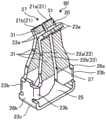
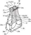
图2是表示图1的一对嵌合构件B的结构的一个例子的示意图。图3是表示图1的一对嵌合构件B的嵌合状态的一个例子的概略剖视图。图2的(a)和图3表示一对嵌合构件B的嵌合状态的一个例子。图2的(b)与图1同样地分别简单地表示雄型嵌合构件Bm和雌型嵌合构件Bf。图2的(c)和图3分别具体地表示雄型嵌合构件Bm和雌型嵌合构件Bf。FIG. 2 is a schematic diagram showing an example of the structure of a pair of fitting members B in FIG. 1 . FIG. 3 is a schematic cross-sectional view showing an example of a fitting state of a pair of fitting members B in FIG. 1 . An example of the fitting state of a pair of fitting members B is shown in FIG.2(a) and FIG.3. (b) of FIG. 2 briefly shows the male type fitting member Bm and the female type fitting member Bf similarly to FIG. 1 . (c) of FIG. 2 and FIG. 3 specifically show the male-type fitting component Bm and the female-type fitting component Bf, respectively.
在电路基板PCB安装的雄型嵌合构件Bm的插入部11向雌型嵌合构件Bf的收容部20插入。具体来说,插入部11一边与第1夹持部21以及第2夹持部22接触,一边以使第1夹持部21与第2夹持部22之间的间隔扩开的方式插入。如图2的(a)和图3所示,通过雌型嵌合构件Bf夹持雄型嵌合构件Bm的插入到第1夹持部21与第2夹持部22之间的插入部11,从而配置有雌型嵌合构件Bf的电路基板PCB和配置有雄型嵌合构件Bm的电路基板PCB结合。此外,将雄型嵌合构件Bm向雌型嵌合构件Bf插入的长度、即插入高度能够根据结合的基板间的距离等来适当地设定。The
图4是表示图1的雄型嵌合构件Bm的结构的一个例子的概略立体图。雄型嵌合构件Bm的插入部11具有大致平板形状的形状。插入部11的前端部13进行了倒角,越朝向前端侧厚度越小。由此,能够容易地将插入部11向雌型嵌合构件Bf的收容部20插入。插入部11的连接部15是插入部11的后端侧的被间隙17分割为3个部分的各个部分。连接部15、即插入部11的后端侧的被分割而成的各个部分相对于插入部11沿大致垂直的方向弯曲。连接部15被焊接于PCB基板上的预定的位置,将插入部11与PCB基板上的配线之间电连接。插入部11和连接部15例如能够通过一张金属的板材的弯曲加工而形成。Fig. 4 is a schematic perspective view showing an example of the structure of the male fitting member Bm in Fig. 1 . The
此外,雄型嵌合构件Bm的插入部11的后端侧的分割数量能够以两个以上的分割数量任意地设计。作为一个例子,插入部11的长度越大,分割数量越大。In addition, the number of divisions of the rear end side of the
图5是表示图1的雌型嵌合构件Bf的结构的一个例子的概略立体图。雌型嵌合构件Bf夹持雄型嵌合构件Bm的插入到收容部20的插入部11。雌型嵌合构件Bf例如通过一张金属的板材的弯曲加工而形成。在从侧面侧、即第1基部26a或第2基部26b那一侧观察时,雌型嵌合构件Bf具有前端侧敞开的大致字母Y状或字母X状的形状。Fig. 5 is a schematic perspective view showing an example of the structure of the female fitting member Bf in Fig. 1 . The female fitting member Bf sandwiches the
具体来说,雌型嵌合构件Bf具有第1夹持部21和第2夹持部22。第1夹持部21和第2夹持部22彼此相对地配置。第1夹持部21的与第2夹持部22相对的面和第2夹持部22的与第1夹持部21相对的面形成收容部20。也就是说,第1夹持部21和第2夹持部22隔着收容部20而相对。雌型嵌合构件Bf夹持雄型嵌合构件Bm的插入到第1夹持部21与第2夹持部22之间的收容部20的插入部11。第1夹持部21在第1弯曲部23a处弯曲成朝向相对的第2夹持部22凸出的形状。同样地,第2夹持部22在第1弯曲部23a处弯曲成朝向相对的第1夹持部21凸出的形状。换言之,第1夹持部21和第2夹持部22分别在第1弯曲部23a处弯曲成朝向彼此相对的面形成凸部。第1夹持部21的第1弯曲部23a和第2夹持部22的第1弯曲部23a隔着收容部20而分离。第1夹持部21的第1弯曲部23a和第2夹持部22的第1弯曲部23a之间的距离比雄型嵌合构件Bm的插入部11的厚度小。Specifically, the female fitting member Bf has a
在第1夹持部21和第2夹持部22,间隙27分别从前端侧设置到后端侧。也就是说,第1夹持部21和第2夹持部22分别被间隙27分割为两部分。换言之,雌型嵌合构件Bf的前端部被间隙27分割为四部分。具体来说,第1夹持部21包括由间隙27分割而成的第1弹性部21a和第2弹性部21b。同样地,第2夹持部22包括由间隙27分割而成的第3弹性部22a和第4弹性部22b。在此,也能够表述为第1弹性部21a和第2弹性部21b隔着间隙27而分离。同样地,也能够表述为第3弹性部22a和第4弹性部22b隔着间隙27而分离。In the
此外,图5示例了由间隙27分割为四部分的雌型嵌合构件Bf,但并不限定于此。由间隙27进行分割的分割数量也可以是5个以上。不过,优选第1夹持部21的分割数量与第2夹持部22的分割数量相等,由间隙27进行分割的分割数量例如是6个以上的偶数。后述的一对嵌合构件B之间的相对的旋转错位有可能在任一方向上产生。因此,通过使第1夹持部21的分割数量与第2夹持部22的分割数量相等,从而不管旋转错位的方向如何,都能够扩大嵌合部的几何学上的容许范围。In addition, although FIG. 5 exemplifies the female-type fitting member Bf divided into four by the
第1弹性部21a和第3弹性部22a分别从第1基部26a延伸设置。换言之,第1弹性部21a和第3弹性部22a分别借助第2弯曲部23b而与第1基部26a连续一体地连结。另外,第2弹性部21b和第4弹性部22b分别从第2基部26b延伸设置。换言之,第2弹性部21b和第4弹性部22b分别借助第2弯曲部23b而与第2基部26b连续一体地连结。另外,第1基部26a和第2基部26b分别从与印刷电路基板连接的连接部25延伸设置。换言之,第1基部26a和第2基部26b分别借助第3弯曲部23c而与连接部25连续一体地连结。The first
因此,第1弹性部21a、第2弹性部21b、第3弹性部22a以及第4弹性部22b分别相当于将第1夹持部21或第2夹持部22分割而成的形状,因此,能够根据与插入部11之间的接触状态而独立地变形。Therefore, the first
此外,实施方式的雄型嵌合构件Bm的插入部11具有大致平板状的形状。另外,实施方式的雌型嵌合构件Bf构成为通过夹持所插入的大致平板形状的插入部11而与雄型嵌合构件Bm嵌合。由此,与例如使用具有销形状的插入部的雄型嵌合构件而实现的基板间连接构造相比较,实施方式的基板间连接构造能够增大一对嵌合构件B之间的接触面积,因此能够降低接触电阻。降低一对嵌合构件B之间的接触电阻有助于抑制一对嵌合构件B的发热、电力损耗、提高与雌型嵌合构件Bf的形状、材料有关的自由度、简化连接状态的判断等。In addition, the
例如,在将销形状的直径和平板形状的厚度设为相同时,由于能够任意地设定平板形状的宽度,因此,平板形状的雄型嵌合构件Bm与相同的长度的销形状的雄型嵌合构件相比,能够增大与雌型嵌合构件Bf之间的接触面积。另外,例如,在将销形状和平板形状的与基板平行的截面的截面面积设为相同时,通过适当地设定平板形状的厚度和宽度,从而能够使平板形状的主面的面积比相同的长度的销形状的表面积大。也就是说,平板形状的雄型嵌合构件Bm与相同的长度的销形状的雄型嵌合构件相比,能够增大与雌型嵌合构件Bf之间的接触面积。For example, when the diameter of the pin shape and the thickness of the flat plate shape are set to be the same, since the width of the flat plate shape can be set arbitrarily, the male fitting member Bm of the flat plate shape and the male pin shape of the same length Compared with the fitting member, the contact area with the female type fitting member Bf can be increased. In addition, for example, when the cross-sectional area of the cross section parallel to the substrate of the pin shape and the flat plate shape is set to be the same, the area ratio of the main surfaces of the flat plate shape can be made the same by appropriately setting the thickness and width of the flat plate shape. The long pin shape has a large surface area. That is, the flat-plate-shaped male fitting member Bm can increase the contact area with the female-type fitting member Bf compared with the pin-shaped male fitting member of the same length.
在此,插入部11的厚度是指图1所示的状态下的插入部11的左右方向上的大小。另外,插入部11的长度是指图1所示的状态下的插入部11的上下方向上的大小。另外,插入部11的宽度是指图1所示的状态下的插入部11的与纸面垂直的方向上的大小。Here, the thickness of the
此外,本公开示例了具有大致平板形状的插入部11的雄型嵌合构件Bm,但不限定于此。例如,雄型嵌合构件Bm也可以具有销形状等大致圆筒形状的插入部11。即使在该情况下,实施方式的雌型嵌合构件Bf的多个弹性部也能够根据与大致圆筒形状的插入部11之间的接触状态而独立地变形。此外,雌型嵌合构件Bf的多个弹性部能够以通过夹持所插入的大致圆筒形状的插入部11而与雄型嵌合构件Bm嵌合的方式配置为例如环状。In addition, the present disclosure exemplifies the male fitting member Bm having the substantially flat plate-shaped
此外,雄型嵌合构件Bm和雌型嵌合构件Bf分别由金属材料形成。作为一个例子,雄型嵌合构件Bm和雌型嵌合构件Bf由铜、包含黄铜在内的铜合金、铝或铝合金形成。In addition, the male fitting member Bm and the female fitting member Bf are each formed of a metal material. As an example, the male fitting member Bm and the female fitting member Bf are formed of copper, copper alloy including brass, aluminum, or an aluminum alloy.
另外,在雄型嵌合构件Bm和雌型嵌合构件Bf的表面区域中的局部或全部区域实施有导体镀敷。例如,导体镀敷实施于在雄型嵌合构件Bm和雌型嵌合构件Bf正常地嵌合时相互接触的区域。作为导体镀敷,例如能够适当地利用镀锡、镀银或镀金。In addition, conductor plating is given to part or all of the surface regions of the male fitting member Bm and the female fitting member Bf. For example, the conductor plating is performed on a region where the male type fitting member Bm and the female type fitting member Bf are normally fitted in contact with each other. As conductor plating, for example, tin plating, silver plating, or gold plating can be suitably used.
在此,锡具有容易与雄型嵌合构件Bm和雌型嵌合构件Bf的基底所使用的镍进行合金化的性质。若周围温度较高,则会进行锡和镍的合金化,电阻值成为1[mΩ]以上。另一方面,银、金不易进行与镍的合金化,但使用成本较高。若雄型嵌合构件Bm与雌型嵌合构件Bf之间的接触电阻较大,则会在雄型嵌合构件Bm与雌型嵌合构件Bf之间的接触部位发生温度上升。因此,在实施方式的电力转换装置1中,将雄型嵌合构件Bm与雌型嵌合构件Bf之间的接触部位处的接触电阻设为1[mΩ]以下。换言之,将一对嵌合构件B嵌合着的状态下的、雄型嵌合构件Bm的插入部11与第1夹持部21或第2夹持部22的凸部之间的接触电阻设为1[mΩ]以下。Here, tin has a property of being easily alloyed with nickel used as a base of the male fitting member Bm and the female fitting member Bf. If the ambient temperature is high, alloying of tin and nickel proceeds, and the resistance value becomes 1 [mΩ] or more. On the other hand, silver and gold are not easy to be alloyed with nickel, but use costs are relatively high. If the contact resistance between the male fitting member Bm and the female fitting member Bf is large, a temperature rise occurs at the contact site between the male fitting member Bm and the female fitting member Bf. Therefore, in the power conversion device 1 of the embodiment, the contact resistance at the contact site between the male fitting member Bm and the female fitting member Bf is set to be 1 [mΩ] or less. In other words, the contact resistance between the
接触电阻的大小由“接触压力(接压)”、“材料(表面的锡等)”以及“接触面积”决定。因此,在实施方式的电力转换装置1中,作为一个例子,通过调整雌型嵌合构件Bf的4个弹性部的弹性力,从而将接触电阻调整成1[mΩ]以下。换言之,实施方式的雌型嵌合构件Bf以使接触电阻成为1[mΩ]以下的方式设计4个弹性部的弹性力。此外,4个弹性部的弹性力例如依赖于雌型嵌合构件Bf的材料(母材)及其形状。The size of the contact resistance is determined by "contact pressure (contact pressure)", "material (tin on the surface, etc.)" and "contact area". Therefore, in the power conversion device 1 of the embodiment, as an example, by adjusting the elastic force of the four elastic portions of the female fitting member Bf, the contact resistance is adjusted to be 1 [mΩ] or less. In other words, in the female fitting member Bf of the embodiment, the elastic forces of the four elastic parts are designed so that the contact resistance becomes 1 [mΩ] or less. In addition, the elastic force of the four elastic parts depends on the material (base material) and shape of the female fitting member Bf, for example.
另外,在本实施方式的雌型嵌合构件Bf设有绝缘部31。绝缘部31设于雌型嵌合构件Bf中的在雄型嵌合构件Bm与雌型嵌合构件Bf正常地嵌合时相互不接触的区域。或者,绝缘部31设于未实施导体镀敷的区域。Moreover, the insulating
作为一个例子,如图5所示,绝缘部31设于雌型嵌合构件Bf的第1夹持部21与第2夹持部22的彼此相对的面和该面的相反侧的面。另一方面,绝缘部31未设置在第1弯曲部23a的鼓出成凸形状的区域、即在嵌合的状态下与雄型嵌合构件Bm接触的区域。As an example, as shown in FIG. 5 , the insulating
作为一个例子,绝缘部31通过雌型嵌合构件Bf的表面处理而形成。例如,绝缘部31是在雌型嵌合构件Bf的表面形成的绝缘体的层(覆膜)。表面处理也可以是对雌型嵌合构件Bf的表面进行的绝缘体的涂布或涂装。作为一个例子,绝缘体是树脂。优选绝缘体是散热绝缘型的树脂。作为散热绝缘型的树脂,例如是散热性较高、即容易放射辐射热的黑色的树脂。或者,表面处理也可以是铝阳极化处理等对雌型嵌合构件Bf的表面进行的散热绝缘型的镀敷处理。在该情况下,绝缘体是在雌型嵌合构件Bf的表面形成的镀敷。另外,作为表面处理,也可以将由绝缘体形成的绝缘膜贴附于雌型嵌合构件Bf的表面。此外,绝缘体的散热性也可以由绝缘体的层、绝缘膜的表面性状来赋予。As an example, the insulating
此外,实施于绝缘部31的表面处理优选为降低一对嵌合构件B之间的摩擦阻力的表面处理。作为一个例子,绝缘部31通过有光泽涂装而形成。在此,有光泽涂装是指涂装面光滑、降低涂装表面的摩擦阻力的涂装。另外,实施于绝缘部31的表面处理优选为增加一对嵌合构件B之间的耐磨耗性的表面处理。在此,增加耐磨耗性的表面处理是指用于降低雄型嵌合构件Bm和雌型嵌合构件Bf摩擦时的磨耗、并且抑制金属污染的产生的表面处理。此外,降低一对嵌合构件B之间的摩擦阻力的表面处理和增加耐磨耗性的表面处理有时例如也能够通过有光泽涂装等共同的表面处理来实现。In addition, it is preferable that the surface treatment given to the insulating
此外,也可以是,由绝缘体形成雌型嵌合构件Bf、或在由导体形成的雌型嵌合构件Bf的整体设置绝缘部31,并且仅对在嵌合的状态下与雄型嵌合构件Bm接触的区域实施导体镀敷(导电部)。也就是说,只要绝缘部31设于未实施导体镀敷的区域即可。或者,也可以是,在由导体形成的雌型嵌合构件Bf的整体设置绝缘体,并且仅对在嵌合的状态下与雄型嵌合构件Bm接触的区域实施去除绝缘体的表面处理。或者,也可以是,由导体形成雌型嵌合构件Bf、或在由绝缘体形成的雌型嵌合构件Bf的整体设置导体镀敷,并且仅对在嵌合的状态下与雄型嵌合构件Bm不接触的区域设置绝缘部31。或者,也可以是,在由绝缘体形成的雌型嵌合构件Bf的整体设置导体,并且实施去除在嵌合的状态下不与雄型嵌合构件Bm接触的区域的导体的表面处理。像这样,绝缘部31有时也能够不形成为绝缘体的层。另外,绝缘部31有时也能够通过用于形成导电部的表面处理而形成为所形成的导电部的其他部分。In addition, it is also possible to form the female-type fitting member Bf from an insulator or provide the insulating
由此,在以下所说明的实施方式的部件间连接的流程中,能够判断部件间连接状态。具体来说,在由于插入部11与收容部20的错位而引起一对雄型嵌合构件Bm和雌型嵌合构件Bf的嵌合产生不良的情况下,能够通过电检查来检测出其连接不良。在此,电检查是指经由雄型嵌合构件Bm与雌型嵌合构件Bf之间的接触部位的电阻值的测量。This makes it possible to determine the connection state between components in the flow of connection between components in the embodiment described below. Specifically, in the event that a pair of male fitting members Bm and female fitting members Bf are poorly fitted due to misalignment between the
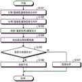
以下,参照附图,对实施方式的部件间连接的流程的一个例子进行说明。图6是表示实施方式的部件间连接的流程的一个例子的流程图。在此,以将设有雄型嵌合构件Bm的第1电路基板PCB1和设有雌型嵌合构件Bf的第2电路基板PCB2结合的情况为例子进行说明。Hereinafter, an example of the flow of connection between components according to the embodiment will be described with reference to the drawings. FIG. 6 is a flowchart showing an example of the flow of connection between components in the embodiment. Here, the case where the 1st circuit board PCB1 provided with the male type fitting member Bm is connected with the 2nd circuit board PCB2 provided with the female type fitting member Bf is demonstrated as an example.
首先,在第1电路基板PCB1的第2基板PCB2侧的主面配置雄型嵌合构件Bm(S101)。另外,在第2基板PCB2的第1电路基板PCB1侧的主面配置雌型嵌合构件Bf(S102)。在一对嵌合构件B分别配置于印刷电路基板上后,例如使用光学式自动外观检查装置(AOI:Automated Optical Inspection)来检查一对嵌合构件B向印刷电路基板上安装的各自的安装状态。在通过该检查而检测到一对嵌合构件B向印刷电路基板上安装的各自的安装状态存在不良的情况下,对于检测到不良的印刷电路基板不实施以后的流程。First, the male fitting member Bm is arranged on the main surface of the first circuit board PCB1 on the second board PCB2 side (S101). Moreover, the female type fitting member Bf is arrange|positioned on the main surface of the 1st circuit board PCB1 side of the 2nd board|substrate PCB2 (S102). After the pair of fitting members B are placed on the printed circuit board, for example, the mounting state of the pair of fitting members B on the printed circuit board is inspected using an automatic optical inspection device (AOI: Automated Optical Inspection). . When it is detected that a pair of fitting members B is defective in the mounting state of each of the printed circuit boards mounted on the printed circuit board by this inspection, the subsequent flow is not performed on the printed circuit board in which the defect was detected.
之后,利用一对嵌合构件B的嵌合,将第1电路基板PCB1与第2基板PCB2结合(S103)。在该步骤中,在由传感器检测到雄型嵌合构件Bm和雌型嵌合构件Bf之间的接触后,将一印刷电路基板向另一印刷基板压入,由此形成层状构造的定置状态。雌型嵌合构件Bf在与雄型嵌合构件Bm的插入部11的插入方向相反的一侧具有弹性力(弹簧力)。因此,当将多个雄型嵌合构件Bm同时向多个雌型嵌合构件Bf压入时,存在若干雄型嵌合构件Bm从雌型嵌合构件Bf的收容部20脱离的情况。因此,在本步骤中,在一旦形成了可靠的嵌合状态之后,进一步将一印刷电路基板向另一印刷基板压入,由此实现良好的嵌合。在此,可靠的嵌合状态是指插入部11向收容部20压入例如1mm左右的稳定状态。After that, the first circuit board PCB1 and the second board PCB2 are joined together by the fitting of the pair of fitting members B (S103). In this step, after the contact between the male fitting member Bm and the female fitting member Bf is detected by the sensor, one printed circuit board is pressed into the other printed board, thereby forming a fixed layered structure. state. The female fitting member Bf has elastic force (spring force) on the side opposite to the insertion direction of the
之后,经由嵌合部测量电阻(S104)。经由嵌合部的电阻的测量例如是第1电路基板PCB1上的与雄型嵌合构件Bm电连接的电路结构的任意的位置和第2基板PCB2上的与雌型嵌合构件Bf电连接的电路结构的任意的位置之间的电阻的测量。After that, resistance is measured via the fitting portion (S104). The measurement of the resistance via the fitting part is, for example, any position of the circuit structure electrically connected to the male fitting member Bm on the first circuit board PCB1 and the position electrically connected to the female fitting member Bf on the second substrate PCB2. Measurement of electrical resistance between arbitrary locations in a circuit structure.
在经由嵌合部的电阻表示为绝缘状态时(S105:Yes),判断该嵌合部为连接不良(S106)。例如,在雄型嵌合构件Bm隔着绝缘部31而与雌型嵌合构件Bf接触时,经由嵌合部的电阻表示为绝缘状态。When the resistance via the fitting portion indicates an insulating state (S105: Yes), it is determined that the fitting portion is poorly connected (S106). For example, when the male fitting member Bm is in contact with the female fitting member Bf via the insulating
另一方面,在经由嵌合部的电阻未表示为绝缘状态时(S105:No),判断该嵌合部为连接良好(S107)。例如,在雄型嵌合构件Bm利用第1弯曲部23a的鼓出成凸形状的区域与雌型嵌合构件Bf接触时,经由嵌合部的电阻不表示为绝缘状态。在步骤S106或S107后,图6的流程结束。On the other hand, when the resistance via the fitting portion does not indicate an insulating state (S105: No), it is determined that the fitting portion is well connected (S107). For example, when the male fitting member Bm is in contact with the female fitting member Bf by the convexly swollen region of the first
像这样,根据使用实施方式的一对嵌合构件B而实现的基板间连接方法,能够抑制将部件间电连接的嵌合部的电连接不良。Thus, according to the inter-substrate connection method realized using the pair of fitting members B of the embodiment, it is possible to suppress poor electrical connection at the fitting portion that electrically connects components.
像上述那样,通过分别安装的雄型嵌合构件Bm和雌型嵌合构件Bf嵌合,从而两个电路基板结合。然而,在将基板尺寸设为同型的情况下等,在组装时视线被电路基板遮挡的情况下,由于目视确认困难,有时无法使嵌合部适当地嵌合。其中,在组装后的状态下嵌合构件彼此接触的情况下,在电检查中无法检测出嵌合部未适当地嵌合的误嵌合件,存在无法抑制部件间的电连接不良的问题。作为以往技术,也有在各嵌合部安装树脂部件等对策,但需要在嵌合部逐个安装树脂部件,不仅成本变高,还存在作业时间增大的问题。As mentioned above, two circuit boards are joined by fitting of the separately attached male type fitting member Bm and female type fitting member Bf. However, when the line of sight is blocked by the circuit board during assembly, such as when the board size is the same type, it may be difficult to make the fitting part fit properly because visual confirmation is difficult. Among them, when the fitting members are in contact with each other in the assembled state, it is impossible to detect a misfit in which the fitting portion is not properly fitted in the electrical inspection, and there is a problem that it is impossible to suppress poor electrical connection between components. As a conventional technique, there are countermeasures such as attaching resin parts to each fitting part, but the resin parts need to be attached to each fitting part one by one, which not only increases the cost, but also has the problem of increasing the working time.
其中,在实施方式的部件间连接构造中,在雌型嵌合构件Bf中的在嵌合时不与雄型嵌合构件Bm接触的区域设有绝缘部31。因此,在误嵌合时在嵌合构件B处能够绝缘,能够通过电检查检测出误嵌合件,因此能够抑制将部件间电连接的嵌合部的电连接不良。Among them, in the inter-part connection structure of the embodiment, the insulating
另外,在实施方式的部件间连接构造中,设于雌型嵌合构件Bf的绝缘部31除了具有绝缘性以外还具有较高的散热性,因此能够提高来自嵌合构件B的散热性。由此,即使在嵌合构件B流动有大电流的情况下,也能够抑制嵌合构件B发热而高温化。In addition, in the inter-component connection structure of the embodiment, the insulating
另外,在实施方式的部件间连接构造中,雌型嵌合构件Bf的供插入部11插入的收容部20具有第1夹持部21和第2夹持部22越朝向前端侧越分离的形状,并且设有通过有光泽涂装而形成的绝缘部31。由此,能够使雄型嵌合构件Bm的插入到收容部20的插入部11滑动地向第1夹持部21和第2夹持部22之间引导。因此,能够抑制在嵌合时雄型嵌合构件Bm无法向第1夹持部21与第2夹持部22之间插入而压坏雌型嵌合构件Bf。另外,绝缘部31从收容部20设置到在嵌合时与雄型嵌合构件Bm接触的区域(接点)附近,因此也能够抑制在插入时雄型嵌合构件Bm和雌型嵌合构件Bf摩擦而产生的金属污染。In addition, in the inter-part connection structure of the embodiment, the
此外,也能够实现如下结构:对第1夹持部21和第2夹持部22的彼此相对的面、即所插入的雄型嵌合构件Bm会接触的面实施有光泽涂装,对相反侧的外周面实施提高散热性的无光泽涂装等。In addition, it is also possible to implement a structure in which glossy coating is applied to the surfaces facing each other of the
以下,一边参照附图,一边对实施方式的部件间连接构造、电力转换装置以及部件间连接方法的各变形例进行说明。此外,在以下的说明中,主要说明与上述的实施方式或各变形例的不同点,适当省略重复的说明。Hereinafter, modifications of the inter-component connection structure, the power conversion device, and the inter-component connection method of the embodiment will be described with reference to the drawings. In addition, in the following description, the difference from the above-mentioned embodiment or each modified example will be mainly described, and the overlapping description will be omitted suitably.
(第1变形例)(1st modified example)
图7是表示图1的雌型嵌合构件Bf的结构的另一个例子的概略立体图。如图7所示,雌型嵌合构件Bf的前端部优选进行边缘去除。边缘去除例如能够通过对雌型嵌合构件Bf的收容部20的边缘进行敲打并将其弄圆、或切削边缘来进行。Fig. 7 is a schematic perspective view showing another example of the structure of the female fitting member Bf of Fig. 1 . As shown in FIG. 7 , it is preferable that the front end portion of the female-type fitting member Bf is edge-cut. Edge removal can be performed, for example, by beating and rounding the edge of the
像这样,在本变形例的部件间连接构造中,对雌型嵌合构件Bf的收容部20、即供雄型嵌合构件Bm的插入部11插入的前端侧的端面实施边缘去除处理来作为去除端面的边缘的端面处理。换言之,在发生误嵌合时等雄型嵌合构件Bm的插入部11会接触的、雌型嵌合构件Bf的前端侧的端面的边缘通过端面处理而被去除。因此,能够抑制雄型嵌合构件Bm被雌型嵌合构件Bf的前端部的边缘切削而产生金属污染。另外,在对雄型嵌合构件Bm实施有涂装的情况下,能够抑制雄型嵌合构件Bm的涂装被切削。In this way, in the inter-part connection structure of this modified example, the receiving
(第2变形例)(Second modified example)
图8是表示图1的雌型嵌合构件Bf的结构的另一个例子的概略立体图。如图8所示,雌型嵌合构件Bf的前端部的端面处理也能够通过前端部的卷曲处理来实现。例如,如图8所示,对第1夹持部21和第2夹持部22分别实施如下这样的卷曲处理来作为端面处理:在供插入部11插入的前端侧,彼此相对的面以分别朝向相反方向的方式向外侧弯折。换言之,雌型嵌合构件Bf的前端侧的端面的边缘不暴露于在发生误嵌合时等雄型嵌合构件Bm的插入部11会接触的、雌型嵌合构件Bf的外侧。即使是该结构,也能够得到与第1变形例同样的效果。另外,根据雌型嵌合构件Bf的前端部的卷曲处理,能够以第1夹持部21和第2夹持部22分别越朝向前端侧越分离的方式形成收容部20,因此能够降低伴随收容部20对插入部11的引入而产生的磨耗,并且容易对与所插入的雄型嵌合构件Bm接触的接触部位进行表面处理。Fig. 8 is a schematic perspective view showing another example of the structure of the female fitting member Bf in Fig. 1 . As shown in FIG. 8 , the end surface treatment of the front end of the female fitting member Bf can also be achieved by crimping the front end. For example, as shown in FIG. 8 , the
此外,上述的各变形例不限定于收容部20,也能够应用于在嵌合时会与雄型嵌合构件Bm接触的其他边缘。另外,上述的各变形例不限定于雌型嵌合构件Bf,也能够应用于前端部13等雄型嵌合构件Bm中的在嵌合时会与雌型嵌合构件Bf接触的边缘。In addition, each modification mentioned above is not limited to the
(第3变形例)(3rd modified example)
图9是表示图1的雄型嵌合构件Bm的结构的另一个例子的概略立体图。图9为了示例嵌合时的位置关系,一并示例雌型嵌合构件Bf。Fig. 9 is a schematic perspective view showing another example of the structure of the male fitting member Bm of Fig. 1 . FIG. 9 also illustrates the female-type fitting member Bf in order to illustrate the positional relationship at the time of fitting.
如图9所示,不限定于雌型嵌合构件Bf,也可以在雄型嵌合构件Bm设置绝缘部32。绝缘部32与绝缘部31同样地,例如利用绝缘体的层、绝缘膜来实现。绝缘部32的绝缘体例如与绝缘部31的绝缘体相同,但也可以不同。设于前端部13的绝缘部32例如通过有光泽涂装来实现。As shown in FIG. 9 , not only the female type fitting member Bf, but also the insulating
雄型嵌合构件Bm的绝缘部32设于雄型嵌合构件Bm中的在雄型嵌合构件Bm与雌型嵌合构件Bf正常嵌合时相互不接触的区域。作为一个例子,如图9所示,绝缘部32设于雄型嵌合构件Bm中的在嵌合时与雌型嵌合构件Bf的第1弯曲部23a的鼓出成凸形状的区域不接触的区域。另一方面,在嵌合时与雌型嵌合构件Bf的第1弯曲部23a的鼓出成凸形状的区域接触的区域设有导电部12。The insulating
例如,导电部12和绝缘部32通过如下方式来实现:由绝缘体形成雄型嵌合构件Bm、或在由导体形成的雄型嵌合构件Bm的整体设置绝缘部32,并且仅对在嵌合的状态下与雌型嵌合构件Bf接触的区域实施导体镀敷。或者,导电部12和绝缘部32通过如下方式来实现:由导体形成雄型嵌合构件Bm、或在由绝缘体形成的雄型嵌合构件Bm的整体设置导体镀敷,并且仅对在嵌合的状态下不与雌型嵌合构件Bf接触的区域设置绝缘部32。For example, the
像这样,在本变形例的部件间连接构造中,在雄型嵌合构件Bm中的在嵌合时不与雌型嵌合构件Bf接触的区域设有绝缘部32。即使是该结构,也能够得到与上述的实施方式以及各变形例同样的效果。另外,嵌合时的插入部11的插入深度由导电部12的位置决定,因此能够抑制半嵌合等不适当的嵌合状态。In this way, in the inter-part connection structure of this modified example, the insulating
此外,上述的实施方式以及各变形例的雄型嵌合构件Bm和雌型嵌合构件Bf分别能够任意地组合。例如,能够将第1变形例或第2变形例的雌型嵌合构件Bf和第3变形例的雄型嵌合构件Bm作为一对嵌合构件B来使用。In addition, the male type fitting member Bm and the female type fitting member Bf of the above-mentioned embodiment and each modified example can be combined arbitrarily. For example, the female fitting member Bf of the first modification or the second modification and the male fitting member Bm of the third modification can be used as a pair of fitting members B. FIG.
像以上说明的那样,根据本公开的部件间连接构造、电力转换装置1以及部件间连接方法,能够抑制将部件间电连接的嵌合部的电连接不良。As described above, according to the inter-component connection structure, the power conversion device 1 , and the inter-component connection method of the present disclosure, it is possible to suppress poor electrical connection at the fitting portion that electrically connects the components.
对本发明的若干实施方式进行了说明,但这些实施方式是作为例子而提出的,意图并不在于限定发明的范围。这些实施方式能够以其他各种各样的方式实施,能够在不脱离发明的主旨的范围内进行各种省略、置换、变更。这些实施方式及其变形包含在发明的范围、主旨内,同样包含在权利要求书所记载的发明及其均等的范围内。Although some embodiments of the present invention have been described, these embodiments are presented as examples and are not intended to limit the scope of the invention. These embodiments can be implemented in other various forms, and various omissions, substitutions, and changes can be made without departing from the scope of the invention. These embodiments and modifications thereof are included in the scope and gist of the invention, and are also included in the invention described in the claims and their equivalents.
Claims (7)
Translated fromChineseApplications Claiming Priority (2)
| Application Number | Priority Date | Filing Date | Title |
|---|---|---|---|
| JP2021124750AJP7609526B2 (en) | 2021-07-29 | 2021-07-29 | Inter-component connection structure, power conversion device, and inter-component connection method |
| JP2021-124750 | 2021-07-29 |
Publications (1)
| Publication Number | Publication Date |
|---|---|
| CN115693320Atrue CN115693320A (en) | 2023-02-03 |
Family
ID=84890039
Family Applications (1)
| Application Number | Title | Priority Date | Filing Date |
|---|---|---|---|
| CN202210896502.1APendingCN115693320A (en) | 2021-07-29 | 2022-07-28 | Connection structure between members |
Country Status (4)
| Country | Link |
|---|---|
| US (1) | US20230034324A1 (en) |
| JP (1) | JP7609526B2 (en) |
| CN (1) | CN115693320A (en) |
| DE (1) | DE102022117568A1 (en) |
Family Cites Families (13)
| Publication number | Priority date | Publication date | Assignee | Title |
|---|---|---|---|---|
| JPH0745329A (en)* | 1993-08-02 | 1995-02-14 | Nitsupo Denki Kk | Plug-in connector |
| JPH0850946A (en)* | 1994-08-04 | 1996-02-20 | Yazaki Corp | Busbar connection device for electrical junction box |
| JP3045111U (en)* | 1997-07-07 | 1998-01-23 | 智 伊藤 | Outlet plug coated at the root |
| US6416342B2 (en)* | 1998-12-10 | 2002-07-09 | Advantest Corporation | Socket and connector therefor for connecting with an electrical component |
| JP2006032113A (en)* | 2004-07-15 | 2006-02-02 | Kawaguchi:Kk | Wire connector |
| JP4488915B2 (en)* | 2005-01-26 | 2010-06-23 | 本多通信工業株式会社 | Optical connector |
| JP5334818B2 (en)* | 2009-11-30 | 2013-11-06 | 日立電線株式会社 | Connection structure |
| JP2012003913A (en)* | 2010-06-16 | 2012-01-05 | Japan Aviation Electronics Industry Ltd | connector |
| JP2012151226A (en) | 2011-01-18 | 2012-08-09 | Toyota Industries Corp | Inter-substrate connection structure |
| CN105075023B (en)* | 2013-02-18 | 2017-08-29 | 株式会社自动网络技术研究所 | Electric connection structure and terminal |
| CN106165203B (en)* | 2014-04-03 | 2019-02-15 | 株式会社自动网络技术研究所 | Terminal Pairs and Connector Pairs with Terminal Pairs |
| JP6694610B2 (en)* | 2016-06-27 | 2020-05-20 | 日本圧着端子製造株式会社 | connector |
| JP6622252B2 (en)* | 2017-06-09 | 2019-12-18 | 矢崎総業株式会社 | Connector device |
- 2021
- 2021-07-29JPJP2021124750Apatent/JP7609526B2/enactiveActive
- 2022
- 2022-07-14DEDE102022117568.5Apatent/DE102022117568A1/enactivePending
- 2022-07-21USUS17/870,666patent/US20230034324A1/enactivePending
- 2022-07-28CNCN202210896502.1Apatent/CN115693320A/enactivePending
Also Published As
| Publication number | Publication date |
|---|---|
| JP2023019777A (en) | 2023-02-09 |
| JP7609526B2 (en) | 2025-01-07 |
| US20230034324A1 (en) | 2023-02-02 |
| DE102022117568A1 (en) | 2023-02-02 |
Similar Documents
| Publication | Publication Date | Title |
|---|---|---|
| US9391385B2 (en) | Dual compressive connector | |
| EP2797189B1 (en) | Electromagnetic shielding tool and wire harness | |
| CN103515730B (en) | Without cage adapter | |
| US8979602B2 (en) | Electrical male terminal | |
| WO2014170957A1 (en) | Bus bar | |
| US20140017940A1 (en) | Layered connector and method of manufacturing a layered connector | |
| EP2963739B1 (en) | Dual thickness double-ended male blade terminal and method of manufacturing it | |
| JP2025036487A (en) | Power Conversion Equipment | |
| JP7614699B2 (en) | Power Conversion Equipment | |
| JP2025075044A (en) | Power conversion device, component connection system, and component connection method | |
| CN115693320A (en) | Connection structure between members | |
| EP4435814A1 (en) | Electronic component mounting module having bus bar stack, and method for manufacturing same | |
| JP7153883B1 (en) | Power conversion device and board-to-board connection | |
| EP4343976A1 (en) | Electric power converting device, and board-to-board connecting portion | |
| JP7182112B1 (en) | Power conversion device and board-to-board connection | |
| EP4492584A1 (en) | Electrical connection assembly | |
| JP2011187167A (en) | Connection terminal for thin plate laminated conductor, connection structure for thin plate laminated conductor, and connection method for thin plate laminated conductor | |
| CN103490198B (en) | Female fuse terminal and the printed circuit-board assembly for female fuse terminal | |
| JP2017126411A (en) | Terminal, electric wire with terminal, and method of manufacturing electric wire with terminal | |
| CN115332852A (en) | An electrical connector contact piece suitable for ultrasonic welding | |
| TWM448058U (en) | Junction box | |
| JP2018181720A (en) | Flexible flat cable and method of manufacturing the same | |
| CN114730756A (en) | semiconductor device |
Legal Events
| Date | Code | Title | Description |
|---|---|---|---|
| PB01 | Publication | ||
| PB01 | Publication | ||
| SE01 | Entry into force of request for substantive examination | ||
| SE01 | Entry into force of request for substantive examination | ||
| TA01 | Transfer of patent application right | Effective date of registration:20240328 Address after:Kanagawa Prefecture, Japan Applicant after:Panasonic Automotive Electronic Systems Co.,Ltd. Country or region after:Japan Address before:Osaka, Japan Applicant before:PANASONIC INTELLECTUAL PROPERTY MANAGEMENT Co.,Ltd. Country or region before:Japan | |
| TA01 | Transfer of patent application right |