CN115692263B - Semiconductor process chamber and semiconductor process equipment - Google Patents
Semiconductor process chamber and semiconductor process equipmentDownload PDFInfo
- Publication number
- CN115692263B CN115692263BCN202211347495.6ACN202211347495ACN115692263BCN 115692263 BCN115692263 BCN 115692263BCN 202211347495 ACN202211347495 ACN 202211347495ACN 115692263 BCN115692263 BCN 115692263B
- Authority
- CN
- China
- Prior art keywords
- insulator
- sub
- axis
- interface
- semiconductor process
- Prior art date
- Legal status (The legal status is an assumption and is not a legal conclusion. Google has not performed a legal analysis and makes no representation as to the accuracy of the status listed.)
- Active
Links
Images


Classifications
- H—ELECTRICITY
- H01—ELECTRIC ELEMENTS
- H01L—SEMICONDUCTOR DEVICES NOT COVERED BY CLASS H10
- H01L21/00—Processes or apparatus adapted for the manufacture or treatment of semiconductor or solid state devices or of parts thereof
- H01L21/67—Apparatus specially adapted for handling semiconductor or electric solid state devices during manufacture or treatment thereof; Apparatus specially adapted for handling wafers during manufacture or treatment of semiconductor or electric solid state devices or components ; Apparatus not specifically provided for elsewhere
- H01L21/67005—Apparatus not specifically provided for elsewhere
- H01L21/67011—Apparatus for manufacture or treatment
- H01L21/67017—Apparatus for fluid treatment
- H01L21/67063—Apparatus for fluid treatment for etching
- H01L21/67069—Apparatus for fluid treatment for etching for drying etching
- H—ELECTRICITY
- H01—ELECTRIC ELEMENTS
- H01J—ELECTRIC DISCHARGE TUBES OR DISCHARGE LAMPS
- H01J31/00—Cathode ray tubes; Electron beam tubes
- H01J31/08—Cathode ray tubes; Electron beam tubes having a screen on or from which an image or pattern is formed, picked up, converted, or stored
- H01J31/26—Image pick-up tubes having an input of visible light and electric output
- H01J31/28—Image pick-up tubes having an input of visible light and electric output with electron ray scanning the image screen
- H01J31/30—Image pick-up tubes having an input of visible light and electric output with electron ray scanning the image screen having regulation of screen potential at anode potential, e.g. iconoscope
- H01J31/32—Tubes with image amplification section, e.g. image-iconoscope, supericonoscope
- H—ELECTRICITY
- H01—ELECTRIC ELEMENTS
- H01J—ELECTRIC DISCHARGE TUBES OR DISCHARGE LAMPS
- H01J37/00—Discharge tubes with provision for introducing objects or material to be exposed to the discharge, e.g. for the purpose of examination or processing thereof
- H01J37/32—Gas-filled discharge tubes
- H—ELECTRICITY
- H01—ELECTRIC ELEMENTS
- H01J—ELECTRIC DISCHARGE TUBES OR DISCHARGE LAMPS
- H01J37/00—Discharge tubes with provision for introducing objects or material to be exposed to the discharge, e.g. for the purpose of examination or processing thereof
- H01J37/32—Gas-filled discharge tubes
- H01J37/32431—Constructional details of the reactor
- H01J37/32532—Electrodes
- H01J37/32541—Shape
- H—ELECTRICITY
- H01—ELECTRIC ELEMENTS
- H01L—SEMICONDUCTOR DEVICES NOT COVERED BY CLASS H10
- H01L21/00—Processes or apparatus adapted for the manufacture or treatment of semiconductor or solid state devices or of parts thereof
- H01L21/67—Apparatus specially adapted for handling semiconductor or electric solid state devices during manufacture or treatment thereof; Apparatus specially adapted for handling wafers during manufacture or treatment of semiconductor or electric solid state devices or components ; Apparatus not specifically provided for elsewhere
- H01L21/683—Apparatus specially adapted for handling semiconductor or electric solid state devices during manufacture or treatment thereof; Apparatus specially adapted for handling wafers during manufacture or treatment of semiconductor or electric solid state devices or components ; Apparatus not specifically provided for elsewhere for supporting or gripping
- Y—GENERAL TAGGING OF NEW TECHNOLOGICAL DEVELOPMENTS; GENERAL TAGGING OF CROSS-SECTIONAL TECHNOLOGIES SPANNING OVER SEVERAL SECTIONS OF THE IPC; TECHNICAL SUBJECTS COVERED BY FORMER USPC CROSS-REFERENCE ART COLLECTIONS [XRACs] AND DIGESTS
- Y02—TECHNOLOGIES OR APPLICATIONS FOR MITIGATION OR ADAPTATION AGAINST CLIMATE CHANGE
- Y02P—CLIMATE CHANGE MITIGATION TECHNOLOGIES IN THE PRODUCTION OR PROCESSING OF GOODS
- Y02P70/00—Climate change mitigation technologies in the production process for final industrial or consumer products
- Y02P70/50—Manufacturing or production processes characterised by the final manufactured product
Landscapes
- Engineering & Computer Science (AREA)
- Physics & Mathematics (AREA)
- Microelectronics & Electronic Packaging (AREA)
- Condensed Matter Physics & Semiconductors (AREA)
- General Physics & Mathematics (AREA)
- Manufacturing & Machinery (AREA)
- Computer Hardware Design (AREA)
- Power Engineering (AREA)
- Chemical & Material Sciences (AREA)
- Analytical Chemistry (AREA)
- Plasma & Fusion (AREA)
- Drying Of Semiconductors (AREA)
- Plasma Technology (AREA)
Abstract
Description
Translated fromChinese技术领域technical field
本申请属于半导体装备技术领域,具体涉及一种半导体工艺腔室及半导体工艺设备。The application belongs to the technical field of semiconductor equipment, and in particular relates to a semiconductor process chamber and semiconductor process equipment.
背景技术Background technique
随着半导体工艺制程的发展,对半导体刻蚀工艺的均匀性越来越高。半导体刻蚀工艺设备,如,ICP刻蚀设备中,上电极的线圈通过感应耦合的方式在腔室内部产生等离子体,同时,在下电极上施加一定频率的射频功率,射频功率通过容性耦合的方式作用于晶圆表面的等离子体,从而控制到达晶圆表面的离子能量。高能离子轰击晶圆表面破坏刻蚀过程中产生的对刻蚀反应起阻挡作用的CF膜等,从而加快刻蚀速率。With the development of the semiconductor process, the uniformity of the semiconductor etching process is getting higher and higher. Semiconductor etching process equipment, for example, in ICP etching equipment, the coil of the upper electrode generates plasma inside the chamber through inductive coupling, and at the same time, a certain frequency of radio frequency power is applied to the lower electrode, and the radio frequency power is passed through capacitively coupled The method acts on the plasma on the wafer surface, thereby controlling the ion energy reaching the wafer surface. High-energy ions bombard the surface of the wafer to destroy the CF film that blocks the etching reaction during the etching process, thereby accelerating the etching rate.
基于上述内容可知,影响刻蚀工艺均匀性的主要因素包括:晶圆表面的等离子体均匀性,下电极回路控制的离子能量分布均匀性、达到晶圆表面的刻蚀反应物的密度分布均匀性等。下电极回路的对称性是决定刻蚀工艺均匀性的一个重要因素,然而,一些刻蚀设备中,由于元件(如,传片口、排气口、悬臂等)几何结构存在不对称性,因此,会对刻蚀的均匀性产生较大影响。Based on the above, it can be seen that the main factors affecting the uniformity of the etching process include: the uniformity of the plasma on the wafer surface, the uniformity of the ion energy distribution controlled by the lower electrode circuit, and the uniformity of the density distribution of the etching reactants reaching the wafer surface. wait. The symmetry of the lower electrode circuit is an important factor that determines the uniformity of the etching process. However, in some etching equipment, due to the asymmetry of the geometric structure of the components (such as the transfer port, exhaust port, cantilever, etc.), therefore, It will have a great influence on the uniformity of etching.
发明内容Contents of the invention
本申请实施例的目的是提供一种半导体工艺腔室及半导体工艺设备,能够解决当前刻蚀设备中元件几何结构不对称而影响刻蚀均匀性等问题。The purpose of the embodiments of the present application is to provide a semiconductor process chamber and semiconductor process equipment, which can solve the problems of the current etching equipment, such as the asymmetry of the geometric structure of the element, which affects the etching uniformity.
为了解决上述技术问题,本申请是这样实现的:In order to solve the above-mentioned technical problems, the application is implemented as follows:
本申请实施例提供了一种半导体工艺腔室,包括:腔体、内衬和下电极结构,所述内衬和所述下电极结构均设置于所述腔体内;An embodiment of the present application provides a semiconductor process chamber, including: a chamber body, a liner, and a lower electrode structure, and the inner liner and the lower electrode structure are both arranged in the chamber;
所述下电极结构包括基座、接口件、承载件、射频馈入件和屏蔽件;所述承载件用于承载晶圆;The lower electrode structure includes a base, an interface part, a carrier part, a radio frequency feed-in part and a shielding part; the carrier part is used to carry a wafer;
所述基座通过悬臂与所述腔体的侧壁连接;The base is connected to the side wall of the cavity through a cantilever;
所述接口件和所述承载件沿第一方向依次叠置于所述基座;The interface part and the carrier part are sequentially stacked on the base along the first direction;
所述内衬环设于所述下电极结构的外侧,所述内衬的一端与所述腔体电连接,所述内衬的另一端与所述接口件电连接;The inner lining ring is arranged on the outer side of the lower electrode structure, one end of the inner lining is electrically connected to the cavity, and the other end of the inner lining is electrically connected to the interface member;
所述屏蔽件的第一端连接至所述接口件,所述屏蔽件的第二端连接至所述基座的内壁;所述屏蔽件的第一端的轴线与所述接口件的轴线不重合,且所述屏蔽件的第一端的轴线向远离所述悬臂的方向偏移;The first end of the shielding part is connected to the interface part, and the second end of the shielding part is connected to the inner wall of the base; the axis of the first end of the shielding part is different from the axis of the interface part coincident, and the axis of the first end of the shielding member is offset in a direction away from the cantilever;
所述射频馈入件穿设于所述屏蔽件内,且沿所述第一方向穿过所述接口件后与所述承载件连接,用于向所述承载件馈入射频功率。The radio frequency feed-in part is disposed in the shielding part, passes through the interface part along the first direction, and is connected to the carrier part, so as to feed radio frequency power into the carrier part.
本申请实施例还提供了一种半导体工艺设备,包括上述半导体工艺腔室。The embodiment of the present application also provides a semiconductor process equipment, including the above-mentioned semiconductor process chamber.
本申请实施例中,承载件用于承载待刻蚀的晶圆,射频馈入件连接至承载件,用于向承载件馈入射频功率,通过射频功率作用于晶圆表面的等离子体,以控制到达晶圆表面的离子能量,屏蔽件套设于射频馈入件的外侧,起到屏蔽作用,可以减少能量损耗;屏蔽件的第一端连接至接口件,屏蔽件的第二端连接至基座的内壁,屏蔽件的第一端的轴线与接口件的轴线不重合,且屏蔽件的第一端的轴线向远离悬臂的方向偏移,从而可以补偿半导体工艺腔室中固有的元件几何分布不对称性引起的下电极回路的不对称性,进而可以使电极回路中电流密度更均匀,以提高刻蚀工艺的均匀性。In the embodiment of the present application, the carrier is used to carry the wafer to be etched, and the radio frequency feed-in member is connected to the carrier for feeding radio frequency power to the carrier, and the radio frequency power acts on the plasma on the surface of the wafer to To control the ion energy reaching the surface of the wafer, the shielding piece is set outside the RF feed-in piece to play a shielding role and reduce energy loss; the first end of the shielding piece is connected to the interface piece, and the second end of the shielding piece is connected to the The inner wall of the base, the axis of the first end of the shielding part does not coincide with the axis of the interface part, and the axis of the first end of the shielding part is offset in the direction away from the cantilever, so that the inherent element geometry in the semiconductor process chamber can be compensated The asymmetry of the lower electrode circuit caused by the asymmetric distribution can make the current density in the electrode circuit more uniform, so as to improve the uniformity of the etching process.
附图说明Description of drawings
图1为本申请实施例公开的半导体工艺腔室的结构示意图;FIG. 1 is a schematic structural diagram of a semiconductor process chamber disclosed in an embodiment of the present application;
图2为本申请实施例公开的下电极结构的结构示意图;FIG. 2 is a schematic structural diagram of the lower electrode structure disclosed in the embodiment of the present application;
图3为本申请实施例公开的射频馈入件与承载件的相对位置关系示意图;Fig. 3 is a schematic diagram of the relative positional relationship between the RF feed-in part and the carrier part disclosed in the embodiment of the present application;
图4为本申请实施例公开的接口件、屏蔽件、第二绝缘件、射频馈入件、悬臂及匹配器等结构的相对位置关系示意图;Fig. 4 is a schematic diagram of the relative positional relationship of the interface, shielding, second insulator, radio frequency feed-in, cantilever and matching device disclosed in the embodiment of the present application;
图5为本申请实施例公开的屏蔽件、射频馈入件及其中一种形式的第二绝缘件的相对位置关系示意图;Fig. 5 is a schematic diagram of the relative positional relationship between the shielding part, the radio frequency feed-in part and one form of the second insulating part disclosed in the embodiment of the present application;
图6为本申请实施例公开的屏蔽件、射频馈入件及另一种形式的第二绝缘件的相对位置关系示意图;Fig. 6 is a schematic diagram of the relative positional relationship between the shielding part, the radio frequency feed-in part and another form of the second insulating part disclosed in the embodiment of the present application;
图7为本申请实施例公开的第一距离与第二距离的距离差为10mm时半导体工艺腔室两侧电流密度分布曲线;Fig. 7 is the current density distribution curve on both sides of the semiconductor process chamber when the distance difference between the first distance and the second distance disclosed in the embodiment of the present application is 10 mm;
图8为本申请实施例公开的第二子绝缘件为树脂情况下,在第一距离和第二距离的距离差为50mm和100mm条件下的半导体工艺腔室两侧归一化电流密度分布曲线;Fig. 8 is the normalized current density distribution curve on both sides of the semiconductor process chamber under the condition that the distance difference between the first distance and the second distance is 50mm and 100mm when the second sub-insulator disclosed in the embodiment of the present application is resin ;
图9为本申请实施例公开的第二子绝缘件为空气情况下,在第一距离和第二距离的距离差为50mm和100mm条件下的半导体工艺腔室两侧归一化电流密度分布曲线。Fig. 9 is the normalized current density distribution curve on both sides of the semiconductor process chamber under the condition that the distance difference between the first distance and the second distance is 50 mm and 100 mm when the second sub-insulator disclosed in the embodiment of the present application is air .
附图标记说明:Explanation of reference signs:
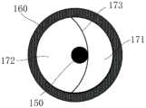
100-下电极结构;110-基座;111-第一侧壁;120-接口件;121-通孔;130-第一绝缘件;140-承载件;150-射频馈入件;160-屏蔽件;170-第二绝缘件;171-第一子绝缘件;172-第二子绝缘件;173-分界面;100-lower electrode structure; 110-base; 111-first side wall; 120-interface; 121-through hole; 130-first insulating part; Part; 170-the second insulating part; 171-the first sub-insulating part; 172-the second sub-insulating part; 173-interface;
200-内衬;200-lining;
300-接地环;300-grounding ring;
400-腔体;400-cavity;
500-悬臂;500-cantilever;
600-匹配器;600 - matcher;
a-第一距离;b-第二距离;e-第三距离;f-第四距离。a-first distance; b-second distance; e-third distance; f-fourth distance.
具体实施方式Detailed ways
下面将结合本申请实施例中的附图,对本申请实施例中的技术方案进行清楚、完整地描述,显然,所描述的实施例是本申请一部分实施例,而不是全部的实施例。基于本申请中的实施例,本领域普通技术人员在没有作出创造性劳动前提下所获得的所有其他实施例,都属于本申请保护的范围。The following will clearly and completely describe the technical solutions in the embodiments of the present application with reference to the drawings in the embodiments of the present application. Obviously, the described embodiments are part of the embodiments of the present application, not all of them. Based on the embodiments in this application, all other embodiments obtained by persons of ordinary skill in the art without creative efforts fall within the protection scope of this application.
本申请的说明书和权利要求书中的术语“第一”、“第二”等是用于区别类似的对象,而不用于描述特定的顺序或先后次序。应该理解这样使用的数据在适当情况下可以互换,以便本申请的实施例能够以除了在这里图示或描述的那些以外的顺序实施,且“第一”、“第二”等所区分的对象通常为一类,并不限定对象的个数,例如第一对象可以是一个,也可以是多个。此外,说明书以及权利要求中“和/或”表示所连接对象的至少其中之一,字符“/”,一般表示前后关联对象是一种“或”的关系。The terms "first", "second" and the like in the specification and claims of the present application are used to distinguish similar objects, and are not used to describe a specific sequence or sequence. It should be understood that the terms so used are interchangeable under appropriate circumstances such that the embodiments of the application can be practiced in sequences other than those illustrated or described herein, and that references to "first," "second," etc. distinguish Objects are generally of one type, and the number of objects is not limited. For example, there may be one or more first objects. In addition, "and/or" in the specification and claims means at least one of the connected objects, and the character "/" generally means that the related objects are an "or" relationship.
下面结合附图,通过具体的实施例及其应用场景对本申请实施例进行详细地说明。The following describes the embodiments of the present application in detail through specific embodiments and application scenarios in conjunction with the accompanying drawings.
相关技术的电极结构中,射频功率由射频源、射频匹配器产生,通过射频连接柱从静电卡盘的中心馈入,然而,射频连接柱、静电卡盘、绝缘环、接口盘、屏蔽套筒等元件均采用同心设置,由于存在悬臂,使得腔室本身并不是完全几何对称的,导致悬臂侧和其对侧的电流路径存在差异。具体地,射频匹配器侧的电流回路中,内衬上的电流与屏蔽套筒上的电流方向相反,存在磁场抵消效应,导致射频匹配器侧的回路电感比其对侧的回路电感要小,从而导致两侧的电流不对称,影响刻蚀工艺的均匀性。In the electrode structure of the related art, the radio frequency power is generated by the radio frequency source and the radio frequency matching device, and is fed from the center of the electrostatic chuck through the radio frequency connecting post, however, the radio frequency connecting post, the electrostatic chuck, the insulating ring, the interface plate, the shielding sleeve The components are concentrically arranged. Due to the existence of the cantilever, the chamber itself is not completely geometrically symmetrical, resulting in a difference in the current path between the cantilever side and its opposite side. Specifically, in the current loop on the side of the RF matcher, the direction of the current on the lining is opposite to that on the shielding sleeve, and there is a magnetic field cancellation effect, resulting in a smaller loop inductance on the side of the RF matcher than on the opposite side. As a result, the currents on both sides are asymmetrical, which affects the uniformity of the etching process.
为了解决上述问题,本申请实施例公开了一种改进后的半导体工艺腔室,综合考虑到几何元件的不对称性对于电流的影响,从而可以有效解决电流的不对称性,确保刻蚀工艺的均匀性。In order to solve the above problems, the embodiment of the present application discloses an improved semiconductor process chamber, which can effectively solve the asymmetry of the current and ensure the accuracy of the etching process by comprehensively considering the influence of the asymmetry of the geometric elements on the current. Uniformity.
参考图1至图9,所公开的半导体工艺腔室包括腔体400、内衬200和下电极结构100。其中,内衬200和下电极结构100均设置于腔体400内,下电极结构100包括基座110、接口件120、承载件140、射频馈入件150和屏蔽件160。除此以外,下电极结构100还可以包括其他元件,以保证下电极结构100的正常使用。Referring to FIGS. 1 to 9 , the disclosed semiconductor process chamber includes a
其中,内衬200环设于下电极结构100的外侧,且内衬200的一端与腔体400电连接,内衬200的另一端与接口件120电连接,如此,通过内衬200可以实现接口件120与腔体400之间的电导通。Wherein, the
基座110为下电极结构100的基础安装构件,其可以为接口件120、承载件140、屏蔽件160等构件提供支撑基础,一些实施例中,基座110可以通过悬臂500与腔体400的侧壁连接,如此,可以通过悬臂500实现对基座110的安装和支撑。The
承载件140用于承载晶圆,接口件120用于连接屏蔽件160,还可以支撑承载件140。一些实施例中,接口件120和承载件140沿第一方向依次叠置于基座110。在实际使用的工况下,接口件120可以安装在基座110的顶部,承载件140可以安装在接口件120的顶部,从而可以通过基座110对接口件120起到支撑作用,并且通过接口件120支撑承载件140。其中,上述第一方向可以理解为,在实际使用工况下自下至上的方向,如图2所示。The
示例性地,承载件140可以为承载盘,即,静电卡盘。优选地,承载盘可以为圆盘件,其具有承载面,以通过承载面承载待刻蚀的晶圆。另外,承载件140可以使馈入的射频功率作用于晶圆表面的等离子体,以控制等离子体到达晶圆表面的离子能量。Exemplarily, the
接口件120可以为接口盘,示例性地,接口盘可以为圆盘件,其可以为屏蔽件160提供安装基础,保证屏蔽件160的安装稳定性。另外,接口盘可以设有开口,以便于使射频馈入件150穿过。The
屏蔽件160的第一端连接至接口件120,屏蔽件160的第二端连接至基座110的内壁;射频馈入件150穿设于屏蔽件160内,且沿第一方向穿过接口件120后与承载件140连接,用于向承载件140馈入射频功率。基于此,通过将屏蔽件160套设在射频馈入件150的外侧,可以对位于基座110的腔体内的射频馈入件150的一段进行遮挡,以实现屏蔽效果,有效缓解能量损耗,在一定程度上可以降低对刻蚀工艺的影响。The first end of the shielding
为了适应射频馈入件150的形状,屏蔽件160可以为屏蔽筒,具体地,屏蔽件160可以包括相连或一体设置的直筒段和弯筒段,其中,弯筒段的背离直筒段的端部即为屏蔽件160的第一端,而直筒段的背离弯筒段的端部即为屏蔽件160的第二端。基于此,通过屏蔽件160可对射频馈入件150的穿入基座110的部分进行遮挡,以起到屏蔽作用。In order to adapt to the shape of the RF feed-in
此处需要说明的是,射频馈入件150用于与匹配器600连接,而匹配器600设置在腔体400外部的一侧,使得匹配器600同样位于下电极结构100的一侧,如此,本申请实施例中,可以将基座110的靠近匹配器600(或靠近悬臂500)的侧壁定义为第一侧壁111。It should be noted here that the RF feed-through 150 is used to connect with the
为了使射频馈入件150穿入基座110,可以在基座110的第一侧壁111设置开口,以使射频馈入件150经由开口进入到基座110的腔体内,并依次穿过接口件120朝向承载件140延伸,最终与承载件140实现连接,以便于将射频源、匹配器600产生的射频功率传输至承载件140,从而控制到达承载于承载件140的晶圆表面的离子能量。In order to allow the RF feed-in
本申请实施例中,通过悬臂500将下电极结构100固定至腔体400内,保证了下电极结构100安装的牢固性和稳定性。示例性地,悬臂500可以设有悬臂通道,屏蔽件160可以在穿出第一侧壁111后穿入至悬臂通道中,最终与腔体400的侧壁连接,如此,可以对位于基座110的第一侧壁111与腔体400的侧壁之间的射频馈入件150的一段进行遮挡,实现屏蔽效果,有效缓解能量损耗,在一定程度上可以降低对刻蚀工艺的影响;另外,悬臂通道主要用于连接外部的线缆和管路,且还用于实现和腔体400接地,以形成电回路。In the embodiment of the present application, the
考虑到由于悬臂500等元件的存在,以及射频馈入件150从悬臂500(或匹配器600)所在的一侧,导致下电极结构100的几何结构在靠近悬臂500的一侧和远离悬臂500的一侧存在不对称性,从而导致该下电极结构100在靠近悬臂500的一侧和远离悬臂500的一侧各自的回路中的电流密度存在差异,进而会影响刻蚀的均匀性。Considering that due to the existence of elements such as the
基于上述情况,本申请实施例中,屏蔽件160的第一端的轴线与接口件120的轴线不重合,且屏蔽件160的第一端的轴线向远离悬臂500的方向偏离,以增加该侧的电感,用以调节下电极回路两侧的阻抗。基于此,可以补偿半导体工艺腔室中固有的元件几何分布不对称性引起的下电极回路的不对称性,进而可以使电极回路中电流密度更均匀,以提高刻蚀工艺的均匀性。Based on the above, in the embodiment of the present application, the axis of the first end of the shielding
在一些实施例中,射频馈入件150的馈入端的轴线与屏蔽件160的第一端的轴线不重合,且射频馈入件150的馈入端的轴线向靠近悬臂500的方向偏移。如图4所示,射频馈入件150与屏蔽件160属于非同心结构,屏蔽件160的第一端的轴线到第一侧壁111的距离比射频馈入件150的馈入端的轴线到第一侧壁111的距离更大。具体地,另屏蔽件160的第一端的靠近第一侧壁111的一侧至射频馈入件150的轴线的距离为第三距离e,屏蔽件160的第一端的远离第一侧壁111的一侧至射频馈入件150的轴线的距离为第四距离f,且第三距离e小于第四距离f。In some embodiments, the axis of the feeding end of the
进一步地,射频馈入件150的馈入端的轴线位于屏蔽件160的第一端的轴线与接口件120的轴线之间。Further, the axis of the feed-in end of the RF feed-in
基于上述设置,可以使靠近悬臂500的一侧与远离悬臂的一侧各自回路中的电感得以调整,使得两侧回路中的电流密度同样受到调整,从而可以使靠近匹配器侧的回路中的电流密度与远离匹配器侧的回路中的电流密度对称,进而可以保证刻蚀工艺的均匀性。Based on the above settings, the inductance in the loops on the side close to the
参考图2,由于射频馈入件150穿过接口件120,为了对射频馈入件150进行绝缘处理,下电极结构100还可以包括第二绝缘件170,相应地,接口件120可以设有通孔121,第二绝缘件170设置于该通孔121中,射频馈入件150穿过第二绝缘件170。基于此,通过设置通孔121可以为第二绝缘件170提供安装空间,并且,通过第二绝缘件170可以使射频馈入件150与接口件120分隔开,以实现对射频馈入件150的绝缘处理。Referring to FIG. 2 , since the RF feed-in
进一步地,屏蔽件160的第一端连接至接口件120的通孔121处,且屏蔽件160的第一端处的轴线与第二绝缘件170的轴线共线,此时,通孔121的轴线、屏蔽件160的轴线以及第二绝缘件170的轴线三者共线。然而,由于射频馈入件150的馈入端的轴线与屏蔽件160的轴线不共线,使得射频馈入件150的馈入端的轴线与第二绝缘件170的轴线同样不共线。具体地,第二绝缘件170在射频馈入件150的靠近悬臂500的一侧部分的宽度尺寸,小于第二绝缘件170在射频馈入件150的远离悬臂500的一侧部分的宽度尺寸,以确保接口件120与屏蔽件160之间的装配性,并且方便于射频馈入件150的装配。Further, the first end of the shielding
为了适应射频馈入件150的安装,通孔121可以设置在接口件120的偏向远离悬臂500一侧的位置,也即,通孔121的轴线位于接口件120的轴线的远离悬臂500的一侧,从而可以通过其内安装的第二绝缘件170适应于对射频馈入件150的安装,以防止各元件之间出现装配干涉。In order to adapt to the installation of the RF feed-in
另外,接口件120的靠近悬臂500的一侧至通孔121的轴线的距离为第五距离,接口件120的远离悬臂500的一侧至通孔121的轴线的距离为第六距离,且第五距离大于第六距离,也即,接口件120的靠近悬臂500一侧部分的宽度尺寸大于远离悬臂500一侧部分的宽度尺寸,以便于适应射频馈入件150的安装。此处需要说明的是,第五距离与第六距离的距离差取决于射频馈入件150的偏心量、第二绝缘件170的偏心量,实际设计时,需确保接口件120与屏蔽件160的装配性即可。In addition, the distance from the side of the
参考图4至图6,在一些实施例中,第二绝缘件170可以包括相适配的第一子绝缘件171和第二子绝缘件172,其中,第一子绝缘件171位于靠近悬臂500的一侧,第二子绝缘件172位于远离悬臂500的一侧,且射频馈入件150与接口件120的第一子绝缘件171所在侧之间的电容,大于接口件120的第二子绝缘件172所在侧之间的电容。通过该种设置,可以确保接口件120与射频馈入件150之间在远离悬臂500一侧的电容更小,从而可以降低远离悬臂500一侧的回路中的阻抗,实现对两侧回路中阻抗不一致的补偿效果。Referring to FIGS. 4 to 6 , in some embodiments, the
进一步地,在垂直于第二绝缘件170的轴线的平面上,第一子绝缘件171的投影面积小于第二子绝缘件172的投影面积。通过该种设置,可以使第一子绝缘件171与第二子绝缘件172之间具有不对称性,以便于调整第二绝缘件170的靠近悬臂500的一侧部分与远离悬臂500的一侧部分之间的电容大小,从而调整两侧的回路中的阻抗,进而实现对两侧电路中电流密度的调整,使两侧电路中的电流密度更加均匀,以便于提高刻蚀均匀性。Further, on a plane perpendicular to the axis of the
为了实现不对称性,第一子绝缘件171和第二子绝缘件172还可以具有不同的相对介电常数。一些实施例中,第一子绝缘件171的相对介电常数可以大于第二子绝缘件172的相对介电常数,如此,可以进一步确保接口件120与射频馈入件150之间在远离悬臂500一侧的电容更小,从而可以降低远离悬臂500一侧的回路中的阻抗,实现对两侧回路中阻抗不一致的补偿效果。In order to achieve asymmetry, the
在另一些实施例中,第一子绝缘件171与第二子绝缘件172还可以具有相同的相对介电常数,具体可根据实际工况而选定。In other embodiments, the
在其他实施例中,在垂直于第二绝缘件170的轴线的平面上,第二绝缘件170的投影面积小于通孔121的投影面积,且第二绝缘件170设置于通孔121的靠近于悬臂500的一侧。此种情况下,通孔121中未设有第二绝缘件170的局部可以填充有空气,此时,空气也可以作为一种特殊的介质来起到一定的绝缘作用,也可以理解为位于通孔121的远离悬臂500的一侧不存在第二绝缘件170而通过空气实现绝缘。此处需要说明的是,空气可看作是相对介电常数为1的绝缘介质,另外,第二绝缘件170的相对介电常数大于1,以便于降低远离匹配器侧的回路阻抗。In other embodiments, on a plane perpendicular to the axis of the second insulating
本申请实施例中,当第二绝缘件170包括第一子绝缘件171和第二子绝缘件172时,第一子绝缘件171的材质可以为陶瓷,第二子绝缘件172的材质可以为树脂,陶瓷的相对介电常数大于树脂的相对介电常数。In the embodiment of the present application, when the
图8为第一子绝缘件171为陶瓷材料,第二子绝缘件172为树脂情况下的半导体工艺腔室两侧的电流密度分布曲线,图9为通孔121的靠近悬臂500的一侧设置陶瓷材质的第二绝缘件170以及另一侧填充空气情况下的半导体工艺腔室两侧的电流密度分布曲线。由图8和图9可以看出,空气对于改善两侧电流密度的对称性效果更好,因为空气的相对介电常数更低。FIG. 8 shows the current density distribution curves on both sides of the semiconductor process chamber when the
继续参考图8和图9,当第一子绝缘件171与第二子绝缘件172的宽度差达到100mm时,可以使空气介质刻蚀电流密度更加对称。然而,考虑到内部结构等因素,如,下电极结构100还有PIN针升降电机、Chiller管等部件,从机械设计的角度难以实现在较大距离差的情况下确保两侧回路中的电流密度对称。因此,本申请实施例中,第一子绝缘件171与第二子绝缘件172的宽度差的范围可以设计在5mm~50mm,具体包括5mm、10mm、20mm、25mm、30mm、40mm、50mm等,当然,还可以是其他数值。优选地,宽度差可以选为25mm,以便于使两侧回路中的电流密度对称。Continuing to refer to FIG. 8 and FIG. 9 , when the width difference between the
参考图5和图6,在一些实施例中,第一子绝缘件171和第二子绝缘件172的分界面173可以为曲面,而腔体400为筒状结构,通过曲面设计可以适应筒状的腔体400。示例性地,分界面173可以为朝向第一子绝缘件171的方向凸起的圆弧,如图5所示,当然,还可以是朝向第二子绝缘件172的方向凸起的圆弧,如图6所示。5 and 6, in some embodiments, the
参考图4,在其他实施例中,第一子绝缘件171和第二子绝缘件172的分界面173可以为平面。示例性地,第二绝缘件170可以为圆盘形结构,其通过平面分隔成第一子绝缘件171和第二子绝缘件172,如此,可以分隔成分别为扇形盘结构的第一子绝缘件171和第二子绝缘件172。其中,第一子绝缘件171可以为少半圆盘结构,第二子绝缘件172为多半圆盘结构。Referring to FIG. 4 , in other embodiments, the
此处需要说明的是,分界面173的具体形状不受限制,只要保证在垂直于第二绝缘件170的轴线的平面上,第一子绝缘件171的投影面积小于第二子绝缘件172的投影面积即可。It should be noted here that the specific shape of the
本申请实施例中,当射频馈入件150穿过第二绝缘件170时,射频馈入件150的馈入端的轴线可以位于第一子绝缘件171与第二子绝缘件172的分界面173上,具体可以是位于平面上或位于曲面上,如图4和图6所示,以确保第二子绝缘件172在垂直于第二绝缘件170的轴线的平面上的投影面积大于第一子绝缘件171在垂直于第二绝缘件170的轴线的平面上的投影面积。In the embodiment of the present application, when the RF feed-in 150 passes through the
当然,射频馈入件150的轴线还可以不在分界面173上,可以是,射频馈入件150的馈入端的轴线可以位于第一子绝缘件171的远离悬臂500的一侧,且射频馈入件150位于第二子绝缘件172上,此种方式同样可以满足工艺需求。Of course, the axis of the RF feed-in
参考图5,一种较为具体的实施例中,第一子绝缘件171与第二子绝缘件172的分界面173为朝向第一子绝缘件171的方向凸起的圆弧,且射频馈入件150的轴线位于分界面173的远离悬臂500的一侧,并且,射频馈入件150远离悬臂500的一侧还存在一部分高相对介电常数的介质区域(即,第一子绝缘件171的局部区域),该部分高相对介电常数的介质区域可以增加接口件120与射频馈入件150之间的电容,因此,需要将高低相对介电常数的分界面173适当向悬臂500方向移动进行一定的补偿,降低射频馈入件150的远离悬臂500一侧的介质的平均相对介电常数,进而降低接口件120与射频馈入件150之间在远离悬臂500一侧的电容。Referring to FIG. 5, in a more specific embodiment, the
此外,实际情况下,腔体400可以是圆柱筒状结构,两个绝缘部的相对介电常数补偿的最佳效果应该是轴对称结构,因此,图5和图6中所示的圆弧状曲面高低相对介电常数分界面173,相比于图4中所示的平面高低相对介电常数分界面173的补偿效果更好,因为平面分界面173形成的是左右对称结构而不是轴对称结构。In addition, in actual conditions, the
在一些实施例中,射频馈入件150的馈入端的轴线与承载件140的轴线不重合,且射频馈入件150的馈入端的轴线向远离悬臂500的方向偏移。通过该种设置,可以使射频馈入件150的馈入端与承载件140不同心(或不同轴),从而同样可以补偿由于几何结构不对称引起的下电极结构100的两侧的不对称性,以使下电极结构100在靠近悬臂500的一侧与远离悬臂500的一侧回路中的电流更加均匀,进而可以提高刻蚀工艺的均匀性。In some embodiments, the axis of the feed-in end of the RF feed-in
图3为承载件140与射频馈入件150之间的偏心关系的俯视图,由图3可以看出,远离悬臂500一侧的射频馈入件150的轴线至承载件140的边缘的距离b1要比靠近悬臂500一侧的两者的距离a1小。3 is a top view of the eccentric relationship between the
除此以外,其余两侧的间距c1和d1可以保持相等,当然,若腔体400设计中在该方向上存在射频回路阻抗不对称的情况下,同样可以使c1与d1不一致,具体可根据实际工况而定。In addition, the distances c1 and d1 on the other two sides can be kept equal. Of course, if there is an asymmetry of the radio frequency loop impedance in this direction in the design of the
为保证接口件120与承载件140之间的绝缘性,下电极结构100还可以包括第一绝缘件130,该第一绝缘件130连接于承载件140与接口件120之间,如此,通过第一绝缘件130既可以实现对承载件140的支撑作用,又可以实现承载件140与接口件120之间的绝缘效果。In order to ensure the insulation between the
第一绝缘件设有贯穿孔,射频馈入件150的馈入端穿过贯穿孔后与承载件140连接,如此,通过贯穿孔可以为射频馈入件150进行避位,以保证射频馈入件150能够与承载件140连接。The first insulator is provided with a through hole, and the feed-in end of the RF feed-in
进一步地,贯穿孔的轴线与第一绝缘件130的轴线不重合,且贯穿孔的轴线向远离悬臂500的方向偏移。具体地,如图2所示,第一绝缘件130的靠近悬臂500的一侧至贯穿孔的轴线的距离为第一距离a,第一绝缘件130的远离悬臂500的一侧至贯穿孔的轴线的距离为第二距离b,且第一距离a大于第二距离b。Further, the axis of the through hole does not coincide with the axis of the first insulating
示例性地,第一绝缘件130的直径与承载件140的直径相等,且两者同轴设置,以保证两者安装的对称性,并且还有利于两者之间的安装。此时,承载件140的靠近悬臂500的一侧至射频馈入件150的轴线的距离a1与第一距离a相等,承载件140的远离悬臂500的一侧至射频馈入件150的轴线的距离b1与第二距离b相等,此时,a1同样大于b1。Exemplarily, the diameter of the first insulating
通过上述设置,可以使靠近悬臂500的一侧与远离悬臂500的一侧各自回路中的电感得以调整,使两侧回路中的电流密度随着调整,从而可以使靠近悬臂500一侧的回路中的电流密度与远离悬臂500一侧的回路中的电流密度对称,进而保证刻蚀工艺的均匀性。Through the above settings, the inductance in the loops on the side close to the
进一步地,第一距离a与第二距离b的距离差的范围为5mm~20mm,包括5mm、8mm、10mm、12mm、15mm、18mm、20mm等,当然,还可以是其他数值,该距离差的具体数值可以根据几何结构的分布情况而设定,本申请实施例对此不作具体限定。Further, the distance difference between the first distance a and the second distance b ranges from 5mm to 20mm, including 5mm, 8mm, 10mm, 12mm, 15mm, 18mm, 20mm, etc. Of course, it can also be other values. The specific numerical value may be set according to the distribution of the geometric structure, which is not specifically limited in this embodiment of the present application.
示例性地,第一距离a与第二距离b可以相差10mm,此种情况下,通过模拟仿真可以得到靠近悬臂500一侧和远离悬臂500一侧各自回路中的电流密度分布曲线,如图7所示,通过图7可以看出,在距离差取值为10mm的情况下,靠近悬臂500一侧和远离悬臂500一侧各自回路中的电流密度较为对称,这是因为,靠近悬臂500一侧的电流反向,会存在抵消效应,导致电感相对于远离悬臂500一侧的较小,因此,通过调整使两侧的电感相对平衡,进而可以提升电流的对称性,进一步保证刻蚀工艺的均匀性。Exemplarily, the difference between the first distance a and the second distance b can be 10 mm. In this case, the current density distribution curves in the respective circuits on the side close to the
在一些实施例中,第一绝缘件130可以为绝缘盘,其中,绝缘盘可以为圆盘件,其一方面可以对承载件140起到支撑作用,另一方面还可以起到绝缘作用。另外,绝缘盘同样可以设有开口,以便于使射频馈入件150穿过。In some embodiments, the first insulating
基于上述电极机构,本申请实施例还公开了一种半导体工艺设备,所公开的半导体工艺设备包括上述下电极结构100,除此以外,还可以包括腔体400、内衬200、接地环300、悬臂500、匹配器600等部分。其中,内衬200设置于腔体400的侧壁内侧表面,悬臂500连接于腔体400的侧壁,下电极结构100设置于腔体400内,并连接于悬臂500,匹配器600设置于腔体400外侧,并与悬臂500对应设置,接地环300套设于下电极结构100的外侧,并与内衬200接触。此处需要说明的是,关于半导体工艺设备的具体结构及其工作原理均可参考相关技术,此处不再详细阐述。Based on the above-mentioned electrode structure, the embodiment of the present application also discloses a semiconductor process equipment. The disclosed semiconductor process equipment includes the above-mentioned
本申请实施例中,悬臂500侧的电流回路为:内衬200-接地环300-接口件120-屏蔽件160-匹配器600;悬臂500对侧的电流回路为:内衬200-接地环300-接口件120-屏蔽件160-匹配器600。In the embodiment of the present application, the current loop on the side of the
通过使屏蔽件160与接口件120非同轴(或非同心)设置,可以补偿半导体工艺腔室中固有的元件几何分布不对称性引起的下电极回路的不对称性,从而可以使下电极回路中电流密度更均匀,进而提高刻蚀工艺的均匀性。By setting the shielding
上面结合附图对本申请的实施例进行了描述,但是本申请并不局限于上述的具体实施方式,上述的具体实施方式仅仅是示意性的,而不是限制性的,本领域的普通技术人员在本申请的启示下,在不脱离本申请宗旨和权利要求所保护的范围情况下,还可做出很多形式,均属于本申请的保护之内。The embodiments of the present application have been described above in conjunction with the accompanying drawings, but the present application is not limited to the above-mentioned specific implementations. The above-mentioned specific implementations are only illustrative and not restrictive. Those of ordinary skill in the art will Under the inspiration of this application, without departing from the purpose of this application and the scope of protection of the claims, many forms can also be made, all of which belong to the protection of this application.
Claims (17)
Translated fromChinesePriority Applications (5)
| Application Number | Priority Date | Filing Date | Title |
|---|---|---|---|
| CN202211347495.6ACN115692263B (en) | 2022-10-31 | 2022-10-31 | Semiconductor process chamber and semiconductor process equipment |
| KR1020257003609AKR102847716B1 (en) | 2022-10-31 | 2023-10-31 | Semiconductor process chambers and semiconductor process devices |
| PCT/CN2023/128177WO2024093969A1 (en) | 2022-10-31 | 2023-10-31 | Semiconductor process chamber and semiconductor process apparatus |
| JP2025513390AJP7727152B1 (en) | 2022-10-31 | 2023-10-31 | Semiconductor process chambers and semiconductor process equipment |
| TW112141778ATWI862249B (en) | 2022-10-31 | 2023-10-31 | Semiconductor process chamber and semiconductor process equipment |
Applications Claiming Priority (1)
| Application Number | Priority Date | Filing Date | Title |
|---|---|---|---|
| CN202211347495.6ACN115692263B (en) | 2022-10-31 | 2022-10-31 | Semiconductor process chamber and semiconductor process equipment |
Publications (2)
| Publication Number | Publication Date |
|---|---|
| CN115692263A CN115692263A (en) | 2023-02-03 |
| CN115692263Btrue CN115692263B (en) | 2023-06-16 |
Family
ID=85045077
Family Applications (1)
| Application Number | Title | Priority Date | Filing Date |
|---|---|---|---|
| CN202211347495.6AActiveCN115692263B (en) | 2022-10-31 | 2022-10-31 | Semiconductor process chamber and semiconductor process equipment |
Country Status (5)
| Country | Link |
|---|---|
| JP (1) | JP7727152B1 (en) |
| KR (1) | KR102847716B1 (en) |
| CN (1) | CN115692263B (en) |
| TW (1) | TWI862249B (en) |
| WO (1) | WO2024093969A1 (en) |
Families Citing this family (3)
| Publication number | Priority date | Publication date | Assignee | Title |
|---|---|---|---|---|
| CN115692263B (en)* | 2022-10-31 | 2023-06-16 | 北京北方华创微电子装备有限公司 | Semiconductor process chamber and semiconductor process equipment |
| CN118737788A (en)* | 2023-03-28 | 2024-10-01 | 北京北方华创微电子装备有限公司 | Lower electrode assembly, semiconductor process chamber and semiconductor process equipment |
| CN116978767A (en)* | 2023-08-29 | 2023-10-31 | 北京北方华创微电子装备有限公司 | Bottom electrode feed-in device and semiconductor processing equipment |
Citations (4)
| Publication number | Priority date | Publication date | Assignee | Title |
|---|---|---|---|---|
| CN112259429A (en)* | 2020-09-30 | 2021-01-22 | 北京北方华创微电子装备有限公司 | Semiconductor process equipment |
| WO2022057847A1 (en)* | 2020-09-17 | 2022-03-24 | 北京北方华创微电子装备有限公司 | Collection assembly and semiconductor precleaning chamber |
| CN114242554A (en)* | 2021-12-20 | 2022-03-25 | 北京北方华创微电子装备有限公司 | Semiconductor process equipment and impedance compensation method in radio frequency loop |
| WO2022105794A1 (en)* | 2020-11-19 | 2022-05-27 | 北京北方华创微电子装备有限公司 | Process chamber and semiconductor process device |
Family Cites Families (17)
| Publication number | Priority date | Publication date | Assignee | Title |
|---|---|---|---|---|
| EP0908923B1 (en)* | 1997-10-10 | 2003-04-02 | European Community | Apparatus to produce large inductive plasma for plasma processing |
| JP4127488B2 (en) | 2002-07-03 | 2008-07-30 | 東京エレクトロン株式会社 | Plasma processing equipment |
| US20100243609A1 (en)* | 2009-03-30 | 2010-09-30 | Tokyo Electron Limited | Plasma processing apparatus and plasma processing method |
| JP5563347B2 (en)* | 2010-03-30 | 2014-07-30 | 東京エレクトロン株式会社 | Plasma processing apparatus and semiconductor device manufacturing method |
| TW201325326A (en) | 2011-10-05 | 2013-06-16 | Applied Materials Inc | Plasma processing equipment and substrate support assembly thereof |
| KR101753620B1 (en)* | 2015-03-19 | 2017-07-19 | 맷슨 테크놀로지, 인크. | Controlling azimuthal uniformity of etch process in plasma processing chamber |
| US11244808B2 (en)* | 2017-05-26 | 2022-02-08 | Applied Materials, Inc. | Monopole antenna array source for semiconductor process equipment |
| CN207074639U (en) | 2017-06-19 | 2018-03-06 | 北京北方华创微电子装备有限公司 | The bottom electrode mechanism and reaction chamber of reaction chamber |
| CN107093545B (en)* | 2017-06-19 | 2019-05-31 | 北京北方华创微电子装备有限公司 | The bottom electrode mechanism and reaction chamber of reaction chamber |
| US11434569B2 (en)* | 2018-05-25 | 2022-09-06 | Applied Materials, Inc. | Ground path systems for providing a shorter and symmetrical ground path |
| US11562887B2 (en)* | 2018-12-10 | 2023-01-24 | Tokyo Electron Limited | Plasma processing apparatus and etching method |
| US20230059495A1 (en) | 2020-02-04 | 2023-02-23 | Lam Research Corporation | Optimization of Radiofrequency Signal Ground Return in Plasma Processing System |
| JP7499105B2 (en)* | 2020-08-03 | 2024-06-13 | 東京エレクトロン株式会社 | Method for cleaning plasma processing apparatus and plasma processing apparatus |
| US20230335378A1 (en)* | 2020-09-18 | 2023-10-19 | Lam Research Corporation | Passivation chemistry for plasma etching |
| KR20230157231A (en) | 2021-03-18 | 2023-11-16 | 램 리써치 코포레이션 | Etching of Indium Gallium Zinc Oxide |
| CN114361000B (en)* | 2022-01-04 | 2024-04-16 | 北京北方华创微电子装备有限公司 | Semiconductor process chamber and semiconductor process equipment |
| CN115692263B (en)* | 2022-10-31 | 2023-06-16 | 北京北方华创微电子装备有限公司 | Semiconductor process chamber and semiconductor process equipment |
- 2022
- 2022-10-31CNCN202211347495.6Apatent/CN115692263B/enactiveActive
- 2023
- 2023-10-31JPJP2025513390Apatent/JP7727152B1/enactiveActive
- 2023-10-31KRKR1020257003609Apatent/KR102847716B1/enactiveActive
- 2023-10-31WOPCT/CN2023/128177patent/WO2024093969A1/ennot_activeCeased
- 2023-10-31TWTW112141778Apatent/TWI862249B/enactive
Patent Citations (4)
| Publication number | Priority date | Publication date | Assignee | Title |
|---|---|---|---|---|
| WO2022057847A1 (en)* | 2020-09-17 | 2022-03-24 | 北京北方华创微电子装备有限公司 | Collection assembly and semiconductor precleaning chamber |
| CN112259429A (en)* | 2020-09-30 | 2021-01-22 | 北京北方华创微电子装备有限公司 | Semiconductor process equipment |
| WO2022105794A1 (en)* | 2020-11-19 | 2022-05-27 | 北京北方华创微电子装备有限公司 | Process chamber and semiconductor process device |
| CN114242554A (en)* | 2021-12-20 | 2022-03-25 | 北京北方华创微电子装备有限公司 | Semiconductor process equipment and impedance compensation method in radio frequency loop |
Also Published As
| Publication number | Publication date |
|---|---|
| WO2024093969A9 (en) | 2025-05-22 |
| JP2025528510A (en) | 2025-08-28 |
| JP7727152B1 (en) | 2025-08-20 |
| KR102847716B1 (en) | 2025-08-20 |
| TW202420426A (en) | 2024-05-16 |
| WO2024093969A1 (en) | 2024-05-10 |
| KR20250025026A (en) | 2025-02-20 |
| CN115692263A (en) | 2023-02-03 |
| TWI862249B (en) | 2024-11-11 |
Similar Documents
| Publication | Publication Date | Title |
|---|---|---|
| CN115692263B (en) | Semiconductor process chamber and semiconductor process equipment | |
| JP4904202B2 (en) | Plasma reactor | |
| KR102137617B1 (en) | Plasma processing apparatus | |
| KR100652983B1 (en) | Plasma processing apparatus and method | |
| JP6081292B2 (en) | Plasma processing equipment | |
| TWI327875B (en) | Method and antenna arrangement for improving plasma processing uniformity | |
| JP2015162266A (en) | plasma processing apparatus | |
| JP2002519860A (en) | Focus ring configuration for substantially eliminating open plasma in a plasma processing chamber | |
| JP2020113618A (en) | Induction coupling plasma processing apparatus | |
| US20140209244A1 (en) | Skew elimination and control in a plasma enhanced substrate processing chamber | |
| US9899194B2 (en) | Apparatus for plasma treatment and method of operating the apparatus | |
| US20200227239A1 (en) | Electrostatic Shield for Inductive Plasma Sources | |
| WO2023185500A9 (en) | Semiconductor processing equipment | |
| TWI717934B (en) | Plasma processing equipment | |
| KR101281188B1 (en) | Inductively coupled plasma reactor | |
| TWI741439B (en) | Plasma processing device | |
| JP3197739B2 (en) | Plasma processing equipment | |
| TWI406336B (en) | High-density plasma generator | |
| CN118073160A (en) | RF power feeding structure and semiconductor process equipment | |
| CN111769061A (en) | Inductively coupled reactor and its working method | |
| CN118737788A (en) | Lower electrode assembly, semiconductor process chamber and semiconductor process equipment | |
| US11929234B2 (en) | Plasma processing apparatus and lower stage | |
| US20220208512A1 (en) | Induction Coil Assembly for Plasma Processing Apparatus | |
| CN111769060A (en) | Inductively coupled reactor and its working method | |
| JP4474120B2 (en) | Plasma processing equipment |
Legal Events
| Date | Code | Title | Description |
|---|---|---|---|
| PB01 | Publication | ||
| PB01 | Publication | ||
| SE01 | Entry into force of request for substantive examination | ||
| SE01 | Entry into force of request for substantive examination | ||
| GR01 | Patent grant | ||
| GR01 | Patent grant |