CN115663017A - Gallium nitride based HEMT device, preparation method thereof and chip - Google Patents
Gallium nitride based HEMT device, preparation method thereof and chipDownload PDFInfo
- Publication number
- CN115663017A CN115663017ACN202211310772.6ACN202211310772ACN115663017ACN 115663017 ACN115663017 ACN 115663017ACN 202211310772 ACN202211310772 ACN 202211310772ACN 115663017 ACN115663017 ACN 115663017A
- Authority
- CN
- China
- Prior art keywords
- layer
- metal layer
- based hemt
- gan
- hemt device
- Prior art date
- Legal status (The legal status is an assumption and is not a legal conclusion. Google has not performed a legal analysis and makes no representation as to the accuracy of the status listed.)
- Granted
Links
Images


Landscapes
- Junction Field-Effect Transistors (AREA)
Abstract
Description
Translated fromChinese技术领域technical field
本申请属于半导体技术领域,尤其涉及一种氮化镓基HEMT器件、制备方法及芯片。The application belongs to the technical field of semiconductors, and in particular relates to a gallium nitride-based HEMT device, a preparation method and a chip.
背景技术Background technique
作为第三代半导体材料的代表,氮化镓(GaN)具有许多优良的特性,例如,具有高临界击穿电场、高电子迁移率、高二维电子气浓度和良好的高温工作能力等有点。As a representative of the third-generation semiconductor material, gallium nitride (GaN) has many excellent characteristics, such as high critical breakdown electric field, high electron mobility, high two-dimensional electron gas concentration, and good high temperature working ability.
在非嵌位感性负载开关过程(Unclamped Inductive switching,UIS)测试中,由于硅基金氧半场效晶体管(Metal-Oxide-Semiconductor Field-Effect Transistor,MOSFET)存在寄生二极管,所以能够截止电流的反向导通。然而,GaN基的高电子迁移率晶体管(High Electron Mobility Transistor,HEMT)缺乏相应的寄生二极管,导致其在UIS测试中产生的回灌电流于器件内部振荡,对器件造成毁灭性损伤。In the Unclamped Inductive Switching (UIS) test, due to the presence of parasitic diodes in the Metal-Oxide-Semiconductor Field-Effect Transistor (MOSFET), the reverse direction of the current can be cut off. Pass. However, the GaN-based high electron mobility transistor (High Electron Mobility Transistor, HEMT) lacks the corresponding parasitic diode, which causes the recirculation current generated in the UIS test to oscillate inside the device, causing devastating damage to the device.
发明内容Contents of the invention
为了解决上述技术问题,本申请实施例提供了一种氮化镓基HEMT器件、制备方法及芯片,旨在解决相关技术中GaN基的HEMT缺乏相应的寄生二极管,导致其在UIS测试中产生的回灌电流在器件内部振荡,对器件造成毁灭性损伤的技术问题。In order to solve the above-mentioned technical problems, the embodiment of the present application provides a GaN-based HEMT device, a manufacturing method and a chip, aiming at solving the lack of corresponding parasitic diodes in GaN-based HEMTs in the related art, which leads to the problems generated in the UIS test. The technical problem that the backfeed current oscillates inside the device and causes devastating damage to the device.
本申请实施例提供了一种氮化镓基HEMT器件,所述氮化镓基HEMT器件内集成肖特基二极管,所述肖特基二极管包括:An embodiment of the present application provides a gallium nitride-based HEMT device, where a Schottky diode is integrated in the gallium nitride-based HEMT device, and the Schottky diode includes:
沟道层;channel layer;
设于所述沟道层的正面的势垒层;a barrier layer disposed on the front side of the channel layer;
设于所述沟道层的背面的背部盖帽层;a back capping layer disposed on the back side of the channel layer;
设于所述势垒层的第一侧的欧姆金属层;an ohmic metal layer disposed on the first side of the barrier layer;
设于所述势垒层的第二侧的肖特基金属层;其中,所述欧姆金属层与所述氮化镓基HEMT器件的漏极电极连接,所述肖特基金属层与所述氮化镓基HEMT器件的源极电极连接;A Schottky metal layer disposed on the second side of the barrier layer; wherein, the ohmic metal layer is connected to the drain electrode of the GaN-based HEMT device, and the Schottky metal layer is connected to the Source electrode connections for GaN-based HEMT devices;
设于所述背部盖帽层的背面的衬底层;a substrate layer disposed on the back side of the back capping layer;
设于所述背部盖帽层的背面的背部栅极层,所述背部栅极层与所述衬底层互不接触。The back gate layer is disposed on the back side of the back capping layer, and the back gate layer is not in contact with the substrate layer.
在一个实施例中,所述欧姆金属层和所述肖特基金属层呈L形结构。In one embodiment, the ohmic metal layer and the Schottky metal layer have an L-shaped structure.
在一个实施例中,所述肖特基二极管还包括钝化层,所述钝化层设于所述欧姆金属层的水平部与所述势垒层之间,以及所述肖特基金属层的水平部与所述势垒层之间;In one embodiment, the Schottky diode further includes a passivation layer disposed between the horizontal portion of the ohmic metal layer and the barrier layer, and the Schottky metal layer between the horizontal portion of and the barrier layer;
所述欧姆金属层的垂直部设于所述势垒层的第一侧的表面,所述肖特基金属层的垂直部设于所述势垒层的第二侧的表面。The vertical portion of the ohmic metal layer is disposed on the surface of the first side of the barrier layer, and the vertical portion of the Schottky metal layer is disposed on the surface of the second side of the barrier layer.
在一个实施例中,所述欧姆金属层的水平部的宽度大于所述欧姆金属层的垂直部的宽度。In one embodiment, the width of the horizontal portion of the ohmic metal layer is greater than the width of the vertical portion of the ohmic metal layer.
在一个实施例中,所述肖特基金属层的水平部的宽度大于所述肖特基金属层的垂直部的宽度。In one embodiment, the width of the horizontal portion of the Schottky metal layer is greater than the width of the vertical portion of the Schottky metal layer.
在一个实施例中,所述势垒层为AlGaN,所述沟道层为氮化镓。In one embodiment, the barrier layer is AlGaN, and the channel layer is GaN.
在一个实施例中,所述背部盖帽层为P型氮化镓。In one embodiment, the back capping layer is P-type GaN.
在一个实施例中,所述肖特基二极管设于所述氮化镓基HEMT器件的栅极电极、漏极电极或者源极电极下方,且所述肖特基金属层与所述氮化镓基HEMT器件的源极电极连接,所述欧姆金属层与所述氮化镓基HEMT器件的漏极电极连接。In one embodiment, the Schottky diode is arranged under the gate electrode, the drain electrode or the source electrode of the GaN-based HEMT device, and the Schottky metal layer and the GaN The source electrode of the GaN-based HEMT device is connected, and the ohmic metal layer is connected with the drain electrode of the GaN-based HEMT device.
本申请实施例第二方面还提供了一种氮化镓基HEMT器件的制备方法,包括:The second aspect of the embodiment of the present application also provides a method for manufacturing a GaN-based HEMT device, including:
在衬底层的正面形成层叠设置的背部盖帽层、沟道层和势垒层;forming a stacked rear cap layer, channel layer and barrier layer on the front side of the substrate layer;
在所述势垒层的第一侧形成欧姆金属层,在所述势垒层的第二侧形成肖特基金属层;其中,所述欧姆金属层与所述氮化镓基HEMT器件的漏极电极连接,所述肖特基金属层与所述氮化镓基HEMT器件的源极电极连接;An ohmic metal layer is formed on the first side of the barrier layer, and a Schottky metal layer is formed on the second side of the barrier layer; wherein, the ohmic metal layer is connected to the drain of the GaN-based HEMT device electrode connection, the Schottky metal layer is connected to the source electrode of the GaN-based HEMT device;
对所述衬底层的背面的指定区域进行刻蚀形成刻蚀区;其中,所述刻蚀区深入至所述背部盖帽层;Etching a designated area on the back side of the substrate layer to form an etching area; wherein, the etching area goes deep into the back capping layer;
在所述刻蚀区形成与所述衬底层互不接触的背部栅极层;其中,所述背部栅极层的位置与所述欧姆金属层和所述肖特基金属层的位置交错。A back gate layer not in contact with the substrate layer is formed in the etching region; wherein the position of the back gate layer is interlaced with the positions of the ohmic metal layer and the Schottky metal layer.
本申请实施例第三方面还提供了一种芯片,所述芯片包括如上述任一项所述的氮化镓基HEMT器件;或者所述芯片包括如上述任一项所述的制备方法制备的氮化镓基HEMT器件。The third aspect of the embodiment of the present application also provides a chip, the chip includes the GaN-based HEMT device as described in any one of the above; or the chip includes the GaN-based HEMT devices.
本申请实施例与现有技术相比存在的有益效果是:通过在氮化镓基HEMT器件内集成肖特基二极管,该肖特基二极管由沟道层、势垒层、背部盖帽层以及背部栅极层组成,背部栅极层设于背部盖帽层的背面,并与同样位于背部盖帽层背面的衬底层互不接触,通过对背部栅极层的电压动态控制,实现较低的正向导通电阻以及较高的器件耐压,提高了器件在非嵌位感性负载开关过程测试中的性能,解决了相关技术中由于GaN基的HEMT缺乏相应的寄生二极管,导致其在UIS测试中产生的回灌电流在器件内部振荡,对器件造成毁灭性损伤的技术问题。The beneficial effect of the embodiment of the present application compared with the prior art is: by integrating a Schottky diode in a gallium nitride-based HEMT device, the Schottky diode is composed of a channel layer, a barrier layer, a back capping layer and a back The back gate layer is set on the back of the back cap layer, and does not contact the substrate layer that is also located on the back of the back cap layer. By dynamically controlling the voltage of the back gate layer, a lower forward conduction is achieved. Resistance and high device withstand voltage improve the performance of the device in the test of the non-embedded inductive load switching process, and solve the problem in the UIS test caused by the lack of corresponding parasitic diodes in the GaN-based HEMT in the related technology The sinking current oscillates inside the device and causes destructive damage to the device.
附图说明Description of drawings
图1是本申请一个实施例提供的氮化镓基HEMT器件内集成的肖特基二极管的结构示意图;FIG. 1 is a schematic structural diagram of a Schottky diode integrated in a Gallium Nitride-based HEMT device provided by an embodiment of the present application;
图2是本申请一个实施例提供的氮化镓基HEMT器件的部分截面结构示意图;FIG. 2 is a schematic diagram of a partial cross-sectional structure of a GaN-based HEMT device provided by an embodiment of the present application;
图3是本申请一个实施例提供的氮化镓基HEMT器件内集成肖特基二极管的流程示意图;Fig. 3 is a schematic flow diagram of integrating a Schottky diode in a Gallium Nitride-based HEMT device provided by an embodiment of the present application;
图4是本申请一个实施例提供的形成背部盖帽层200、沟道层300和势垒层400的结构示意图;FIG. 4 is a schematic structural diagram of forming a
图5是本申请一个实施例提供的形成欧姆金属层510、肖特基金属层520的结构示意图;FIG. 5 is a schematic structural diagram for forming an
图6是本申请一个实施例提供的形成刻蚀区101的结构示意图;FIG. 6 is a schematic structural view of forming an
图7是本申请一个实施例提供的形成背部栅极层700后的结构示意图。FIG. 7 is a schematic structural view of a
具体实施方式Detailed ways
为了使本申请所要解决的技术问题、技术方案及有益效果更加清楚明白,以下结合附图及实施例,对本申请进行进一步详细说明。应当理解,此处所描述的具体实施例仅仅用以解释本申请,并不用于限定本申请。In order to make the technical problems, technical solutions and beneficial effects to be solved by the present application clearer, the present application will be further described in detail below in conjunction with the accompanying drawings and embodiments. It should be understood that the specific embodiments described here are only used to explain the present application, and are not intended to limit the present application.
需要说明的是,当元件被称为“固定于”或“设置于”另一个元件,它可以直接在另一个元件上或者间接在该另一个元件上。当一个元件被称为是“连接于”另一个元件,它可以是直接连接到另一个元件或间接连接至该另一个元件上。It should be noted that when an element is referred to as being “fixed” or “disposed on” another element, it may be directly on the other element or be indirectly on the other element. When an element is referred to as being "connected to" another element, it can be directly connected to the other element or indirectly connected to the other element.
需要理解的是,术语“长度”、“宽度”、“上”、“下”、“前”、“后”、“左”、“右”、“竖直”、“水平”、“顶”、“底”“内”、“外”等指示的方位或位置关系为基于附图所示的方位或位置关系,仅是为了便于描述本申请和简化描述,而不是指示或暗示所指的装置或元件必须具有特定的方位、以特定的方位构造和操作,因此不能理解为对本申请的限制。It is to be understood that the terms "length", "width", "top", "bottom", "front", "rear", "left", "right", "vertical", "horizontal", "top" , "bottom", "inner", "outer" and other indicated orientations or positional relationships are based on the orientations or positional relationships shown in the drawings, and are only for the convenience of describing the application and simplifying the description, rather than indicating or implying the referred device Or elements must have a certain orientation, be constructed and operate in a certain orientation, and thus should not be construed as limiting the application.
此外,术语“第一”、“第二”仅用于描述目的,而不能理解为指示或暗示相对重要性或者隐含指明所指示的技术特征的数量。由此,限定有“第一”、“第二”的特征可以明示或者隐含地包括一个或者更多个该特征。在本申请的描述中,“多个”的含义是一个或一个以上,除非另有明确具体的限定。In addition, the terms "first" and "second" are used for descriptive purposes only, and cannot be interpreted as indicating or implying relative importance or implicitly specifying the quantity of indicated technical features. Thus, a feature defined as "first" and "second" may explicitly or implicitly include one or more of these features. In the description of the present application, "plurality" means one or more than one, unless otherwise specifically defined.
在本申请说明书中描述的参考“一个实施例”、“一些实施例”或“实施例”意味着在本申请的一个或多个实施例中包括结合该实施例描述的特定特征、结构或特点。由此,在本说明书中的不同之处出现的语句“在一个实施例中”、“在一些实施例中”、“在其他一些实施例中”、“在另外一些实施例中”、“在一个具体实施例中”、“在一个具体应用中”等不是必然都参考相同的实施例,而是意味着“一个或多个但不是所有的实施例”,除非是以其他方式另外特别强调。此外,在一个或多个实施例中,可以以任何合适的方式组合特定的特征、结构或特性。Reference to "one embodiment," "some embodiments," or "an embodiment" in the specification of this application means that a particular feature, structure, or characteristic described in connection with the embodiment is included in one or more embodiments of the application. . Thus, the phrases "in one embodiment," "in some embodiments," "in other embodiments," "in other embodiments," "in some In a particular embodiment", "in a particular application", etc. do not necessarily all refer to the same embodiment, but mean "one or more but not all embodiments" unless specifically emphasized otherwise. Furthermore, the particular features, structures or characteristics may be combined in any suitable manner in one or more embodiments.
作为第三代半导体材料的代表,氮化镓(GaN)具有许多优良的特性,高临界击穿电场、高电子迁移率、高二维电子气浓度和良好的高温工作能力等。基于氮化镓的第三代半导体器件,如高电子迁移率晶体管(HEMT)、异质结构场效应晶体管(HFET)等已经得到了应用,尤其在射频、微波等需要大功率和高频率的领域具有明显优势。As a representative of the third-generation semiconductor materials, gallium nitride (GaN) has many excellent characteristics, such as high critical breakdown electric field, high electron mobility, high two-dimensional electron gas concentration, and good high temperature working ability. Gallium nitride-based third-generation semiconductor devices, such as high electron mobility transistors (HEMTs) and heterostructure field effect transistors (HFETs), have been applied, especially in fields requiring high power and high frequency such as radio frequency and microwave has obvious advantages.
在UIS测试中,由于硅基MOSFET存在寄生二极管,所以能够截止电流的反向导通。然而,GaN基的HEMT缺乏相应的寄生二极管,导致其在UIS测试中产生的回灌电流于器件内部振荡,对器件造成毁灭性损伤。In the UIS test, since the silicon-based MOSFET has a parasitic diode, it can cut off the reverse conduction of the current. However, GaN-based HEMTs lack corresponding parasitic diodes, which causes the recirculation current generated in the UIS test to oscillate inside the device, causing destructive damage to the device.
为了解决上述技术问题,本申请实施例提供了一种氮化镓基HEMT器件,本实施例中的氮化镓基HEMT器件内集成有肖特基二极管,该肖特基二极管由沟道层、势垒层、背部盖帽层以及背部栅极层组成。In order to solve the above technical problems, an embodiment of the present application provides a GaN-based HEMT device. In this embodiment, a Gallium Nitride-based HEMT device is integrated with a Schottky diode, and the Schottky diode is composed of a channel layer, Barrier layer, back capping layer and back gate layer.
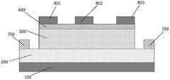
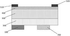
具体的,结合图1所示,本实施例中的肖特基二极管包括:沟道层300、势垒层400、背部盖帽层200、欧姆金属层510、肖特基金属层520、衬底层100以及背部栅极层700。Specifically, as shown in FIG. 1, the Schottky diode in this embodiment includes: a
在本实施例中,势垒层400设于沟道层300的正面,背部盖帽层200设于沟道层300的背面,欧姆金属层510设于势垒层400的第一侧,肖特基金属层520设于势垒层400的第二侧,衬底层100设于背部盖帽层200的背面,背部栅极层700设于背部盖帽层200的背面,背部栅极层700与衬底层100互不接触。In this embodiment, the
在本实施例中,欧姆金属层510与氮化镓基HEMT器件的漏极电极连接,肖特基金属层520与所述氮化镓基HEMT器件的源极电极连接,该肖特基二极管由沟道层300、势垒层400、背部盖帽层200以及背部栅极层700组成,背部栅极层700设于背部盖帽层200的背面,并与同样位于背部盖帽层200背面的衬底层100互不接触,通过对背部栅极层700的电压动态控制,实现较低的正向导通电阻以及较高的器件耐压,提高了器件在非嵌位感性负载开关过程测试中的性能,解决了相关技术中由于GaN基的HEMT缺乏相应的寄生二极管,导致其在UIS测试中产生的回灌电流在器件内部振荡,对器件造成毁灭性损伤的技术问题。In this embodiment, the
在一个实施例中,欧姆金属层510可以与势垒层400以及沟道层300之间形成欧姆接触,肖特基金属层520可以与势垒层400以及沟道层300之间形成肖特基接触。In one embodiment, the
在一个实施例中,结合图1所示,欧姆金属层510和肖特基金属层520呈L形结构。In one embodiment, as shown in FIG. 1 , the
在一个实施例中,结合图1所示,肖特基二极管还包括钝化层600,钝化层600设于欧姆金属层510的水平部与势垒层400之间,以及肖特基金属层520的水平部与势垒层400之间,欧姆金属层510的垂直部设于势垒层400的第一侧的表面,肖特基金属层520的垂直部设于势垒层400的第二侧的表面。In one embodiment, as shown in FIG. 1, the Schottky diode further includes a
在本实施例中,钝化层600设于欧姆金属层510的水平部与势垒层400之间,以及肖特基金属层520的水平部与势垒层400之间,欧姆金属层510的水平部和肖特基金属层520的水平部可以帮助减弱肖特基二极管的阳极或者阴极附近的电场尖峰。In this embodiment, the
在一个实施例中,欧姆金属层510的水平部的宽度大于欧姆金属层510的垂直部的宽度。In one embodiment, the width of the horizontal portion of the
在一个实施例中,肖特基金属层520的水平部的宽度大于肖特基金属层520的垂直部的宽度。In one embodiment, the width of the horizontal portion of the
在一个实施例中,势垒层400为AlGaN,沟道层300为氮化镓。In one embodiment, the
在本实施例中,沟道层300可以均由氮化镓材料制备。In this embodiment, the
在一个实施例中,可以通过在背部盖帽层200上沉积氮化镓材料或者外延生长氮化镓材料形成,其厚度大于背部盖帽层200的厚度。In one embodiment, it can be formed by depositing GaN material or epitaxially growing GaN material on the
在一个实施例中,背部盖帽层200为P型氮化镓。In one embodiment, the
在本实施例中,背部盖帽层200可以均由氮化镓材料中注入P型掺杂离子制备。In this embodiment, the
在一个实施例中,可以通过在衬底层100上沉积P型氮化镓材料或者外延生长P型氮化镓材料形成背部盖帽层200。In one embodiment, the
在一个实施例中,沟道层300的厚度大于势垒层400的厚度。In one embodiment, the thickness of the
在一个实施例中,肖特基二极管设于所述氮化镓基HEMT器件的栅极电极、漏极电极或者源极电极下方,且所述肖特基金属层与所述氮化镓基HEMT器件的源极电极连接,所述欧姆金属层与所述氮化镓基HEMT器件的漏极电极连接。In one embodiment, the Schottky diode is arranged under the gate electrode, the drain electrode or the source electrode of the GaN-based HEMT device, and the Schottky metal layer and the GaN-based HEMT The source electrode of the device is connected, and the ohmic metal layer is connected to the drain electrode of the GaN-based HEMT device.
在一个实施例中,结合图2所示,氮化镓基HEMT器件的源极金属层801、栅极金属层802以及漏极金属层803分别设于势垒层400上。In one embodiment, as shown in FIG. 2 , the
在本实施例中,氮化镓基HEMT器件的源极金属层801与其源极电极连接,氮化镓基HEMT器件的漏极金属层803与其漏极电极连接,氮化镓基HEMT器件的栅极金属层802与其栅极电极连接。In this embodiment, the
结合图2所示,背部栅极层700还设于氮化镓基HEMT器件的背部盖帽层700的两侧,本实施例中的氮化镓基HEMT器件的背部盖帽层700可以用于接入背部栅极电压,达到对器件内部的二维电子气通道进行调节,例如,若背部栅极电压大于0V,则二维电子气得到增强,可以降低正向导通的电阻,若背部栅极电压小于0V,则二维电子气被削弱,可以提高器件的反向偏置时的耐压。As shown in FIG. 2, the
在一个实施例中,背部栅极层700若设于欧姆金属层510和肖特基金属层520之间,则欧姆金属层510和肖特基金属层520以背部栅极层700所在的中轴线为轴对称设置。In one embodiment, if the
在一个实施例中,欧姆金属层510和肖特基金属层520下方的沟道层300、势垒层400、背部盖帽层200与氮化镓基HEMT器件的源极金属层801、栅极金属层802以及漏极金属层803下方的沟道层300、势垒层400、背部盖帽层200之间采用隔离材料层进行隔离。In one embodiment, the
在一个实施例中,该隔离材料层可以为氧化硅或者氮化硅,也可以为有机绝缘隔离材料。In one embodiment, the isolation material layer may be silicon oxide or silicon nitride, or an organic insulating isolation material.
本申请实施例还提供了一种氮化镓基HEMT器件的制备方法,参见图3所示,本实施例中的制备方法包括步骤S10至步骤S40。The embodiment of the present application also provides a method for manufacturing a gallium nitride-based HEMT device, as shown in FIG. 3 , the method for manufacturing in this embodiment includes steps S10 to S40.
在步骤S10中,在衬底层100的正面形成层叠设置的背部盖帽层200、沟道层300和势垒层400。In step S10 , a
在本实施例中,结合图4所示,背部盖帽层200、沟道层300和势垒层400层叠设于衬底层100的正面,背部盖帽层200设于沟道层300的背面,势垒层400设于沟道层300的正面。In this embodiment, as shown in FIG. 4 , the
在一个实施例中,势垒层400为AlGaN,沟道层300为氮化镓。In one embodiment, the
在一个实施例中,背部盖帽层200、沟道层300和势垒层400可以通过常规外延工艺在衬底100上形成。In one embodiment, the
在一个实施例中,背部盖帽层200为P型氮化镓。In one embodiment, the
在一个实施例中,沟道层300的厚度大于势垒层400的厚度。In one embodiment, the thickness of the
在步骤S20中,在势垒层400的第一侧形成欧姆金属层510,在势垒层400的第二侧形成肖特基金属层520。In step S20 , an
在本实施例中,结合图5所示,欧姆金属层510设于势垒层400的第一侧,肖特基金属层520设于势垒层400的第二侧。In this embodiment, as shown in FIG. 5 , the
在一个实施例中,欧姆金属层510可以与势垒层400以及沟道层300之间形成欧姆接触,肖特基金属层520可以与势垒层400以及沟道层300之间形成肖特基接触。In one embodiment, the
在一个实施例中,欧姆金属层510和肖特基金属层520可以呈L形结构,其结构如图1所示。In one embodiment, the
在一个实施例中,步骤S20之前还包括在势垒层400上形成钝化层600,钝化层600的位置如图1所示。In one embodiment, before step S20 , forming a
钝化层600设于欧姆金属层510的水平部与势垒层400之间,以及肖特基金属层520的水平部与势垒层400之间,欧姆金属层510的垂直部设于势垒层400的第一侧的表面,肖特基金属层520的垂直部设于势垒层400的第二侧的表面。The
在本实施例中,钝化层600设于欧姆金属层510的水平部与势垒层400之间,以及肖特基金属层520的水平部与势垒层400之间,欧姆金属层510的水平部和肖特基金属层520的水平部可以帮助减弱肖特基二极管的阳极或者阴极附近的电场尖峰。In this embodiment, the
在一个实施例中,欧姆金属层510的水平部的宽度大于欧姆金属层510的垂直部的宽度。In one embodiment, the width of the horizontal portion of the
在一个实施例中,肖特基金属层520的水平部的宽度大于肖特基金属层520的垂直部的宽度。In one embodiment, the width of the horizontal portion of the
在本实施例中,氮化镓基HEMT器件的源极金属层801与其源极电极连接,氮化镓基HEMT器件的漏极金属层803与其漏极电极连接,氮化镓基HEMT器件的栅极金属层802与其栅极电极连接。In this embodiment, the
在步骤S30中,对衬底层100的背面的指定区域进行刻蚀形成刻蚀区101。In step S30 , a designated area on the back surface of the
在本实施例中,结合图6所示,刻蚀区101深入至背部盖帽层200。In this embodiment, as shown in FIG. 6 , the
在一个实施例中,刻蚀区101至少覆盖与欧姆金属层510和肖特基金属层520之间的区域。In one embodiment, the
在步骤S40中,结合图7所示,在刻蚀区101形成与衬底层100互不接触的背部栅极层700。In step S40 , as shown in FIG. 7 , a
在本实施例中,背部栅极层700的位置与欧姆金属层510和肖特基金属层520的位置交错。In this embodiment, the position of the
在一个实施例中,背部栅极层700设于欧姆金属层510和肖特基金属层520之间,则欧姆金属层510和肖特基金属层520以背部栅极层700所在的中轴线为轴对称设置。In one embodiment, the
本申请实施例还提供了一种芯片,所述芯片包括如上述任一项所述的氮化镓基HEMT器件。The embodiment of the present application also provides a chip, the chip includes the GaN-based HEMT device according to any one of the above.
在一个实施例中,所述芯片包括如上述任一项所述的制备方法制备的氮化镓基HEMT器件。In one embodiment, the chip includes a gallium nitride-based HEMT device prepared by any one of the above-mentioned preparation methods.
在本实施例中,结合图2所示,肖特基二极管基于氮化镓基HEMT器件的沟道层300、势垒层400、背部盖帽层200制备,在实际应用中,背部栅极层700还设于氮化镓基HEMT器件的背部盖帽层700的两侧。In this embodiment, as shown in FIG. 2, the Schottky diode is prepared based on the
在一个实施例中,欧姆金属层510和肖特基金属层520下方的沟道层300、势垒层400、背部盖帽层200与氮化镓基HEMT器件的源极金属层801、栅极金属层802以及漏极金属层803下方的沟道层300、势垒层400、背部盖帽层200之间采用隔离材料层进行隔离。In one embodiment, the
本实施例中的氮化镓基HEMT器件的背部盖帽层700可以用于接入背部栅极电压,达到对器件内部的二维电子气通道进行调节,例如,若背部栅极电压大于0V,则二维电子气得到增强,可以降低正向导通的电阻,若背部栅极电压小于0V,则二维电子气被削弱,可以提高器件的反向偏置时的耐压。The
本申请实施例与现有技术相比存在的有益效果是:通过在氮化镓基HEMT器件内集成肖特基二极管,该肖特基二极管由沟道层、势垒层、背部盖帽层以及背部栅极层组成,背部栅极层设于背部盖帽层的背面,并与同样位于背部盖帽层背面的衬底层互不接触,通过对背部栅极层的电压动态控制,实现较低的正向导通电阻以及较高的器件耐压,提高了器件在非嵌位感性负载开关过程测试中的性能,解决了相关技术中由于GaN基的HEMT缺乏相应的寄生二极管,导致其在UIS测试中产生的回灌电流在器件内部振荡,对器件造成毁灭性损伤的技术问题。The beneficial effect of the embodiment of the present application compared with the prior art is: by integrating a Schottky diode in a gallium nitride-based HEMT device, the Schottky diode is composed of a channel layer, a barrier layer, a back capping layer and a back The back gate layer is set on the back of the back cap layer, and does not contact the substrate layer that is also located on the back of the back cap layer. By dynamically controlling the voltage of the back gate layer, a lower forward conduction is achieved. Resistance and high device withstand voltage improve the performance of the device in the test of the non-embedded inductive load switching process, and solve the problem in the UIS test caused by the lack of corresponding parasitic diodes in the GaN-based HEMT in the related technology The sinking current oscillates inside the device and causes destructive damage to the device.
所属领域的技术人员可以清楚地了解到,为了描述的方便和简洁,仅以上述各掺杂区区的划分进行举例说明,实际应用中,可以根据需要而将上述功能区分配由不同的掺杂区完成,即将所述装置的内部结构划分成不同的掺杂区,以完成以上描述的全部或者部分功能。Those skilled in the art can clearly understand that for the convenience and brevity of description, only the division of the above-mentioned doped regions is used as an example. In practical applications, the above-mentioned functional regions can be assigned to different doped regions according to needs. Completion means that the internal structure of the device is divided into different doped regions, so as to complete all or part of the functions described above.
实施例中的各掺杂区可以集成在一个功能区中,也可以是各个掺杂区单独物理存在,也可以两个或两个以上掺杂区集成在一个功能区中,上述集成的功能区既可以采用同种掺杂离子实现,也可以采用多种掺杂离子共同实现。另外,各掺杂区的具体名称也只是为了便于相互区分,并不用于限制本申请的保护范围。上述器件的制备方法中的中掺杂区的具体工作过程,可以参考前述方法实施例中的对应过程,在此不再赘述。Each doped region in the embodiment can be integrated in one functional region, or each doped region can exist separately physically, or two or more doped regions can be integrated in one functional region. The above-mentioned integrated functional region It can be realized by using the same kind of dopant ions, and can also be realized by using multiple dopant ions together. In addition, the specific names of the doped regions are only for the convenience of distinguishing each other, and are not used to limit the protection scope of the present application. For the specific working process of the medium-doped region in the above-mentioned device manufacturing method, reference may be made to the corresponding process in the foregoing method embodiments, and details will not be repeated here.
以上所述实施例仅用以说明本申请的技术方案,而非对其限制;尽管参照前述实施例对本申请进行了详细的说明,本领域的普通技术人员应当理解:其依然可以对前述各实施例所记载的技术方案进行修改,或者对其中部分技术特征进行等同替换;而这些修改或者替换,并不使相应技术方案的本质脱离本申请各实施例技术方案的精神和范围,均应包含在本申请的保护范围之内。The above-described embodiments are only used to illustrate the technical solutions of the present application, rather than to limit them; although the present application has been described in detail with reference to the foregoing embodiments, those of ordinary skill in the art should understand that: it can still implement the foregoing embodiments Modifications to the technical solutions described in the examples, or equivalent replacements for some of the technical features; and these modifications or replacements do not make the essence of the corresponding technical solutions deviate from the spirit and scope of the technical solutions of the various embodiments of the application, and should be included in the Within the protection scope of this application.
Claims (10)
Translated fromChinesePriority Applications (1)
| Application Number | Priority Date | Filing Date | Title |
|---|---|---|---|
| CN202211310772.6ACN115663017B (en) | 2022-10-25 | 2022-10-25 | Gallium nitride-based HEMT device, preparation method thereof and chip |
Applications Claiming Priority (1)
| Application Number | Priority Date | Filing Date | Title |
|---|---|---|---|
| CN202211310772.6ACN115663017B (en) | 2022-10-25 | 2022-10-25 | Gallium nitride-based HEMT device, preparation method thereof and chip |
Publications (2)
| Publication Number | Publication Date |
|---|---|
| CN115663017Atrue CN115663017A (en) | 2023-01-31 |
| CN115663017B CN115663017B (en) | 2025-08-01 |
Family
ID=84990523
Family Applications (1)
| Application Number | Title | Priority Date | Filing Date |
|---|---|---|---|
| CN202211310772.6AActiveCN115663017B (en) | 2022-10-25 | 2022-10-25 | Gallium nitride-based HEMT device, preparation method thereof and chip |
Country Status (1)
| Country | Link |
|---|---|
| CN (1) | CN115663017B (en) |
Cited By (1)
| Publication number | Priority date | Publication date | Assignee | Title |
|---|---|---|---|---|
| CN116314313A (en)* | 2023-02-24 | 2023-06-23 | 天狼芯半导体(成都)有限公司 | A cascode HEMT power device, its preparation method, and chip |
Citations (4)
| Publication number | Priority date | Publication date | Assignee | Title |
|---|---|---|---|---|
| US20100019279A1 (en)* | 2008-04-02 | 2010-01-28 | The Hong Kong University Of Science And Technology | Integrated HEMT and Lateral Field-Effect Rectifier Combinations, Methods, and Systems |
| CN102891171A (en)* | 2011-07-21 | 2013-01-23 | 联华电子股份有限公司 | Nitride semiconductor device and manufacturing method thereof |
| KR20140028424A (en)* | 2012-08-29 | 2014-03-10 | 엘지이노텍 주식회사 | Semiconductor device for high power |
| CN108807524A (en)* | 2017-09-06 | 2018-11-13 | 苏州捷芯威半导体有限公司 | Semiconductor devices and its manufacturing method |
- 2022
- 2022-10-25CNCN202211310772.6Apatent/CN115663017B/enactiveActive
Patent Citations (4)
| Publication number | Priority date | Publication date | Assignee | Title |
|---|---|---|---|---|
| US20100019279A1 (en)* | 2008-04-02 | 2010-01-28 | The Hong Kong University Of Science And Technology | Integrated HEMT and Lateral Field-Effect Rectifier Combinations, Methods, and Systems |
| CN102891171A (en)* | 2011-07-21 | 2013-01-23 | 联华电子股份有限公司 | Nitride semiconductor device and manufacturing method thereof |
| KR20140028424A (en)* | 2012-08-29 | 2014-03-10 | 엘지이노텍 주식회사 | Semiconductor device for high power |
| CN108807524A (en)* | 2017-09-06 | 2018-11-13 | 苏州捷芯威半导体有限公司 | Semiconductor devices and its manufacturing method |
Cited By (1)
| Publication number | Priority date | Publication date | Assignee | Title |
|---|---|---|---|---|
| CN116314313A (en)* | 2023-02-24 | 2023-06-23 | 天狼芯半导体(成都)有限公司 | A cascode HEMT power device, its preparation method, and chip |
Also Published As
| Publication number | Publication date |
|---|---|
| CN115663017B (en) | 2025-08-01 |
Similar Documents
| Publication | Publication Date | Title |
|---|---|---|
| US10593666B2 (en) | Method of forming a heterojunction semiconductor device having integrated clamping device | |
| US11322606B2 (en) | Heterojunction semiconductor device having high blocking capability | |
| EP2793255B1 (en) | Manufacturing method of a semiconductor device comprising a schottky diode and a high electron mobility transistor | |
| US9543291B2 (en) | Method of forming a high electron mobility semiconductor device and structure therefor | |
| KR101562879B1 (en) | Semiconductor device | |
| CN107359196B (en) | Semiconductor device with a plurality of semiconductor chips | |
| US8618557B2 (en) | Wide-band-gap reverse-blocking MOS-type semiconductor device | |
| US9087704B2 (en) | Semiconductor devices and methods of manufacturing the semiconductor device | |
| US20230036698A1 (en) | Reverse blocking gallium nitride high electron mobility transistor | |
| US10529708B2 (en) | Conductivity modulated drain extended MOSFET | |
| US20230387283A1 (en) | Enhancement-mode switching device and preparation method therefor | |
| CN108878524A (en) | A kind of GaN base transistor with high electronic transfer rate | |
| CN114530492A (en) | Lateral gallium nitride schottky diode structure with hybrid high-k dielectric field plate | |
| CN107958939A (en) | One kind nitridation Gallium base heterojunction Schottky diode structures | |
| CN111312815A (en) | GaN-based power transistor structure and preparation method thereof | |
| CN115663017A (en) | Gallium nitride based HEMT device, preparation method thereof and chip | |
| KR102241012B1 (en) | Diode embedded semiconductor device | |
| CN113871479A (en) | Transistor structure and preparation method thereof | |
| CN107958931A (en) | One kind nitridation Gallium base heterojunctions field-effect transistor structure of resistance to breakdown | |
| CN107958930A (en) | One kind nitridation Gallium radical heterojunction field effect transistor structures | |
| CN113871478A (en) | Novel semiconductor device with P-type channel based on double gate | |
| CN113497137A (en) | Semiconductor device and preparation method thereof | |
| CN205140988U (en) | Semiconductor device | |
| KR102137749B1 (en) | Power semiconductor device | |
| CN115602710A (en) | Gallium nitride-based diode device, preparation method and gallium nitride HEMT |
Legal Events
| Date | Code | Title | Description |
|---|---|---|---|
| PB01 | Publication | ||
| PB01 | Publication | ||
| SE01 | Entry into force of request for substantive examination | ||
| SE01 | Entry into force of request for substantive examination | ||
| GR01 | Patent grant | ||
| GR01 | Patent grant |