CN115655118A - Two-dimensional lattice grating in-plane displacement sensor with optical self-subdivision function - Google Patents
Two-dimensional lattice grating in-plane displacement sensor with optical self-subdivision functionDownload PDFInfo
- Publication number
- CN115655118A CN115655118ACN202211243661.8ACN202211243661ACN115655118ACN 115655118 ACN115655118 ACN 115655118ACN 202211243661 ACN202211243661 ACN 202211243661ACN 115655118 ACN115655118 ACN 115655118A
- Authority
- CN
- China
- Prior art keywords
- grating
- quadrant
- subdivision
- array
- layer
- Prior art date
- Legal status (The legal status is an assumption and is not a legal conclusion. Google has not performed a legal analysis and makes no representation as to the accuracy of the status listed.)
- Pending
Links
Images


Landscapes
- Length Measuring Devices By Optical Means (AREA)
Abstract
Description
Translated fromChinese技术领域technical field
本发明属于位移传感器技术领域,具体涉及一种具有光学自细分功能的二维点阵光栅面内位移传感器。The invention belongs to the technical field of displacement sensors, in particular to a two-dimensional lattice grating in-plane displacement sensor with optical self-subdivision function.
背景技术Background technique
超精密、高稳定性的二维位移测量在半导体制造、光刻、芯片加工制备等领域的发展过程中发挥着极其重要的作用。近年来,光刻和芯片制造技术快速发展,对位移测量精度、稳定性、行程等技术指标提出了更高的要求。目前,主流的位移检测原理包括:激光干涉式测量法以及利用光栅的单次一级衍射光干涉效应的光栅式位移测量。其中,光栅式位移传感器受益于其能进行绝对位置测量的优点,在光刻机、原子力显微镜等集成化精密加工测试设备与系统中得到广泛应用。传统光栅式位移检测的原理基于多路衍射光的干涉效应。此类器件采用空间光干涉技术,并且需要滤波片、分束器、反射镜等大量光学元件,使得系统复杂、体积较大、稳定性差。此外,该方法需要采用两个一维位移传感器组合的方式,实现二维位移测量。过程中由于存在系统装配误差,往往会对测量精度造成较大影响。基于光学自成像原理,采用双层光栅结构可以顺利实现面内二维位移测量,该方案可以有效简化光路结构、提高系统稳定性和集成度。然而,该方法相较于传统多级次衍射干涉式位移传感器而言,无法实现光学细分,因此在相同电子细分倍数情况下分辨率较差。Ultra-precise and high-stability two-dimensional displacement measurement plays an extremely important role in the development of semiconductor manufacturing, lithography, chip processing and preparation. In recent years, the rapid development of lithography and chip manufacturing technology has put forward higher requirements for technical indicators such as displacement measurement accuracy, stability, and stroke. At present, the mainstream displacement detection principles include: laser interferometry and grating displacement measurement using the single-order first-order diffracted light interference effect of the grating. Among them, the grating displacement sensor benefits from its advantages of absolute position measurement, and is widely used in integrated precision processing and testing equipment and systems such as lithography machines and atomic force microscopes. The principle of traditional grating displacement detection is based on the interference effect of multi-channel diffracted light. Such devices use spatial light interference technology and require a large number of optical components such as filters, beam splitters, and mirrors, making the system complex, large in size, and poor in stability. In addition, this method requires the combination of two one-dimensional displacement sensors to realize two-dimensional displacement measurement. Due to the existence of system assembly errors in the process, it often has a great impact on the measurement accuracy. Based on the principle of optical self-imaging, the in-plane two-dimensional displacement measurement can be successfully realized by using a double-layer grating structure. This solution can effectively simplify the optical path structure and improve system stability and integration. However, compared with the traditional multi-order diffraction interferometric displacement sensor, this method cannot achieve optical subdivision, so the resolution is poor under the same electronic subdivision multiple.
发明内容Contents of the invention
针对上述传统光栅式位移检测系统复杂、体积较大、稳定性差,且采用双层光栅结构无法实现光学细分的技术问题,本发明提供了一种结构简单、体积小、稳定性强、分辨率高的具有光学自细分功能的二维点阵光栅面内位移传感器。Aiming at the above-mentioned technical problems that the traditional grating type displacement detection system is complicated, large in size and poor in stability, and the optical subdivision cannot be realized by adopting a double-layer grating structure, the present invention provides a simple structure, small volume, strong stability, high resolution High two-dimensional dot matrix grating in-plane displacement sensor with optical self-subdivision function.
为了解决上述技术问题,本发明采用的技术方案为:In order to solve the problems of the technologies described above, the technical solution adopted in the present invention is:
一种具有光学自细分功能的二维点阵光栅面内位移传感器,包括激光器、准直扩束器、上层光栅、下层四象限阵列光栅、四象限探测器、细分电路模块,所述激光器的光路方向上设置有准直扩束器,所述准直扩束器的光路方向上设置有上层光栅,所述上层光栅的光路方向上设置有下层四象限阵列光栅,所述下层四象限阵列光栅的光路方向上设置有四象限探测器,所述四象限探测器与细分电路模块电性连接。A two-dimensional lattice grating in-plane displacement sensor with optical self-subdivision function, including a laser, a collimating beam expander, an upper layer grating, a lower four-quadrant array grating, a four-quadrant detector, and a subdivision circuit module, the laser A collimating beam expander is arranged on the optical path direction of the collimating beam expander, an upper grating is arranged on the optical path direction of the collimating beam expander, and a lower four-quadrant array grating is arranged on the optical path direction of the upper layer grating, and the lower four-quadrant array A four-quadrant detector is arranged in the optical path direction of the grating, and the four-quadrant detector is electrically connected with the subdivision circuit module.
所述上层光栅与待测位移物体贴合连接,所述下层四象限阵列光栅与四象限探测器贴合连接。The upper grating is bonded to the displacement object to be measured, and the lower four-quadrant array grating is bonded to the four-quadrant detector.
所述上层光栅采用二维蜂窝状六边形圆孔周期结构分布,所述上层光栅的每行或每列圆孔的圆心在同一平行线上,相邻所述平行线之间的距离为光栅周期长度,相邻所述平行线上的圆孔彼此相外切。The upper grating is distributed in a two-dimensional honeycomb hexagonal circular hole periodic structure, the centers of the circular holes in each row or column of the upper grating are on the same parallel line, and the distance between adjacent parallel lines is the grating Period length, circular holes on adjacent parallel lines are circumscribed to each other.
所述下层四象限阵列光栅采用四象限阵列圆孔二维平面光栅,所述下层四象限阵列光栅包括第一象限光栅、第二象限光栅、第三象限光栅和第四象限光栅,所述第一象限光栅与第二象限光栅并列设置,所述第三象限光栅与第四象限光栅并列设置。The lower four-quadrant array grating adopts a four-quadrant array circular hole two-dimensional planar grating, and the lower four-quadrant array grating includes a first quadrant grating, a second quadrant grating, a third quadrant grating and a fourth quadrant grating, and the first The quadrant grating is arranged in parallel with the second quadrant grating, and the third quadrant grating is arranged in parallel with the fourth quadrant grating.
所述第一象限光栅与第二象限光栅在横向距离上相隔n+1/4(n=0,1,2,3…)个光栅周期,所述第三象限光栅与第四象限光栅在纵向距离上相隔n+1/4(n=0,1,2,3…)个光栅周期。The first quadrant grating is separated from the second quadrant grating by n+1/4 (n=0, 1, 2, 3...) grating periods in the lateral distance, and the third quadrant grating is vertically separated from the fourth quadrant grating. There are n+1/4 (n=0, 1, 2, 3...) grating periods apart in distance.
所述激光器的激光波长为635nm,所述激光器的功率为1.2mw,所述细分电路模块的电路细分倍数为1000倍。The laser wavelength of the laser is 635nm, the power of the laser is 1.2mw, and the circuit subdivision multiple of the subdivision circuit module is 1000 times.
所述上层光栅和下层四象限阵列光栅的光栅圆孔直径为450nm,所述上层光栅和下层四象限阵列光栅的光栅占空比为0.5,所述上层光栅和下层四象限阵列光栅的光栅厚度为150nm,所述上层光栅和下层四象限阵列光栅的光栅材料为AI,所述上层光栅和下层四象限阵列光栅的光栅周期为900nm,所述上层光栅的光栅面积为10mm*10mm。The grating hole diameter of the upper layer grating and the lower four-quadrant array grating is 450nm, the grating duty ratio of the upper layer grating and the lower four-quadrant array grating is 0.5, and the grating thickness of the upper layer grating and the lower four-quadrant array grating is 150nm, the grating material of the upper grating and the lower four-quadrant array grating is AI, the grating period of the upper grating and the lower four-quadrant array grating is 900nm, and the grating area of the upper grating is 10mm*10mm.
所述第一象限光栅、第二象限光栅、第三象限光栅和第四象限光栅的光栅面积均为2.5mm*2.5mm。The grating areas of the first quadrant grating, the second quadrant grating, the third quadrant grating and the fourth quadrant grating are all 2.5mm*2.5mm.
所述下层四象限阵列光栅位于上层光栅的有效自成像距离D之内,所述下层四象限阵列光栅处于自成像半周期或周期位置Z处;The lower four-quadrant array grating is located within the effective self-imaging distance D of the upper grating, and the lower four-quadrant array grating is at self-imaging half-period or periodic position Z;


所述d为上层光栅与下层四象限阵列光栅的光栅周期,所述N为光栅周期的个数,所述n为单个周期光栅的衍射级次,所述N、n均为整数0、1、2…。The d is the grating period of the upper grating and the lower four-quadrant array grating, the N is the number of the grating period, and the n is the diffraction order of a single period grating, and the N and n are
一种具有光学自细分功能的二维点阵光栅面内位移传感器测量方法,包括下列步骤:A method for measuring a two-dimensional lattice grating in-plane displacement sensor with an optical self-subdivision function, comprising the following steps:
S1、激光器发出的光经准直扩束器准直扩束后,沿直线传播并径直入射到上层光栅上;S1. After the light emitted by the laser is collimated and expanded by the collimating beam expander, it propagates along a straight line and is directly incident on the upper grating;
S2、上层光栅与待测位移物体贴合在一起,随待测位移物体一起在平面内进行移动;S2. The upper grating is attached to the displacement object to be measured, and moves in the plane together with the displacement object to be measured;
S3、光束径直穿过下层四象限阵列光栅,下层四象限阵列光栅与四象限探测器紧紧贴合在一起;S3. The light beam passes directly through the lower four-quadrant array grating, and the lower four-quadrant array grating is closely attached to the four-quadrant detector;
S4、由四象限探测器将上层光栅、下层四象限阵列光栅在二维平面产生面内相对移动时整个系统光强透射率信号进行采集,得到两组共四路正弦信号;S4. The four-quadrant detector collects the light intensity transmittance signal of the entire system when the upper layer grating and the lower four-quadrant array grating move relatively in the two-dimensional plane, and obtains two sets of four-way sinusoidal signals;
S5、每组信号由两路相位彼此相差90°的正余弦信号组成,分别用于X方向和Y方向位移的检测,定义横向方向为X方向,定义纵向方向为Y方向,第一象限光栅与第二象限光栅产生X方向的信号,第三象限光栅与第四象限光栅产生Y方向的信号;S5. Each group of signals is composed of two sine and cosine signals with a phase difference of 90° from each other, which are respectively used for the detection of displacement in the X direction and the Y direction. The horizontal direction is defined as the X direction, and the longitudinal direction is defined as the Y direction. The first quadrant grating and The second quadrant grating generates signals in the X direction, and the third quadrant grating and the fourth quadrant grating generate signals in the Y direction;
S6、两组信号通过细分电路模块对信号进行细分调制,对待测位移物体的面内位移进行测量。S6. The two groups of signals are subdivided and modulated by the subdivision circuit module, and the in-plane displacement of the displacement object to be measured is measured.
本发明与现有技术相比,具有的有益效果是:Compared with the prior art, the present invention has the beneficial effects of:
本发明基于双层二维圆孔阵列光栅结构光学自成像原理,实现了面内位移高分辨检测功能。基于光学自成像细分成像效应,实现了变化周期为光栅周期的二分之一的光学细分,即实现了两倍的光学细分,解决了传统双层光栅位移传感器无法实现光学细分的难题,提高了位移分辨率;并且本发明光路简单,无需反射镜、棱镜、滤光片、分束器等光学元件,光路简单,系统稳定,抗干扰能力强,利于微型化、集成化、高分辨位移检测应用。The invention is based on the optical self-imaging principle of the double-layer two-dimensional circular hole array grating structure, and realizes the high-resolution detection function of in-plane displacement. Based on the optical self-imaging subdivision imaging effect, the optical subdivision with a change period of half the grating period is realized, that is, twice the optical subdivision is realized, which solves the problem that the traditional double-layer grating displacement sensor cannot achieve optical subdivision difficult problem, and the displacement resolution is improved; and the optical path of the present invention is simple, without optical components such as mirrors, prisms, optical filters, beam splitters, etc., the optical path is simple, the system is stable, and the anti-interference ability is strong, which is beneficial to miniaturization, integration, high Resolution displacement detection applications.
附图说明Description of drawings
为了更清楚地说明本发明的实施方式或现有技术中的技术方案,下面将对实施方式或现有技术描述中所需要使用的附图作简单地介绍。显而易见地,下面描述中的附图仅仅是示例性的,对于本领域普通技术人员来讲,在不付出创造性劳动的前提下,还可以根据提供的附图引申获得其它的实施附图。In order to more clearly illustrate the embodiments of the present invention or the technical solutions in the prior art, the following will briefly introduce the accompanying drawings that are required in the description of the embodiments or the prior art. Apparently, the drawings in the following description are only exemplary, and those skilled in the art can obtain other implementation drawings according to the provided drawings without creative effort.
本说明书所绘示的结构、比例、大小等,均仅用以配合说明书所揭示的内容,以供熟悉此技术的人士了解与阅读,并非用以限定本发明可实施的限定条件,故不具技术上的实质意义,任何结构的修饰、比例关系的改变或大小的调整,在不影响本发明所能产生的功效及所能达成的目的下,均应仍落在本发明所揭示的技术内容能涵盖的范围内。The structures, proportions, sizes, etc. shown in this manual are only used to cooperate with the content disclosed in the manual, so that people familiar with this technology can understand and read, and are not used to limit the conditions for the implementation of the present invention, so there is no technical In the substantive meaning above, any modification of structure, change of proportional relationship or adjustment of size should still fall within the scope of the technical contents disclosed in the present invention without affecting the effects and goals that can be achieved by the present invention. within the scope covered.
图1为本发明的整体结构示意图;Fig. 1 is the overall structure schematic diagram of the present invention;
图2为本发明上层光栅的结构示意图;Fig. 2 is the structural representation of upper layer grating of the present invention;
图3为本发明上层光栅的二维面内仿真结果图;Fig. 3 is the two-dimensional in-plane simulation result figure of upper layer grating of the present invention;
图4为本发明上层光栅沿Z方向离面仿真结果图;Fig. 4 is the simulation result figure of the upper layer grating of the present invention along the Z direction;
图5为本发明下层四象限阵列光栅的结构示意图;Fig. 5 is the structural representation of the four-quadrant array grating of the lower layer of the present invention;
图6为本发明四象限探测器输出四个象限面内位移信号图;Fig. 6 is a diagram of displacement signals in four quadrant planes output by the four-quadrant detector of the present invention;
图7为本发明上层光栅沿X方向向移动两个光栅周期距离时单个象限透射光强FDTD随位移仿真结果图。Fig. 7 is a simulation result diagram of the FDTD of the transmitted light intensity of a single quadrant with displacement when the upper grating of the present invention is moved along the X direction for two grating period distances.
其中:1为激光器,2为准直扩束器,3为上层光栅,4为下层四象限阵列光栅,401为第一象限光栅,402为第二象限光栅,403为第三象限光栅,404为第四象限光栅,5为四象限探测器,6为细分电路模块。Among them: 1 is the laser, 2 is the collimator beam expander, 3 is the upper grating, 4 is the lower four-quadrant array grating, 401 is the first quadrant grating, 402 is the second quadrant grating, 403 is the third quadrant grating, 404 is The fourth quadrant grating, 5 is a four-quadrant detector, and 6 is a subdivision circuit module.
具体实施方式Detailed ways
为使本发明实施例的目的、技术方案和优点更加清楚,下面将对本发明实施例中的技术方案进行清楚、完整地描述,显然,所描述的实施例仅仅是本申请一部分实施例,而不是全部的实施例,这些描述只是为进一步说明本发明的特征和优点,而不是对本发明权利要求的限制;基于本申请中的实施例,本领域普通技术人员在没有做出创造性劳动前提下所获得的所有其他实施例,都属于本申请保护的范围。In order to make the purpose, technical solutions and advantages of the embodiments of the present invention clearer, the technical solutions in the embodiments of the present invention will be clearly and completely described below. Obviously, the described embodiments are only part of the embodiments of the application, rather than All the embodiments, these descriptions are only to further illustrate the features and advantages of the present invention, rather than to limit the claims of the present invention; based on the embodiments in the application, those of ordinary skill in the art can obtain without making creative work All other embodiments of all belong to the protection scope of this application.
下面结合附图和实施例,对本发明的具体实施方式做进一步详细描述。以下实施例用于说明本发明,但不用来限制本发明的范围。The specific implementation manners of the present invention will be further described in detail below in conjunction with the accompanying drawings and embodiments. The following examples are used to illustrate the present invention, but are not intended to limit the scope of the present invention.
术语“第一”、“第二”仅用于描述目的,而不能理解为指示或暗示相对重要性或者隐含指明所指示的技术特征的数量。由此,限定有“第一”、“第二”的特征可以明示或者隐含地包括一个或者更多个该特征。在本申请的描述中,除非另有说明,“多个”的含义是两个或两个以上。The terms "first" and "second" are used for descriptive purposes only, and cannot be understood as indicating or implying relative importance or implicitly specifying the quantity of indicated technical features. Thus, a feature defined as "first" and "second" may explicitly or implicitly include one or more of these features. In the description of the present application, unless otherwise specified, "plurality" means two or more.
在本申请的描述中,需要说明的是,除非另有明确的规定和限定,术语“安装”、“相连”、“连接”应做广义理解,例如,可以是固定连接,也可以是可拆卸连接,或一体的连接;可以是机械连接,也可以是电连接;可以是直接相连,也可以通过中间媒介间接相连,可以是两个元件内部的连通。对于本领域的普通技术人员而言,可以具体情况理解上述术语在本申请中的具体含义。In the description of this application, it should be noted that unless otherwise specified and limited, the terms "installation", "connection", and "connection" should be understood in a broad sense, for example, it can be a fixed connection or a detachable connection. Connection, or integral connection; it can be mechanical connection or electrical connection; it can be direct connection or indirect connection through an intermediary, and it can be the internal communication of two components. Those of ordinary skill in the art can understand the specific meanings of the above terms in this application in specific situations.
本实施例的具体参数为:激光器1的激光波长为635nm,激光器1的功率为1.2mw,细分电路模块6的电路细分倍数为1000倍。上层光栅3和下层四象限阵列光栅4的光栅圆孔直径为450nm,上层光栅3和下层四象限阵列光栅4的光栅占空比为0.5,上层光栅3和下层四象限阵列光栅4的光栅厚度为150nm,上层光栅3和下层四象限阵列光栅4的光栅材料为AI,上层光栅3和下层四象限阵列光栅4的光栅周期为900nm,上层光栅3的光栅面积为10mm*10mm。第一象限光栅401、第二象限光栅402、第三象限光栅403和第四象限光栅404的光栅面积均为2.5mm*2.5mm。The specific parameters of this embodiment are: the laser wavelength of the
在本实施例中,如图1所示,激光器1发出的光经准直扩束器2准直扩束后,沿直线传播并径直入射到上层光栅3上,其中,如图2所示,上层光栅3采用二维蜂窝状六边形圆孔周期结构分布,上层二维蜂窝状六边形圆孔周期结构光栅3的每行、列圆孔圆心在同一平行线上,且相邻平行线之间的距离为光栅周期长度,基本周期单元为六边形蜂窝状结构。并随位移待测物体在二维平面内移动。随后,光束径直穿过下层四象限阵列光栅4,其中,下层光栅4为四象限阵列圆孔二维平面光栅,由互相相隔n+1/4(n=0,1,2,3…)倍光栅周期的四个二维线性圆孔阵列组成,基本周期单元为矩形结构。然后,随着待测位移物体沿面内X或Y方向移动,系统整体透射细分光强信号由四象限探测器5收集,输出的光栅二维面内位移四个象限的信号图如图6所示,其中,象限1、2检测的为X轴向位移的两路相位彼此相差90°的正余弦信号;象限3、4检测的为Y轴向位移的两路相位彼此相差90°的正余弦信号。最终,得到的两组两路彼此相差90°的正余弦信号由后续的电路细分模块6进行电路细分处理得到具有一定分辨率的位移检测值。图7所示,为沿X轴向进行面内位移时的扫描仿真结果图,扫描位移长度为两个光栅周期的长度,得到的透射光强度实现了变化周期为光栅周期的二分之一(即实现了两倍的光学细分)的光强信号细分。In this embodiment, as shown in Figure 1, the light emitted by the
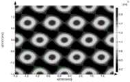
进一步,上层光栅3的二维面内仿真结果图,如图3所示,其仿真图形范围在FDTD内呈现为中心对称的二维阵列模块。从仿真结果图可以看出:仿真得到良好的蜂窝状六边形圆孔周期结构光栅面内自成像。Further, the two-dimensional in-plane simulation result diagram of the
进一步,上层光栅3沿X轴向离面仿真结果图,如图4所示,其仿真结果在FDTD中采用2D的xz面探测器进行探测。从仿真结果图中可以得出:上层二维蜂窝状六边形圆孔周期结构光栅3在离面方向上的泰伯自成像范围内,圆孔光斑分布图案呈现为错落有致的倒三角形。Further, the out-of-plane simulation result diagram of the
进一步,如图5所示,第一象限光栅401与第二象限光栅402在横向距离上相隔n+1/4(n=0,1,2,3…)个光栅周期,第三象限光栅403与第四象限光栅404在纵向距离上相隔n+1/4(n=0,1,2,3…)个光栅周期。Further, as shown in Figure 5, the first quadrant grating 401 and the second quadrant grating 402 are separated by n+1/4 (n=0,1,2,3...) grating periods in the lateral distance, and the third quadrant grating 403 It is separated from the fourth quadrant grating 404 by n+1/4 (n=0, 1, 2, 3 . . . ) grating periods in the longitudinal distance.
基于上层光栅的光学自成像效应,因此,为了保障良好的信号输出,下层四象限阵列光栅4位于上层光栅3的有效自成像距离D之内,同时下层四象限阵列光栅4需要处于自成像半周期或周期位置Z处。Based on the optical self-imaging effect of the upper grating, therefore, in order to ensure a good signal output, the lower four-quadrant array grating 4 is located within the effective self-imaging distance D of the


其中:d为上层光栅3与下层四象限阵列光栅4的光栅周期,N为光栅周期的个数,n为单个周期光栅的衍射级次,N、n均为整数0、1、2…。Where: d is the grating period of the
其中,本实施例利用光栅衍射现象中的自成像效应,采用具有光学自细分功能的二维点阵光栅面内位移测量系统对待测位移物体的面内位移进行测量,实现变化周期为光栅周期的二分之一(即实现了两倍的光学细分)的高分辨率光学信号细分,是本发明二维位移测量的核心,系统位移测量的分辨率Sin可以表示为:Among them, this embodiment uses the self-imaging effect in the grating diffraction phenomenon, and uses a two-dimensional lattice grating in-plane displacement measurement system with optical self-subdivision function to measure the in-plane displacement of the object to be measured, so that the change period is the grating period The high-resolution optical signal subdivision of 1/2 (promptly realizing twice the optical subdivision) is the core of the two-dimensional displacement measurement of the present invention, and the resolution Sin of the system displacement measurement can be expressed as:

式中S1为光学分辨率,由光学信号周期L决定;S2为电学分辨率,由细分电路细分倍数M决定。由该式可知,采用变化周期为光栅周期的二分之一(即实现了两倍的光学细分)的高分辨率光学细分周期信号,结合后续的电子细分,最终可在简单的电子细分条件下实现整个系统更高分辨率的位移检测。In the formula, S1 is the optical resolution, which is determined by the optical signal period L; S2 is the electrical resolution, which is determined by the subdivision multiple M of the subdivision circuit. It can be seen from this formula that the high-resolution optical subdivision periodic signal whose change period is half of the grating period (i.e. realize twice the optical subdivision), combined with the subsequent electronic subdivision, can finally be obtained in simple electronic subdivision. Realize higher resolution displacement detection of the whole system under subdivision conditions.
以本实施例中所给的参数为例:由图7可见,当上层光栅3和下层四象限阵列光栅4周期均采用900nm时,输出信号周期为450nm,即光学灵敏度为450nm,实现了变化周期为光栅周期的二分之一(即实现了两倍的光学细分)光学自细分。由式(3)可知当光学信号分辨率S1变为自成像周期分辨率的2倍时,测量系统整体分辨率Sin变为原来的2倍。当电路细分倍数为1000倍时,系统整体分辨率由0.9nm提升至0.45nm。Take the parameters given in this embodiment as an example: As can be seen from Figure 7, when the period of the
上面仅对本发明的较佳实施例作了详细说明,但是本发明并不限于上述实施例,在本领域普通技术人员所具备的知识范围内,还可以在不脱离本发明宗旨的前提下作出各种变化,各种变化均应包含在本发明的保护范围之内。Only the preferred embodiments of the present invention have been described in detail above, but the present invention is not limited to the above-mentioned embodiments. Within the scope of knowledge possessed by those of ordinary skill in the art, various modifications can also be made without departing from the gist of the present invention. Various changes should be included within the protection scope of the present invention.
Claims (10)


Priority Applications (1)
| Application Number | Priority Date | Filing Date | Title |
|---|---|---|---|
| CN202211243661.8ACN115655118A (en) | 2022-10-11 | 2022-10-11 | Two-dimensional lattice grating in-plane displacement sensor with optical self-subdivision function |
Applications Claiming Priority (1)
| Application Number | Priority Date | Filing Date | Title |
|---|---|---|---|
| CN202211243661.8ACN115655118A (en) | 2022-10-11 | 2022-10-11 | Two-dimensional lattice grating in-plane displacement sensor with optical self-subdivision function |
Publications (1)
| Publication Number | Publication Date |
|---|---|
| CN115655118Atrue CN115655118A (en) | 2023-01-31 |
Family
ID=84988302
Family Applications (1)
| Application Number | Title | Priority Date | Filing Date |
|---|---|---|---|
| CN202211243661.8APendingCN115655118A (en) | 2022-10-11 | 2022-10-11 | Two-dimensional lattice grating in-plane displacement sensor with optical self-subdivision function |
Country Status (1)
| Country | Link |
|---|---|
| CN (1) | CN115655118A (en) |
Citations (8)
| Publication number | Priority date | Publication date | Assignee | Title |
|---|---|---|---|---|
| US4757207A (en)* | 1987-03-03 | 1988-07-12 | International Business Machines Corporation | Measurement of registration of overlaid test patterns by the use of reflected light |
| JPH03115906A (en)* | 1989-09-29 | 1991-05-16 | Toshiba Corp | Method and device for position shift detection |
| US5666196A (en)* | 1993-05-31 | 1997-09-09 | Canon Kabushiki Kaisha | Optical detection apparatus for detecting information relating to relative displacement of an object on whch a diffraction grating is formed |
| JP2000205819A (en)* | 1999-01-13 | 2000-07-28 | Olympus Optical Co Ltd | Optical displacement sensor |
| CN106524921A (en)* | 2016-11-05 | 2017-03-22 | 中北大学 | High-accuracy wide-range double-layer nano-grating micro displacement detection device |
| CN110940830A (en)* | 2019-12-12 | 2020-03-31 | 中北大学 | Two-axis accelerometer structure based on two-dimensional grating and four-quadrant detector |
| CN113819847A (en)* | 2021-09-23 | 2021-12-21 | 中北大学 | Dislocation two-dimensional grating array-based double-grating structure three-dimensional micro-displacement sensor |
| CN114877809A (en)* | 2022-05-27 | 2022-08-09 | 中北大学 | A Displacement Measurement System Based on Two-dimensional Composite Planar Large-Range Grating Structure |
- 2022
- 2022-10-11CNCN202211243661.8Apatent/CN115655118A/enactivePending
Patent Citations (8)
| Publication number | Priority date | Publication date | Assignee | Title |
|---|---|---|---|---|
| US4757207A (en)* | 1987-03-03 | 1988-07-12 | International Business Machines Corporation | Measurement of registration of overlaid test patterns by the use of reflected light |
| JPH03115906A (en)* | 1989-09-29 | 1991-05-16 | Toshiba Corp | Method and device for position shift detection |
| US5666196A (en)* | 1993-05-31 | 1997-09-09 | Canon Kabushiki Kaisha | Optical detection apparatus for detecting information relating to relative displacement of an object on whch a diffraction grating is formed |
| JP2000205819A (en)* | 1999-01-13 | 2000-07-28 | Olympus Optical Co Ltd | Optical displacement sensor |
| CN106524921A (en)* | 2016-11-05 | 2017-03-22 | 中北大学 | High-accuracy wide-range double-layer nano-grating micro displacement detection device |
| CN110940830A (en)* | 2019-12-12 | 2020-03-31 | 中北大学 | Two-axis accelerometer structure based on two-dimensional grating and four-quadrant detector |
| CN113819847A (en)* | 2021-09-23 | 2021-12-21 | 中北大学 | Dislocation two-dimensional grating array-based double-grating structure three-dimensional micro-displacement sensor |
| CN114877809A (en)* | 2022-05-27 | 2022-08-09 | 中北大学 | A Displacement Measurement System Based on Two-dimensional Composite Planar Large-Range Grating Structure |
Non-Patent Citations (1)
| Title |
|---|
| 辛晨光等: "双光栅结构光学自成像效应位移检测应用研究", 《光学技术》, vol. 47, no. 6, 30 November 2021 (2021-11-30), pages 689 - 694* |
Similar Documents
| Publication | Publication Date | Title |
|---|---|---|
| US11525673B2 (en) | Five-degree-of-freedom heterodyne grating interferometry system | |
| CN103604375B (en) | Double frequency laser grating interference two-dimensional measurement method and system with optical aliasing resistance | |
| CN106017308B (en) | A kind of six degree of freedom interferometer measuration system and method | |
| CN101169601B (en) | Focusing leveling measuring system | |
| CN105737765A (en) | Four-freedom degree optical measuring head based on semiconductor laser assembly | |
| CN110285761B (en) | A compact grating three-dimensional displacement measuring device | |
| CN101846506B (en) | Roll angle measurement method based on common path parallel beams | |
| CN106813578B (en) | A kind of two-dimensional grating measuring system | |
| CN209894118U (en) | Displacement measurement system based on reflective single holographic grating | |
| CN110631483B (en) | Orthogonal grating three-degree-of-freedom magnetic levitation measurement sensor, detector and detection method thereof | |
| CN104567696A (en) | Two-dimensional displacement measuring device based on diffraction grating | |
| CN103673891A (en) | Grating heterodyne interference auto-collimation measuring device | |
| CN104567695A (en) | Three-dimensional displacement measurement device adopting double frequency laser and a diffraction grating | |
| CN106949842B (en) | Two-dimensional displacement measuring device and measuring method | |
| CN104596424A (en) | Two dimension displacement measurement device which uses double frequency laser and diffraction grating | |
| CN103217104A (en) | Non-guide measurement device and method of point diffraction three-dimensional absolute displacement | |
| CN109029272A (en) | A kind of dual-channel grating displacement measurement method | |
| CN115574722A (en) | Self-tracing interference type displacement sensor | |
| CN206618387U (en) | A kind of interferometric measuring means for diffraction grating displacement measurement system | |
| CN114111587A (en) | Three-axis high-optical subdivision grating ruler | |
| CN102865835A (en) | Vernier slit type photoelectric autocollimator | |
| CN115655118A (en) | Two-dimensional lattice grating in-plane displacement sensor with optical self-subdivision function | |
| CN114877809B (en) | Displacement measurement system based on two-dimensional composite plane wide-range grating structure | |
| CN110849293B (en) | A four-beam structure laser heterodyne interference roll angle measurement device and method | |
| CN204807051U (en) | Satellite outer corner measurement appearance based on two dimension PSD |
Legal Events
| Date | Code | Title | Description |
|---|---|---|---|
| PB01 | Publication | ||
| PB01 | Publication | ||
| SE01 | Entry into force of request for substantive examination | ||
| SE01 | Entry into force of request for substantive examination |