CN115647618A - Method for processing micropores on monocrystal yttrium iron garnet ferrite thick film composite substrate - Google Patents
Method for processing micropores on monocrystal yttrium iron garnet ferrite thick film composite substrateDownload PDFInfo
- Publication number
- CN115647618A CN115647618ACN202211375565.9ACN202211375565ACN115647618ACN 115647618 ACN115647618 ACN 115647618ACN 202211375565 ACN202211375565 ACN 202211375565ACN 115647618 ACN115647618 ACN 115647618A
- Authority
- CN
- China
- Prior art keywords
- composite substrate
- iron garnet
- hole
- thick film
- yttrium iron
- Prior art date
- Legal status (The legal status is an assumption and is not a legal conclusion. Google has not performed a legal analysis and makes no representation as to the accuracy of the status listed.)
- Pending
Links
Images

Landscapes
- Crystals, And After-Treatments Of Crystals (AREA)
Abstract
Description
Translated fromChinese技术领域technical field
本发明涉及激光加工技术,尤其是复合陶瓷基板的激光加工方法,具体是利用皮秒激光在单晶钇铁石榴石铁氧体厚膜复合基板上快速、高效地加工微孔的方法。The invention relates to a laser processing technology, especially a laser processing method for a composite ceramic substrate, in particular a method for rapidly and efficiently processing micropores on a single crystal yttrium iron garnet ferrite thick-film composite substrate by using a picosecond laser.
背景技术Background technique
单晶钇铁石榴石铁氧体(YIG)是一种具有良好的旋磁效应,低铁磁共振线宽,高电阻率,低介电损耗等特点微波铁氧体,已经被广泛应用于微波铁氧体器件中,如YIG调谐滤波器、振荡器等。为满足相控阵雷达对T/R组件小尺寸、低功耗、高集成度等性能的要求,开展单晶YIG单晶厚膜器件研究对于相控阵雷达的发展具有重要意义。近年来,国内在高性能的YIG单晶厚膜制备,微波铁氧体器件设计方面已取得不错成绩,但在YIG厚膜加工工艺方面(如刻蚀、通孔)与国外存在明显差异,使得小型化微波铁氧体器件发展缓慢,严重限制了我国在高性能有源相控阵雷达领域的发展。Single crystal yttrium iron garnet ferrite (YIG) is a microwave ferrite with good gyromagnetic effect, low ferromagnetic resonance linewidth, high resistivity, low dielectric loss, etc. It has been widely used in microwave Ferrite devices, such as YIG tuned filters, oscillators, etc. In order to meet the performance requirements of phased array radar for T/R components such as small size, low power consumption, and high integration, it is of great significance to carry out research on single crystal YIG single crystal thick film devices for the development of phased array radar. In recent years, China has made good achievements in the preparation of high-performance YIG single crystal thick film and the design of microwave ferrite devices, but there are obvious differences in YIG thick film processing technology (such as etching, through hole) and foreign countries, making The slow development of miniaturized microwave ferrite devices severely limits the development of high-performance active phased array radar in my country.
在YIG单晶膜的制备手段方面,国内已经发展出包括液相外延、激光分子束外延(PLD)等材料制备技术,能够在钆镓石榴石(GGG)衬底上制备出厚度从几十纳米至几十微米的高质量YIG单晶薄膜,可以被用在隔离器、滤波器、谐振器等微波器件中。单晶YIG铁氧体厚膜作为电磁功能基底使用时,如果只做平面型器件,会较大限制很多功能的实现,为解决立体器件,层间或者面间电路导通,则需要对单晶YIG铁氧体厚膜进行刻蚀或基片通孔。单晶YIG铁氧体厚膜存在较大的残余应力,在这种情况下进行直接刻蚀或通孔,难度很大。另外,文献调研表明目前尚未发现针对50微米厚度单晶YIG厚膜的成熟刻蚀和通孔技术。在这种强烈需求下,需要重点突破单晶YIG铁氧体厚膜刻蚀、通孔的关键技术。In terms of the preparation methods of YIG single crystal film, material preparation technologies including liquid phase epitaxy and laser molecular beam epitaxy (PLD) have been developed in China, which can prepare the thickness from tens of nanometers on the gadolinium gallium garnet (GGG) substrate. High-quality YIG single crystal thin films down to tens of microns can be used in microwave devices such as isolators, filters, and resonators. When a single crystal YIG ferrite thick film is used as an electromagnetic function substrate, if only planar devices are used, the realization of many functions will be greatly restricted. YIG ferrite thick film for etching or substrate through hole. The single crystal YIG ferrite thick film has a large residual stress, and it is very difficult to perform direct etching or through holes in this case. In addition, the literature survey shows that no mature etching and via technology for single crystal YIG thick film with a thickness of 50 microns has been found yet. Under this strong demand, it is necessary to focus on breakthroughs in the key technologies of single crystal YIG ferrite thick film etching and through holes.
发明内容Contents of the invention
本发明的目的是提供一种快速、高效地在单晶YIG铁氧体厚膜基板上加工微孔的方法,以解决目前YIG厚膜加工工艺及YIG单晶厚膜器件应用方面的问题。The purpose of the present invention is to provide a fast and efficient method for processing micro-holes on a single crystal YIG ferrite thick film substrate, so as to solve the problems in the current YIG thick film processing technology and the application of YIG single crystal thick film devices.
本发明的一个目的是解决至少上述问题和/或缺陷,并提供至少后面将说明的优点。An object of the present invention is to solve at least the above problems and/or disadvantages and to provide at least the advantages as will be described hereinafter.
为了实现根据本发明的这些目的和其它优点,提供了一种单晶钇铁石榴石铁氧体厚膜复合基板上的微孔加工方法,包括以下步骤;In order to achieve these objects and other advantages according to the present invention, a microhole processing method on a single crystal yttrium iron garnet ferrite thick film composite substrate is provided, comprising the following steps;
步骤一、单晶钇铁石榴石铁氧体厚膜复合基板的前处理:将单晶钇铁石榴石铁氧体厚膜复合基板表面打磨抛光、超声清洗和干燥;Step 1. Pretreatment of the single crystal yttrium iron garnet thick film composite substrate: polishing the surface of the single crystal yttrium iron garnet thick film composite substrate, ultrasonic cleaning and drying;
步骤二、加工圆形通孔:通过皮秒激光对前处理后的单晶钇铁石榴石铁氧体厚膜复合基板进行微加工,得到成形的圆形通孔;Step 2. Processing circular through-holes: micromachining the pre-treated single crystal yttrium-iron-garnet thick-film ferrite composite substrate with a picosecond laser to obtain formed circular through-holes;
步骤三、对加工圆形通孔后的单晶钇铁石榴石铁氧体厚膜复合基板进行后处理:将单晶钇铁石榴石铁氧体厚膜复合基板进行超声清洗,干燥后完成圆形通孔的微加工。Step 3: post-processing the single crystal yttrium iron garnet ferrite thick film composite substrate after the circular through hole is processed: ultrasonically clean the single crystal yttrium iron garnet ferrite thick film composite substrate, and complete the round after drying. Micromachining of shaped through-holes.
优选的是,所述步骤一中,单晶钇铁石榴石铁氧体厚膜复合基板由钆镓石榴石基底层和钇铁石榴石生长层构成,其结构为钇铁石榴石生长层/钆镓石榴石基底层/钇铁石榴石生长层,钆镓石榴石基底层厚度200~500微米,上层的钇铁石榴石生长层和下层的钇铁石榴石生长层的厚度均为30~60微米。Preferably, in the first step, the single crystal yttrium-iron-garnet thick-film ferrite composite substrate is composed of a base layer of gadolinium-gallium garnet and a growth layer of yttrium-iron garnet, and its structure is a growth layer of yttrium-iron garnet/gadolinium Gallium garnet base layer/yttrium iron garnet growth layer, the thickness of the gadolinium gallium garnet base layer is 200-500 microns, the thickness of the upper yttrium iron garnet growth layer and the lower yttrium iron garnet growth layer are both 30-60 microns .
优选的是,所述步骤一中,超声清洗采用在无水乙醇中进行。Preferably, in the first step, ultrasonic cleaning is performed in absolute ethanol.
优选的是,所述步骤二中,采用全固态激光器输出皮秒激光;所述皮秒激光的波长为1064nm,脉冲宽度10~15ps,平均输出功率10~20W,重复频率100~600kHz,扫描速度100~1000mm/s。Preferably, in the second step, an all-solid-state laser is used to output picosecond laser; the wavelength of the picosecond laser is 1064nm, the pulse width is 10-15ps, the average output power is 10-20W, the repetition frequency is 100-600kHz, and the scanning speed is 100~1000mm/s.
优选的是,所述步骤二中,加工圆形通孔的具体过程为:首先,以待成形孔中心为激光束起点,采用逐层切除方式加工粗加工通孔,粗加工通孔孔径为成形孔孔径的80%,并具有锥度;其次,以粗加工通孔的内表面为起点,激光束以螺旋状路径切除表面材料,并采用逐层切除的方式消除粗加工通孔中的锥度,并使粗加工通孔的孔径达到成形孔孔径的98%;最后,对消除锥度的粗加工通孔表面进行逐层修整加工,去除表面粘结的残留材料和氧化层,获得成形的圆形通孔。Preferably, in the step 2, the specific process of processing the circular through hole is as follows: firstly, using the center of the hole to be formed as the starting point of the laser beam, the rough through hole is processed by layer-by-layer cutting, and the diameter of the rough through hole is formed 80% of the hole diameter, and has a taper; secondly, starting from the inner surface of the rough-machined through-hole, the laser beam cuts off the surface material in a spiral path, and eliminates the taper in the rough-machined through-hole by layer-by-layer cutting, and Make the aperture of the rough-machined through hole reach 98% of the aperture of the formed hole; finally, the surface of the rough-machined through-hole that eliminates the taper is trimmed layer by layer to remove the residual material and oxide layer bonded on the surface to obtain a formed circular through-hole .
优选的是,所述步骤二中,圆形通孔的直径为25-100微米。Preferably, in the second step, the diameter of the circular through hole is 25-100 microns.
优选的是,所述步骤三中,超声清洗采用在无水乙醇中进行。Preferably, in the third step, ultrasonic cleaning is performed in absolute ethanol.
本发明针对单晶YIG厚膜复合基板材料的特性,利用超短脉冲皮秒激光的极高峰值功率特点,成功实现了微通孔加工。Aiming at the characteristics of the single crystal YIG thick film composite substrate material, the invention successfully realizes the micro through-hole processing by utilizing the extremely high peak power characteristic of the ultrashort pulse picosecond laser.
本发明至少包括以下有益效果:The present invention at least includes the following beneficial effects:
(1)单晶钇铁石榴石铁氧体厚膜复合基板材料属于典型的难加工硬脆性材料,采用本发明中的加工方法,可获得无裂纹的高质量微通孔。(1) The single crystal yttrium iron garnet ferrite thick-film composite substrate material is a typical hard and brittle material that is difficult to process. Using the processing method in the present invention, high-quality micro-vias without cracks can be obtained.
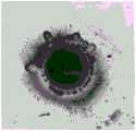
(2)适用于高深径比硬脆性复合材料的微孔加工;图1和图2为本发明中所加工成形通孔的照片;复合基板材料中单晶YIG膜典型厚度是50微米,单晶GGG基底的厚度是200微米;图1中设计孔径为100微米时,成形后实测孔径为100.57微米,图2设中计孔径为25微米时,成形后实测孔径为25.699微米,与预期偏差较小。(2) It is applicable to the micropore processing of high-depth-diameter ratio hard and brittle composite materials; Fig. 1 and Fig. 2 are the photos of the formed through holes processed in the present invention; the typical thickness of single crystal YIG film in the composite substrate material is 50 microns, single crystal The thickness of the GGG substrate is 200 microns; in Figure 1, when the designed pore diameter is 100 microns, the measured pore diameter after forming is 100.57 microns; when the designed pore diameter in Figure 2 is 25 microns, the measured pore diameter after forming is 25.699 microns, which has a small deviation from the expected .
(3)本发明能够对单晶YIG厚膜复合基板材料进行微孔加工,加工工艺具有稳定、效率高、精度高等优点,对于解决单晶YIG厚膜器件加工难及应用研究等问题具有重要的意义。(3) The present invention can process micropores on single crystal YIG thick-film composite substrate materials, and the processing technology has the advantages of stability, high efficiency, and high precision, and is of great importance for solving problems such as difficult processing of single crystal YIG thick-film devices and application research. significance.
本发明的其它优点、目标和特征将部分通过下面的说明体现,部分还将通过对本发明的研究和实践而为本领域的技术人员所理解。Other advantages, objectives and features of the present invention will partly be embodied through the following descriptions, and partly will be understood by those skilled in the art through the study and practice of the present invention.
附图说明:Description of drawings:
图1为本发明实施例1加工获得的微孔照片;Fig. 1 is the micropore photo that the embodiment of the present invention 1 processes and obtains;
图2为本发明实施例2加工获得的微孔照片。Fig. 2 is a photo of the micropores processed and obtained in Example 2 of the present invention.
具体实施方式:Detailed ways:
下面结合附图对本发明做进一步的详细说明,以令本领域技术人员参照说明书文字能够据以实施。The present invention will be further described in detail below in conjunction with the accompanying drawings, so that those skilled in the art can implement it with reference to the description.
应当理解,本文所使用的诸如“具有”、“包含”以及“包括”术语并不配出一个或多个其它元件或其组合的存在或添加。It should be understood that terms such as "having", "comprising" and "including" as used herein do not entail the presence or addition of one or more other elements or combinations thereof.
实施例1:Example 1:
被加工件:总厚度为300微米单晶钇铁石榴石铁氧体厚膜复合基板(即单晶YIG厚膜复合基板(YIG/GGG/YIG复合基板),其由钆镓石榴石基底层和钇铁石榴石生长层构成,即其结构为钇铁石榴石生长层/钆镓石榴石基底层/钇铁石榴石生长层(YIG/GGG/YIG),单晶钆镓石榴石(GGG)基底层厚度200微米,单晶钇铁石榴石(YIG)生长层厚度50微米;所成形孔的直径为100微米;Processed piece: single crystal yttrium iron garnet ferrite thick film composite substrate with a total thickness of 300 microns (that is, single crystal YIG thick film composite substrate (YIG/GGG/YIG composite substrate), which is composed of gadolinium gallium garnet base layer and Yttrium iron garnet growth layer composition, that is, its structure is Yttrium iron garnet growth layer/Gadolinium gallium garnet base layer/Yttrium iron garnet growth layer (YIG/GGG/YIG), single crystal Gadolinium gallium garnet (GGG) base The thickness of the bottom layer is 200 microns, and the thickness of the single crystal yttrium iron garnet (YIG) growth layer is 50 microns; the diameter of the formed hole is 100 microns;
一种单晶钇铁石榴石铁氧体厚膜复合基板上的微孔加工方法,包括以下步骤;A method for processing microholes on a single crystal yttrium iron garnet ferrite thick film composite substrate, comprising the following steps;
步骤一、单晶钇铁石榴石铁氧体厚膜复合基板的前处理:将YIG/GGG/YIG复合基板表面打磨抛光平整、抛光后用无水乙醇超声清洗10分钟,去除表面杂质和油污,最后用氮气吹干;Step 1. Pretreatment of single crystal yttrium-iron-garnet thick-film ferrite composite substrate: Grinding and polishing the surface of the YIG/GGG/YIG composite substrate to make it smooth. After polishing, use absolute ethanol to ultrasonically clean it for 10 minutes to remove surface impurities and oil stains. Finally blow dry with nitrogen;
步骤二、加工圆形通孔:采用全固态激光器输出1064nm的皮秒激光对前处理后的单晶YIG厚膜复合基板进行微孔加工,皮秒激光波长为1064nm,脉冲宽度为15ps,平均输出功率20W,重复频率100kHz,扫描速度为400mm/s;首先,以待成形孔中心为激光束起点,以螺旋状路径切除表面材料并逐渐达到成形孔径尺寸的~80%,并重复上述操作过程,逐层切除材料,直至得到贯通的粗加工孔,粗加工通孔孔径为成形孔孔径的~80%,并具有锥度;其次,采用沿轴线方向逐层切除的方式消除粗加工通孔中的锥度;以粗加工通孔的内表面为起点,激光束以螺旋状路径切除表面材料并逐渐达到成形孔径尺寸的~98%,并重复上述操作过程,逐层切除材料,直至消除粗加工通孔中的锥度;最后,对消除锥度的粗加工通孔表面进行逐层修整加工,去除表面粘结的残留材料和氧化层,获得与成形孔径基本一致的通孔;以消除锥度的通孔内表面为起点,激光束以环形路径切除表面材料并逐渐达到成形孔径尺寸;Step 2. Processing circular through-holes: Use all-solid-state lasers to output 1064nm picosecond lasers to process micro-holes on the single crystal YIG thick-film composite substrate after pretreatment. The picosecond laser wavelength is 1064nm, the pulse width is 15ps, and the average output The power is 20W, the repetition frequency is 100kHz, and the scanning speed is 400mm/s; first, the center of the hole to be formed is used as the starting point of the laser beam, and the surface material is removed in a spiral path until it reaches ~80% of the size of the formed hole, and the above operation process is repeated. The material is cut layer by layer until a through rough machining hole is obtained. The diameter of the rough machining hole is ~80% of the diameter of the forming hole and has a taper; secondly, the taper in the rough machining through hole is eliminated by cutting off layer by layer along the axial direction ; Starting from the inner surface of the rough-machined through-hole, the laser beam cuts off the surface material in a spiral path and gradually reaches ~98% of the formed aperture size, and repeats the above-mentioned operation process to remove material layer by layer until the rough-machined through-hole is eliminated. The taper; Finally, the surface of the rough-machined through-hole that eliminates the taper is trimmed layer by layer to remove the residual material and oxide layer bonded to the surface, and a through-hole that is basically the same as the formed aperture is obtained; the inner surface of the through-hole that eliminates the taper is Starting point, the laser beam ablates surface material in a circular path and gradually reaches the forming aperture size;
步骤三、对加工圆形通孔后的单晶钇铁石榴石铁氧体厚膜复合基板进行后处理:将单晶钇铁石榴石铁氧体厚膜复合基板在无水乙醇中超声清洗10分钟,消除表面和孔壁残留碎屑等杂质,并干燥后获得成形圆形通孔。Step 3: post-processing the single crystal yttrium iron garnet ferrite thick film composite substrate after the circular through hole is processed: ultrasonically clean the single crystal yttrium iron garnet ferrite thick film composite substrate in absolute ethanol for 10 Minutes to eliminate impurities such as residual debris on the surface and the hole wall, and obtain a shaped circular through hole after drying.
实施例2:Example 2:
被加工件:总厚度为250微米单晶钇铁石榴石铁氧体厚膜复合基板(即单晶YIG厚膜复合基板(YIG/GGG/YIG复合基板),其由钆镓石榴石基底层和钇铁石榴石生长层构成,即其结构为钇铁石榴石生长层/钆镓石榴石基底层/钇铁石榴石生长层(YIG/GGG/YIG),单晶钆镓石榴石(GGG)基底层厚度200微米,单晶钇铁石榴石(YIG)生长层厚度25微米;所成形孔的直径为25微米;Processed piece: single crystal yttrium iron garnet ferrite thick film composite substrate with a total thickness of 250 microns (that is, single crystal YIG thick film composite substrate (YIG/GGG/YIG composite substrate), which is composed of gadolinium gallium garnet base layer and Yttrium iron garnet growth layer composition, that is, its structure is Yttrium iron garnet growth layer/Gadolinium gallium garnet base layer/Yttrium iron garnet growth layer (YIG/GGG/YIG), single crystal Gadolinium gallium garnet (GGG) base The thickness of the bottom layer is 200 microns, and the thickness of the single crystal yttrium iron garnet (YIG) growth layer is 25 microns; the diameter of the formed hole is 25 microns;
一种单晶钇铁石榴石铁氧体厚膜复合基板上的微孔加工方法,包括以下步骤;A method for processing microholes on a single crystal yttrium iron garnet ferrite thick film composite substrate, comprising the following steps;
步骤一、单晶钇铁石榴石铁氧体厚膜复合基板的前处理:将YIG/GGG/YIG复合基板表面打磨抛光平整、抛光后用无水乙醇超声清洗10分钟,去除表面杂质和油污,最后用氮气吹干;Step 1. Pretreatment of single crystal yttrium-iron-garnet thick-film ferrite composite substrate: Grinding and polishing the surface of the YIG/GGG/YIG composite substrate to make it smooth. After polishing, use absolute ethanol to ultrasonically clean it for 10 minutes to remove surface impurities and oil stains. Finally blow dry with nitrogen;
步骤二、加工圆形通孔:采用全固态激光器输出1064nm的皮秒激光对前处理后的单晶YIG厚膜复合基板进行微孔加工,皮秒激光波长为1064nm,脉冲宽度为10ps,平均输出功率20W,重复频率100kHz,扫描速度为400mm/s;首先,以待成形孔中心为激光束起点,以螺旋状路径切除表面材料并逐渐达到成形孔径尺寸的~80%,并重复上述操作过程,逐层切除材料,直至得到贯通的粗加工孔,粗加工通孔孔径为成形孔孔径的~80%,并具有锥度;其次,采用沿轴线方向逐层切除的方式消除粗加工通孔中的锥度;以粗加工通孔的内表面为起点,激光束以螺旋状路径切除表面材料并逐渐达到成形孔径尺寸的~98%,并重复上述操作过程,逐层切除材料,直至消除粗加工通孔中的锥度;最后,对消除锥度的粗加工通孔表面进行逐层修整加工,去除表面粘结的残留材料和氧化层,获得与成形孔径基本一致的通孔;以消除锥度的通孔内表面为起点,激光束以环形路径切除表面材料并逐渐达到成形孔径尺寸;Step 2. Processing circular through-holes: Use all-solid-state lasers to output 1064nm picosecond lasers to process micro-holes on the pre-treated single crystal YIG thick film composite substrate. The picosecond laser wavelength is 1064nm, the pulse width is 10ps, and the average output The power is 20W, the repetition frequency is 100kHz, and the scanning speed is 400mm/s; first, the center of the hole to be formed is used as the starting point of the laser beam, and the surface material is removed in a spiral path until it reaches ~80% of the size of the formed hole, and the above operation process is repeated. The material is cut layer by layer until a through rough machining hole is obtained. The diameter of the rough machining hole is ~80% of the diameter of the forming hole and has a taper; secondly, the taper in the rough machining through hole is eliminated by cutting off layer by layer along the axial direction ; Starting from the inner surface of the rough-machined through-hole, the laser beam cuts off the surface material in a spiral path and gradually reaches ~98% of the formed aperture size, and repeats the above-mentioned operation process to remove material layer by layer until the rough-machined through-hole is eliminated. The taper; Finally, the surface of the rough-machined through-hole that eliminates the taper is trimmed layer by layer to remove the residual material and oxide layer bonded to the surface, and a through-hole that is basically the same as the formed aperture is obtained; the inner surface of the through-hole that eliminates the taper is Starting point, the laser beam ablates surface material in a circular path and gradually reaches the forming aperture size;
步骤三、对加工圆形通孔后的单晶钇铁石榴石铁氧体厚膜复合基板进行后处理:将单晶钇铁石榴石铁氧体厚膜复合基板在无水乙醇中超声清洗10分钟,消除表面和孔壁残留碎屑等杂质,并干燥后获得成形圆形通孔。Step 3: post-processing the single crystal yttrium iron garnet ferrite thick film composite substrate after the circular through hole is processed: ultrasonically clean the single crystal yttrium iron garnet ferrite thick film composite substrate in absolute ethanol for 10 Minutes to eliminate impurities such as residual debris on the surface and the hole wall, and obtain a shaped circular through hole after drying.
尽管本发明的实施方案已公开如上,但其并不仅仅限于说明书和实施方式中所列运用,它完全可以被适用于各种适合本发明的领域,对于熟悉本领域的人员而言,可容易地实现另外的修改,因此在不背离权利要求及等同范围所限定的一般概念下,本发明并不限于特定的细节和这里示出与描述的图例。Although the embodiment of the present invention has been disclosed as above, it is not limited to the use listed in the specification and implementation, it can be applied to various fields suitable for the present invention, and it can be easily understood by those skilled in the art Therefore, the invention is not limited to the specific details and examples shown and described herein without departing from the general concept defined by the claims and their equivalents.
Claims (7)
Translated fromChinesePriority Applications (1)
| Application Number | Priority Date | Filing Date | Title |
|---|---|---|---|
| CN202211375565.9ACN115647618A (en) | 2022-11-04 | 2022-11-04 | Method for processing micropores on monocrystal yttrium iron garnet ferrite thick film composite substrate |
Applications Claiming Priority (1)
| Application Number | Priority Date | Filing Date | Title |
|---|---|---|---|
| CN202211375565.9ACN115647618A (en) | 2022-11-04 | 2022-11-04 | Method for processing micropores on monocrystal yttrium iron garnet ferrite thick film composite substrate |
Publications (1)
| Publication Number | Publication Date |
|---|---|
| CN115647618Atrue CN115647618A (en) | 2023-01-31 |
Family
ID=84994776
Family Applications (1)
| Application Number | Title | Priority Date | Filing Date |
|---|---|---|---|
| CN202211375565.9APendingCN115647618A (en) | 2022-11-04 | 2022-11-04 | Method for processing micropores on monocrystal yttrium iron garnet ferrite thick film composite substrate |
Country Status (1)
| Country | Link |
|---|---|
| CN (1) | CN115647618A (en) |
Citations (7)
| Publication number | Priority date | Publication date | Assignee | Title |
|---|---|---|---|---|
| JP2007152374A (en)* | 2005-12-02 | 2007-06-21 | Fuji Electric Device Technology Co Ltd | Method for forming through hole in ferrite plate |
| CN103143841A (en)* | 2013-03-08 | 2013-06-12 | 西北工业大学 | Method for hole machining with picosecond laser |
| CN103537810A (en)* | 2012-07-16 | 2014-01-29 | 中国电子科技集团公司第九研究所 | Laser drilling technique for ferrite substrate |
| CN104607808A (en)* | 2014-12-11 | 2015-05-13 | 西北工业大学 | Method for machining micro holes in ceramic matrix composite through femtosecond lasers |
| CN110253161A (en)* | 2019-06-25 | 2019-09-20 | 西南应用磁学研究所 | A rapid laser through-hole method for spun ferrite substrates |
| CN111014960A (en)* | 2019-12-23 | 2020-04-17 | 武汉华工激光工程有限责任公司 | Ferrite straight hole processing system and processing method, ferrite and circuit substrate |
| CN114406500A (en)* | 2022-03-03 | 2022-04-29 | 广东华中科技大学工业技术研究院 | Laser cutting method for ferrite composite material |
- 2022
- 2022-11-04CNCN202211375565.9Apatent/CN115647618A/enactivePending
Patent Citations (7)
| Publication number | Priority date | Publication date | Assignee | Title |
|---|---|---|---|---|
| JP2007152374A (en)* | 2005-12-02 | 2007-06-21 | Fuji Electric Device Technology Co Ltd | Method for forming through hole in ferrite plate |
| CN103537810A (en)* | 2012-07-16 | 2014-01-29 | 中国电子科技集团公司第九研究所 | Laser drilling technique for ferrite substrate |
| CN103143841A (en)* | 2013-03-08 | 2013-06-12 | 西北工业大学 | Method for hole machining with picosecond laser |
| CN104607808A (en)* | 2014-12-11 | 2015-05-13 | 西北工业大学 | Method for machining micro holes in ceramic matrix composite through femtosecond lasers |
| CN110253161A (en)* | 2019-06-25 | 2019-09-20 | 西南应用磁学研究所 | A rapid laser through-hole method for spun ferrite substrates |
| CN111014960A (en)* | 2019-12-23 | 2020-04-17 | 武汉华工激光工程有限责任公司 | Ferrite straight hole processing system and processing method, ferrite and circuit substrate |
| CN114406500A (en)* | 2022-03-03 | 2022-04-29 | 广东华中科技大学工业技术研究院 | Laser cutting method for ferrite composite material |
Non-Patent Citations (2)
| Title |
|---|
| 荣烈润: "激光微细孔加工技术及其应用", 机电一体化, no. 06, pages 180 - 181* |
| 陈文等: "材料物理性能", 武汉理工大学出版社, pages: 130* |
Similar Documents
| Publication | Publication Date | Title |
|---|---|---|
| TWI780103B (en) | Elastic wave element and method of manufacturing the same | |
| CN110534474A (en) | The preparation method of film on substrate | |
| CN106252802A (en) | YIG band elimination filter based on planarization resonance coupled structure and manufacture method | |
| KR102392858B1 (en) | Toroidal Capacitor RF, Microwave, and Mm Wave Systems | |
| JP4334864B2 (en) | Thin plate crystal wafer and method for manufacturing crystal resonator | |
| CN115647618A (en) | Method for processing micropores on monocrystal yttrium iron garnet ferrite thick film composite substrate | |
| WO2019056350A1 (en) | Mems coaxial filter, and manufacturing method | |
| CN106487346A (en) | Body elasticity wave device and the manufacture method of body elasticity wave device | |
| CN103276360A (en) | Magnetic nanowire array thin film and preparation method thereof | |
| CN117359104A (en) | Chemical mechanical polishing method for silicon carbide crystal based on laser technology under liquid phase | |
| TW201742377A (en) | Baw device and BAW device manufacturing method | |
| CN1960053A (en) | High power efficiency plane microwave oscillator with low phase noise | |
| US20150159279A1 (en) | Process for obtaining a plurality of laminas made of a material having monocrystalline structure from an ingot | |
| CN101837515A (en) | Solar silicon cell nanosecond-pulse green laser scriber | |
| Nozhkin et al. | Improved laser microprocessing of 2D planar microstrip slow-wave structures for millimeter-band vacuum microelectronic devices | |
| He et al. | Microfabrication of a conformal microstrip angular log-periodic meander line TWT | |
| CN106399956B (en) | A kind of 4H-silicon carbide composite precious metal thin film and preparation method thereof | |
| Goka et al. | Experimental study of vibrations of mesa-shaped AT-cut quartz plates | |
| RU2117382C1 (en) | At-cur crystal element manufacturing process | |
| CN105699139A (en) | Preparation method of GaN thin film transmission electron microscope cross-section sample based on reactive ion etching | |
| CN120109015B (en) | Method for electroplating metal on back of wafer | |
| Van Kerckhoven et al. | A novel laser-assisted fabrication process for nanowired substrate integrated devices | |
| RU2377718C1 (en) | High-frequency filter at cut crystal resonator | |
| CN120415354A (en) | A method for preparing a single crystal piezoelectric thin film bulk acoustic resonator | |
| CN85101664A (en) | Tuned oscillator |
Legal Events
| Date | Code | Title | Description |
|---|---|---|---|
| PB01 | Publication | ||
| PB01 | Publication | ||
| SE01 | Entry into force of request for substantive examination | ||
| SE01 | Entry into force of request for substantive examination | ||
| RJ01 | Rejection of invention patent application after publication | ||
| RJ01 | Rejection of invention patent application after publication | Application publication date:20230131 |