CN115632076A - A detection device with broadband photoelectric response and its preparation method - Google Patents
A detection device with broadband photoelectric response and its preparation methodDownload PDFInfo
- Publication number
- CN115632076A CN115632076ACN202211312743.3ACN202211312743ACN115632076ACN 115632076 ACN115632076 ACN 115632076ACN 202211312743 ACN202211312743 ACN 202211312743ACN 115632076 ACN115632076 ACN 115632076A
- Authority
- CN
- China
- Prior art keywords
- thallium
- nickel
- selenide
- detection device
- selenium
- Prior art date
- Legal status (The legal status is an assumption and is not a legal conclusion. Google has not performed a legal analysis and makes no representation as to the accuracy of the status listed.)
- Pending
Links
Images


Classifications
- H—ELECTRICITY
- H10—SEMICONDUCTOR DEVICES; ELECTRIC SOLID-STATE DEVICES NOT OTHERWISE PROVIDED FOR
- H10F—INORGANIC SEMICONDUCTOR DEVICES SENSITIVE TO INFRARED RADIATION, LIGHT, ELECTROMAGNETIC RADIATION OF SHORTER WAVELENGTH OR CORPUSCULAR RADIATION
- H10F10/00—Individual photovoltaic cells, e.g. solar cells
- H10F10/10—Individual photovoltaic cells, e.g. solar cells having potential barriers
- H10F10/16—Photovoltaic cells having only PN heterojunction potential barriers
- B—PERFORMING OPERATIONS; TRANSPORTING
- B82—NANOTECHNOLOGY
- B82Y—SPECIFIC USES OR APPLICATIONS OF NANOSTRUCTURES; MEASUREMENT OR ANALYSIS OF NANOSTRUCTURES; MANUFACTURE OR TREATMENT OF NANOSTRUCTURES
- B82Y15/00—Nanotechnology for interacting, sensing or actuating, e.g. quantum dots as markers in protein assays or molecular motors
- H—ELECTRICITY
- H10—SEMICONDUCTOR DEVICES; ELECTRIC SOLID-STATE DEVICES NOT OTHERWISE PROVIDED FOR
- H10F—INORGANIC SEMICONDUCTOR DEVICES SENSITIVE TO INFRARED RADIATION, LIGHT, ELECTROMAGNETIC RADIATION OF SHORTER WAVELENGTH OR CORPUSCULAR RADIATION
- H10F71/00—Manufacture or treatment of devices covered by this subclass
- H—ELECTRICITY
- H10—SEMICONDUCTOR DEVICES; ELECTRIC SOLID-STATE DEVICES NOT OTHERWISE PROVIDED FOR
- H10F—INORGANIC SEMICONDUCTOR DEVICES SENSITIVE TO INFRARED RADIATION, LIGHT, ELECTROMAGNETIC RADIATION OF SHORTER WAVELENGTH OR CORPUSCULAR RADIATION
- H10F77/00—Constructional details of devices covered by this subclass
- H10F77/10—Semiconductor bodies
- H10F77/14—Shape of semiconductor bodies; Shapes, relative sizes or dispositions of semiconductor regions within semiconductor bodies
- H—ELECTRICITY
- H10—SEMICONDUCTOR DEVICES; ELECTRIC SOLID-STATE DEVICES NOT OTHERWISE PROVIDED FOR
- H10F—INORGANIC SEMICONDUCTOR DEVICES SENSITIVE TO INFRARED RADIATION, LIGHT, ELECTROMAGNETIC RADIATION OF SHORTER WAVELENGTH OR CORPUSCULAR RADIATION
- H10F77/00—Constructional details of devices covered by this subclass
- H10F77/20—Electrodes
- H10F77/206—Electrodes for devices having potential barriers
- Y—GENERAL TAGGING OF NEW TECHNOLOGICAL DEVELOPMENTS; GENERAL TAGGING OF CROSS-SECTIONAL TECHNOLOGIES SPANNING OVER SEVERAL SECTIONS OF THE IPC; TECHNICAL SUBJECTS COVERED BY FORMER USPC CROSS-REFERENCE ART COLLECTIONS [XRACs] AND DIGESTS
- Y02—TECHNOLOGIES OR APPLICATIONS FOR MITIGATION OR ADAPTATION AGAINST CLIMATE CHANGE
- Y02P—CLIMATE CHANGE MITIGATION TECHNOLOGIES IN THE PRODUCTION OR PROCESSING OF GOODS
- Y02P70/00—Climate change mitigation technologies in the production process for final industrial or consumer products
- Y02P70/50—Manufacturing or production processes characterised by the final manufactured product
Landscapes
- Chemical & Material Sciences (AREA)
- Engineering & Computer Science (AREA)
- Nanotechnology (AREA)
- Health & Medical Sciences (AREA)
- Life Sciences & Earth Sciences (AREA)
- General Health & Medical Sciences (AREA)
- Molecular Biology (AREA)
- Crystallography & Structural Chemistry (AREA)
- Light Receiving Elements (AREA)
Abstract
Description
Translated fromChinese技术领域technical field
本发明涉及一种光电探测器,具体是指一种具有宽频光电响应的探测器件及其制备方法。The invention relates to a photoelectric detector, in particular to a detection device with a wide-band photoelectric response and a preparation method thereof.
背景技术Background technique
现有技术中,已有的各种半导体光电探测器件,由于受到自身半导体带隙宽度的限制,只能用于单波段的光电探测,一般存在响应范围比较窄的问题和不足,如紫外光波段、可见光波段、近红外波段和中红外波段,使器件的适用范围减小。近年来,具有宽谱带响应的光电探测器件的研制受到了国内外众多研究人员的广泛关注,主要原因为:通过对不同波段光的响应分析及对比,可以有效避免外在条件的信号干扰,大幅提高器件光信号传播和接收的准确性。In the prior art, the existing various semiconductor photodetection devices can only be used for single-band photodetection due to the limitation of their own semiconductor bandgap width, and generally have the problem and deficiency of a relatively narrow response range, such as the ultraviolet band , visible light band, near-infrared band and mid-infrared band, which reduces the applicable range of the device. In recent years, the development of photodetector devices with wide-band response has attracted extensive attention from many researchers at home and abroad. The main reason is that through the analysis and comparison of responses to different bands of light, signal interference from external conditions can be effectively avoided. Greatly improve the accuracy of device optical signal transmission and reception.
随着光电探测器应用范围的逐步扩大,对高性能光电探测器的需求,特别是对覆盖多波段响应的超宽带光电探测器的需求日益增加。迄今为止,基于硅、碲镉汞和铟镓砷等材料的光电探测器在实际应用中占据了主要市场。然而,这些化合物具有毒性,合成难度大,且受低温的工作温度的限制。并且这些传统半导体与衬底之间的晶格不匹配问题进一步阻碍了它们在便携、可集成和柔性器件中的应用。With the gradual expansion of the application range of photodetectors, the demand for high-performance photodetectors, especially for ultra-broadband photodetectors covering multi-band responses is increasing. To date, photodetectors based on materials such as silicon, mercury cadmium telluride, and indium gallium arsenide have dominated the market in practical applications. However, these compounds are toxic, difficult to synthesize, and limited by low working temperature. And the lattice mismatch problem between these traditional semiconductors and substrates further hinders their application in portable, integrable, and flexible devices.
近年来,具有片层结构的二维半导体材料已成为传统半导体材料的替代品或补充。基于二维材料的光电探测器因其原子级薄的厚度、连续可调谐的带隙、优异的力学性能和光电性能得到了迅速的发展。自从石墨烯被发现以来,越来越多的二维材料例如二硫化钼、过渡金属二卤化物、黑磷等被广泛地应用于光电探测,由于其显著的电学、光学和热性能优势,在光电器件、光催化、能源和其他领域方面具有广泛的应用前景,引起了人们密切的关注。二维层状材料可以在整个电磁光谱中设计柔性光电纳米器件,已广泛应用于光电探测器,在性能、响应率等方面有了很大的突破。然而,基于二维材料的探测器具有带隙大、光吸收弱、载流子寿命短等问题,因此迫切需要高响应、稳定、窄带隙的超宽带光活性材料,以实现广泛的宽带、低功耗和高性能探测器。In recent years, two-dimensional semiconductor materials with a lamellar structure have become a substitute or supplement to traditional semiconductor materials. Photodetectors based on 2D materials have been rapidly developed due to their atomically thin thickness, continuously tunable bandgap, and excellent mechanical and optoelectronic properties. Since the discovery of graphene, more and more two-dimensional materials such as molybdenum disulfide, transition metal dichalcogenides, black phosphorus, etc. have been widely used in photodetection. It has broad application prospects in photoelectric devices, photocatalysis, energy and other fields, and has attracted people's close attention. Two-dimensional layered materials allow the design of flexible optoelectronic nanodevices across the entire electromagnetic spectrum, and have been widely used in photodetectors with great breakthroughs in performance and responsivity. However, detectors based on two-dimensional materials have problems such as large band gap, weak light absorption, and short carrier lifetime. Therefore, ultra-broadband photoactive materials with high response, stability, and narrow band gap are urgently needed to achieve a wide range of broadband, low power consumption and high performance detectors.
铊镍硒是近年来备受关注的三元硫属化合物之一,但其研究却出奇的少。铊镍硒是一种由弱范德华相互作用叠加而成的层状化合物,在体态下表现出0.36eV窄带隙的直接带隙结构。不同于过渡金属二卤族化合物,当扩展到单层时,铊镍硒不会经历从直接带隙结构到间接带隙结构的转变,保持了直接带隙特性。这一特性使铊镍硒具有高的载流子密度和良好的光吸收效率,是一种有前途的电子和光电子器件的候选材料。然而,薄层的二维材料表现出非常低效的光子捕获,这阻碍了高性能光电器件的应用,特别是难以实现高响应和低能耗的器件。Thallium nickel selenium is one of the ternary chalcogenides that has attracted much attention in recent years, but its research is surprisingly little. TlNiSe is a layered compound formed by the superposition of weak van der Waals interactions, and exhibits a direct bandgap structure with a narrow bandgap of 0.36eV in the bulk state. Unlike transition metal dichalcogenides, TlNiSe does not undergo a transition from direct to indirect bandgap structure when extended to a single layer, maintaining the direct bandgap property. This property makes thallium nickel selenide a promising candidate material for electronic and optoelectronic devices with high carrier density and good light absorption efficiency. However, thin layers of 2D materials exhibit very inefficient photon harvesting, which hinders the application of high-performance optoelectronic devices, especially those that are difficult to achieve with high response and low energy consumption.
发明内容Contents of the invention
为解决现有技术的问题,本发明的第一个目的是提供一种具有宽频光电响应的半金属铊镍硒材料复合结构的探测器件。In order to solve the problems of the prior art, the first object of the present invention is to provide a detection device with a semi-metallic thallium-nickel-selenium composite structure with a wide-band photoelectric response.
为此,本发明的上述目的通过以下技术方案实现:For this reason, above-mentioned purpose of the present invention is achieved through the following technical solutions:
一种具有宽频光电响应的探测器件,其特征在于:所述探测器自下而上设置有:电绝缘基底、铊镍硒纳米片和源、漏电极,铊镍硒纳米片上端的两侧是源、漏电极层,铊镍硒纳米片作为光敏导电沟道,源、漏电极层与相应的引线电极相连用于连接外部测试电路,A detection device with a broadband photoelectric response, characterized in that: the detector is provided with: an electrically insulating substrate, a thallium-nickel-selenide nanosheet, and source and drain electrodes from bottom to top, and the two sides of the upper end of the thallium-nickel-selenide nanosheet are The source and drain electrode layers, the thallium nickel selenium nanosheets are used as photosensitive conductive channels, the source and drain electrode layers are connected to the corresponding lead electrodes for connecting external test circuits,
所述电绝缘基底包括本征高阻硅衬底及其上覆盖的二氧化硅层,所述本征高阻硅衬底的电阻率为10000Ω·cm,厚度为300μm;所述二氧化硅层覆盖在本征高阻硅衬底上,厚度为300nm,The electrical insulating substrate includes an intrinsic high-resistance silicon substrate and a silicon dioxide layer covered thereon, the resistivity of the intrinsic high-resistance silicon substrate is 10000Ω·cm, and the thickness is 300 μm; the silicon dioxide layer Covered on the intrinsic high resistance silicon substrate, the thickness is 300nm,
所述的铊镍硒纳米片为机械剥离的单分子层,厚度为10nm,The thallium-nickel-selenium nanosheets are mechanically exfoliated monolayers with a thickness of 10nm.
所述的源、漏电极为金属复合电极,通过紫外光刻技术和电子束蒸发技术制作,下层金属为铬以作为粘附层,厚度是5nm,上层金属为金,厚度是70nm,The source and drain electrodes are metal composite electrodes, which are made by ultraviolet lithography technology and electron beam evaporation technology. The lower metal is chromium as an adhesion layer with a thickness of 5nm, and the upper metal is gold with a thickness of 70nm.
所述引线电极厚度为200~400nm。The thickness of the lead electrode is 200-400nm.
在采用上述技术方案的同时,本发明还可以采用或者组合采用如下技术方案:While adopting the above technical solutions, the present invention can also adopt or combine the following technical solutions:
作为本发明的优选技术方案:所述的源、漏电极整体大小为220μm×140μm。As a preferred technical solution of the present invention: the overall size of the source and drain electrodes is 220 μm×140 μm.
作为本发明的优选技术方案:铊镍硒纳米片的一侧上端设置石墨烯层,石墨烯层与铊镍硒纳米片通过片层间范德华力粘合。As a preferred technical solution of the present invention: a graphene layer is arranged on one side of the thallium-nickel-selenide nanosheet, and the graphene layer and the thallium-nickel-selenide nanosheet are bonded by van der Waals force between the sheets.
作为本发明的优选技术方案:所述石墨烯层厚度为2nm。As a preferred technical solution of the present invention: the thickness of the graphene layer is 2nm.
作为本发明的优选技术方案:所述铊镍硒纳米片的一侧的上端设置硒化铋层,硒化铋层与铊镍硒纳米片搭建异质结结构。As a preferred technical solution of the present invention: a bismuth selenide layer is arranged on one side of the thallium-nickel-selenide nanosheet, and the bismuth selenide layer and the thallium-nickel-selenide nanosheet build a heterojunction structure.
作为本发明的优选技术方案:硒化铋层厚度为40nm。As a preferred technical solution of the present invention: the thickness of the bismuth selenide layer is 40nm.
本发明的第二个目的是提供一种具有宽频光电响应的探测器件的制备方法。The second object of the present invention is to provide a method for preparing a detection device with a wide-band photoelectric response.
为此,本发明的上述目的通过以下技术方案实现:For this reason, above-mentioned purpose of the present invention is achieved through the following technical solutions:
包括以下步骤:Include the following steps:
S1,使用丙酮、异丙醇、乙醇和去离子水将覆盖硅和二氧化硅的衬底进行表面超声清洗,通过精密切割技术将衬底切成1cm×1cm的样品;S1, use acetone, isopropanol, ethanol and deionized water to ultrasonically clean the surface of the substrate covered with silicon and silicon dioxide, and cut the substrate into 1cm×1cm samples by precision cutting technology;
S2,通过转移平台微区定位方法,使用蓝胶胶带将沉积生长的铊镍硒纳米片进行机械剥离,利用干法转移技术转移到S1生成的衬底上,进行编号定位标记;S2, using the blue glue tape to mechanically peel off the deposited and grown thallium-nickel-selenide nanosheets by using the micro-region positioning method of the transfer platform, and transfer them to the substrate generated by S1 using the dry transfer technology, and perform numbering and positioning marking;
S3,使用热板烘烤以及匀胶机匀胶涂覆,使光刻胶AZ5214均匀附着在S1制备的衬底和铊镍硒纳米片材料上;S3, use a hot plate to bake and coat with a coater, so that the photoresist AZ5214 is evenly attached to the substrate prepared in S1 and the thallium-nickel-selenium nanosheet material;
S4,结合使用紫外光刻、电子束蒸发法及传统剥离工艺制备与铊镍硒纳米片接触的源、漏电极,形成良好的接触;S4, combined use of ultraviolet lithography, electron beam evaporation method and traditional lift-off process to prepare source and drain electrodes in contact with thallium nickel selenium nanosheets to form good contact;
S5,最后,采用标准的半导体封装技术,把器件贴到PCB底座上,引线,简单封装完成复合结构的探测器件的制备。S5. Finally, standard semiconductor packaging technology is used to paste the device on the PCB base, lead wires, and simply package to complete the preparation of the detection device of the composite structure.
在采用上述技术方案的同时,本发明还可以采用或者组合采用如下技术方案:While adopting the above technical solutions, the present invention can also adopt or combine the following technical solutions:
作为本发明的优选技术方案:As preferred technical scheme of the present invention:
还包括以下步骤:Also includes the following steps:
在步骤S2基础上,将机械剥离的石墨烯层转移到衬底和铊镍硒接触形成结区;On the basis of step S2, transfer the mechanically exfoliated graphene layer to the substrate and form a junction region in contact with thallium nickel selenium;
在采用上述技术方案的同时,本发明还可以采用或者组合采用如下技术方案:While adopting the above technical solutions, the present invention can also adopt or combine the following technical solutions:
作为本发明的优选技术方案:还包括以下步骤:As preferred technical scheme of the present invention: also comprise the following steps:
在步骤S2基础上,将机械剥离的硒化铋层转移到衬底和铊镍硒接触形成异质结。On the basis of step S2, the mechanically stripped bismuth selenide layer is transferred to the substrate and is in contact with thallium nickel selenide to form a heterojunction.
与现有技术相比,本发明所提供的一种具有宽频光电响应的探测器件及其制备方法,利用载流子迁移率高且能带可调的铊镍硒材料作为光敏导电沟道,当铊镍硒薄片缩小到单分子层时不会发生从直接带隙结构到间接带隙结构的转变,保持了0.36eV的直接带隙特性,铊镍硒对称结构器件可以在室温下实现从可见光到中波红外的快速宽波段探测;利用金属与铊镍硒纳米片接触处的显著光伏效应,通过一组铊镍硒-石墨烯范德华接触和金属-铊镍硒肖特基接触组成的非对称性接触器件,打破了对称器件的金属-铊镍硒之间内建电场的镜像对称性,使得器件镜像电流无法相互抵消而对外产生了大的净光电流,实现了室温下器件的高响应光电探测;利用铊镍硒材料和表面为金属态的硒化铋材料搭建范德华异质结构,使得电子迁移率变大,缓解了原子薄二维材料的缺点。通过垂直堆叠结构,在实现上述非对称性接触的同时,实现了势垒的非对称,大的电势差进一步增加净的光电流,提高了器件的性能。Compared with the prior art, the present invention provides a detection device with broadband photoelectric response and its preparation method, which uses thallium nickel selenide material with high carrier mobility and adjustable energy band as the photosensitive conductive channel. When the thallium-nickel-selenium flake is reduced to a single molecular layer, there will be no transition from the direct bandgap structure to the indirect bandgap structure, and the direct bandgap characteristic of 0.36eV is maintained. The thallium-nickel-selenium symmetric structure device can be realized at room temperature from the visible light to the indirect bandgap structure. Fast broadband detection of mid-wave infrared; using the significant photovoltaic effect at the contact between metal and thallium-nickel-selenide nanosheets, through the asymmetry of a set of thallium-nickel-selenide-graphene van der Waals contacts and metal-thallium-nickel-selenide Schottky contacts The contact device breaks the mirror symmetry of the built-in electric field between the metal-thallium nickel selenide of the symmetrical device, so that the mirror current of the device cannot cancel each other out and generate a large net photocurrent, realizing the high response photodetection of the device at room temperature ;Using thallium nickel selenide materials and bismuth selenide materials with a metallic surface to build a van der Waals heterostructure, which increases the electron mobility and alleviates the shortcomings of atomically thin two-dimensional materials. Through the vertical stacking structure, while realizing the above-mentioned asymmetric contact, the asymmetry of the potential barrier is realized, and the large potential difference further increases the net photocurrent and improves the performance of the device.
附图说明Description of drawings
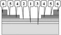
图1为本发明实施例1铊镍硒对称结构光电探测器的前侧示意图;Fig. 1 is the front schematic diagram of the thallium-nickel-selenium symmetrical structure photodetector of
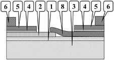
图2为本发明实施例2铊镍硒非对称结构光电探测器的前侧示意图;Fig. 2 is a front schematic diagram of a thallium-nickel-selenide asymmetric structure photodetector according to
图3为本发明实施例3铊镍硒和硒化铋异质结结构光电探测器的前侧示意图;Fig. 3 is a front side schematic diagram of a photodetector with a heterojunction structure of thallium nickel selenide and bismuth selenide in Example 3 of the present invention;
图4为本发明实施例1铊镍硒对称结构光电探测器在1V偏置电压下,对可见光638nm,近红外1550nm和中波红外4600nm的响应波形图;Fig. 4 is a response waveform diagram of a thallium-nickel-selenium symmetrical structure photodetector in Example 1 of the present invention to visible light 638nm, near-infrared 1550nm and mid-wave infrared 4600nm under a bias voltage of 1V;
图5为本发明实施例2铊镍硒非对称结构光电探测器在1V偏置电压下,对可见光638nm,近红外1550nm和中波红外4600nm的响应波形图;Fig. 5 is a response waveform diagram of a thallium-nickel-selenide asymmetric structure photodetector in Example 2 of the present invention to visible light 638nm, near-infrared 1550nm and mid-wave infrared 4600nm under a bias voltage of 1V;
图6为本发明实施例3铊镍硒和硒化铋异质结结构光电探测器在1V偏置电压下,对可见光638nm,近红外1550nm和中波红外4600nm的响应波形图;Fig. 6 is the response waveform diagram of visible light 638nm, near-infrared 1550nm and mid-wave infrared 4600nm for a photodetector with a heterojunction structure of thallium-nickel-selenide and bismuth-selenide in Example 3 of the present invention under a bias voltage of 1V;
图7为本发明实施例2铊镍硒和石墨烯非对称结构光电探测器在没有任何偏置电压下,在可见光638nm激光扫描二维光敏面时所产生的非对称性光电流分布图;Fig. 7 is an asymmetric photocurrent distribution diagram generated when a visible light 638nm laser scans a two-dimensional photosensitive surface without any bias voltage for a thallium nickel selenide and graphene asymmetric structure photodetector in Example 2 of the present invention;
图8为本发明实施例1对比的铊镍硒对称结构光电探测器在没有任何偏置电压下,在可见光638nm激光扫描二维光敏面时所产生的对称性光电流分布图;Fig. 8 is a symmetrical photocurrent distribution diagram generated when the visible light 638nm laser scans the two-dimensional photosensitive surface without any bias voltage for the thallium-nickel-selenium symmetrical structure photodetector compared with Example 1 of the present invention;
图9为本发明铊镍硒光电探测器、铊镍硒非对称性结构光电探测器以及铊镍硒和硒化铋异质结结构光电探测器在近红外1550nm的响应率对比图;Fig. 9 is a comparison chart of the responsivity of the thallium nickel selenide photodetector, the thallium nickel selenium asymmetric structure photodetector and the thallium nickel selenide and bismuth selenide heterojunction photodetector in the near infrared 1550nm of the present invention;
附图中,二氧化硅层1,铊镍硒纳米片2,本征高阻硅衬底3,源、漏铬电极4,源、漏金电极5,引线电极6,石墨烯层7,硒化铋层8。In the accompanying drawings,
具体实施方式:Detailed ways:
以下结合附图及实施例,对本发明的具体实施方式进行详述,以便发明技术方案易于理解、掌握。Below in conjunction with the accompanying drawings and embodiments, the specific implementation of the present invention will be described in detail, so that the technical solution of the invention can be easily understood and grasped.
参见图1、图2以及图3,本发明的一种具有宽频光电响应的探测器件,在本征高阻硅衬底3上是二氧化硅层2,在二氧化硅层2上是铊镍硒纳米片1,在铊镍硒纳米片1两端是金属源、漏电极,金属源、漏电极包括源、漏铬电极4和源、漏金电极5,最后,源、漏电极与相应的引线电极6相连用于连接电路。Referring to Fig. 1, Fig. 2 and Fig. 3, a kind of detection device with broadband photoelectric response of the present invention, on intrinsic high
所述本征高阻硅衬底3是本征高阻硅,其电阻率为10000Ω·cm,厚度为300μm;覆盖其上的是二氧化硅层2,厚度为300nm;The intrinsic high-
所述的铊镍硒纳米片1为薄层材料,厚度为10nm;The thallium-nickel-
所述的源、漏电极为金属复合电极,整体大小为220μm×140μm,下层金属为源、漏铬电极4,作为粘附层,厚度是5nm,上层金属为源、漏金电极5,厚度是70nm;相应的引线电极6,厚度为200~400nm;The source and drain electrodes are metal composite electrodes, the overall size is 220 μm × 140 μm, the lower metal is the source and drain
本发明的上述目的,是通过以下技术方案制作完成的。The above-mentioned purpose of the present invention is accomplished through the following technical solutions.
(1)首先使用丙酮、异丙醇、乙醇和去离子水将覆盖二氧化硅的硅衬底进行表面超声清洗,通过精密切割技术将衬底切成1cm×1cm的样品;(1) First, use acetone, isopropanol, ethanol and deionized water to ultrasonically clean the surface of the silicon substrate covered with silicon dioxide, and cut the substrate into 1cm×1cm samples by precision cutting technology;
(2)通过转移平台微区定位方法,使用蓝胶胶带将沉积生长的铊镍硒进行机械剥离,利用干法转移技术转移到上述衬底上,进行编号定位标记;(2) Using the micro-area positioning method of the transfer platform, the deposited and grown thallium nickel selenium was mechanically peeled off using blue glue tape, and transferred to the above substrate by dry transfer technology, and numbered and positioned;
(3)使用热板烘烤以及匀胶机匀胶涂覆,使光刻胶AZ5214均匀附着在上述衬底和铊镍硒材料上;(3) Baking on a hot plate and uniform coating with a coating machine, so that the photoresist AZ5214 is evenly attached to the above-mentioned substrate and the thallium-nickel-selenium material;
(4)结合使用紫外光刻、电子束蒸发法及传统剥离工艺制备与铊镍硒接触的源、漏电极,形成良好的接触;(4) Combined use of ultraviolet lithography, electron beam evaporation method and traditional stripping process to prepare source and drain electrodes in contact with thallium nickel selenium to form good contact;
(5)最后,采用标准的半导体封装技术,把器件贴到PCB底座上,引线,简单封装完成制备复合结构的探测器件。(5) Finally, standard semiconductor packaging technology is used to paste the device on the PCB base, lead wires, and simply package to complete the preparation of the detection device with a composite structure.
本发明的一种具有宽频光电响应的探测器件及其制备方法,是一种具有宽频光电响应的半金属铊镍硒材料复合结构的探测器件,制备方法包括如下步骤,将机械剥离的具有高迁移率的铊镍硒纳米片为基本结构单元转移到硅和二氧化硅衬底上,然后利用紫外光刻技术和电子束蒸发技术制作源、漏电极,通过超声引线等工艺制备出高灵敏超宽带探测的铊镍硒光电探测器。并且一组具有铊镍硒-石墨烯范德华接触与金属-铊镍硒肖特基接触组成非对称结构的探测器来打破器件的镜像电流。此外,通过引入拓扑绝缘体硒化铋与铊镍硒搭建异质结结构进行调控,在实现上述非对称性接触的同时,实现了势垒的非对称,大的电势差进一步增加净的光电流,提升器件的性能。本发明的具有宽频光电响应的探测器件利用铊镍硒纳米片的光电探测器具有高响应率、可见到中波红外光电探测、空气稳定性、集成度高、工艺成熟及可重复性等优点,在通信、光电子等领域具备应用前景,为实现室温下宽带且多功能性的光电探测研究奠定器件与理论基础。A detection device with a broadband photoelectric response and a preparation method thereof of the present invention is a detection device with a composite structure of a semi-metallic thallium nickel selenium material with a broadband photoelectric response. The preparation method includes the following steps: High-efficiency thallium-nickel-selenium nanosheets are transferred to silicon and silicon dioxide substrates as basic structural units, and then the source and drain electrodes are fabricated using ultraviolet lithography technology and electron beam evaporation technology, and high-sensitivity ultra-wideband electrodes are prepared by ultrasonic lead-through and other processes. Detection of thallium nickel selenide photodetectors. And a group of detectors with an asymmetric structure composed of thallium-nickel-selenide-graphene van der Waals contact and metal-thallium-nickel-selenium Schottky contact to break the mirror current of the device. In addition, by introducing topological insulators bismuth selenide and thallium nickel selenide to build a heterojunction structure for regulation, while realizing the above-mentioned asymmetric contact, the asymmetry of the potential barrier is realized, and the large potential difference further increases the net photocurrent and improves device performance. The detection device with broadband photoelectric response of the present invention utilizes the photodetector of thallium nickel selenium nanosheets to have the advantages of high responsivity, visible to mid-wave infrared photoelectric detection, air stability, high integration, mature process and repeatability, etc. It has application prospects in communication, optoelectronics and other fields, and lays a device and theoretical foundation for the realization of broadband and multifunctional photodetection research at room temperature.
具体制备和测试流程如下:The specific preparation and testing process is as follows:
步骤1首先使用丙酮、异丙醇、乙醇和去离子水将覆盖二氧化硅的硅衬底进行表面超声清洗,通过精密切割技术将衬底切成长宽为1cm×1cm的样品;Step 1: First, use acetone, isopropanol, ethanol, and deionized water to ultrasonically clean the surface of the silicon substrate covered with silicon dioxide, and cut the substrate into samples with a length and width of 1cm×1cm by precision cutting technology;
步骤2通过转移平台微区定位方法,使用蓝胶胶带将沉积生长的铊镍硒纳米片进行机械剥离,利用干法转移技术转移到上述衬底上,进行编号定位标记;
步骤3转移所得到的铊镍硒纳米片,利用拉曼光谱对铊镍硒的物理特性进行了表征。利用原子力显微镜(AFM)、扫描电子显微镜(SEM)和能量色散X射线光谱(EDS)对铊镍硒样品微观形貌进行表征。The obtained thallium-nickel-selenium nanosheets were transferred in
步骤4使用热板烘烤以及匀胶机匀胶涂覆,使光刻胶AZ5214均匀附着在上述衬底和铊镍硒材料上;Step 4: Baking on a hot plate and uniform coating with a coating machine, so that the photoresist AZ5214 is evenly attached to the above substrate and the thallium nickel selenium material;
步骤5结合使用紫外光刻、电子束蒸发法及传统剥离工艺制备与铊镍硒接触的源、漏电极;Step 5: Combining ultraviolet lithography, electron beam evaporation and traditional lift-off process to prepare source and drain electrodes in contact with thallium nickel selenium;
步骤6最后,采用标准的半导体封装技术,把器件贴到PCB底座上,引线,简单封装完成制备集成的复合结构的探测器件。
本发明的一种具有宽频光电响应的探测器件及其制备方法,复合结构可以缓解薄层二维材料的缺点,由高载流子迁移率的石墨烯和表面态为金属态的拓扑绝缘体硒化铋和铊镍硒搭建的复合结构,具有制备简单、势垒非对称和光电流大等优点。A detection device with a broadband photoelectric response and a preparation method thereof of the present invention, the composite structure can alleviate the shortcomings of thin-layer two-dimensional materials, and is selenized by graphene with high carrier mobility and a topological insulator whose surface state is a metal state The composite structure built by bismuth and thallium nickel selenium has the advantages of simple preparation, asymmetric potential barrier and large photocurrent.
实施例1Example 1
如图1所示,本发明的一种具有宽频光电响应的探测器,覆盖介质层二氧化硅为300nm,其下硅衬底的厚度300μm;铊镍硒纳米片的厚度约为10nm,源、漏电极层整体尺寸为:长220μm,宽140μm,沟道长度为6μm;源、漏复合电极厚度为75nm,相应的引线电极6厚度200~400nm,源、漏电极与相应的引线电极6相连用于连接电路;首先在可见光638nm,近红外1550nm和中波红外4600nm的波长范围下测试了器件的光电响应,图4为偏置电压为1V时测量的铊镍硒对称结构的光电探测器的波形图,结果说明本发明提供的具有宽频光电响应的探测器件,铊镍硒对称结构的太赫兹光电探测器可以实现可见光到中波红外范围内的宽谱高灵敏探测。图8为纯材料铊镍硒对称性结构的探测器,激光扫描对称性的器件时所产生的光电流呈现明显的镜像对称,光响应电流靠近金属与铊镍硒材料两边的区域,幅值和区域只有微弱的差别,而两个区域光响应电流极性方向具有明显相反的方向。As shown in Fig. 1, a kind of detector with broadband photoelectric response of the present invention, covering dielectric layer silicon dioxide is 300nm, the thickness of silicon substrate under it is 300 μ m; The overall size of the drain electrode layer is: 220 μm in length, 140 μm in width, and 6 μm in channel length; the thickness of the source and drain composite electrodes is 75 nm, and the thickness of the
实施例2Example 2
如图2所示,本发明的具有宽频光电响应的探测器件,覆盖氧化硅的硅衬底的厚度为300μm;铊镍硒纳米片的厚度约为10nm,石墨烯层厚度为2nm,电极整体尺寸为:长220μm,宽140μm,沟道长度为6μm;源、漏复合电极厚度为75nm,相应的引线电极厚度200~400nm,源、漏电极与相应的引线电极相连用于连接电路。图5展示了偏置电压为1V时测量的铊镍硒非对称结构光电探测器的波形图,结果说明本发明提供的铊镍硒太赫兹光电探测器可以实现可见光到中波红外范围内的宽谱高灵敏探测。As shown in Figure 2, the detection device with broadband photoelectric response of the present invention, the thickness of the silicon substrate covered with silicon oxide is 300 μ m; It is: 220 μm in length, 140 μm in width, and 6 μm in channel length; the thickness of the source and drain compound electrodes is 75 nm, and the thickness of the corresponding lead electrodes is 200 to 400 nm. The source and drain electrodes are connected to the corresponding lead electrodes for connecting circuits. Figure 5 shows the waveform diagram of the thallium-nickel-selenium asymmetric structure photodetector measured when the bias voltage is 1V. The results show that the thallium-nickel-selenide terahertz photodetector provided by the present invention can realize a wide range from visible light to mid-wave infrared. Spectrum highly sensitive detection.
如图7所示是实施例2的非对称性设计结构探测器件在没有任何偏置电压下,在可见光638nm激光扫描二维光敏面时所产生的光电流分布图呈现着非对称性,光响应电流更靠近于一边金属与铊镍硒材料接触区域;石墨烯层的介入让探测器具有非对称性接触,打破了相互抵消的镜像光电流,极大地提高了净光响应电流。与图8纯材料铊镍硒对称性结构的探测器的光电流扫描图形成明显对比。As shown in Figure 7, the photocurrent distribution graph generated when the visible light 638nm laser scans the two-dimensional photosensitive surface of the detector device with an asymmetric design structure in Example 2 without any bias voltage presents asymmetry, and the photoresponse The current is closer to the contact area between the metal and the thallium-nickel-selenium material; the intervention of the graphene layer makes the detector have an asymmetric contact, which breaks the mirror photocurrent that cancels each other out, and greatly improves the net photoresponse current. It is in obvious contrast with the photocurrent scan pattern of the detector with the symmetric structure of pure material thallium nickel selenium in Fig. 8 .
实施例3Example 3
如图3所示,本发明的具有宽频光电响应的探测器件,覆盖氧化硅的硅衬底的厚度为300μm;铊镍硒纳米片的厚度约为10nm,硒化铋层厚度为40nm,电极整体尺寸为:长220μm,宽140μm,沟道长度为6μm;源、漏复合电极厚度为75nm,相应的引线电极厚度200~400nm,源、漏电极与相应的引线电极相连用于连接电路。As shown in Figure 3, in the detection device with broadband photoelectric response of the present invention, the thickness of the silicon substrate covered with silicon oxide is 300 μm; the thickness of the thallium nickel selenide nanosheet is about 10 nm, and the thickness of the bismuth selenide layer is 40 nm. The dimensions are: length 220 μm, width 140 μm,
图6分别展示了偏置电压为1V时测量的铊镍硒和硒化铋异质结构光电探测器的波形图,结果说明本发明提供的铊镍硒和硒化铋异质结构可以实现可见光到中波红外范围内的宽谱高灵敏探测。Figure 6 shows the waveform diagrams of the thallium-nickel-selenide and bismuth-selenide heterostructure photodetectors measured when the bias voltage is 1V, and the results show that the thallium-nickel-selenide and bismuth-selenide heterostructures provided by the present invention can realize visible light to Broad-spectrum high-sensitivity detection in the mid-wave infrared range.
如图9所示,本发明通过对比实施例1、实施例2和本实施例3的探测器件在近红外1550nm的响应率大小,可以看出从铊镍硒对称结构光电探测器,到铊镍硒非对称结构光电探测器以及铊镍硒和硒化铋异质结构光电探测器,器件响应率有了数量级的提升。结果说明本发明提供的通过非对称结构和异质结结构产生定向电场来增大响应电流,来提高器件的探测能力的方法是合理的、有效的。As shown in Figure 9, the present invention compares the responsivity of the detector devices of Example 1, Example 2 and Example 3 in the near-infrared 1550nm. Selenium asymmetric structure photodetectors and thallium nickel selenide and bismuth selenide heterostructure photodetectors have an order of magnitude improvement in device responsivity. The results show that the method provided by the present invention to increase the response current by generating an directional electric field through the asymmetric structure and the heterojunction structure to improve the detection capability of the device is reasonable and effective.
本发明的一种具有宽频光电响应的探测器件及其制备方法,器件中的光电流、响应率等各种参数在一定范围内变化,利用载流子迁移率高且能带可调的铊镍硒材料作为光敏导电沟道,实现在室温下实现从可见光到中波红外的快速宽波段探测。分别引入石墨烯层和硒化铋层,进一步构建了具有铊镍硒-石墨烯范德华接触与金属-铊镍硒肖特基接触的非对称结构的探测器来打破器件的镜像电流,打破了相互抵消的镜像光电流,极大地提高了净光响应电流。此外,通过引入拓扑绝缘体硒化铋与铊镍硒搭建异质结结构进行调控,在实现上述非对称性接触的同时,实现了势垒的非对称,大的电势差进一步增加净的光电流,提升了器件的性能。本发明的优点是基于铊镍硒纳米片的光电探测器,具有高响应率、可见到中波红外的宽带光电探测、空气稳定性高、集成度高、工艺成熟及可重复性等优点。本发明中的具有宽频光电响应的探测器件在电子和光电子领域具有潜在的应用前景,为实现室温下高灵敏且多功能性的光电探测研究奠定器件与理论基础。A detection device with broadband photoelectric response and its preparation method of the present invention, various parameters such as photocurrent and responsivity in the device change within a certain range, and thallium nickel with high carrier mobility and adjustable energy band is used The selenium material is used as a photosensitive conductive channel to realize fast broadband detection from visible light to mid-wave infrared at room temperature. The graphene layer and the bismuth selenide layer were introduced respectively, and a detector with an asymmetric structure of thallium nickel selenide-graphene van der Waals contact and metal-thallium nickel selenide Schottky contact was further constructed to break the mirror current of the device and break the mutual The offset mirrored photocurrent greatly improves the net photoresponse current. In addition, by introducing topological insulators bismuth selenide and thallium nickel selenide to build a heterojunction structure for regulation, while realizing the above-mentioned asymmetric contact, the asymmetry of the potential barrier is realized, and the large potential difference further increases the net photocurrent and improves performance of the device. The invention has the advantages of a photodetector based on thallium nickel selenium nanosheets, which has the advantages of high responsivity, broadband photodetection from visible to mid-wave infrared, high air stability, high integration, mature technology and repeatability. The detection device with broadband photoelectric response in the present invention has potential application prospects in the fields of electronics and optoelectronics, and lays a device and theoretical foundation for realizing high-sensitivity and multi-functional photodetection research at room temperature.
Claims (9)
Translated fromChinesePriority Applications (2)
| Application Number | Priority Date | Filing Date | Title |
|---|---|---|---|
| CN202211312743.3ACN115632076A (en) | 2022-10-25 | 2022-10-25 | A detection device with broadband photoelectric response and its preparation method |
| CN202310359356.3ACN116130529B (en) | 2022-10-25 | 2023-04-06 | Detection device with broadband photoelectric response and preparation method thereof |
Applications Claiming Priority (1)
| Application Number | Priority Date | Filing Date | Title |
|---|---|---|---|
| CN202211312743.3ACN115632076A (en) | 2022-10-25 | 2022-10-25 | A detection device with broadband photoelectric response and its preparation method |
Publications (1)
| Publication Number | Publication Date |
|---|---|
| CN115632076Atrue CN115632076A (en) | 2023-01-20 |
Family
ID=84907094
Family Applications (2)
| Application Number | Title | Priority Date | Filing Date |
|---|---|---|---|
| CN202211312743.3APendingCN115632076A (en) | 2022-10-25 | 2022-10-25 | A detection device with broadband photoelectric response and its preparation method |
| CN202310359356.3AActiveCN116130529B (en) | 2022-10-25 | 2023-04-06 | Detection device with broadband photoelectric response and preparation method thereof |
Family Applications After (1)
| Application Number | Title | Priority Date | Filing Date |
|---|---|---|---|
| CN202310359356.3AActiveCN116130529B (en) | 2022-10-25 | 2023-04-06 | Detection device with broadband photoelectric response and preparation method thereof |
Country Status (1)
| Country | Link |
|---|---|
| CN (2) | CN115632076A (en) |
Cited By (1)
| Publication number | Priority date | Publication date | Assignee | Title |
|---|---|---|---|---|
| CN119050191A (en)* | 2024-10-29 | 2024-11-29 | 电子科技大学长三角研究院(湖州) | Ultra-wideband high-sensitivity photo-thermal electric detector |
Families Citing this family (1)
| Publication number | Priority date | Publication date | Assignee | Title |
|---|---|---|---|---|
| CN118099262A (en)* | 2024-04-10 | 2024-05-28 | 国科大杭州高等研究院 | A room temperature broadband high performance photoelectric detection and communication detector and its application |
Family Cites Families (10)
| Publication number | Priority date | Publication date | Assignee | Title |
|---|---|---|---|---|
| WO2014053855A1 (en)* | 2012-10-05 | 2014-04-10 | The University Court Of The University Of Edinburgh | Microelectrode for molten salts |
| CN106206636B (en)* | 2016-08-16 | 2019-05-03 | 京东方科技集团股份有限公司 | A kind of X-ray detection panel and preparation method thereof |
| WO2018039962A1 (en)* | 2016-08-31 | 2018-03-08 | Boe Technology Group Co., Ltd. | Radiation detector and fabricating method thereof |
| CN110770555A (en)* | 2017-04-20 | 2020-02-07 | 特里纳米克斯股份有限公司 | Optical detector |
| CN107946401A (en)* | 2017-08-30 | 2018-04-20 | 中国科学院上海技术物理研究所 | A kind of room temperature topological insulator terahertz detector and preparation method |
| EP3939092A1 (en)* | 2019-03-15 | 2022-01-19 | trinamiX GmbH | Optical sensor, method for selecting an optical sensor and detector for optical detection |
| CN110993720B (en)* | 2019-10-25 | 2022-07-26 | 深圳瀚光科技有限公司 | Rapid photoelectric detector based on graphene/black phosphorus/molybdenum disulfide/graphene heterojunction and preparation method thereof |
| CN111389442B (en)* | 2020-04-20 | 2021-12-28 | 苏州大学 | P-N heterojunction composite material loaded on surface of foamed nickel and preparation method and application thereof |
| CN114784125B (en)* | 2022-03-25 | 2024-04-02 | 国科大杭州高等研究院 | An asymmetry-induced room temperature highly sensitive photodetector device and its preparation method |
| CN115050846A (en)* | 2022-06-10 | 2022-09-13 | 南京理工大学 | MoS 2 /Ta 2 NiSe 5 Heterojunction photoelectric detector and preparation method thereof |
- 2022
- 2022-10-25CNCN202211312743.3Apatent/CN115632076A/enactivePending
- 2023
- 2023-04-06CNCN202310359356.3Apatent/CN116130529B/enactiveActive
Cited By (1)
| Publication number | Priority date | Publication date | Assignee | Title |
|---|---|---|---|---|
| CN119050191A (en)* | 2024-10-29 | 2024-11-29 | 电子科技大学长三角研究院(湖州) | Ultra-wideband high-sensitivity photo-thermal electric detector |
Also Published As
| Publication number | Publication date |
|---|---|
| CN116130529A (en) | 2023-05-16 |
| CN116130529B (en) | 2023-08-01 |
Similar Documents
| Publication | Publication Date | Title |
|---|---|---|
| Zeng et al. | Uncooled mid-infrared sensing enabled by chip-integrated low-temperature-grown 2D PdTe2 Dirac semimetal | |
| Zeng et al. | Graphene/PtSe 2/pyramid Si Van der Waals schottky junction for room-temperature broadband infrared light detection | |
| Wu et al. | A defect-induced broadband photodetector based on WS 2/pyramid Si 2D/3D mixed-dimensional heterojunction with a light confinement effect | |
| Wang et al. | Enhanced rectification, transport property and photocurrent generation of multilayer ReSe2/MoS2 p–n heterojunctions | |
| CN116130529B (en) | Detection device with broadband photoelectric response and preparation method thereof | |
| Singh et al. | Defect-mediated transport in self-powered, broadband, and ultrafast photoresponse of a MoS2/AlN/Si-based photodetector | |
| Wu et al. | Defect-induced broadband photodetection of layered γ-In 2 Se 3 nanofilm and its application in near infrared image sensors | |
| Wang et al. | Type-I heterostructure based on WS2/PtS2 for high-performance photodetectors | |
| Li et al. | In situ construction of PtSe2/Ge Schottky junction array with interface passivation for broadband infrared photodetection and imaging | |
| CN114784128B (en) | A topologically enhanced antimony telluride terahertz photodetector based on a butterfly antenna structure and its preparation method | |
| Singh et al. | Temperature-dependent electrical transport and optoelectronic properties of SnS2/p-Si heterojunction | |
| CN111739964B (en) | Two-dimensional semiconductor photodetector with double gate structure and preparation method thereof | |
| KR101848319B1 (en) | Transparent Photoelectric Element and Method for fabricating the same | |
| Li et al. | Broadband InSb/Si heterojunction photodetector with graphene transparent electrode | |
| CN108281493B (en) | Tungsten diselenide and metal vertical Schottky junction self-driven photodetector and its fabrication | |
| Liang et al. | Self-powered Bi2Se3/Si position-sensitive detector and its performance enhancement by introducing a Si nanopyramid structure | |
| Gu et al. | Large-area, flexible, and dual-source co-evaporated Cs3Cu2I5 nanolayer to construct ultra-broadband photothermoelectric detector from visible to terahertz | |
| Li et al. | Mixed-dimensional PtSe2/Bi2Te3/pyramid Si heterojunction with a light-trapping structure for highly sensitive ultrabroadband photodetection | |
| Kang et al. | High-performance light trajectory tracking and image sensing devices based on a γ-In 2 Se 3/GaAs heterostructure | |
| Mondal et al. | Ultrafast and ultrabroadband UV–Vis-NIR photosensitivity under reverse and self-bias conditions by n+-ZnO/n-Si isotype heterojunction with> 1 kHz bandwidth | |
| Zhang et al. | Air-stable self-driven UV photodetectors on controllable lead-free CsCu2I3 microwire arrays | |
| JP5540323B2 (en) | Schottky junction element, photoelectric conversion element and solar cell using the same | |
| Shin et al. | Graphene/WS2/LaVO3 heterojunction for self-powered, high-speed, and broadband photodetectors | |
| CN116995127B (en) | A controllable black arsenic field effect tube, photodetector and its application | |
| Chen et al. | A high-performance broadband phototransistor array of a PdSe 2/SOI Schottky junction |
Legal Events
| Date | Code | Title | Description |
|---|---|---|---|
| PB01 | Publication | ||
| PB01 | Publication | ||
| SE01 | Entry into force of request for substantive examination | ||
| SE01 | Entry into force of request for substantive examination | ||
| WD01 | Invention patent application deemed withdrawn after publication | ||
| WD01 | Invention patent application deemed withdrawn after publication | Application publication date:20230120 |