CN115604590A - Image signal processor, operation method of image signal processor, and image sensor device including image signal processor - Google Patents
Image signal processor, operation method of image signal processor, and image sensor device including image signal processorDownload PDFInfo
- Publication number
- CN115604590A CN115604590ACN202210791868.2ACN202210791868ACN115604590ACN 115604590 ACN115604590 ACN 115604590ACN 202210791868 ACN202210791868 ACN 202210791868ACN 115604590 ACN115604590 ACN 115604590A
- Authority
- CN
- China
- Prior art keywords
- image
- signal processor
- image signal
- domain processing
- generate
- Prior art date
- Legal status (The legal status is an assumption and is not a legal conclusion. Google has not performed a legal analysis and makes no representation as to the accuracy of the status listed.)
- Pending
Links
Images


Classifications
- H—ELECTRICITY
- H04—ELECTRIC COMMUNICATION TECHNIQUE
- H04N—PICTORIAL COMMUNICATION, e.g. TELEVISION
- H04N25/00—Circuitry of solid-state image sensors [SSIS]; Control thereof
- H04N25/40—Extracting pixel data from image sensors by controlling scanning circuits, e.g. by modifying the number of pixels sampled or to be sampled
- H04N25/46—Extracting pixel data from image sensors by controlling scanning circuits, e.g. by modifying the number of pixels sampled or to be sampled by combining or binning pixels
- H—ELECTRICITY
- H04—ELECTRIC COMMUNICATION TECHNIQUE
- H04N—PICTORIAL COMMUNICATION, e.g. TELEVISION
- H04N23/00—Cameras or camera modules comprising electronic image sensors; Control thereof
- H04N23/45—Cameras or camera modules comprising electronic image sensors; Control thereof for generating image signals from two or more image sensors being of different type or operating in different modes, e.g. with a CMOS sensor for moving images in combination with a charge-coupled device [CCD] for still images
- G—PHYSICS
- G06—COMPUTING OR CALCULATING; COUNTING
- G06T—IMAGE DATA PROCESSING OR GENERATION, IN GENERAL
- G06T5/00—Image enhancement or restoration
- G06T5/50—Image enhancement or restoration using two or more images, e.g. averaging or subtraction
- G—PHYSICS
- G06—COMPUTING OR CALCULATING; COUNTING
- G06T—IMAGE DATA PROCESSING OR GENERATION, IN GENERAL
- G06T5/00—Image enhancement or restoration
- G06T5/70—Denoising; Smoothing
- G—PHYSICS
- G06—COMPUTING OR CALCULATING; COUNTING
- G06T—IMAGE DATA PROCESSING OR GENERATION, IN GENERAL
- G06T7/00—Image analysis
- G06T7/10—Segmentation; Edge detection
- H—ELECTRICITY
- H04—ELECTRIC COMMUNICATION TECHNIQUE
- H04N—PICTORIAL COMMUNICATION, e.g. TELEVISION
- H04N23/00—Cameras or camera modules comprising electronic image sensors; Control thereof
- H04N23/60—Control of cameras or camera modules
- H04N23/665—Control of cameras or camera modules involving internal camera communication with the image sensor, e.g. synchronising or multiplexing SSIS control signals
- H—ELECTRICITY
- H04—ELECTRIC COMMUNICATION TECHNIQUE
- H04N—PICTORIAL COMMUNICATION, e.g. TELEVISION
- H04N23/00—Cameras or camera modules comprising electronic image sensors; Control thereof
- H04N23/95—Computational photography systems, e.g. light-field imaging systems
- H04N23/951—Computational photography systems, e.g. light-field imaging systems by using two or more images to influence resolution, frame rate or aspect ratio
- H—ELECTRICITY
- H04—ELECTRIC COMMUNICATION TECHNIQUE
- H04N—PICTORIAL COMMUNICATION, e.g. TELEVISION
- H04N25/00—Circuitry of solid-state image sensors [SSIS]; Control thereof
- H04N25/70—SSIS architectures; Circuits associated therewith
- H04N25/71—Charge-coupled device [CCD] sensors; Charge-transfer registers specially adapted for CCD sensors
- H04N25/75—Circuitry for providing, modifying or processing image signals from the pixel array
- H—ELECTRICITY
- H04—ELECTRIC COMMUNICATION TECHNIQUE
- H04N—PICTORIAL COMMUNICATION, e.g. TELEVISION
- H04N9/00—Details of colour television systems
- H04N9/64—Circuits for processing colour signals
- G—PHYSICS
- G06—COMPUTING OR CALCULATING; COUNTING
- G06T—IMAGE DATA PROCESSING OR GENERATION, IN GENERAL
- G06T2207/00—Indexing scheme for image analysis or image enhancement
- G06T2207/10—Image acquisition modality
- G06T2207/10024—Color image
- G—PHYSICS
- G06—COMPUTING OR CALCULATING; COUNTING
- G06T—IMAGE DATA PROCESSING OR GENERATION, IN GENERAL
- G06T2207/00—Indexing scheme for image analysis or image enhancement
- G06T2207/20—Special algorithmic details
- G06T2207/20016—Hierarchical, coarse-to-fine, multiscale or multiresolution image processing; Pyramid transform
- G—PHYSICS
- G06—COMPUTING OR CALCULATING; COUNTING
- G06T—IMAGE DATA PROCESSING OR GENERATION, IN GENERAL
- G06T2207/00—Indexing scheme for image analysis or image enhancement
- G06T2207/20—Special algorithmic details
- G06T2207/20112—Image segmentation details
- G06T2207/20132—Image cropping
- G—PHYSICS
- G06—COMPUTING OR CALCULATING; COUNTING
- G06T—IMAGE DATA PROCESSING OR GENERATION, IN GENERAL
- G06T2207/00—Indexing scheme for image analysis or image enhancement
- G06T2207/20—Special algorithmic details
- G06T2207/20212—Image combination
- G06T2207/20216—Image averaging
Landscapes
- Engineering & Computer Science (AREA)
- Multimedia (AREA)
- Signal Processing (AREA)
- Theoretical Computer Science (AREA)
- Physics & Mathematics (AREA)
- General Physics & Mathematics (AREA)
- Human Computer Interaction (AREA)
- Computer Vision & Pattern Recognition (AREA)
- Computing Systems (AREA)
- Image Processing (AREA)
- Facsimile Image Signal Circuits (AREA)
Abstract
Description
Translated fromChinese相关申请的交叉引用Cross References to Related Applications
本申请要求于2021年7月7日在韩国知识产权局提交的韩国专利申请No.10-2021-0088960和于2021年12月21日在韩国知识产权局提交的韩国专利申请No.10-2021-0183767的优先权,所述申请的全部公开内容通过引用合并于此。This application claims Korean Patent Application No. 10-2021-0088960 filed with the Korean Intellectual Property Office on July 7, 2021 and Korean Patent Application No. 10-2021 filed with the Korean Intellectual Property Office on December 21, 2021 - Priority of 0183767, the entire disclosure of said application is hereby incorporated by reference.
技术领域technical field
本文描述的本发明构思的实施例涉及图像系统,更具体地涉及图像信号处理器、图像信号处理器的操作方法和包括图像信号处理器的图像传感器设备。Embodiments of the inventive concept described herein relate to an image system, and more particularly, to an image signal processor, an operating method of the image signal processor, and an image sensor device including the image signal processor.
背景技术Background technique
智能电话、平板电脑、个人计算机(PC)或数码相机中包括的图像传感器通过将从外部对象反射的光转换为电信号来获得关于外部对象的图像信息。执行各种图像信号处理操作以将从图像传感器获得的电信号转换为人可感知的图像信息和/或提高图像质量。An image sensor included in a smartphone, a tablet, a personal computer (PC), or a digital camera obtains image information about an external object by converting light reflected from the external object into an electrical signal. Various image signal processing operations are performed to convert electrical signals obtained from image sensors into human-perceivable image information and/or to improve image quality.
发明内容Contents of the invention
本公开的实施例提供一种具有提高的性能和降低的功耗的图像信号处理器、该图像信号处理器的操作方法以及包括该图像信号处理器的图像传感器设备。Embodiments of the present disclosure provide an image signal processor having improved performance and reduced power consumption, an operating method of the image signal processor, and an image sensor device including the image signal processor.
根据实施例,一种图像信号装置包括存储器和通信地耦接到存储器的图像信号处理器。图像信号处理器被配置为使图像信号装置从第一图像传感器设备接收第一输入图像。图像信号处理器还被配置为进一步使图像信号装置对第一输入图像执行合并和裁剪操作以生成第一图像。图像信号处理器还被配置为进一步使图像信号装置对第一图像执行拜耳域处理以生成第二图像。图像信号处理器还被配置为进一步使图像信号装置对第二图像执行RGB域处理以生成第三图像。图像信号处理器还被配置为进一步使图像信号装置对第三图像执行YUV域处理以生成输出图像。YUV域处理包括以下至少一种:空间去噪操作、时间去噪操作、运动补偿操作、色调映射操作、细节增强操作和锐化操作。According to an embodiment, an image signal device includes a memory and an image signal processor communicatively coupled to the memory. The image signal processor is configured to cause the image signal arrangement to receive a first input image from a first image sensor device. The image signal processor is further configured to further cause the image signal device to perform combining and cropping operations on the first input image to generate the first image. The image signal processor is further configured to further cause the image signal device to perform Bayer domain processing on the first image to generate the second image. The image signal processor is further configured to further cause the image signal device to perform RGB domain processing on the second image to generate a third image. The image signal processor is further configured to further cause the image signal device to perform YUV domain processing on the third image to generate an output image. The YUV domain processing includes at least one of the following: spatial denoising operation, temporal denoising operation, motion compensation operation, tone mapping operation, detail enhancement operation and sharpening operation.
根据实施例,图像信号处理器的操作方法包括从图像传感器设备接收输入图像。该操作方法还包括对输入图像执行合并和裁剪操作以生成第一图像。该操作方法还包括对第一图像执行拜耳域处理以生成第二图像。该操作方法还包括对第二图像执行RGB域处理以生成第三图像。该操作方法还包括对第三图像执行YUV域处理以生成输出图像。执行YUV域处理包括输出所述输出图像。第二图像的分辨率与第三图像的分辨率匹配。YUV域处理包括以下至少一种:空间去噪操作、时间去噪操作、运动补偿操作、色调映射操作、细节增强操作和锐化操作。According to an embodiment, a method of operating an image signal processor includes receiving an input image from an image sensor device. The method of operation also includes performing a merging and cropping operation on the input images to generate the first image. The method of operation also includes performing Bayer domain processing on the first image to generate the second image. The method of operation also includes performing RGB domain processing on the second image to generate a third image. The method of operation also includes performing YUV domain processing on the third image to generate an output image. Performing YUV domain processing includes outputting the output image. The resolution of the second image matches the resolution of the third image. The YUV domain processing includes at least one of the following: spatial denoising operation, temporal denoising operation, motion compensation operation, tone mapping operation, detail enhancement operation and sharpening operation.
根据实施例,一种图像传感器设备包括:像素阵列,包括多个像素;行驱动器,控制多个像素;模数转换器,将像素信号转换为数字信号;输出缓冲器,基于数字信号对输入图像进行输出;以及图像信号处理器,被配置为基于输入图像生成输出图像。图像信号处理器还被配置为基于输入图像生成帧(frame)信息。图像信号处理器还被配置为对输入图像执行合并和裁剪操作以生成第一图像。图像信号处理器还被配置为基于帧信息对第一图像执行拜耳域处理以生成第二图像。图像信号处理器还被配置为基于帧信息对第二图像执行RGB域处理以生成第三图像。图像信号处理器还被配置为基于帧信息对第三图像执行YUV域处理以生成输出图像。YUV域处理包括以下至少一种:空间去噪操作、时间去噪操作、运动补偿操作、色调映射操作、细节增强操作和锐化操作。According to an embodiment, an image sensor device includes: a pixel array including a plurality of pixels; a row driver controlling the plurality of pixels; an analog-to-digital converter converting pixel signals into digital signals; an output buffer for processing an input image based on the digital signals outputting; and an image signal processor configured to generate an output image based on the input image. The image signal processor is also configured to generate frame information based on the input image. The image signal processor is also configured to perform merging and cropping operations on the input images to generate the first image. The image signal processor is further configured to perform Bayer domain processing on the first image based on the frame information to generate a second image. The image signal processor is further configured to perform RGB domain processing on the second image based on the frame information to generate a third image. The image signal processor is further configured to perform YUV domain processing on the third image based on the frame information to generate an output image. The YUV domain processing includes at least one of the following: spatial denoising operation, temporal denoising operation, motion compensation operation, tone mapping operation, detail enhancement operation and sharpening operation.
附图说明Description of drawings
通过参照附图详细描述本公开的实施例,本公开的上述及其他目的和特征将变得显而易见。The above and other objects and features of the present disclosure will become apparent by describing the embodiments of the present disclosure in detail with reference to the accompanying drawings.
图1是示出了根据本公开的实施例的图像系统的框图。FIG. 1 is a block diagram showing an image system according to an embodiment of the present disclosure.
图2是示出了图1的图像信号处理器的架构的框图。FIG. 2 is a block diagram showing the architecture of the image signal processor of FIG. 1 .
图3是示出了图2的图像信号处理器的操作的流程图。FIG. 3 is a flowchart illustrating the operation of the image signal processor of FIG. 2 .
图4是示出了图像信号处理器的架构的框图。FIG. 4 is a block diagram showing the architecture of an image signal processor.
图5是示出了图4的图像信号处理器的操作的流程图。FIG. 5 is a flowchart illustrating the operation of the image signal processor of FIG. 4 .
图6是示出了图1的图像信号处理器的的框图。FIG. 6 is a block diagram illustrating the image signal processor of FIG. 1 .
图7是示出了图1的图像信号处理器的的框图。FIG. 7 is a block diagram illustrating the image signal processor of FIG. 1 .
图8是示出了图1的图像传感器设备的框图。FIG. 8 is a block diagram illustrating the image sensor device of FIG. 1 .
图9是示出了根据本公开的实施例的图像传感器设备的框图。FIG. 9 is a block diagram illustrating an image sensor device according to an embodiment of the present disclosure.
图10是示出了根据本公开的实施例的图像传感器设备的框图。FIG. 10 is a block diagram illustrating an image sensor device according to an embodiment of the present disclosure.
图11是用于描述根据本公开的实施例的图像传感器设备的堆叠结构的图。FIG. 11 is a diagram for describing a stack structure of an image sensor device according to an embodiment of the present disclosure.
图12是示出了根据本公开的实施例的图像系统的框图。FIG. 12 is a block diagram illustrating an image system according to an embodiment of the present disclosure.
图13是用于描述图12的图像信号处理器的框图。FIG. 13 is a block diagram for describing the image signal processor of FIG. 12 .
图14是示出了根据本公开的实施例的图像系统的框图。FIG. 14 is a block diagram illustrating an image system according to an embodiment of the present disclosure.
图15是示出了根据本公开的实施例的图像系统的框图。FIG. 15 is a block diagram illustrating an image system according to an embodiment of the present disclosure.
图16是包括多相机模块的电子设备的框图。FIG. 16 is a block diagram of an electronic device including a multi-camera module.
图17是图16的相机模块的详细框图。FIG. 17 is a detailed block diagram of the camera module of FIG. 16 .
图18是示出应用了根据本公开的实施例的图像设备的系统的图。FIG. 18 is a diagram illustrating a system to which an image device according to an embodiment of the present disclosure is applied.
具体实施方式detailed description
下面可以以使本领域普通技术人员容易实现本公开的程度详细并清楚地描述本公开的实施例。在以下描述中,术语“块”、“单元”、“模块”等或与所述术语相对应的组件可以以软件、硬件或其组合的形式来实现。Embodiments of the present disclosure will be described in detail and clearly below in such a degree that those of ordinary skill in the art can easily realize the present disclosure. In the following description, the terms 'block', 'unit', 'module', etc. or components corresponding to the terms may be implemented in the form of software, hardware or a combination thereof.
图1是示出了根据本公开的实施例的图像系统的框图。参考图1,图像系统100包括图像传感器设备110、图像信号处理器(ISP)120和存储设备130。图像系统100可以包括在各种计算系统中,例如台式计算机、膝上型计算机、平板计算机、智能电话、可穿戴设备、黑匣子和数码相机。FIG. 1 is a block diagram showing an image system according to an embodiment of the present disclosure. Referring to FIG. 1 , an
图像传感器设备110可以基于从外部入射的光来生成图像数据。例如,图像传感器设备110可以包括多个像素。多个像素中的每一个可以被配置为输出与从外部入射的光相对应的电信号。图像传感器设备110可以基于电信号输出图像数据。在实施例中,由图像传感器设备110生成的图像数据可以作为输入图像IMG_in提供给图像信号处理器120。The
图像信号处理器120可以从图像传感器设备110接收输入图像IMG_in。图像信号处理器120可以对接收的输入图像IMG_in执行各种信号处理操作以生成输出图像IMG_out。例如,图像信号处理器120可以执行各种图像信号处理操作,例如去噪操作、色调映射操作、细节增强操作、白平衡操作、伽马校正操作、去马赛克(de-mosaic)操作、锐化操作和颜色转换操作。The
在实施例中,从图像传感器设备110输出的输入图像IMG_in的域或颜色图案可以与从图像信号处理器120输出的输出图像IMG_out的域或颜色图案不同。例如,从图像传感器设备110输出的输入图像IMG_in的域或颜色图案可以是BYR域(拜耳域(Bayer Domain)),而从图像信号处理器120输出的输出图像IMG_out的域或颜色图案可以是YUV域。In an embodiment, the domain or color pattern of the input image IMG_in output from the
在实施例中,从图像传感器设备110输出的输入图像IMG_in的域或颜色图案可以与图像传感器设备110的滤色器阵列(CFA)的域或颜色图案相同(例如匹配)。从图像传感器设备110输出的输入图像IMG_in的大小(例如,分辨率)可以与从图像信号处理器120输出的输出图像IMG_out的大小(例如,分辨率)不同。In an embodiment, the domain or color pattern of the input image IMG_in output from the
在实施例中,图像信号处理器120可以通过改变输入图像IMG_in的域和大小来执行上述的各种图像信号处理操作。将参照以下附图详细描述根据本公开的实施例的图像信号处理器120的操作。In an embodiment, the
存储设备130可以被配置为存储由图像信号处理器120使用的各种数据、各种信息或各种图像数据。在实施例中,存储设备130可以是高速存储设备,例如动态随机存取存储器(DRAM)。The
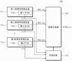
图2是示出了图1的图像信号处理器的架构的框图。图3是示出了图2的图像信号处理器的操作的流程图。参考图1、图2和图3,第一图像信号处理器120_a可以包括合并和裁剪模块121_a、第一拜耳(BYR)域处理模块122_a、第二BYR域处理模块123_a、RGB域处理模块124_a和YUV域处理模块125_a。FIG. 2 is a block diagram showing the architecture of the image signal processor of FIG. 1 . FIG. 3 is a flowchart illustrating the operation of the image signal processor of FIG. 2 . Referring to FIG. 1, FIG. 2 and FIG. 3, the first image signal processor 120_a may include a merge and crop module 121_a, a first Bayer (BYR) domain processing module 122_a, a second BYR domain processing module 123_a, an RGB domain processing module 124_a and YUV domain processing module 125_a.
在图3的操作S110中,第一图像信号处理器120_a可以接收输入图像IMG_in。例如,第一图像信号处理器120_a可以直接从图像传感器设备110接收输入图像IMG_in。备选地或附加地,图像传感器设备110可以将输入图像IMG_in存储在存储设备130中,并且第一图像信号处理器120_a可以访问存储设备130以读取输入图像IMG_in。In operation S110 of FIG. 3 , the first image signal processor 120_a may receive an input image IMG_in. For example, the first image signal processor 120_a may directly receive the input image IMG_in from the
在实施例中,输入图像IMG_in的颜色图案或域可以是BYR域。然而,本公开不限于此。例如,输入图像IMG_in可以具有与图像传感器设备110的滤色器阵列(CFA)的颜色图案相同(例如,匹配)的颜色图案或域(例如,BYR域、四域、九域、六域或十域)。In an embodiment, the color pattern or domain of the input image IMG_in may be a BYR domain. However, the present disclosure is not limited thereto. For example, the input image IMG_in may have a color pattern or field (e.g., BYR field, four field, nine field, six field, or ten area).
在图3的操作S120中,第一图像信号处理器120_a可以通过对输入图像IMG_in执行合并和裁剪操作来生成第a图像IMG_a。例如,第一图像信号处理器120_a的合并和裁剪模块121_a可以通过对输入图像IMG_in执行合并和裁剪操作来生成第a图像IMG_a。在实施例中,第a图像IMG_a可以具有BYR域或拜耳颜色图案。例如,在输入图像IMG_in是BYR域的情况下,第a图像IMG_a可以具有BYR域而无需单独的合成操作。备选地或附加地,在输入图像IMG_in不是BYR域(例如,四域、九域、六域或十域)的情况下,可以通过合并和裁剪模块121_a对输入图像IMG_in的合成操作来使第a图像IMG_a具有BYR域。In operation S120 of FIG. 3 , the first image signal processor 120_a may generate an a-th image IMG_a by performing combining and cropping operations on the input image IMG_in. For example, the merging and cropping module 121_a of the first image signal processor 120_a may generate the a-th image IMG_a by performing a merging and cropping operation on the input image IMG_in. In an embodiment, the ath image IMG_a may have a BYR domain or a Bayer color pattern. For example, in case the input image IMG_in is the BYR domain, the a-th image IMG_a may have the BYR domain without a separate compositing operation. Alternatively or additionally, in the case that the input image IMG_in is not a BYR domain (for example, four domains, nine domains, six domains or ten domains), it is possible to make the first The a image IMG_a has a BYR field.
在实施例中,第a图像IMG_a的大小可以小于或等于输入图像IMG_in的大小。例如,合并和裁剪模块121_a可以通过对输入图像IMG_in的裁剪操作将输入图像IMG_in的特定区域确定为第a图像IMG_a。由合并和裁剪模块121_a生成的第a图像IMG_a可以被传送到第一BYR域处理模块122_a。In an embodiment, the size of the a-th image IMG_a may be smaller than or equal to the size of the input image IMG_in. For example, the merging and cropping module 121_a may determine a specific area of the input image IMG_in as the a-th image IMG_a through a cropping operation on the input image IMG_in. The a-th image IMG_a generated by the merging and cropping module 121_a may be transferred to the first BYR domain processing module 122_a.
在图3的操作S130中,第一图像信号处理器120_a可以通过对第a图像IMG_a执行第一BYR域处理来生成第b图像IMG_b和第a帧信息FI_a。例如,第一图像信号处理器120_a的第一BYR域处理模块122_a可以基于第a图像IMG_a来提取第a帧信息FI_a。第a帧信息FI_a可以包括用于图像信号处理操作的信息,例如,与输入图像IMG_in的帧(例如,完整帧或整个帧)或每个区域(例如,帧或输入图像的一部分)有关的图像金字塔信息、每个区域的平均/分布/直方图信息、或运动信息。这样生成的第a帧信息FI_a可以存储在存储设备130中。In operation S130 of FIG. 3 , the first image signal processor 120_a may generate a b-th image IMG_b and a-th frame information FI_a by performing a first BYR domain process on the a-th image IMG_a. For example, the first BYR domain processing module 122_a of the first image signal processor 120_a may extract the ath frame information FI_a based on the ath image IMG_a. The a-th frame information FI_a may include information for an image signal processing operation, for example, an image related to a frame (for example, a complete frame or an entire frame) or each region (for example, a frame or a part of an input image) of an input image IMG_in Pyramid information, average/distribution/histogram information for each region, or motion information. The a-th frame information FI_a thus generated may be stored in the
第一图像信号处理器120_a的第一BYR域处理模块122_a可以通过对第a图像IMG_a执行各种图像信号处理操作来生成第b图像IMG_b。在实施例中,第b图像IMG_b的大小可以小于或等于第a图像IMG_a的大小。第b图像IMG_b可以具有BYR域或BYR颜色图案。The first BYR domain processing module 122_a of the first image signal processor 120_a may generate the b-th image IMG_b by performing various image signal processing operations on the a-th image IMG_a. In an embodiment, the size of the b-th image IMG_b may be smaller than or equal to the size of the a-th image IMG_a. The b-th image IMG_b may have a BYR domain or a BYR color pattern.
在图3的操作S140中,第一图像信号处理器120_a可以通过对第b图像IMG_b执行第二BYR域处理来生成第c图像IMG_c。例如,第一图像信号处理器120_a的第二BYR域处理模块123_a可以通过使用存储设备130中存储的第a帧信息FI_a对第b图像IMG_b执行第二BYR域处理来生成第c图像IMG_c。在实施例中,第c图像IMG_c的大小可以与第b图像IMG_b的大小相同。第c图像IMG_c可以具有RGB域或RGB颜色图案。In operation S140 of FIG. 3 , the first image signal processor 120_a may generate a c-th image IMG_c by performing a second BYR domain process on the b-th image IMG_b. For example, the second BYR domain processing module 123_a of the first image signal processor 120_a may generate the cth image IMG_c by performing the second BYR domain processing on the bth image IMG_b using the ath frame information FI_a stored in the
在实施例中,第二BYR域处理模块123_a可以对第b图像IMG_b执行时间去噪操作。在这种情况下,对于时间去噪操作,第二BYR域处理模块123_a可以将第b图像IMG_b存储在存储设备130中并且可以访问其中存储的第b图像IMG_b。In an embodiment, the second BYR domain processing module 123_a may perform a temporal denoising operation on the b-th image IMG_b. In this case, for the temporal denoising operation, the second BYR domain processing module 123_a may store the b-th image IMG_b in the
在图3的操作S150中,第一图像信号处理器120_a可以通过对第c图像IMG_c执行RGB域处理来生成第d图像IMG_d。例如,第一图像信号处理器120_a的RGB域处理模块124_a可以通过使用存储设备130中存储的第a帧信息FI_a对第c图像IMG_c执行RGB域处理来生成第d图像IMG_d。在实施例中,第d图像IMG_d的大小可以小于或等于第c图像IMG_c的大小。第d图像IMG_d可以具有YUV域或YUV颜色图案。In operation S150 of FIG. 3 , the first image signal processor 120_a may generate a d-th image IMG_d by performing RGB domain processing on the c-th image IMG_c. For example, the RGB domain processing module 124_a of the first image signal processor 120_a may generate the dth image IMG_d by performing RGB domain processing on the cth image IMG_c using the ath frame information FI_a stored in the
例如,RGB域处理模块124_a可以基于第c图像IMG_c提取第b帧信息FI_b。第b帧信息FI_b可以包括关于YUV域的帧信息(例如,关于整个帧或每个区域的图像金字塔信息、每个区域的平均/分布/直方图信息、或运动信息)。第二帧信息FI_b可以存储在存储设备130中。For example, the RGB domain processing module 124_a may extract the bth frame information FI_b based on the cth image IMG_c. The b-th frame information FI_b may include frame information on the YUV domain (eg, image pyramid information on the entire frame or per region, average/distribution/histogram information per region, or motion information). The second frame information FI_b may be stored in the
在图3的操作S160中,第一图像信号处理器120_a可以通过对第d图像IMG_d执行YUV域处理来生成输出图像IMG_out。例如,第一图像信号处理器120_a的YUV域处理模块125_a可以通过使用存储设备130中存储的第二帧信息FI_b对第d图像IMG_d执行YUV域处理来生成输出图像IMG_out。In operation S160 of FIG. 3 , the first image signal processor 120_a may generate an output image IMG_out by performing YUV domain processing on the d-th image IMG_d. For example, the YUV domain processing module 125_a of the first image signal processor 120_a may generate the output image IMG_out by performing YUV domain processing on the d-th image IMG_d using the second frame information FI_b stored in the
图4是示出了图像信号处理器的架构的框图。图5是示出了图4的图像信号处理器的操作的流程图。参考图1、图4和图5,第二图像信号处理器120_b可以包括合并和裁剪模块121_b、简化的BYR域处理模块123_b、RGB域处理模块124_b、YUV域处理模块125_b和子ISP模块126_b。FIG. 4 is a block diagram showing the architecture of an image signal processor. FIG. 5 is a flowchart illustrating the operation of the image signal processor of FIG. 4 . 1, 4 and 5, the second image signal processor 120_b may include a merge and crop module 121_b, a simplified BYR domain processing module 123_b, an RGB domain processing module 124_b, a YUV domain processing module 125_b and a sub-ISP module 126_b.
在图5的操作S210中,第二图像信号处理器120_b可以接收输入图像IMG_in。例如,第二图像信号处理器120_b可以直接从图像传感器设备110接收输入图像IMG_in。备选地或附加地,图像传感器设备110可以将输入图像IMG_in存储在存储设备130中,并且第二图像信号处理器120_b可以访问存储设备130以读取输入图像IMG_in。在实施例中,输入图像IMG_in可以具有与图像传感器设备110的滤色器阵列(CFA)的颜色图案相同(例如,匹配)的颜色图案或域。例如,输入图像IMG_in的颜色图案或域可以是BYR域。In operation S210 of FIG. 5 , the second image signal processor 120_b may receive an input image IMG_in. For example, the second image signal processor 120_b may directly receive the input image IMG_in from the
在图5的操作S220中,第二图像信号处理器120_b可以通过对输入图像IMG_in执行合并和裁剪操作来生成第一图像IMG_1。例如,第二图像信号处理器120_b的合并和裁剪模块121_b可以通过对输入图像IMG_in执行合并和裁剪操作来生成第一图像IMG_1。In operation S220 of FIG. 5 , the second image signal processor 120_b may generate the first image IMG_1 by performing combining and cropping operations on the input image IMG_in. For example, the merging and cropping module 121_b of the second image signal processor 120_b may generate the first image IMG_1 by performing a merging and cropping operation on the input image IMG_in.
在实施例中,第一图像IMG_1可以具有BYR域或BYR颜色图案。例如,在输入图像IMG_in是BYR域的情况下,第一图像IMG_1可以具有BY R域而无需单独的合成操作。备选地或附加地,在输入图像IMG_in不是BYR域(例如,四域、九域、六域或十域)的情况下,可以通过合并和裁剪模块121_b对输入图像IMG_in的合成操作来使第一图像IMG_1具有BYR域。In an embodiment, the first image IMG_1 may have a BYR domain or a BYR color pattern. For example, in case the input image IMG_in is a BYR domain, the first image IMG_1 may have a BYR domain without a separate compositing operation. Alternatively or additionally, in the case that the input image IMG_in is not a BYR domain (for example, four domains, nine domains, six domains or ten domains), it is possible to make the first An image IMG_1 has a BYR field.
在实施例中,第一图像IMG_1的大小可以小于或等于输入图像IMG _in的大小。例如,合并和裁剪模块121_b可以通过对输入图像IMG_in的裁剪操作将输入图像IMG_in的特定区域确定为第一图像IMG_1。In an embodiment, the size of the first image IMG_1 may be smaller than or equal to the size of the input image IMG_in. For example, the merging and cropping module 121_b may determine a specific area of the input image IMG_in as the first image IMG_1 through a cropping operation on the input image IMG_in.
在实施例中,第一图像IMG_1可以是缩小的图像。由合并和裁剪模块121_b生成的第一图像IMG_1可以被传送到简化的BYR域处理模块123_a或子ISP模块126,或者可以存储在存储设备130中。In an embodiment, the first image IMG_1 may be a reduced image. The first image IMG_1 generated by the merge and crop module 121_b may be transferred to the simplified BYR domain processing module 123_a or the sub-ISP module 126 , or may be stored in the
在图5的操作S221中,第二图像信号处理器120_b可以通过使用子ISP模块126_b生成帧信息FI。例如,第二图像信号处理器120_b的子ISP模块126_b可以基于由合并和裁剪模块121_b生成的第一图像IMG_1来生成帧信息FI。在实施例中,帧信息FI可以包括用于图像信号处理操作的信息,例如关于整个帧或每个区域的图像金字塔信息、每个区域的平均/分布/直方图信息、或运动信息。这样生成的帧信息FI可以存储在存储设备130中。在实施例中,操作S221可以在操作S230之前执行。也就是说,第二图像信号处理器120_b的子ISP模块126_b可以在BYR域处理、RGB域处理和YUV域处理被执行之前预先生成帧信息FI。In operation S221 of FIG. 5 , the second image signal processor 120_b may generate frame information FI by using the sub-ISP module 126_b. For example, the sub-ISP module 126_b of the second image signal processor 120_b may generate frame information FI based on the first image IMG_1 generated by the merging and cropping module 121_b. In an embodiment, the frame information FI may include information for image signal processing operations, such as image pyramid information about the entire frame or each region, average/distribution/histogram information for each region, or motion information. The frame information FI thus generated may be stored in the
在图5的操作S230中,第二图像信号处理器120_b可以通过对第一图像IMG_1执行简化的BYR域处理来生成第二图像IMG_2。例如,第二图像信号处理器120_b的简化BYR域处理模块123_b可以通过使用存储设备130中存储的帧信息FI对第一图像IMG_1执行简化的BYR域处理来生成第二图像IMG_2。在实施例中,第二图像IMG_2的大小可以小于或等于第一图像IMG_1的大小并且可以具有RGB域或RGB颜色图案。在实施例中,与参考图2描述的由第一BYR域处理模块122_a和第二BYR域处理模块123a执行的处理操作相比,简化的BYR域处理可以意味着减少的处理操作或相对简单的处理操作。即,通过简化的BYR域处理,针对原始大小(或相对大的大小)的图像的处理操作可以被减少,或者可以仅通过相对简单的操作来执行。In operation S230 of FIG. 5 , the second image signal processor 120_b may generate the second image IMG_2 by performing simplified BYR domain processing on the first image IMG_1. For example, the simplified BYR domain processing module 123_b of the second image signal processor 120_b may generate the second image IMG_2 by performing simplified BYR domain processing on the first image IMG_1 using the frame information FI stored in the
在操作S240中,第二图像信号处理器120_b可以通过对第二图像IMG_2执行RGB域处理来生成第三图像IMG_3。例如,第二图像信号处理器120_b的RGB域处理模块124_b可以通过使用存储设备130中存储的帧信息FI对第二图像IMG_2执行RGB域处理来生成第三图像IMG_3。在实施例中,第三图像IMG_3的大小可以与第二图像IMG_2的大小相同,并且可以具有YUV域或YUV颜色图案。In operation S240, the second image signal processor 120_b may generate a third image IMG_3 by performing RGB domain processing on the second image IMG_2. For example, the RGB domain processing module 124_b of the second image signal processor 120_b may generate the third image IMG_3 by performing RGB domain processing on the second image IMG_2 using the frame information FI stored in the
在操作S250中,第二图像信号处理器120_b可以通过对第三图像IMG_3执行YUV域处理来生成输出图像IMG_out。第二图像信号处理器120_b的YUV域处理模块125_b可以通过使用存储设备130中存储的帧信息FI对第三图像IMG_3执行YUV域处理来生成输出图像IMG_out。In operation S250, the second image signal processor 120_b may generate an output image IMG_out by performing YUV domain processing on the third image IMG_3. The YUV domain processing module 125_b of the second image signal processor 120_b may generate an output image IMG_out by performing YUV domain processing on the third image IMG_3 using the frame information FI stored in the
在实施例中,第二图像信号处理器120_b的YUV域处理模块125_b可以执行由第一图像信号处理器120_a的第二BYR域处理模块123_a执行的图像信号处理操作。例如,YUV域处理模块125_b可以执行时间去噪操作。在这种情况下,对于时间去噪操作,YUV域处理模块125_b可以将第二图像IMG_2存储在存储设备130中并且可以访问存储在其中的第二图像IMG_2。In an embodiment, the YUV domain processing module 125_b of the second image signal processor 120_b may perform the image signal processing operation performed by the second BYR domain processing module 123_a of the first image signal processor 120_a. For example, the YUV domain processing module 125_b may perform temporal denoising operations. In this case, for the temporal denoising operation, the YUV domain processing module 125_b may store the second image IMG_2 in the
如图2至图5所示,图像信号处理器120_a和120_b中的每一个可以通过对从图像传感器设备110接收的输入图像IMG_in执行各种图像信号处理操作来生成输出图像IMG_out。As shown in FIGS. 2 to 5 , each of the image signal processors 120_a and 120_b may generate an output image IMG_out by performing various image signal processing operations on the input image IMG_in received from the
在实施例中,为了将输入图像IMG_in的原始信息应用到输出图像IMG_out,图像信号处理器120_a和120_b中的每一个可以在转换到输出图像IMG_out的域(例如,YUV域)之前针对BYR域执行图像信号处理操作。例如,在针对具有BYR域的图像的信号处理量或计算量增加的情况下,功耗可能增加。In an embodiment, in order to apply the original information of the input image IMG_in to the output image IMG_out, each of the image signal processors 120_a and 120_b may perform for the BYR domain before converting to the domain of the output image IMG_out (for example, the YUV domain). Image signal processing operations. For example, in the case where the amount of signal processing or calculation for an image with a BYR domain increases, power consumption may increase.
在实施例中,输入图像IMG_in的大小可以与输出图像IMG_out的大小不同。在这种情况下,图像信号处理器120_a和120_b中的每一个可以在减小(例如,缩小)输入图像IMG_in的大小之后执行各种信号处理操作。然而,在对缩小的图像执行信号处理操作的情况下,最终输出图像IMG_out的质量可能会下降。相反,在未进行缩小而执行信号处理操作的情况下,可以维持最终输出图像IMG_out的质量,但是会增加功耗。In an embodiment, the size of the input image IMG_in may be different from the size of the output image IMG_out. In this case, each of the image signal processors 120_a and 120_b may perform various signal processing operations after reducing (eg, reducing) the size of the input image IMG_in. However, in the case where a signal processing operation is performed on the reduced image, the quality of the final output image IMG_out may be degraded. In contrast, in the case where the signal processing operation is performed without downscaling, the quality of the final output image IMG_out can be maintained, but power consumption increases.
根据本公开的实施例的图像信号处理器(特别是120_b)可以通过简化需要大功耗的BYR域处理并且在YUV域处理中执行要在BYR域处理中执行的一些图像信号处理操作(例如,去噪操作、色调映射操作和细节增强操作)来整体降低功耗。此外,由于根据本公开的实施例的图像信号处理器(特别是120_b)对缩小的图像仅执行最小BYR域处理,因此可以降低功耗,并防止降低输出图像IMG_out的质量。The image signal processor (especially 120_b) according to an embodiment of the present disclosure can perform some image signal processing operations to be performed in BYR domain processing (for example, denoising operation, tone mapping operation and detail enhancement operation) to reduce overall power consumption. Furthermore, since the image signal processor (particularly 120_b) according to an embodiment of the present disclosure performs only minimal BYR domain processing on the reduced image, it is possible to reduce power consumption and prevent degradation of the quality of the output image IMG_out.
详细地,为了比较图2和图4的图像信号处理器120_a和120_b的功耗以及用于访问存储设备130的功率(或带宽),分别由图像信号处理器120_a和120_b生成的图像的大小被定义,如下表1所示。表1示出了在输出图像IMG_out的分辨率为FHD(即1920×1080)并且YUV域处理模块以YUV42格式操作的条件下得到的每个图像的图像大小和图像位深。In detail, in order to compare the power consumption of the image signal processors 120_a and 120_b of FIG. 2 and FIG. Definition, as shown in Table 1 below. Table 1 shows the image size and image bit depth of each image obtained under the condition that the resolution of the output image IMG_out is FHD (ie 1920×1080) and the YUV domain processing module operates in YUV42 format.
[表1][Table 1]

如表1所示,在确定每个图像的大小的情况下,在图像信号处理器120_a和120_b中的每一个中用于访问存储设备130的功率由下面的公式1表示。As shown in Table 1, in the case of determining the size of each image, power for accessing the
[公式1][Formula 1]


在公式1中,MP120_b可以表示图4的第二图像信号处理器120_b的功耗,MP120_a可以表示图2的第一图像信号处理器120_a的功耗,Nch可以表示YUV420格式的YUV图像的有效通道的数量,并且Nch可以是2。在这种情况下,功耗表示针对处理一帧的目的而用于访问存储设备130的功耗。如公式1所示,图4的第二图像信号处理器120_b的功耗是图2的第一图像信号处理器120_a的功耗的57.33%。也就是说,可以通过图4所示的第二图像信号处理器120_b的架构来降低功耗。结果是,可以通过简化图像的BYR域处理操作并且在YUV域中执行简化的操作,来降低用于访问存储设备130的功耗。In
在实施例中,表1和公式1的实施例是在图2的第一图像信号处理器120_a中在BYR域处理期间图像未被缩小的示例。也就是说,为了降低功耗,在图2的第一图像信号处理器120_a中,图像可以在BYR域处理期间被缩小。在这种情况下,分别由图像信号处理器120_a和120_b生成的图像的大小被定义,如下面的表2所示。与上述表1类似,下面的表2涉及输出图像IMG_out的分辨率为FHD(即1920×1080)并且YUV域处理模块以YUV42格式操作的示例。In an embodiment, the embodiment of Table 1 and
[表2][Table 2]

如表2所示,在确定每个图像的大小的情况下,在图像信号处理器120_a和120_b中的每一个中用于访问存储设备130的功率由下面的公式2表示。As shown in Table 2, in the case of determining the size of each image, power for accessing the
[公式2][Formula 2]


参考上面的公式1描述公式2的变量,因此将省略附加的描述以避免冗余。与表1和公式1的实施例相比,在表2和公式2的实施例中,根据本公开的实施例的第二图像信号处理器120_b的功耗降低率可以相对低。然而,根据表2和公式2的实施例,由于第一图像信号处理器120_a在BYR域处理期间缩小了图像,所以最终输出图像IMG_out的质量可能降低。The variables of Equation 2 are described with reference to
在实施例中,下面的表3示出了在输出图像IMG_out的分辨率为UHD(即3840×2160)并且YUV域处理模块以YUV42格式操作的情况下的图像的大小。In an embodiment, Table 3 below shows the size of an image in a case where the resolution of the output image IMG_out is UHD (ie, 3840×2160) and the YUV domain processing module operates in the YUV42 format.
[表3][table 3]

如表3所示,在确定每个图像的大小的情况下,在图像信号处理器120_a和120_b中的每一个中用于访问存储设备130的功率由下面的公式3表示。As shown in Table 3, in the case of determining the size of each image, power for accessing the
[公式3][Formula 3]


参考上面的公式1描述公式3的变量,因此将省略附加的描述以避免冗余。与表1和公式1的实施例或表2和公式2的实施例相比,在表3和公式3的实施例中,根据本公开的实施例的第二图像信号处理器120_b的功耗降低率可以相对高。也就是说,第二图像信号处理器120_b的功耗可以相对大地降低。在输出图像IMG_out的分辨率为UHD的情况下,第二图像信号处理器120b的可能不是相对大的缩小比例可能导致功耗降低。The variables of
如参考表1至表3和公式1至公式3所描述的,可以降低访问第二图像信号处理器120_b的存储设备130所需的功耗。替代地或附加地,可以减少第二图像信号处理器120_b中包括的模块的计算量。可以使用下面的公式4来确定第一图像信号处理器120_a和第二图像信号处理器120_b的每个模块的计算量。As described with reference to Table 1 to Table 3 and
[公式4][Formula 4]


参考公式4,可以假设在第一图像信号处理器120_a和第二图像信号处理器120_b中的每一个中针对1位(bit)图像信号处理的计算量是“1”。CP123_b、CP124_b和CP125_b可以分别表示第二图像信号处理器120_b的简化的BYR域处理模块123_b、RGB域处理模块124_b和YUV域处理模块125_b的计算量。CP122_a、CP123_a、CP124_a和CP125_a分别表示第一图像信号处理器120_a的第一BYR域处理模块122_a、第二BYR域处理模块123_a、RGB域处理模块124_a和YUV域处理模块125_a的计算量。Referring to Equation 4, it may be assumed that a calculation amount for 1-bit image signal processing is "1" in each of the first image signal processor 120_a and the second image signal processor 120_b. CP123_b , CP124_b , and CP125_b may represent calculation amounts of the simplified BYR domain processing module 123_b , RGB domain processing module 124_b , and YUV domain processing module 125_b of the second image signal processor 120_b , respectively. CP122_a , CP123_a , CP124_a , and CP125_a represent calculations of the first BYR domain processing module 122_a, the second BYR domain processing module 123_a, the RGB domain processing module 124_a, and the YUV domain processing module 125_a of the first image signal processor 120_a, respectively. quantity.
为了比较第一图像信号处理器120_a和第二图像信号处理器120_b的计算量,可以如公式5所示确定每个模块的计算量,使得满足公式4的条件。In order to compare the calculation amount of the first image signal processor 120_a and the second image signal processor 120_b, the calculation amount of each module may be determined as shown in Formula 5 so that the condition of Formula 4 is satisfied.
[公式5][Formula 5]


在输出图像IMG_out的分辨率为FHD(即1920×1080)的情况下,分别由第一图像信号处理器120_a和第二图像信号处理器120_b处理的图像可以具有表1所示的大小。在这种情况下,第一图像信号处理器120_a和第二图像信号处理器120_b的计算量可以由下面的公式6表示。In the case that the resolution of the output image IMG_out is FHD (ie, 1920×1080), the images respectively processed by the first image signal processor 120_a and the second image signal processor 120_b may have the sizes shown in Table 1. In this case, calculation amounts of the first image signal processor 120_a and the second image signal processor 120_b may be represented by Equation 6 below.
[公式6][Formula 6]


参考公式6,Nrgb表示RGB图像(例如IMG_c或IMG_2)的有效通道的数量。Nrgb可以是3。如公式6所表示,图4的第二图像信号处理器120_b的计算量可以是图2的第一图像信号处理器120_a的计算量的约45.72%。也就是说,可以通过图4的第二图像信号处理器120_b的架构来减少总计算量。即,可以通过简化图像的BYR域处理操作并且在YUV域中执行简化的操作来减少整体(例如,总)计算量。Referring to Equation 6, Nrgb represents the number of valid channels of an RGB image (eg, IMG_c or IMG_2). Nrgb can be 3. As represented by Equation 6, the calculation amount of the second image signal processor 120_b of FIG. 4 may be about 45.72% of the calculation amount of the first image signal processor 120_a of FIG. 2 . That is to say, the total calculation amount can be reduced by the architecture of the second image signal processor 120_b in FIG. 4 . That is, the overall (eg, total) calculation amount can be reduced by simplifying the BYR domain processing operation of an image and performing the simplified operation in the YUV domain.
如上参考表2和表3所述,在BYR域处理期间第一图像信号处理器120_a缩小图像的情况下,每个图像可以具有上面的表2所示的大小,并且在输出图像IMG_out的分辨率为UHD的情况下,每个图像可以具有上面的表3所示的大小。在每个图像具有上面的表2所示的大小的情况下,第一图像信号处理器120_a和第二图像信号处理器120_b中的每一个的计算量可以由下面的公式7表示。备选地或附加地,在每个图像具有上面的表3中所示的大小的情况下,第一图像信号处理器120_a和第二图像信号处理器120_b中的每一个的计算量可以由下面的公式8表示。As described above with reference to Table 2 and Table 3, in the case where the first image signal processor 120_a downscales images during BYR domain processing, each image may have the size shown in Table 2 above, and at the resolution of the output image IMG_out In the case of UHD, each image can have the sizes shown in Table 3 above. In a case where each image has the size shown in Table 2 above, the calculation amount of each of the first image signal processor 120_a and the second image signal processor 120_b may be represented by Equation 7 below. Alternatively or additionally, in the case where each image has the size shown in the above Table 3, the calculation amount of each of the first image signal processor 120_a and the second image signal processor 120_b can be given by the following Equation 8 expresses.
[公式7][Formula 7]


[公式8][Formula 8]


公式7和公式8的变量如上所述,因此将省略附加的描述以避免冗余。如公式7所示,在BYR域处理期间第一图像信号处理器120_a缩小图像的情况下,第二图像信号处理器120_b的计算量约为第一图像信号处理器120_a的计算量的74.89%。该计算量可以低于参考图6描述的计算量的降低率。然而,如上所述,在BYR域处理期间第一图像信号处理器120_a执行缩小的情况下,输出图像IMG_out的质量可能下降。The variables of Equation 7 and Equation 8 are as described above, so additional description will be omitted to avoid redundancy. As shown in Equation 7, in case the first image signal processor 120_a reduces an image during BYR domain processing, the calculation amount of the second image signal processor 120_b is about 74.89% of that of the first image signal processor 120_a. This calculation amount may be lower than the reduction rate of the calculation amount described with reference to FIG. 6 . However, as described above, in case the first image signal processor 120_a performs downscaling during BYR domain processing, the quality of the output image IMG_out may be degraded.
如公式8所示,在输出图像IMG_out为UHD的情况下,第二图像信号处理器120_b的计算量是第一图像信号处理器120_a的计算量的125.26%。即,在输出图像IMG_out的分辨率为UHD的情况下,第二图像信号处理器120_b的计算量可能变得更大。然而,如参考公式3所描述的,在输出图像IMG_out的分辨率为UHD的情况下,由于第二图像信号处理器120_b在访问存储设备130时的功耗相对大地降低,因此与第一图像信号处理器120_a相比,第二图像信号处理器120_b的整体(例如,总)功耗可以降低。As shown in Formula 8, in the case that the output image IMG_out is UHD, the calculation amount of the second image signal processor 120_b is 125.26% of the calculation amount of the first image signal processor 120_a. That is, in a case where the resolution of the output image IMG_out is UHD, the calculation amount of the second image signal processor 120_b may become larger. However, as described with reference to
如上所述,根据本公开的实施例的第二图像信号处理器120_b可以使处理相对大的图像的BYR域处理操作最小化,并且可以增加对相对小的图像进行处理的YUV域处理操作,因此可以降低整体功耗。在实施例中,由第二图像信号处理器120_b的YUV域处理模块125_b执行的图像信号处理操作可以包括第一图像信号处理器120_a的BYR域处理期间执行的各种操作中的至少一个,例如空间去噪操作、时间去噪操作、运动补偿操作、色调映射操作、细节增强操作、锐化操作。As described above, the second image signal processor 120_b according to an embodiment of the present disclosure can minimize BYR domain processing operations for processing relatively large images, and can increase YUV domain processing operations for processing relatively small images, thus Can reduce overall power consumption. In an embodiment, the image signal processing operations performed by the YUV domain processing module 125_b of the second image signal processor 120_b may include at least one of various operations performed during BYR domain processing of the first image signal processor 120_a, such as Spatial denoising operations, temporal denoising operations, motion compensation operations, tone mapping operations, detail enhancement operations, sharpening operations.
在实施例中,第一图像信号处理器120_a的第一BYR域处理模块122_a和RGB域处理模块124_a可以被配置为生成帧信息(例如,FI_a或FI_b)以用于后续操作。在这种情况下,对存储设备130的访问次数或计算时间可能增加。相反,第二图像信号处理器120_b可以包括被配置为生成帧信息FI的子ISP模块126_b。因为帧信息FI是由单独的子ISP模块126_b生成的,所以对存储设备130的访问次数或计算时间可以减少。在实施例中,子ISP模块126_b可以为多相机结构提供优势,这将参照图12至图15的实施例进行详细描述。In an embodiment, the first BYR domain processing module 122_a and the RGB domain processing module 124_a of the first image signal processor 120_a may be configured to generate frame information (eg, FI_a or FI_b) for subsequent operations. In this case, the number of accesses to the
图6是示出了图1的图像信号处理器的的框图。参考图1和图6,第三图像信号处理器120_c可以包括合并和裁剪模块121_c、简化的BYR域处理模块123_c、RGB域处理模块124_c和YUV域处理模块125_c。合并和裁剪模块121_c、简化的BYR域处理模块123_c、RGB域处理模块124_c和YUV域处理模块125_c的操作可以与参考图4所描述的操作类似,因此将省略附加的描述以避免冗余。FIG. 6 is a block diagram illustrating the image signal processor of FIG. 1 . 1 and 6, the third image signal processor 120_c may include a merge and crop module 121_c, a simplified BYR domain processing module 123_c, an RGB domain processing module 124_c, and a YUV domain processing module 125_c. Operations of the merging and cropping module 121_c, the simplified BYR domain processing module 123_c, the RGB domain processing module 124_c, and the YUV domain processing module 125_c may be similar to those described with reference to FIG. 4, so additional descriptions will be omitted to avoid redundancy.
在实施例中,不同于图4的第二图像信号处理器120_b,图6的第三图像信号处理器120_c可以不包括被配置为生成帧信息FI的子ISP模块。在这种情况下,简化的BYR域处理模块123_c可以基于第一图像IMG_1生成帧信息FI,并且生成的帧信息FI可以存储在存储设备130中。In an embodiment, unlike the second image signal processor 120_b of FIG. 4 , the third image signal processor 120_c of FIG. 6 may not include a sub-ISP module configured to generate frame information FI. In this case, the simplified BYR domain processing module 123_c may generate frame information FI based on the first image IMG_1, and the generated frame information FI may be stored in the
根据图6的实施例,即使不存在被配置为生成帧信息FI的子ISP模块,由于针对相对大的大小的图像的BYR域处理被最小化,因此也可以降低功耗。According to the embodiment of FIG. 6 , even if there is no sub-ISP module configured to generate frame information FI, since BYR domain processing for a relatively large-sized image is minimized, power consumption can be reduced.
图7是示出了图1的图像信号处理器的的框图。参考图1和图7,第四图像信号处理器120_d可以包括合并和裁剪模块121_d、第一BYR域处理模块122_d、第二BYR域处理模块123_d、RGB域处理模块124_d、YUV域处理模块125_d和子ISP模块126_d。合并和裁剪模块121_d、第一BYR域处理模块122_d、第二BYR域处理模块123_d、RGB域处理模块124_d和YUV域处理模块125_d的操作可以与参考图2所描述的操作类似,因此将省略附加的描述以避免冗余。FIG. 7 is a block diagram illustrating the image signal processor of FIG. 1 . Referring to Fig. 1 and Fig. 7, the fourth image signal processor 120_d may include merging and cropping module 121_d, first BYR domain processing module 122_d, second BYR domain processing module 123_d, RGB domain processing module 124_d, YUV domain processing module 125_d and sub- ISP module 126_d. The operations of the merging and cropping module 121_d, the first BYR domain processing module 122_d, the second BYR domain processing module 123_d, the RGB domain processing module 124_d, and the YUV domain processing module 125_d may be similar to those described with reference to FIG. description to avoid redundancy.
在实施例中,不同于图2的第一图像信号处理器120_a,图7的第四图像信号处理器120_d可以生成帧信息FI,并且帧信息FI可以存储在存储设备130中。即,图7的第一BYR域处理模块122_d和RGB域处理模块124_d可以不生成单独的帧信息。In an embodiment, unlike the first image signal processor 120_a of FIG. 2 , the fourth image signal processor 120_d of FIG. 7 may generate frame information FI, and the frame information FI may be stored in the
根据图7的实施例,与第一图像信号处理器120_a相比,每个模块在操作和顺序方面可以没有变化;然而,由于提供了生成帧信息FI的子ISP模块126_d,所以可以减少生成帧信息FI所需的对存储设备130的访问次数和计算时间。According to the embodiment of FIG. 7, compared with the first image signal processor 120_a, there may be no change in operation and sequence of each module; however, since the sub-ISP module 126_d for generating frame information FI is provided, the generation of frames may be reduced. The number of accesses to the
图8是示出了图1的图像传感器设备的框图。参考图1和图8,图像传感器设备110可以包括像素阵列111、行驱动器112、模数转换器113、输出缓冲器114和控制逻辑电路115。FIG. 8 is a block diagram illustrating the image sensor device of FIG. 1 . Referring to FIGS. 1 and 8 , an
像素阵列111可以包括多个像素。多个像素可以沿行方向和列方向布置。像素阵列111的每个像素可以根据从外部接收到的光的强度或量来输出像素信号PIXOUT。在这种情况下,像素信号PIXOUT可以是与从外部接收到的光的强度或量相对应的模拟信号。The
行驱动器112可以向像素阵列111提供行控制信号(例如,RST、TX和SEL)。像素阵列111的多个像素可以响应于从行驱动器112提供的行控制信号来操作。模数转换器113可以从像素阵列111的多个像素接收像素信号,并且可以将接收的像素信号转换成数字信号并输出该数字信号。输出缓冲器114可以存储从模数转换器113输出的数字信号并且可以输出所存储的数字信号作为输入图像IMG_in。输入图像IMG_in可以被提供给图像信号处理器120,图像信号处理器120可以通过基于上述实施例对输入图像IMG_in执行图像信号处理来生成输出图像IMG_ou t。控制逻辑电路115可以控制图像传感器设备110的整体操作。The
参考图8描述图像传感器设备110的示意配置,但本公开不限于此。应当理解,图像传感器设备110可以以本领域技术人员能够理解的各种结构实现。A schematic configuration of the
在实施例中,像素阵列111可以包括滤色器阵列(CFA)。滤色器阵列可以以BYR图案、四图案(tetra pattern)、九图案、六图案、十图案或各种颜色图案实现。在实施例中,输入图像IMG_in可以具有与像素阵列111的滤色器阵列的颜色图案相同(例如,匹配)的颜色图案。In an embodiment, the
图9是示出了根据本公开的实施例的图像传感器设备的框图。参考图1和图9,图像传感器设备210可以包括像素阵列211、行驱动器212、模数转换器213、输出缓冲器214、控制逻辑电路215和图像信号处理器216。像素阵列211、行驱动器212、模数转换器213、输出缓冲器214和控制逻辑电路215与参考图8描述的那些类似,因此将省略附加的描述以避免冗余。FIG. 9 is a block diagram illustrating an image sensor device according to an embodiment of the present disclosure. Referring to FIGS. 1 and 9 , an
在参照图1至图8所描述的实施例中,图像传感器设备110和图像信号处理器120分别用单独的组件或单独的硬件来实现。相反,在图9的实施例中,图像信号处理器216可以包括在图像传感器设备210中。也就是说,图像传感器设备210可以通过对输入图像IMG_in执行各种图像信号处理来生成并输出输出图像IMG_out,而不是输出与像素阵列211中包括的滤色器阵列的颜色图案相同(例如,匹配)的颜色图案的输入图像IMG_in。在这种情况下,输出图像IMG_out可以具有外部设备(例如,显示设备)可用的格式。In the embodiments described with reference to FIGS. 1 to 8 , the
图10是示出了根据本公开的实施例的图像传感器设备的框图。参考图10,图像传感器设备310可以包括像素阵列311、行驱动器312、模数转换器313、输出缓冲器314、控制逻辑电路315和子图像信号处理器316。像素阵列311、行驱动器312、模数转换器313、输出缓冲器314和控制逻辑电路315与参考图8描述的那些类似,因此将省略附加的描述以避免冗余。FIG. 10 is a block diagram illustrating an image sensor device according to an embodiment of the present disclosure. Referring to FIG. 10 , an
子图像信号处理器316可以通过使用从输出缓冲器314输出的输入图像IMGin来生成帧信息FI。例如,子图像信号处理器316可以执行与上述子ISP模块126_c或126_d相同的功能。由子图像信号处理器316生成的帧信息FI可以被提供给存储设备(例如,130),并且输入图像IMG_in可以被提供给主图像信号处理器(例如,120_a、120_b、120_c或120_d)。主图像信号处理器可以根据上述实施例对输入图像IMG_in执行各种信号处理操作,从而可以生成输出图像IMG_out。The sub
图11是用于描述根据本公开的实施例的图像传感器设备的堆叠结构的图。参考图11,图像传感器设备410可以包括第一芯片WF1、第二芯片WF2和第三芯片WF3。第一芯片WF1至第三芯片WF3中的每一个可以在单独的半导体晶片中形成。第一芯片WF1可以堆叠在第二芯片WF2上,第二芯片WF2可以堆叠在第三芯片WF3上。第一芯片WF1至第三芯片WF3可以通过各种接合方式彼此电连接,例如接合方式和硅通孔(TSV)方式。FIG. 11 is a diagram for describing a stack structure of an image sensor device according to an embodiment of the present disclosure. Referring to FIG. 11 , the
第一芯片WF1至第三芯片WF3可以包括图像传感器设备410的各种组件(例如,像素阵列、行驱动器、模数转换器、输出缓冲器和控制逻辑电路)。例如,第一芯片WF1可以包括像素阵列和行驱动器,第二芯片WF2可以包括模数转换器和控制逻辑电路,第三芯片WF3可以包括输出缓冲器。然而,本公开不限于此。图像传感器设备410的各种组件可以根据实施方式以各种形式分布并设置在第一芯片WF1至第三芯片WF3中。The first to third chips WF1 to WF3 may include various components of the image sensor device 410 (eg, a pixel array, a row driver, an analog-to-digital converter, an output buffer, and a control logic circuit). For example, the first chip WF1 may include a pixel array and a row driver, the second chip WF2 may include an analog-to-digital converter and a control logic circuit, and the third chip WF3 may include an output buffer. However, the present disclosure is not limited thereto. Various components of the
在实施例中,如上所述,在图像传感器设备410包括ISP 216或子ISP 316的情况下,ISP 216或子ISP 316可以包括在第一芯片WF1至第三芯片WF3之一中。In an embodiment, as described above, in case the
图12是示出了根据本公开的实施例的图像系统的框图。图13是用于描述图12的图像信号传感器的框图。参考图12和图13,图像系统500可以包括多个图像传感器设备511至51n、图像信号处理器520和存储设备530。多个图像传感器设备511至51n可以实现多相机。例如,多个图像传感器设备511至51n可以具有不同的视场或不同的焦距,并且可以被配置为捕获不同的前景。多个图像传感器设备511至51n可以分别输出包括捕获的前景的信息在内的多个输入图像IMG1_in至IMGn_in。FIG. 12 is a block diagram illustrating an image system according to an embodiment of the present disclosure. FIG. 13 is a block diagram for describing the image signal sensor of FIG. 12 . Referring to FIGS. 12 and 13 , an
图像信号处理器520可以从多个图像传感器设备511到51n接收多个输入图像IMG1_in到IMGn_in,并且可以基于接收的输入图像IMG1_in到IMGn_in来生成输出图像IMG_out。例如,多个图像传感器设备511至51n中的第一图像传感器设备511可以是主设备或主相机,剩余的图像传感器设备512至51n可以是从设备或从相机。输出图像IMG_out可以基于主设备或主相机生成的输入图像来生成,并且从设备或从相机生成的输入图像可以用于增强输出图像IMG_out的质量。在这种情况下,图像信号处理器520可以基于从作为主相机的第一图像传感器设备511接收的第一输入图像IMG1_in来生成输出图像IMG_out。图像信号处理器520可以基于分别从作为从设备或从相机的剩余图像传感器设备512至51n接收的第二输入图像IMG2_in至第n输入图像IMGn_in来生成帧信息FI。The
例如,如图13所示,图像信号处理器520可以包括主ISP模块521和子ISP模块522。在实施例中,主ISP模块521可以包括信号处理模块,例如,参考图1至图7所述的合成和裁剪模块、第一BYR域处理模块、第二BYR域处理模块、简化的BYR域处理模块、RGB域处理模块、以及YUV域处理模块。For example, as shown in FIG. 13 , the
主ISP模块521可以基于从多个图像传感器设备511至51n接收的多个输入图像IMG1_in至IMGn_in中的对应于主设备或主相机的输入图像(例如,IMG1_in)来生成输出图像IMG_out。在实施例中,主ISP模块521中包括的合并和裁剪模块可以从多个图像传感器设备511到51n中接收的多个输入图像IMG1_in到IMGn_in中选择对应于主设备或主相机的输入图像(例如,IMG1_in)并且可以对选择的输入图像执行合并和裁剪操作。The
子ISP模块522可以基于多个输入图像IMG1_in至IMGn_in生成帧信息FI。例如,子ISP模块522可以基于多个输入图像IMG1_in到IMGn_in中的与主设备或主相机对应的输入图像(例如,IMG1_in)来生成帧信息FI。备选地或附加地,子ISP模块522可以基于多个输入图像IMG1_in至IMGn_in中的与从设备或从相机相对应的输入图像(例如,IMG2_in至IMGn_in)来生成帧信息FI。这样生成的帧信息FI可以存储在存储设备530中。在实施例中,主ISP模块521可以通过使用存储设备530中存储的帧信息FI来提高输出图像IMG_out的质量。The
存储设备530可以被配置为存储图像信号处理器520使用的各种数据、各种信息或各种图像数据。在实施例中,存储设备530可以是高速存储设备,例如动态随机存取存储器(DRAM)。The
如上所述,相对于作为从设备或从相机的剩余图像传感器设备512至51n,图像信号处理器520可以仅有效地操作子ISP模块522,因此可以降低整体功耗。例如,第一图像传感器设备511可以维持启用模式以用于生成输出图像IMG_out的目的,而作为从设备或从相机的剩余图像传感器设备512至51n可以维持待机模式以最小化关于相机切换的延迟。在这种情况下,可以通过相对于作为从设备的第二图像传感器设备512至第n图像传感器设备51n仅有效地操作子ISP模块522来降低整体(例如,总)功耗。此外,在切换相机的情况下(即,在改变主相机的情况下),由于与作为从设备的第二图像传感器设备512至第n图像传感器设备51n有关的帧信息FI已经处于被获取的状态,所以可以相对快速地执行相机切换。As described above, the
在图12的实施例中,描述为一个图像信号处理器520处理来自多个图像传感器设备511至51n中的多个输入图像IMG1_in至IMGn_in,但本公开不限于此。可以提供物理上或逻辑上彼此分离的图像信号处理器以分别对应于多个图像传感器设备511至51n,并且每个图像传感器设备可以根据对应图像传感器设备的属性(即,根据对应图像传感器设备是主设备还是从设备)来确定是操作子ISP模块还是主ISP模块。In the embodiment of FIG. 12 , it is described that one
图14是示出了根据本公开的实施例的图像系统的框图。参考图14,图像系统600可以包括多个图像传感器设备611至61n、主ISP 620和存储设备630。多个图像传感器设备611至61n可以实现多相机。例如,多个图像传感器设备611至61n可以具有不同的视场或不同的焦距,并且可以被配置为捕获不同的前景。多个图像传感器设备611至61n可以分别输出包括捕获的前景的信息在内的多个输入图像IMG1_in至IMG_nin。FIG. 14 is a block diagram illustrating an image system according to an embodiment of the present disclosure. Referring to FIG. 14 , an
多个图像传感器设备611至61n可以分别包括子ISP 611a至61na。子ISP 611a到61na可以被配置为生成与分别由对应的图像传感器设备611到61n生成的输入图像有关的帧信息FI1至FIn。例如,第一图像传感器设备611可以包括第一子ISP 611a,并且第一子ISP611a可以生成与由第一图像传感器设备611生成的第一输入图像IMG1_in有关的第一帧信息FI1。第二图像传感器设备612可以包括第二子ISP 612a,并且第二子ISP 612a可以生成与由第二图像传感器设备612生成的第二输入图像IMG2_in有关的第二帧信息FI2。第n图像传感器设备61n可以包括第n子ISP 61na,并且第n子ISP 61na可以生成与由第n图像传感器设备61n生成的第n输入图像IMGnin有关的第n帧信息FIn。这样生成的帧信息FI1至FIn可以存储在存储设备630中。The plurality of
主ISP 620可以通过使用存储设备630中存储的多个帧信息FI1至FIn对多个输入图像IMG1_in至IMGn_in中的至少一个执行各种图像信号处理操作来生成输出图像IMGout。The
图15是示出了根据本公开的实施例的图像系统的框图。参考图15,图像系统700可以包括多个图像传感器设备711至71n、存储设备730和图像生成器740。多个图像传感器设备711至71n可以实现如上所述的多相机,因此将省略附加的描述以避免冗余。FIG. 15 is a block diagram illustrating an image system according to an embodiment of the present disclosure. Referring to FIG. 15 , an
多个图像传感器设备711至71n可以分别包括ISP 711b至71nb。IS P 711b至71nb可以生成与分别由相应的图像传感器设备生成的输入图像有关的帧信息FI1到FIn。例如,第一图像传感器设备711可以包括第一ISP 711b,并且第一ISP 711b可以生成与由第一图像传感器设备711生成的第一输入图像有关的第一帧信息FI1。第二图像传感器设备712可以包括第二ISP 712b,并且第二ISP 712b可以生成与由第二图像传感器设备712生成的第二输入图像有关的第二帧信息FI2。第n图像传感器设备71n可以包括第n ISP 71nb,并且第n ISP 71nb可以生成与由第n图像传感器设备71n生成的第n输入图像有关的第n帧信息FIn。这样生成的帧信息FI1到FIn可以存储在存储设备730中。The plurality of
ISP 711b至71nb可以通过对由对应的图像传感器设备711至71n生成的输入图像执行各种图像信号处理操作来分别生成输出图像IMG1_out至IMGn_out。例如,第一图像传感器设备711的第一ISP 711b可以通过使用存储设备730中存储的帧信息FI1至FIn对第一图像执行各种图像信号处理操作来生成第一输出图像IMG1_out。第二图像传感器设备712的第二ISP 712b可以通过使用存储设备730中存储的帧信息FIl至FIn对第二图像执行各种图像信号处理操作来生成第二输出图像IMG2_out。第n图像传感器设备71n的第n ISP 71nb可以通过使用存储设备730中存储的帧信息FI1至FIn对第n图像执行各种图像信号处理操作来生成第n输出图像IMGnout。The
在实施例中,多个图像传感器设备711至71n中包括的ISP 711b至71nb中的每一个可以是参考图4所述的图像信号处理器。在实施例中,多个图像传感器设备711至71n中的作为主设备或主相机的图像传感器设备中包括的ISP可以生成输出图像和帧信息,并且作为从设备或从相机的图像传感器设备中包括的ISP可以跳过输出图像的生成(即,禁用ISP的主ISP)。In an embodiment, each of the
图像生成器740可以从多个图像传感器设备711至71n接收多个输出图像IMG1_out至IMGn_out。图像生成器740可以组合多个输出图像IMG1_out至IMGn_out以生成最终输出图像IMG_out。The
图16是包括多相机模块的电子设备的框图。图17是详细地示出了图16的相机模块的框图。FIG. 16 is a block diagram of an electronic device including a multi-camera module. FIG. 17 is a block diagram illustrating the camera module of FIG. 16 in detail.
参考图16,电子设备1000可以包括相机模块组1100、应用处理器1200、PMIC 1300和外部存储器1400。Referring to FIG. 16 , an
相机模块组1100可以包括多个相机模块1100a、1100b和1100c。包括三个相机模块1100a、1100b和1100c的电子设备在图16中示出,但本公开不限于此。在一些实施例中,相机模块组1100可以被修改为仅包括两个相机模块。备选地或附加地,在一些实施例中,相机模块组1100可以被修改为包括“n”个相机模块(n是4或更大的自然数)。The camera module group 1100 may include a plurality of
下面,将参考图17更全面地描述相机模块1100b的详细配置,但是以下描述可以同样适用于剩余的相机模块1100a和1100c。Hereinafter, the detailed configuration of the
参考图17,相机模块1100b可以包括棱镜1105、光路折叠元件(OPFE)1110、致动器1130、图像感测设备1140和存储装置1150。Referring to FIG. 17 , the
棱镜1105可以包括光反射材料的反射平面1107并且可以改变从外部入射的光“L”的路径。The
在一些实施例中,棱镜1105可以将沿第一方向(X)入射的光“L”的路径改变为垂直于第一方向(X)的第二方向(Y)。备选地或附加地,棱镜1105可以通过围绕中心轴1106沿方向“A”旋转光反射材料的反射平面1107或沿方向“B”旋转中心轴1106,来将沿第一方向(X)入射的光“L”的路径改变为垂直于第一(X轴)方向的第二方向(Y)。在这种情况下,OPFE1110可以在与第一方向(X)和第二方向(Y)垂直的第三方向(Z)上移动。In some embodiments, the
在一些实施例中,如图17所示,棱镜1105在方向“A”上的最大旋转角度在正A方向上可以等于或小于15度并且在负A方向上可以大于15度,但是本公开不限于此。In some embodiments, as shown in FIG. 17 , the maximum rotation angle of
在一些实施例中,棱镜1105可以沿正B方向或负B方向在约20度内移动,在10度和20度之间,或在15度和20度之间;这里,棱镜1105可以在正B方向或负B方向上以相同的角度移动,或者可以在约1度内以相似的角度移动。In some embodiments, the
在一些实施例中,棱镜1105可以沿与中心轴1106延伸的方向平行的第三方向(例如,Z方向)移动光反射材料的反射平面1107。In some embodiments, the
例如,OPFE 1110可以包括由“m”组(m是自然数)组成的光学透镜。这里,“m”透镜可以沿第二方向(Y)移动以改变相机模块1100b的光学变焦比。例如,当相机模块1100b的默认光学变焦比为“Z”时,可以通过移动OPFE 1110中包括的“m”光学透镜将相机模块1100b的光学变焦比改变为3Z、5Z、或5Z或更大的光学变焦比。For example, the
致动器1130可以将OPFE 1110或光学透镜(以下称为“光学透镜”)移动到特定位置。例如,致动器1130可以调整光学透镜的位置,使得图像传感器1142被放置在光学透镜的焦距处以用于精确感测。The
图像感测设备1140可以包括图像传感器1142、控制逻辑1144和存储器1146。图像传感器1142可以通过使用通过光学透镜提供的光“L”来感测感测目标的图像。控制逻辑1144可以控制相机模块1100b的整体操作。例如,控制逻辑1144可以基于通过控制信号线CSLb提供的控制信号来控制相机模块1100b的操作。
存储器1146可以存储相机模块1100b的操作所需的信息,例如校准数据1147。校准数据1147可以包括相机模块1100b通过使用从外部提供的光“L”生成图像数据所需的信息。校准数据1147可以包括例如关于上述旋转程度的信息、关于焦距的信息、关于光轴的信息等。在相机模块1100b以焦距根据光学透镜的位置而变化的多状态相机的形式实现的情况下,校准数据1147可以包括针对光学透镜的每个位置(或状态)的焦距值和关于自动对焦的信息。The
存储装置1150可以存储通过图像传感器1142感测的图像数据。存储装置1150可以设置在图像感测设备1140的外部,并且以存储装置1150和构成图像感测设备1140的传感器芯片被堆叠的形状来实现。在一些实施例中,存储装置1150可以用电可擦除可编程只读存储器(EEPRO M)来实现,但本公开不限于此。The
参考图16和图17,在一些实施例中,多个相机模块1100a、1100b和1100c中的每一个可以包括致动器1130。因此,相同的校准数据1147或不同的校准数据1147可以包括在多个相机模块1100a、1100b和1100c中,并且取决于多个相机模块中的致动器1130的操作。Referring to FIGS. 16 and 17 , in some embodiments, each of the plurality of
在一些实施例中,多个相机模块1100a、1100b和1100c中的一个相机模块(例如,1100b)可以是包括上述棱镜1105和OPFE 1110在内的折叠透镜形状的相机模块,并且剩余的相机模块(例如,1100a和1100c)可以是不包括上述棱镜1105和OPFE 1110在内的竖直形状的相机模块;然而,本公开不限于此。In some embodiments, one camera module (e.g., 1100b) of the plurality of
在一些实施例中,多个相机模块1100a、1100b和1100c中的一个相机模块(例如,1100c)可以是例如通过使用红外线(IR)提取深度信息的竖直形状的深度相机。在这种情况下,应用处理器1200可以合并从深度相机提供的图像数据和从任何其他相机模块(例如,1100a或1100b)提供的图像数据,并且可以生成三维(3D)深度图像。In some embodiments, one camera module (eg, 1100c) among the plurality of
在一些实施例中,多个相机模块1100a、1100b和1100c中的至少两个相机模块(例如,1100a和1100b)可以具有不同的视场。在这种情况下,多个相机模块1100a、1100b和1100c中的至少两个相机模块(例如,1100a和1100b)可以包括不同的光学透镜,但是本公开不限于此。In some embodiments, at least two camera modules (eg, 1100a and 1100b ) of the plurality of
备选地或附加地,在一些实施例中,多个相机模块1100a、1100b和1100c的视场可以不同。在这种情况下,多个相机模块1100a、1100b和1100c可以包括不同的光学透镜,但不限于此。Alternatively or additionally, in some embodiments, the fields of view of the plurality of
在一些实施例中,多个相机模块1100a、1100b和1100c可以被布置为物理上彼此分开。即,多个相机模块1100a、1100b和1100c可以不使用一个图像传感器1142的感测区域,但是多个相机模块1100a、1100b和1100c可以分别在其中包括独立的图像传感器1142。In some embodiments, the plurality of
返回图16,应用处理器1200可以包括图像处理设备1210、存储器控制器1220和内部存储器1230。应用处理器1200可以被实现为与多个相机模块1100a、1100b和1100c分开。例如,应用处理器1200和多个相机模块1100a、1100b和1100c可以用单独的半导体芯片来实现。Returning to FIG. 16 , the
图像处理设备1210可以包括多个子图像处理器1212a、1212b和1212c、图像生成器1214和相机模块控制器1216。The
图像处理设备1210可以包括多个子图像处理器1212a、1212b和1212c,多个子图像处理器的数量对应于多个相机模块1100a、1100b和1100c的数量。The
从相机模块1100a、1100b和1100c分别生成的图像数据可以分别通过分开的图像信号线ISLa、ISLb和ISLc提供给对应的子图像处理器1212a、1212b和1212c。例如,从相机模块1100a生成的图像数据可以通过图像信号线ISLa提供给子图像处理器1212a,从相机模块1100b生成的图像数据可以通过图像信号线ISLb提供给子图像处理器1212b,并且从相机模块1100c生成的图像数据可以通过图像信号线ISLc提供给子图像处理器1212c。例如,可以通过使用基于MIPI(移动工业处理器接口)的相机串行接口(CSI)来执行该图像数据传输,但是本公开不限于此。Image data generated from the
同时,在一些实施例中,一个子图像处理器可以设置为对应于多个相机模块。例如,子图像处理器1212a和子图像处理器1212c可以集成地实现,而不是如图12所示彼此分开;在这种情况下,可以通过选择元件(例如,多路复用器)来选择分别由相机模块1100a和相机模块1100c提供的多条图像数据中的一条图像数据,并且可以将所选择的图像数据提供给集成的子图像处理器。Meanwhile, in some embodiments, one sub-image processor may be configured to correspond to a plurality of camera modules. For example, the
分别提供给子图像处理器1212a、1212b和1212c的图像数据可以提供给图像生成器1214。图像生成器1214可以根据图像生成信息(生成信息)或模式信号通过使用分别由子图像处理器1212a、1212b和1212c提供的图像数据来生成输出图像。The image data respectively provided to the
详细地,图像生成器1214可以根据图像生成信息(生成信息)或模式信号通过合并分别从具有不同视场的相机模块1100a、1100b和1100c生成的图像数据的至少一部分来生成输出图像。备选地或附加地,图像生成器1214可以根据图像生成信息(生成信息)或模式信号通过选择分别从具有不同视场的相机模块1100a、1100b和1100c生成的图像数据之一来生成输出图像。In detail, the
在一些实施例中,图像生成信息(例如,“生成信息”)可以包括变焦信号或变焦因子。备选地或附加地,在一些实施例中,模式信号可以是例如基于从用户选择的模式的信号。In some embodiments, image generation information (eg, "generation information") may include a zoom signal or zoom factor. Alternatively or additionally, in some embodiments the mode signal may be, for example, a signal based on a mode selected from the user.
在图像生成信息(生成信息)是变焦信号(或变焦因子)并且相机模块1100a、1100b和1100c具有不同视场的情况下,图像生成器1214可以根据变焦信号的种类来执行不同的操作。例如,在变焦信号是第一信号的情况下,图像生成器1214可以合并从相机模块1100a输出的图像数据和从相机模块1100c输出的图像数据,并且可以通过使用所合并的图像信号和从相机模块1100b输出的未在合并操作中使用的图像数据来生成输出图像。在变焦信号是与第一信号不同的第二信号的情况下,在没有图像数据合并操作的情况下,图像生成器1214可以选择分别从相机模块1100a、1100b和1100c输出的图像数据之一,并且可以将选择的图像数据作为输出图像输出。然而,本公开不限于此,并且如果需要,可以非限制性地修改处理图像数据的方式。In a case where image generation information (generation information) is a zoom signal (or zoom factor) and the
在一些实施例中,图像生成器1214可以通过从多个子图像处理器1212a、1212b和1212c中的至少一个接收具有不同曝光时间的多个图像数据并对多个图像数据执行高动态范围(HDR)处理,来生成具有增加的动态范围的合并图像数据。In some embodiments, the
在一个实施例中,多个子图像处理器1212a、1212b和1212c以及图像生成器1214可以是参考图1至图15描述的图像信号处理器或者可以包括在所述图像信号处理器中。In one embodiment, the plurality of
相机模块控制器1216可以分别向相机模块1100a、1100b和1100c提供控制信号。从相机模块控制器1216生成的控制信号可以通过彼此分开的控制信号线CSLa、CSLb和CSLc分别提供给对应的相机模块1100a、1100b和1100c。The
多个相机模块1100a、1100b和1100c之一可以根据包括变焦信号或模式信号的图像生成信息(生成信息)被指定为主相机(例如,1100b),并且剩余的相机模块(例如,1100a和1100c)可以被指定为从相机。上述指定信息可以包括在控制信号中,并且包括指定信息的控制信号可以通过彼此分开的控制信号线CSLa、CSLb和CSLc分别提供给对应的相机模块1100a、1100b和1100c。One of the plurality of
作为主相机和从相机操作的相机模块可以根据变焦因子或操作模式信号而改变。例如,在相机模块1100a的视场比相机模块1100b的视场宽并且变焦因子指示低变焦比的情况下,相机模块1100b可以作为主相机操作,并且相机模块1100a可以作为从相机操作。相反,在变焦因子指示高变焦比的情况下,相机模块1100a可以作为主相机操作,而相机模块1100b可以作为从相机操作。The camera modules operating as a master camera and a slave camera may be changed according to a zoom factor or an operation mode signal. For example, in a case where the field of view of the
在一些实施例中,从相机模块控制器1216提供给相机模块1100a、1100b和1100c中的每一个相机模块的控制信号可以包括同步使能信号。例如,在相机模块1100b用作主相机并且相机模块1100a和1100c用作从相机的情况下,相机模块控制器1216可以将同步使能信号发送到相机模块1100b。被提供有同步使能信号的相机模块1100b可以基于提供的同步使能信号生成同步信号,并且可以通过同步信号线SSL将生成的同步信号提供给相机模块1100a和1100c。相机模块1100b和相机模块1100a和1100c可以与同步信号同步以将图像数据发送到应用处理器1200。In some embodiments, the control signal provided from the
在一些实施例中,从相机模块控制器1216提供给相机模块1100a、1100b和1100c中的每一个相机模块的控制信号可以包括根据模式信号的模式信息。基于模式信息,多个相机模块1100a、1100b和1100c可以在与感测速度相关的第一操作模式和第二操作模式中操作。In some embodiments, the control signal provided from the
在第一操作模式中,多个相机模块1100a、1100b和1100c可以以第一速度生成图像信号(例如,可以生成第一帧率的图像信号),可以以第二速度对图像信号进行编码(例如,可以对高于第一帧率的第二帧率的图像信号进行编码),并将编码的图像信号发送到应用处理器1200。在这种情况下,第二速度可以是第一速度的30倍或更少。In the first mode of operation, the plurality of
应用处理器1200可以将接收的图像信号(即编码的图像信号)存储到应用处理器1200中设置的内部存储器1230中或存储到应用处理器1200外部放置的外部存储器1400中。之后,应用处理器1200可以从内部存储器1230或外部存储器1400读取并解码所编码的图像信号,并且可以显示基于解码的图像信号而生成的图像数据。例如,图像处理设备1210的子图像处理器1212a、1212b和1212c中的对应的子图像处理器可以执行解码,并且也可以对解码的图像信号执行图像处理。The
在第二操作模式中,多个相机模块1100a、1100b和1100c可以以第三速度生成图像信号(例如,可以生成低于第一帧率的第三帧率的图像信号)并将图像信号发送到应用处理器1200。提供给应用处理器1200的图像信号可以是未被编码的信号。应用处理器1200可以对接收的图像信号执行图像处理或者可以将图像信号存储在内部存储器1230或外部存储器1400中。In the second operation mode, the plurality of
PMIC 1300可以分别向多个相机模块1100a、1100b和1100c提供电力(例如,电源电压)。例如,在应用处理器1200的控制下,PMIC 1300可以通过电力信号线PSLa向相机模块1100a提供第一电力,可以通过电力信号线PSLb向相机模块1100b提供第二电力,并且可以通过电力信号线PSLc向相机模块1100c提供第三电力。The
响应于来自应用处理器1200的电力控制信号PCON,PMIC 1300可以生成与多个相机模块1100a、1100b和1100c中的每一个相对应的电力并且可以调整电力的电平。电力控制信号PCON可以包括用于多个相机模块1100a、1100b和1100c的每一个操作模式的电力调整信号。例如,操作模式可以包括低电力模式。在这种情况下,电力控制信号PCON可以包括与在低电力模式下操作的相机模块和设置电力电平有关的信息。分别提供给多个相机模块1100a、1100b和1100c的电力的电平可以彼此相同或可以彼此不同。备选地或附加地,可以动态地改变电力的电平。In response to a power control signal PCON from the
图18是根据实施例的应用了存储设备的系统2000的图。图18的系统2000基本上可以是移动系统,例如便携式通信终端(例如,移动电话)、智能电话、平板个人计算机(PC)、可穿戴设备、医疗保健设备或物联网(IOT)设备。然而,图18的系统2000不一定限于移动系统,可以是PC、膝上型计算机、服务器、媒体播放器或汽车设备(例如,导航设备)。FIG. 18 is a diagram of a
参考图18,系统2000可以包括主处理器2100、存储器(例如,2200a和2200b)以及存储设备(例如,2300a和2300b)。此外,系统2000可以包括图像捕获设备2410、用户输入设备2420、传感器2430、通信设备2440、显示器2450、扬声器2460、供电设备2470和连接接口2480中的至少一种。Referring to FIG. 18, a
主处理器2100可以控制系统2000的所有操作,更具体地,在系统2000中包括的其他组件的操作。主处理器2100可以实现为通用处理器、专用处理器或应用处理器。The
主处理器2100可以包括至少一个CPU核2110并且还包括控制器2120,控制器2120被配置为控制存储器2200a和2200b和/或存储设备2300a和2300b。在一些实施例中,主处理器2100还可以包括加速器2130,加速器2130是用于诸如人工智能(AI)数据操作之类的高速数据操作的专用电路。加速器2130可以包括图形处理单元(GPU)、神经处理单元(NPU)和/或数据处理单元(DPU)并且被实现为与主处理器2100的其他组件物理上分开的芯片。The
存储器2200a和2200b可以用作系统2000的主存储设备。尽管存储器2200a和2200b中的每一个可以包括易失性存储器,例如静态随机存取存储器(SRAM)和/或动态RAM(DRAM),存储器2200a和2200b中的每一个也可以包括非易失性存储器,例如闪存、相变RAM(PRAM)和/或电阻式RAM(RRAM)。存储器2200a和2200b可以在与主处理器2100相同的封装中实现。The
存储设备2300a和2300b可以用作被配置为存储数据(而不管是否对其供电)的非易失性存储设备,并且具有比存储器2200a和2200b大的存储容量。存储设备2300a和2300b可以分别包括存储控制器(STRG CTRL)2310a和2310b以及被配置为通过存储控制器2310a和2310b的控制来存储数据的NVM(非易失性存储器)2320a和2320b。尽管NVM 2320a和2320b可以包括具有二维(2D)结构或三维(3D)V-NAND结构的闪存,但是NVM 2320a和2320b可以包括其他类型的NVM,例如PRAM和/或RRAM。The storage devices 2300a and 2300b may function as nonvolatile storage devices configured to store data regardless of whether power is supplied thereto, and have a larger storage capacity than the
存储设备2300a和2300b可以与主处理器2100物理上分开并且包括在系统2000中,或者在与主处理器2100的封装相同的封装中实现。此外,存储设备2300a和2300b可以具有固态设备(SSD)或存储卡的类型并且通过接口(例如,将在下面描述的连接接口2480)可拆卸地与系统2000的其他组件组合。存储设备2300a和2300b可以是应用了诸如通用闪存(UFS)、嵌入式多媒体卡(eMMC)或非易失性存储器快速(NVMe)之类的标准协议的设备,但不限于此。The storage devices 2300 a and 2300 b may be physically separated from the
图像捕获设备2410可以捕获静止图像或运动图像。图像捕获设备2410可以包括相机、摄像机和/或网络摄像头。The
用户输入设备2420可以接收系统2000的用户输入的各种类型的数据并且包括触摸板、键区、键盘、鼠标和/或麦克风。
传感器2430可以检测可以从系统2000外部获得的各种类型的物理量,并将检测到的物理量转换为电信号。传感器2430可以包括温度传感器、压力传感器、照度传感器、位置传感器、加速度传感器、生物传感器和/或陀螺仪传感器。The
通信设备2440可以根据各种通信协议在系统2000之外的其他设备之间发送和接收信号。通信设备2440可以包括天线、收发器和/或调制解调器。The
显示器2450和扬声器2460可以用作被配置为分别向系统2000的用户输出视觉信息和听觉信息的输出设备。
供电设备2470可以适当地转换从嵌入在系统2000中的电池(未示出)和/或外部电源提供的电力,并向系统2000的组件中的每一个提供经转换的电力。The
连接接口2480可以提供系统2000和外部设备之间的连接,该外部设备连接到系统2000并且能够向系统2000发送数据和从系统2000接收数据。可以通过使用各种接口方案来实现连接接口2480,例如,高级技术附件(ATA)、串行ATA(SATA)、外部SATA(e-SATA)、小型计算机小型接口(SCSI)、串行附接SCSI(SAS)、外围组件互连(PCI)、PCI快速(PCIe)、NVMe、IEEE 1394、通用串行总线(USB)接口、安全数字(SD)卡接口、多媒体卡(MMC)接口、eMMC接口、UFS接口、嵌入式UFS(eUFS)接口和紧凑型闪存(CF)卡接口。
在实施例中,图像捕获设备2410可以包括参考图1至图17描述的图像系统或多相机。In an embodiment, the
根据本公开,提供一种具有提高的性能和降低的功耗的图像信号处理器、该图像信号处理器的操作方法以及包括该图像信号处理器的图像传感器设备。According to the present disclosure, there are provided an image signal processor having improved performance and reduced power consumption, an operating method of the image signal processor, and an image sensor device including the image signal processor.
尽管已经参考本公开的实施例描述了本公开,但是对于本领域普通技术人员而言将显而易见的是,在不脱离所附权利要求所阐述的本公开的精神和范围的情况下,可以对其进行各种改变和修改。While the present disclosure has been described with reference to its embodiments, it will be apparent to those of ordinary skill in the art that other modifications may be made without departing from the spirit and scope of the present disclosure as set forth in the appended claims. Various changes and modifications are made.
Claims (20)
Translated fromChineseApplications Claiming Priority (4)
| Application Number | Priority Date | Filing Date | Title |
|---|---|---|---|
| KR20210088960 | 2021-07-07 | ||
| KR10-2021-0088960 | 2021-07-07 | ||
| KR10-2021-0183767 | 2021-12-21 | ||
| KR1020210183767AKR20230008586A (en) | 2021-07-07 | 2021-12-21 | Image signal processor, operation method of image signal processor, and image sensor device including image signal processor |
Publications (1)
| Publication Number | Publication Date |
|---|---|
| CN115604590Atrue CN115604590A (en) | 2023-01-13 |
Family
ID=82702952
Family Applications (1)
| Application Number | Title | Priority Date | Filing Date |
|---|---|---|---|
| CN202210791868.2APendingCN115604590A (en) | 2021-07-07 | 2022-07-05 | Image signal processor, operation method of image signal processor, and image sensor device including image signal processor |
Country Status (4)
| Country | Link |
|---|---|
| US (2) | US11902676B2 (en) |
| EP (1) | EP4117278B1 (en) |
| CN (1) | CN115604590A (en) |
| TW (1) | TW202310610A (en) |
Families Citing this family (3)
| Publication number | Priority date | Publication date | Assignee | Title |
|---|---|---|---|---|
| CN115604590A (en)* | 2021-07-07 | 2023-01-13 | 三星电子株式会社(Kr) | Image signal processor, operation method of image signal processor, and image sensor device including image signal processor |
| WO2025018867A1 (en)* | 2023-07-18 | 2025-01-23 | 삼성전자주식회사 | Dual remosaic-based image processing method, and apparatus using same |
| US20250113109A1 (en)* | 2023-10-02 | 2025-04-03 | Qualcomm Incorporated | Image processing resource sharing for image sensors |
Family Cites Families (13)
| Publication number | Priority date | Publication date | Assignee | Title |
|---|---|---|---|---|
| JP4794911B2 (en) | 2005-05-31 | 2011-10-19 | キヤノン株式会社 | Image processing device |
| US8786625B2 (en) | 2010-09-30 | 2014-07-22 | Apple Inc. | System and method for processing image data using an image signal processor having back-end processing logic |
| KR101217476B1 (en) | 2011-03-07 | 2013-01-02 | 주식회사 코아로직 | An apparatus and a method for processing an image signal |
| US9142012B2 (en) | 2012-05-31 | 2015-09-22 | Apple Inc. | Systems and methods for chroma noise reduction |
| CN102970548B (en) | 2012-11-27 | 2015-01-21 | 西安交通大学 | Image depth sensing device |
| US9860429B1 (en)* | 2016-06-30 | 2018-01-02 | Apple Inc. | Scaling of image data in sensor interface based on detection of defective pixels |
| US10902558B2 (en) | 2018-05-18 | 2021-01-26 | Gopro, Inc. | Multiscale denoising of raw images with noise estimation |
| KR102530752B1 (en)* | 2018-08-29 | 2023-05-10 | 삼성전자주식회사 | Image sensor and electronic device including the image sensor, and method of image zoom processing |
| US10916036B2 (en) | 2018-12-28 | 2021-02-09 | Intel Corporation | Method and system of generating multi-exposure camera statistics for image processing |
| KR102680342B1 (en)* | 2019-09-23 | 2024-07-03 | 삼성전자주식회사 | Electronic device for performing video hdr process based on image data obtained by plurality of image sensors |
| KR102838531B1 (en) | 2019-12-02 | 2025-07-25 | 삼성전자 주식회사 | Method and electronic device for correcting image according to camera switch |
| KR102820172B1 (en)* | 2020-11-26 | 2025-06-16 | 삼성전자주식회사 | Electronic device including image sensor having multi-crop function |
| CN115604590A (en)* | 2021-07-07 | 2023-01-13 | 三星电子株式会社(Kr) | Image signal processor, operation method of image signal processor, and image sensor device including image signal processor |
- 2022
- 2022-07-05CNCN202210791868.2Apatent/CN115604590A/enactivePending
- 2022-07-07EPEP22183522.6Apatent/EP4117278B1/enactiveActive
- 2022-07-07TWTW111125524Apatent/TW202310610A/enunknown
- 2022-07-07USUS17/859,778patent/US11902676B2/enactiveActive
- 2024
- 2024-01-17USUS18/414,840patent/US12302013B2/enactiveActive
Also Published As
| Publication number | Publication date |
|---|---|
| US11902676B2 (en) | 2024-02-13 |
| US20240244342A1 (en) | 2024-07-18 |
| EP4117278B1 (en) | 2024-05-01 |
| US12302013B2 (en) | 2025-05-13 |
| EP4117278A1 (en) | 2023-01-11 |
| TW202310610A (en) | 2023-03-01 |
| US20230011755A1 (en) | 2023-01-12 |
Similar Documents
| Publication | Publication Date | Title |
|---|---|---|
| CN115604590A (en) | Image signal processor, operation method of image signal processor, and image sensor device including image signal processor | |
| US20240089471A1 (en) | Image signal processing device and operation method thereof | |
| CN112929560A (en) | Image processing apparatus and method thereof | |
| US11722795B2 (en) | Image processing device for noise reduction using dual conversion gain and operation method thereof | |
| TW202209887A (en) | Image compression method, encoder, and electronic device | |
| US12238414B2 (en) | Image sensor, mobile device, and image sensor operation method for reducing data transmission latency | |
| US12015803B2 (en) | Camera module, image processing device and image compression method | |
| US12244934B2 (en) | System on chip and mobile device including the same | |
| US20230145321A1 (en) | Image sensor and image processing system | |
| KR20230008586A (en) | Image signal processor, operation method of image signal processor, and image sensor device including image signal processor | |
| CN113766118B (en) | Intelligent merging circuit, image sensing device and operating method thereof | |
| US20210344834A1 (en) | Image compression method, encoder, and camera module including the encoder | |
| KR20220010297A (en) | Edge-based sharpness strength control circuit, image sensing device and operation method thereof | |
| US12217399B2 (en) | Tone mapping circuit, image sensing device and operation method thereof | |
| US11601612B2 (en) | Imaging device and method of operating the same | |
| US12148121B2 (en) | Imaging device and image processing method | |
| US12407923B2 (en) | Image sensor and operating method of image sensor | |
| US11647308B2 (en) | Analog-to-digital converting circuit, image sensing device and operation method thereof | |
| CN117641099A (en) | Camera module, method of operation thereof and electronic device including same | |
| CN118433546A (en) | Image processor and image processing system including the same | |
| KR20220009853A (en) | Image sensor module, image processing system and image compression method | |
| KR20220009854A (en) | Image sensor module, image processing system and image compression method | |
| CN114866714A (en) | Image sensor with a plurality of pixels |
Legal Events
| Date | Code | Title | Description |
|---|---|---|---|
| PB01 | Publication | ||
| PB01 | Publication | ||
| SE01 | Entry into force of request for substantive examination | ||
| SE01 | Entry into force of request for substantive examination |