CN115565572A - Signal calibration method, memory storage device and memory control circuit unit - Google Patents
Signal calibration method, memory storage device and memory control circuit unitDownload PDFInfo
- Publication number
- CN115565572A CN115565572ACN202211211298.1ACN202211211298ACN115565572ACN 115565572 ACN115565572 ACN 115565572ACN 202211211298 ACN202211211298 ACN 202211211298ACN 115565572 ACN115565572 ACN 115565572A
- Authority
- CN
- China
- Prior art keywords
- signal
- data trigger
- trigger signal
- volatile memory
- clock signal
- Prior art date
- Legal status (The legal status is an assumption and is not a legal conclusion. Google has not performed a legal analysis and makes no representation as to the accuracy of the status listed.)
- Pending
Links
Images


Classifications
- G—PHYSICS
- G06—COMPUTING OR CALCULATING; COUNTING
- G06F—ELECTRIC DIGITAL DATA PROCESSING
- G06F3/00—Input arrangements for transferring data to be processed into a form capable of being handled by the computer; Output arrangements for transferring data from processing unit to output unit, e.g. interface arrangements
- G06F3/06—Digital input from, or digital output to, record carriers, e.g. RAID, emulated record carriers or networked record carriers
- G06F3/0601—Interfaces specially adapted for storage systems
- G06F3/0602—Interfaces specially adapted for storage systems specifically adapted to achieve a particular effect
- G06F3/0614—Improving the reliability of storage systems
- G—PHYSICS
- G11—INFORMATION STORAGE
- G11C—STATIC STORES
- G11C8/00—Arrangements for selecting an address in a digital store
- G11C8/08—Word line control circuits, e.g. drivers, boosters, pull-up circuits, pull-down circuits, precharging circuits, for word lines
- G—PHYSICS
- G06—COMPUTING OR CALCULATING; COUNTING
- G06F—ELECTRIC DIGITAL DATA PROCESSING
- G06F3/00—Input arrangements for transferring data to be processed into a form capable of being handled by the computer; Output arrangements for transferring data from processing unit to output unit, e.g. interface arrangements
- G06F3/06—Digital input from, or digital output to, record carriers, e.g. RAID, emulated record carriers or networked record carriers
- G06F3/0601—Interfaces specially adapted for storage systems
- G06F3/0628—Interfaces specially adapted for storage systems making use of a particular technique
- G06F3/0629—Configuration or reconfiguration of storage systems
- G—PHYSICS
- G06—COMPUTING OR CALCULATING; COUNTING
- G06F—ELECTRIC DIGITAL DATA PROCESSING
- G06F3/00—Input arrangements for transferring data to be processed into a form capable of being handled by the computer; Output arrangements for transferring data from processing unit to output unit, e.g. interface arrangements
- G06F3/06—Digital input from, or digital output to, record carriers, e.g. RAID, emulated record carriers or networked record carriers
- G06F3/0601—Interfaces specially adapted for storage systems
- G06F3/0668—Interfaces specially adapted for storage systems adopting a particular infrastructure
- G06F3/0671—In-line storage system
- G06F3/0673—Single storage device
- G—PHYSICS
- G11—INFORMATION STORAGE
- G11C—STATIC STORES
- G11C11/00—Digital stores characterised by the use of particular electric or magnetic storage elements; Storage elements therefor
- G11C11/21—Digital stores characterised by the use of particular electric or magnetic storage elements; Storage elements therefor using electric elements
- G11C11/34—Digital stores characterised by the use of particular electric or magnetic storage elements; Storage elements therefor using electric elements using semiconductor devices
- G11C11/40—Digital stores characterised by the use of particular electric or magnetic storage elements; Storage elements therefor using electric elements using semiconductor devices using transistors
- G11C11/401—Digital stores characterised by the use of particular electric or magnetic storage elements; Storage elements therefor using electric elements using semiconductor devices using transistors forming cells needing refreshing or charge regeneration, i.e. dynamic cells
- G11C11/4063—Auxiliary circuits, e.g. for addressing, decoding, driving, writing, sensing or timing
- G11C11/407—Auxiliary circuits, e.g. for addressing, decoding, driving, writing, sensing or timing for memory cells of the field-effect type
- G11C11/4076—Timing circuits
- G—PHYSICS
- G11—INFORMATION STORAGE
- G11C—STATIC STORES
- G11C29/00—Checking stores for correct operation ; Subsequent repair; Testing stores during standby or offline operation
- G11C29/02—Detection or location of defective auxiliary circuits, e.g. defective refresh counters
- G11C29/023—Detection or location of defective auxiliary circuits, e.g. defective refresh counters in clock generator or timing circuitry
- G—PHYSICS
- G11—INFORMATION STORAGE
- G11C—STATIC STORES
- G11C29/00—Checking stores for correct operation ; Subsequent repair; Testing stores during standby or offline operation
- G11C29/02—Detection or location of defective auxiliary circuits, e.g. defective refresh counters
- G11C29/028—Detection or location of defective auxiliary circuits, e.g. defective refresh counters with adaption or trimming of parameters
- G—PHYSICS
- G11—INFORMATION STORAGE
- G11C—STATIC STORES
- G11C8/00—Arrangements for selecting an address in a digital store
- G11C8/14—Word line organisation; Word line lay-out
Landscapes
- Engineering & Computer Science (AREA)
- Theoretical Computer Science (AREA)
- Human Computer Interaction (AREA)
- Physics & Mathematics (AREA)
- General Engineering & Computer Science (AREA)
- General Physics & Mathematics (AREA)
- Microelectronics & Electronic Packaging (AREA)
- Computer Hardware Design (AREA)
- Dram (AREA)
Abstract
Translated fromChinese
Description
Translated fromChinese技术领域technical field
本发明涉及一种信号校准技术,尤其涉及一种信号校准方法、存储器存储装置及存储器控制电路单元。The invention relates to a signal calibration technology, in particular to a signal calibration method, a memory storage device and a memory control circuit unit.
背景技术Background technique
动态随机存取存储器(Dynamic Random Access Memory,DRAM)等易失性存储器具有存取速度快及体积小等优势,故相当适于设置于可携式电子装置中,以作为数据的暂存媒体。此外,存储器控制器可用以控制并存取易失性存储器。Volatile memories such as Dynamic Random Access Memory (DRAM) have the advantages of fast access speed and small size, so they are quite suitable for being installed in portable electronic devices as a temporary storage medium for data. Additionally, a memory controller can be used to control and access volatile memory.
传统上,可通过走线设计及发送预设比特串等方式来对存储器接口与易失性存储器之间沟通和/或传输数据用的时钟信号与数据触发信号(即DQS信号)进行校正,以提高后续的数据读取正确性。然而,在采用多易失性存储器的架构下,已无法单纯通过走线设计来进行信号校正。此外,在高速信号传输中,若待校正的时钟信号与数据触发信号之间的边界(boundary)很接近,则直接对其进行校正后可能会导致锁定后的两个信号之间发生时序错乱(例如将时钟信号中的第T(0)个脉冲锁定至数据触发信号中的第T(1)个脉冲)等问题,进而影响后续对易失性存储器的数据存取效能。Traditionally, the clock signal and data trigger signal (that is, the DQS signal) used to communicate and/or transmit data between the memory interface and the volatile memory can be calibrated by routing design and sending a preset bit string, so as to Improve the accuracy of subsequent data reading. However, under the framework of the multi-volatile memory, it is no longer possible to perform signal correction simply through wiring design. In addition, in high-speed signal transmission, if the boundary between the clock signal to be corrected and the data trigger signal is very close, directly correcting it may cause timing disorder between the two locked signals ( For example, problems such as locking the T(0)th pulse of the clock signal to the T(1)th pulse of the data trigger signal) affect subsequent data access performance to the volatile memory.
发明内容Contents of the invention
本发明提供一种信号校准方法、存储器存储装置及存储器控制电路单元,可改善上述问题。The present invention provides a signal calibration method, a memory storage device and a memory control circuit unit, which can improve the above problems.
本发明的范例实施例提供一种信号校准方法,其用于存储器存储装置,所述存储器存储装置包括多个易失性存储器模块,所述信号校准方法包括:根据内部时钟信号产生时钟信号与数据触发信号;将所述时钟信号与所述数据触发信号分别通过第一信号路径与第二信号路径传送至所述多个易失性存储器模块中的目标易失性存储器模块;获得所述数据触发信号于所述目标易失性存储器模块端与所述时钟信号之间的偏移量;以及响应于所述偏移量大于临界值,根据所述数据触发信号的延迟信息存储所述数据触发信号的初始延迟设定。An exemplary embodiment of the present invention provides a signal calibration method for a memory storage device including a plurality of volatile memory modules, the signal calibration method comprising: generating a clock signal and data according to an internal clock signal Trigger signal; transmit the clock signal and the data trigger signal to the target volatile memory module in the plurality of volatile memory modules through the first signal path and the second signal path respectively; obtain the data trigger an offset between the target volatile memory module terminal and the clock signal; and storing the data trigger signal according to delay information of the data trigger signal in response to the offset being greater than a threshold value initial delay setting.
在本发明的一范例实施例中,所述数据触发信号包括第一数据触发信号与第二数据触发信号,所述第一数据触发信号于所述目标易失性存储器模块端与所述时钟信号之间的第一偏移量不大于所述临界值,所述第二数据触发信号于所述目标易失性存储器模块端与所述时钟信号之间的第二偏移量大于所述临界值,且响应于所述偏移量大于所述临界值,根据所述数据触发信号的所述延迟信息存储所述数据触发信号的所述初始延迟设定的步骤包括:响应于所述第二偏移量大于所述临界值,根据所述第二数据触发信号的延迟信息存储所述数据触发信号的所述初始延迟设定。In an exemplary embodiment of the present invention, the data trigger signal includes a first data trigger signal and a second data trigger signal, and the first data trigger signal is connected to the clock signal at the target volatile memory module end. The first offset between them is not greater than the critical value, and the second offset between the target volatile memory module end and the clock signal of the second data trigger signal is greater than the critical value , and in response to the offset being greater than the critical value, the step of storing the initial delay setting of the data trigger signal according to the delay information of the data trigger signal includes: responding to the second offset If the displacement is greater than the critical value, the initial delay setting of the data trigger signal is stored according to the delay information of the second data trigger signal.
在本发明的一范例实施例中,所述的信号校准方法还包括:响应于所述第一偏移量不大于所述临界值,舍弃所述第一数据触发信号的延迟信息。In an exemplary embodiment of the present invention, the signal calibration method further includes: discarding delay information of the first data trigger signal in response to the first offset being not greater than the threshold value.
在本发明的一范例实施例中,所述的信号校准方法还包括:将所述第一数据触发信号的延迟量增加m个延迟时间单位以产生所述第二数据触发信号,且所述延迟时间单位对应所述数据触发信号的一个时钟周期的1/n,其中m与n皆为正整数。In an exemplary embodiment of the present invention, the signal calibration method further includes: increasing the delay amount of the first data trigger signal by m delay time units to generate the second data trigger signal, and the delay The time unit corresponds to 1/n of a clock cycle of the data trigger signal, wherein m and n are both positive integers.
在本发明的一范例实施例中,所述的信号校准方法还包括:在存储所述初始延迟设定后,根据所述内部时钟信号与所述初始延迟设定产生所述数据触发信号;以及根据所述时钟信号调整所述数据触发信号的延迟量,以将所述数据触发信号于所述目标易失性存储器模块端与所述时钟信号对齐。In an exemplary embodiment of the present invention, the signal calibration method further includes: after storing the initial delay setting, generating the data trigger signal according to the internal clock signal and the initial delay setting; and The delay amount of the data trigger signal is adjusted according to the clock signal, so as to align the data trigger signal with the clock signal at the target volatile memory module end.
在本发明的一范例实施例中,根据所述内部时钟信号与所述初始延迟设定产生所述数据触发信号的步骤包括:检测开机信号;以及响应于所述开机信号,根据所述内部时钟信号与所述初始延迟设定产生所述数据触发信号。In an exemplary embodiment of the present invention, the step of generating the data trigger signal according to the internal clock signal and the initial delay setting includes: detecting a power-on signal; and responding to the power-on signal, according to the internal clock signal and the initial delay setting to generate the data trigger signal.
在本发明的一范例实施例中,获得所述数据触发信号于所述目标易失性存储器模块端与所述时钟信号之间的所述偏移量的步骤包括:获得所述数据触发信号于所述目标易失性存储器模块端与所述时钟信号之间的多个候选偏移量;以及对所述多个候选偏移量进行统计运算,以获得所述偏移量。In an exemplary embodiment of the present invention, the step of obtaining the offset between the target volatile memory module terminal and the clock signal of the data trigger signal includes: obtaining the data trigger signal at A plurality of candidate offsets between the target volatile memory module end and the clock signal; and performing a statistical operation on the plurality of candidate offsets to obtain the offset.
本发明的范例实施例另提供一种存储器存储装置,其包括连接接口单元、可复写式非易失性存储器模块、多个易失性存储器模块及存储器控制电路单元。所述连接接口单元用以连接至主机系统。所述存储器控制电路单元连接至所述连接接口单元、所述可复写式非易失性存储器模块及所述多个易失性存储器模块。所述存储器控制电路单元用以:根据内部时钟信号产生时钟信号与数据触发信号;将所述时钟信号与所述数据触发信号分别通过第一信号路径与第二信号路径传送至所述多个易失性存储器模块中的目标易失性存储器模块;获得所述数据触发信号于所述目标易失性存储器模块端与所述时钟信号之间的偏移量;以及响应于所述偏移量大于临界值,根据所述数据触发信号的延迟信息存储所述数据触发信号的初始延迟设定。An exemplary embodiment of the present invention further provides a memory storage device, which includes a connection interface unit, a rewritable non-volatile memory module, a plurality of volatile memory modules, and a memory control circuit unit. The connection interface unit is used for connecting to a host system. The memory control circuit unit is connected to the connection interface unit, the rewritable non-volatile memory module and the plurality of volatile memory modules. The memory control circuit unit is used to: generate a clock signal and a data trigger signal according to an internal clock signal; transmit the clock signal and the data trigger signal to the plurality of devices through a first signal path and a second signal path respectively. A target volatile memory module in a volatile memory module; obtaining an offset between the data trigger signal at the target volatile memory module end and the clock signal; and responding to the offset being greater than A critical value, storing the initial delay setting of the data trigger signal according to the delay information of the data trigger signal.
在本发明的一范例实施例中,所述数据触发信号包括第一数据触发信号与第二数据触发信号,所述第一数据触发信号于所述目标易失性存储器模块端与所述时钟信号之间的第一偏移量不大于所述临界值,所述第二数据触发信号于所述目标易失性存储器模块端与所述时钟信号之间的第二偏移量大于所述临界值,且所述存储器控制电路单元响应于所述偏移量大于所述临界值,根据所述数据触发信号的所述延迟信息存储所述数据触发信号的所述初始延迟设定的操作包括:响应于所述第二偏移量大于所述临界值,根据所述第二数据触发信号的延迟信息存储所述数据触发信号的所述初始延迟设定。In an exemplary embodiment of the present invention, the data trigger signal includes a first data trigger signal and a second data trigger signal, and the first data trigger signal is connected to the clock signal at the target volatile memory module end. The first offset between them is not greater than the critical value, and the second offset between the target volatile memory module end and the clock signal of the second data trigger signal is greater than the critical value , and the memory control circuit unit responds to the offset being greater than the critical value, the operation of storing the initial delay setting of the data trigger signal according to the delay information of the data trigger signal includes: responding When the second offset is greater than the threshold value, the initial delay setting of the data trigger signal is stored according to delay information of the second data trigger signal.
在本发明的一范例实施例中,所述存储器控制电路单元还用以:响应于所述第一偏移量不大于所述临界值,舍弃所述第一数据触发信号的延迟信息。In an exemplary embodiment of the present invention, the memory control circuit unit is further configured to: discard delay information of the first data trigger signal in response to the first offset being not greater than the threshold value.
在本发明的一范例实施例中,所述存储器控制电路单元还用以:将所述第一数据触发信号的延迟量增加m个延迟时间单位以产生所述第二数据触发信号,且所述延迟时间单位对应所述数据触发信号的一个时钟周期的1/n,其中m与n皆为正整数。In an exemplary embodiment of the present invention, the memory control circuit unit is further configured to: increase the delay amount of the first data trigger signal by m delay time units to generate the second data trigger signal, and the The delay time unit corresponds to 1/n of a clock cycle of the data trigger signal, wherein m and n are both positive integers.
在本发明的一范例实施例中,所述存储器控制电路单元还用以:在存储所述初始延迟设定后,根据所述内部时钟信号与所述初始延迟设定产生所述数据触发信号;以及根据所述时钟信号调整所述数据触发信号的延迟量,以将所述数据触发信号于所述目标易失性存储器模块端与所述时钟信号对齐。In an exemplary embodiment of the present invention, the memory control circuit unit is further configured to: generate the data trigger signal according to the internal clock signal and the initial delay setting after storing the initial delay setting; and adjusting the delay amount of the data trigger signal according to the clock signal, so as to align the data trigger signal at the target volatile memory module end with the clock signal.
在本发明的一范例实施例中,所述存储器控制电路单元根据所述内部时钟信号与所述初始延迟设定产生所述数据触发信号的操作包括:检测开机信号;以及响应于所述开机信号,根据所述内部时钟信号与所述初始延迟设定产生所述数据触发信号。In an exemplary embodiment of the present invention, the operation of the memory control circuit unit generating the data trigger signal according to the internal clock signal and the initial delay setting includes: detecting a power-on signal; and responding to the power-on signal , generating the data trigger signal according to the internal clock signal and the initial delay setting.
在本发明的一范例实施例中,所述存储器控制电路单元获得所述数据触发信号于所述目标易失性存储器模块端与所述时钟信号之间的所述偏移量的操作包括:获得所述数据触发信号于所述目标易失性存储器模块端与所述时钟信号之间的多个候选偏移量;以及对所述多个候选偏移量进行统计运算,以获得所述偏移量。In an exemplary embodiment of the present invention, the operation of the memory control circuit unit obtaining the offset between the target volatile memory module terminal and the clock signal of the data trigger signal includes: obtaining A plurality of candidate offsets between the target volatile memory module end and the clock signal of the data trigger signal; and performing a statistical operation on the plurality of candidate offsets to obtain the offset quantity.
本发明的范例实施例另提供一种存储器控制电路单元,其用以控制多个易失性存储器模块。所述存储器控制电路单元包括存储器控制器、存储器接口电路及控制电路。所述存储器接口电路连接至所述存储器控制器与所述多个易失性存储器模块。所述控制电路连接至所述存储器接口电路。所述存储器接口电路用以根据内部时钟信号产生时钟信号与数据触发信号。所述存储器接口电路还用以将所述时钟信号与所述数据触发信号分别通过第一信号路径与第二信号路径传送至所述多个易失性存储器模块中的目标易失性存储器模块。所述控制电路用以获得所述数据触发信号于所述目标易失性存储器模块端与所述时钟信号之间的偏移量。所述控制电路还用以响应于所述偏移量大于临界值,根据所述数据触发信号的延迟信息存储所述数据触发信号的初始延迟设定。An exemplary embodiment of the present invention further provides a memory control circuit unit for controlling a plurality of volatile memory modules. The memory control circuit unit includes a memory controller, a memory interface circuit and a control circuit. The memory interface circuit is connected to the memory controller and the plurality of volatile memory modules. The control circuit is connected to the memory interface circuit. The memory interface circuit is used for generating a clock signal and a data trigger signal according to an internal clock signal. The memory interface circuit is further configured to transmit the clock signal and the data trigger signal to target volatile memory modules in the plurality of volatile memory modules via a first signal path and a second signal path respectively. The control circuit is used to obtain an offset between the data trigger signal at the target volatile memory module end and the clock signal. The control circuit is further configured to store an initial delay setting of the data trigger signal according to delay information of the data trigger signal in response to the offset being greater than a threshold value.
在本发明的一范例实施例中,所述数据触发信号包括第一数据触发信号与第二数据触发信号,所述第一数据触发信号于所述目标易失性存储器模块端与所述时钟信号之间的第一偏移量不大于所述临界值,所述第二数据触发信号于所述目标易失性存储器模块端与所述时钟信号之间的第二偏移量大于所述临界值,且所述控制电路响应于所述偏移量大于所述临界值,根据所述数据触发信号的所述延迟信息存储所述数据触发信号的所述初始延迟设定的操作包括:响应于所述第二偏移量大于所述临界值,根据所述第二数据触发信号的延迟信息存储所述数据触发信号的所述初始延迟设定。In an exemplary embodiment of the present invention, the data trigger signal includes a first data trigger signal and a second data trigger signal, and the first data trigger signal is connected to the clock signal at the target volatile memory module end. The first offset between them is not greater than the critical value, and the second offset between the target volatile memory module end and the clock signal of the second data trigger signal is greater than the critical value , and the control circuit responds to the offset being greater than the critical value, the operation of storing the initial delay setting of the data trigger signal according to the delay information of the data trigger signal includes: responding to the The second offset is greater than the critical value, and the initial delay setting of the data trigger signal is stored according to the delay information of the second data trigger signal.
在本发明的一范例实施例中,所述控制电路还用以:响应于所述第一偏移量不大于所述临界值,舍弃所述第一数据触发信号的延迟信息。In an exemplary embodiment of the present invention, the control circuit is further configured to: discard delay information of the first data trigger signal in response to the first offset being not greater than the threshold value.
在本发明的一范例实施例中,所述存储器接口电路还用以:将所述第一数据触发信号的延迟量增加m个延迟时间单位以产生所述第二数据触发信号,且所述延迟时间单位对应所述数据触发信号的一个时钟周期的1/n,其中m与n皆为正整数。In an exemplary embodiment of the present invention, the memory interface circuit is further configured to: increase the delay amount of the first data trigger signal by m delay time units to generate the second data trigger signal, and the delay The time unit corresponds to 1/n of a clock cycle of the data trigger signal, wherein m and n are both positive integers.
在本发明的一范例实施例中,所述存储器接口电路还用以:在存储所述初始延迟设定后,根据所述内部时钟信号与所述初始延迟设定产生所述数据触发信号;以及根据所述时钟信号调整所述数据触发信号的延迟量,以将所述数据触发信号于所述目标易失性存储器模块端与所述时钟信号对齐。In an exemplary embodiment of the present invention, the memory interface circuit is further configured to: generate the data trigger signal according to the internal clock signal and the initial delay setting after storing the initial delay setting; and The delay amount of the data trigger signal is adjusted according to the clock signal, so as to align the data trigger signal with the clock signal at the target volatile memory module end.
在本发明的一范例实施例中,所述存储器接口电路根据所述内部时钟信号与所述初始延迟设定产生所述数据触发信号的操作包括:检测开机信号;以及响应于所述开机信号,根据所述内部时钟信号与所述初始延迟设定产生所述数据触发信号。In an exemplary embodiment of the present invention, the operation of the memory interface circuit generating the data trigger signal according to the internal clock signal and the initial delay setting includes: detecting a power-on signal; and responding to the power-on signal, The data trigger signal is generated according to the internal clock signal and the initial delay setting.
在本发明的一范例实施例中,所述控制电路获得所述数据触发信号于所述目标易失性存储器模块端与所述时钟信号之间的所述偏移量的操作包括:获得所述数据触发信号于所述目标易失性存储器模块端与所述时钟信号之间的多个候选偏移量;以及对所述多个候选偏移量进行统计运算,以获得所述偏移量。In an exemplary embodiment of the present invention, the operation of the control circuit to obtain the offset between the target volatile memory module terminal and the clock signal of the data trigger signal includes: obtaining the A plurality of candidate offsets between the target volatile memory module and the clock signal of the data trigger signal; and performing a statistical operation on the plurality of candidate offsets to obtain the offset.
基于上述,在根据内部时钟信号产生时钟信号与数据触发信号后,所述时钟信号与所述数据触发信号可分别通过第一信号路径与第二信号路径传送至目标易失性存储器模块。在获得所述数据触发信号于目标易失性存储器模块端与所述时钟信号之间的偏移量后,若所述偏移量大于临界值,则所述数据触发信号的初始延迟设定可根据所述数据触发信号的延迟信息进行存储。由此,可有效减少往后对数据触发信号执行信号校正时所产生的时钟信号与数据触发信号间的时序错乱的问题。Based on the above, after the clock signal and the data trigger signal are generated according to the internal clock signal, the clock signal and the data trigger signal can be transmitted to the target volatile memory module through the first signal path and the second signal path respectively. After obtaining the offset between the target volatile memory module and the clock signal of the data trigger signal, if the offset is greater than a critical value, the initial delay setting of the data trigger signal may be set. Store according to the delay information of the data trigger signal. In this way, the problem of timing disorder between the clock signal and the data trigger signal generated when the signal correction is performed on the data trigger signal in the future can be effectively reduced.
附图说明Description of drawings
图1是根据本发明的范例实施例所示出的存储器存储装置的示意图;FIG. 1 is a schematic diagram of a memory storage device shown according to an exemplary embodiment of the present invention;
图2是根据本发明的范例实施例所示出的时钟信号与数据触发信号于易失性存储器模块端的信号时序示意图;FIG. 2 is a schematic diagram of a signal timing sequence of a clock signal and a data trigger signal at a volatile memory module end according to an exemplary embodiment of the present invention;
图3是根据本发明的范例实施例所示出的存储器控制电路单元的示意图;3 is a schematic diagram of a memory control circuit unit shown according to an exemplary embodiment of the present invention;
图4是根据本发明的范例实施例所示出的存储器存储装置的示意图;4 is a schematic diagram of a memory storage device shown according to an exemplary embodiment of the present invention;
图5是根据本发明的范例实施例所示出的信号校正方法的流程图;FIG. 5 is a flowchart of a signal correction method according to an exemplary embodiment of the present invention;
图6是根据本发明的范例实施例所示出的信号校正方法的流程图。Fig. 6 is a flowchart of a signal correction method according to an exemplary embodiment of the present invention.
具体实施方式detailed description
现将详细地参考本发明的示范性实施例,示范性实施例的实例说明于附图中。只要有可能,相同元件符号在附图和描述中用来表示相同或相似部分。Reference will now be made in detail to the exemplary embodiments of the present invention, examples of which are illustrated in the accompanying drawings. Wherever possible, the same reference numbers will be used in the drawings and description to refer to the same or like parts.
以下提出多个范例实施例来说明本发明,然而本发明不仅限于所例示的多个范例实施例。又范例实施例之间也允许有适当的结合。在本案说明书全文(包括申请专利范围)中所使用的“连接”一词可指任何直接或间接的连接手段。举例而言,若文中描述第一装置连接于第二装置,则应该被解释成该第一装置可以直接连接于该第二装置,或者该第一装置可以通过其他装置或某种连接手段而间接地连接至该第二装置。此外,“信号”一词可指至少一电流、电压、电荷、温度、数据、或任何其他一或多个信号。Several exemplary embodiments are proposed below to illustrate the present invention, but the present invention is not limited to the illustrated exemplary embodiments. Appropriate combinations are also allowed among exemplary embodiments. The term "connection" used in the entire description of this case (including the patent application scope) may refer to any direct or indirect connection means. For example, if it is described in the text that a first device is connected to a second device, it should be interpreted that the first device can be directly connected to the second device, or that the first device can be connected indirectly through other devices or some kind of connection means. Ground is connected to the second device. Additionally, the term "signal" may refer to at least one current, voltage, charge, temperature, data, or any other signal or signals.
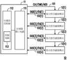
图1是根据本发明的范例实施例所示出的存储器存储装置的示意图。请参照图1,存储器存储装置10包括存储器控制电路单元11与易失性存储器模块12(1)~12(4)。须注意的是,易失性存储器模块12(1)~12(4)的总数可以是更多或更少,本发明不加以限制。FIG. 1 is a schematic diagram of a memory storage device according to an exemplary embodiment of the present invention. Referring to FIG. 1 , the
存储器控制电路单元11可用以控制并存取易失性存储器模块12(1)~12(4)。例如,存储器控制电路单元11可包括中央处理单元(Central Processing Unit,CPU)、或是其他可编程的一般用途或特殊用途的微处理器、数字信号处理器(Digital SignalProcessor,DSP)、可编程控制器、专用集成电路(Application Specific IntegratedCircuits,ASIC)、可编程逻辑器件(Programmable Logic Device,PLD)或其他类似装置或这些装置的组合。The memory
易失性存储器模块12(1)~12(4)可分别用以暂存数据。例如,易失性存储器模块12(1)~12(4)可分别包括第3代双通道同步动态随机存取存储器(Double Data Rate3SDRAM)、第4代双通道同步动态随机存取存储器(Double Data Rate 4SDRAM)、第5代双通道同步动态随机存取存储器(Double Data Rate 5 SDRAM)或其他类型的易失性存储器。存储器控制电路单元11可将数据存入易失性存储器模块12(1)~12(4)中或者从易失性存储器模块12(1)~12(4)中读取数据。The volatile memory modules 12(1)-12(4) are respectively used for temporarily storing data. For example, the volatile memory modules 12 ( 1 ) to 12 ( 4 ) may respectively include a third-generation dual-channel synchronous dynamic random access memory (Double Data Rate3SDRAM), a fourth-generation dual-channel synchronous dynamic random access memory (Double Data Rate3 Rate 4SDRAM), the fifth generation of dual-channel synchronous dynamic random access memory (Double Data Rate 5 SDRAM) or other types of volatile memory. The memory
存储器控制电路单元11可包括存储器接口电路111与存储器控制器112。存储器接口电路111并用以连接至易失性存储器模块12(1)~12(4)。例如,存储器接口电路111可通过外设部件互连局部总线(Peripheral Component Interconnect Express,PCI Express)标准或其他类型的连接接口标准与易失性存储器模块12(1)~12(4)通信。The memory
存储器控制器112连接至存储器接口电路111。存储器控制器112可通过存储器接口电路111对易失性存储器模块12(1)~12(4)执行存取操作。例如,所述存取操作可包括数据读取操作与数据写入操作。数据读取操作用以从易失性存储器模块12(1)~12(4)读取数据。数据写入操作用以将数据写入(即存储)至易失性存储器模块12(1)~12(4)中。在一范例实施例中,存储器控制器112亦称为动态随机存取存储器控制器(SRAM controller)。此外,存储器控制器112可负责存储器控制电路单元11的整体或部分操作。The
存储器接口电路111可通过信号路径(亦称为第一信号路径)101以fly-by的方式连接至易失性存储器模块12(1)~12(4)。亦即,在信号路径101上传输的信号会共用通道而依序抵达易失性存储器模块12(1)~12(4)。此外,存储器接口电路111可通过信号路径(亦称为第二信号路径)102(1)~102(4)平行连接至易失性存储器模块12(1)~12(4)。亦即,在信号路径102(1)~102(4)上传输的信号可通过各自独立的通道于存储器控制电路单元11与易失性存储器模块12(1)~12(4)之间传输。然而,信号路径101及102(1)~102(4)的设置方式亦可根据实务需求调整,本发明不加以限制。The
须注意的是,信号路径101为信号的单向传输路径。亦即,存储器控制电路单元11可通过信号路径101向易失性存储器模块12(1)~12(4)传送信号。信号路径102(1)~102(4)皆为信号的双向传输路径。例如,在写入数据至易失性存储器模块12(i)时,存储器控制电路单元11可通过信号路径102(i)向易失性存储器模块12(i)传送信号。或者,在从易失性存储器模块12(i)读取数据时,存储器控制电路单元11可通过信号路径102(i)接收来自易失性存储器模块12(i)的信号。It should be noted that the
信号路径101可用以传输信号(亦称为时钟信号)CLK至易失性存储器模块12(1)~12(4)。信号CLK可用以将存储器控制电路单元11的时钟(亦称为系统时钟)同步至易失性存储器模块12(1)~12(4)。此外,信号路径101亦可用以传输信号(亦称为指令信号)CMD与信号(亦称为地址信号)ADD至易失性存储器模块12(1)~12(4)。信号CMD可用以将存储器控制器112所欲执行的存取指令的信息传送给易失性存储器模块12(1)~12(4)。信号ADD可用以将存储器控制器112所欲存取的存储器地址的信息传送给易失性存储器模块12(1)~12(4)。此外,信号路径101亦可用以传输其他类型的信号,本发明不加以限制。The
信号路径102(1)~102(4)可分别用以传输信号(亦称为数据触发信号)DQS(1)~DQS(4)至易失性存储器模块12(1)~12(4)。此外,信号路径102(1)~102(4)亦可分别用以传输信号(亦称为数据信号)DQ(1)~DQ(4)至易失性存储器模块12(1)~12(4)。其中,信号DQS(i)与DQ(i)相互匹配。例如,信号DQS(i)可用以取样信号DQ(i),以获得信号DQ(i)所携带的数据。The signal paths 102(1)-102(4) are respectively used to transmit signals (also referred to as data trigger signals) DQS(1)-DQS(4) to the volatile memory modules 12(1)-12(4). In addition, the signal paths 102(1)-102(4) can also be used to transmit signals (also referred to as data signals) DQ(1)-DQ(4) to the volatile memory modules 12(1)-12(4) respectively. ). Wherein, signals DQS(i) and DQ(i) match each other. For example, the signal DQS(i) can be used to sample the signal DQ(i) to obtain the data carried by the signal DQ(i).
以信号路径102(i)为例,当欲将数据存储至易失性存储器模块12(i)时,存储器接口电路111可通过信号路径101将信号CLK、CMD及ADD传输至易失性存储器模块12(i)并通过信号路径102(i)将信号DQS(i)与DQ(i)传送至易失性存储器模块12(i)。根据通过信号路径101与102接收的信号,易失性存储器模块12(i)可执行相对应的数据写入操作。此数据写入操作可用以将存储器控制器112所欲存储的数据存储于易失性存储器模块12(i)中。特别是,在数据写入操作中,易失性存储器模块12(i)可使用信号DQS(i)来取样信号DQ(i),以获得存储器控制器112所欲存储的数据。Taking the signal path 102(i) as an example, when data is to be stored in the volatile memory module 12(i), the
另一方面,当欲从易失性存储器模块12(i)读取数据时,存储器接口电路111可通过信号路径101传输信号CLK、CMD及ADD至易失性存储器模块12(i)。根据通过信号路径101接收的信号,易失性存储器模块12(i)可执行相对应的数据读取操作。此数据读取操作可用以将存储器控制器112所欲读取的数据从易失性存储器模块12(i)中读取出来。然后,易失性存储器模块12(i)可通过信号路径102(i)将信号DQS(i)与DQ(i)传送至存储器接口电路111。存储器接口电路111可使用信号DQS(i)来取样信号DQ(i),以获得存储器控制器112所欲读取的数据。On the other hand, when data is to be read from the volatile memory module 12(i), the
在一范例实施例中,存储器接口电路111可根据内部的信号(亦称为内部时钟信号)产生信号CLK与信号DQS(i)。存储器接口电路111可将信号CLK与DQS(i)分别通过信号路径101与信号路径102(i)传送至易失性存储器模块(亦称为目标易失性存储器模块)12(i)。In an exemplary embodiment, the
在一范例实施例中,存储器控制电路单元11还包括控制电路(亦称为偏移控制电路)113。控制电路113可连接至存储器接口电路111。例如,控制电路113可设置于存储器控制器112中(如图1所示)、设置于存储器接口电路111中、或者独立于存储器接口电路111与存储器控制器112之外。例如,控制电路113可包括微处理器、嵌入式控制器(EmbeddedController,EC)或其他类似装置。在一范例实施例中,控制电路113亦可通过软件或固件的方式实施,本发明不加以限制。In an exemplary embodiment, the memory
控制电路113可获得信号DQS(i)于易失性存储器模块12(i)端与信号CLK之间的偏移量。例如,此偏移量可反映信号DQS(i)于易失性存储器模块12(i)端与信号CLK之间的相位差或频率差。须注意的是,关于如何获得信号DQS(i)于易失性存储器模块12(i)端与信号CLK之间的偏移量属于现有技术,例如可于易失性存储器模块12(i)端通过高频信号来对信号DQS(i)和/或CLK进行取样,以获得信号DQS(i)与CLK各自的转态点位置等,在此不多加赘述。The
控制电路113可判断此偏移量是否大于临界值。响应于此偏移量大于所述临界值,控制电路113可根据信号DQS(i)的延迟信息来存储(例如更新)信号DQS(i)的初始延迟设定。例如,信号DQS(i)的延迟信息可反映当前信号DQS(i)的延迟状态。尔后,存储器接口电路111可根据此初始延迟设定来重新产生具有相同延迟状态的信号DQS(i)。另一方面,响应于此偏移量不大于(例如小于或等于)所述临界值,控制电路113可舍弃(即不存储)信号DQS(i)的延迟信息。The
在一范例实施例中,在存储所述初始延迟设定后,存储器接口电路111可根据内部时钟信号与所述初始延迟设定重新产生信号DQS(i)。须注意的是,所述初始延迟设定是根据于易失性存储器模块12(i)端与信号CLK之间的偏移量大于临界值的信号DQS(i)而存储,故重新产生的信号DQS(i)于易失性存储器模块12(i)端与信号CLK之间的偏移量理论上也会大于所述临界值。存储器接口电路111可根据重新产生的信号DQS(i)来调整信号的延迟量,以将信号DQS(i)于易失性存储器模块12(i)端与信号CLK对齐。例如,所述对齐可以是指信号DQS(i)的上升缘与信号CLK的上升缘相互对齐、信号DQS(i)的下降缘与信号CLK的下降缘相互对齐或者其他的对齐方式,视实务需求而定。在一范例实施例中,存储器接口电路111根据重新产生的信号DQS(i)来调整信号的延迟量,以将信号DQS(i)于易失性存储器模块12(i)端与信号CLK对齐的操作,亦可称为写入均衡(write leveling)。须注意的是,写入均衡属于相关技术领域的现有技术,故在此不多加赘述。In an exemplary embodiment, after storing the initial delay setting, the
在一范例实施例中,通过使用所述初始延迟设定来产生执行写入均衡的信号DQS(i),可确保在写入均衡的初始阶段,信号DQS(i)于易失性存储器模块12(i)端与信号CLK之间的偏差值大于(或不小于)所述临界值。由此,在执行写入均衡而锁定信号CLK与DQS(i)后,可减少锁定后的信号CLK与DQS(i)之间发生时序错乱(例如将信号CLK中的第T(0)个脉冲锁定至信号DQS(i)中的第T(1)个脉冲)的机率。In an exemplary embodiment, by using the initial delay setting to generate the signal DQS(i) for performing write leveling, it can be ensured that the signal DQS(i) is in the
在一范例实施例中,存储器接口电路111可检测开机信号。例如,此开机信号可于存储器存储装置10每次开机或上电时自动产生。存储器接口电路111可响应于此开机信号而根据内部时钟信号与所述初始延迟设定产生信号DQS(i)。然后,存储器接口电路111可基于根据所述初始延迟设定产生的信号DQS(i),于易失性存储器模块12(i)端执行写入均衡,以使信号DQS(i)于易失性存储器模块12(i)端与信号CLK对齐。In an exemplary embodiment, the
在一范例实施例中,控制电路113可获得信号DQS(i)于易失性存储器模块12(i)端与信号CLK之间的多个偏移量(亦称为候选偏移量)。每一个候选偏移量可能受不同时间点通道中的噪声(noise)或抖动(jitter)影响而有所不同。存储器控制器112可对此些候选偏移量进行统计运算,以获得最终要用来与临界值进行比对的偏移量。由此,可针对当前采用的信号DQS(i)取得较为客观且对于误差的容许度较高的偏移量的统计数据,进而根据此统计数据来决定是否根据此信号DQS(i)的延迟信息来存储所述初始延迟设定。相关细节已详述于上,在此不重复赘述。In an exemplary embodiment, the
图2是根据本发明的范例实施例所示出的时钟信号与数据触发信号于易失性存储器模块端的信号时序示意图。请参照图1与图2,假设信号DQS(i)包括信号DQS_SEL(1)~DQS_SEL(4)。信号CLK与DQS_SEL(1)~DQS_SEL(4)皆可根据内部时钟信号而产生。特别是,信号DQS_SEL(1)~DQS_SEL(4)的相位各不相同。此外,信号DQS_SEL(1)~DQS_SEL(4)的总数可以是更多或更少,本发明不加以限制。FIG. 2 is a schematic diagram showing the signal timing of the clock signal and the data trigger signal at the volatile memory module end according to an exemplary embodiment of the present invention. Referring to FIG. 1 and FIG. 2 , it is assumed that the signal DQS(i) includes signals DQS_SEL( 1 )˜DQS_SEL( 4 ). The signals CLK and DQS_SEL( 1 )˜DQS_SEL( 4 ) can all be generated according to the internal clock signal. In particular, the phases of the signals DQS_SEL( 1 )˜DQS_SEL( 4 ) are different. In addition, the total number of signals DQS_SEL( 1 )˜DQS_SEL( 4 ) may be more or less, which is not limited by the present invention.
在一范例实施例中,存储器接口电路111可将信号DQS_SEL(1)~DQS_SEL(4)的其中之一的延迟量增加m个延迟时间单位以产生信号DQS_SEL(1)~DQS_SEL(4)的其中之另一。所述延迟时间单位可对应信号DQS(i)的一个时钟周期的1/n,其中m与n皆为正整数。例如,假设n为4,则存储器接口电路111可将信号DQS_SEL(1)的延迟量增加1至3个延迟时间单位以分别产生信号DQS_SEL(2)~DQS_SEL(4)。信号DQS_SEL(1)~DQS_SEL(4)彼此间的相位可各相差90度(对应于1/4个时钟周期)或其他度数。In an exemplary embodiment, the
在一范例实施例中,存储器接口电路111可将信号DQS_SEL(1)~DQS_SEL(4)的其中之一传送至易失性存储器模块12(i)。存储器控制器112可判断信号DQS_SEL(1)~DQS_SEL(4)的其中之一于易失性存储器模块12(i)端与信号CLK之间的偏移量是否大于临界值。响应于信号DQS_SEL(1)~DQS_SEL(4)的其中之一(例如信号DQS_SEL(j))于易失性存储器模块12(i)端与信号CLK之间的偏移量(亦称为第一偏移量)不大于临界值,存储器控制器112可舍弃(即不存储)信号DQS_SEL(j)的延迟信息。例如,信号DQS_SEL(j)的延迟信息可反映信号DQS_SEL(j)的延迟状态。或者,响应于信号DQS_SEL(1)~DQS_SEL(4)的其中之一(例如信号DQS_SEL(k))于易失性存储器模块12(i)端与信号CLK之间的偏移量(亦称为第二偏移量)大于临界值,则存储器控制器112可存储信号DQS_SEL(k)的延迟信息作为信号DQS(i)的初始延迟设定。例如,信号DQS_SEL(k)的延迟信息可反映信号DQS_SEL(k)的延迟状态。k不同于j。In an exemplary embodiment, the
以图2为例,信号DQS_SEL(j)可包括信号DQS_SEL(1)与DQS_SEL(2)。例如,信号DQS_SEL(1)与DQS_SEL(2)的上升缘皆位于过滤区域GP内。例如,过滤区域GP两端的边界201与202是以信号CLK的上升缘为中心进行界定。例如,以信号CLK的上升缘分别向左与向右延伸一个时间单位,可获得过滤区域GP两端的边界201与202。须注意的是,过滤区域GP的宽度(即边界201与202之间的距离)亦可根据实务需求调整,本发明不加以限制。Taking FIG. 2 as an example, the signal DQS_SEL(j) may include signals DQS_SEL(1) and DQS_SEL(2). For example, the rising edges of the signals DQS_SEL( 1 ) and DQS_SEL( 2 ) are both located in the filter region GP. For example, the
在一范例实施例中,信号DQS_SEL(j)的上升缘位于过滤区域GP内,表示信号DQS_SEL(j)的边界(boundary)相对接近信号CLK的边界。因此,后续若使用信号DQS_SEL(j)作为信号DQS(i)来与信号CLK执行写入均衡(即相位校正),则锁定后的信号CLK与DQS(i)之间容易发生时序错乱。在一范例实施例中,通过将信号DQS_SEL(j)排除,可减少锁定后的信号CLK与DQS(i)之间发生时序错乱的机率。In an exemplary embodiment, the rising edge of the signal DQS_SEL(j) is located within the filtering region GP, which means that the boundary of the signal DQS_SEL(j) is relatively close to the boundary of the signal CLK. Therefore, if the signal DQS_SEL(j) is subsequently used as the signal DQS(i) to perform write equalization (ie, phase correction) with the signal CLK, timing disorder is likely to occur between the locked signal CLK and DQS(i). In an exemplary embodiment, by excluding the signal DQS_SEL(j), the probability of timing disorder between the locked signal CLK and DQS(i) can be reduced.
在一范例实施例中,信号DQS_SEL(k)可包括信号DQS_SEL(3)与DQS_SEL(4)。例如,DQS_SEL(3)与DQS_SEL(4)的上升缘皆非位于过滤区域GP内。In an exemplary embodiment, the signal DQS_SEL(k) may include signals DQS_SEL( 3 ) and DQS_SEL( 4 ). For example, the rising edges of DQS_SEL(3) and DQS_SEL(4) are not located in the filter region GP.
在一范例实施例中,信号DQS_SEL(k)的上升缘非位于过滤区域GP内,表示信号DQS_SEL(k)的边界相对远离信号CLK的边界。因此,后续若使用信号DQS_SEL(k)作为信号DQS(i)来与信号CLK执行写入均衡,则锁定后的信号CLK与DQS(i)之间发生时序错乱的机率可被降低。在一范例实施例中,选用信号DQS_SEL(k)作为信号DQS(i)来执行写入均衡,可减少锁定后的信号CLK与DQS(i)之间发生时序错乱的机率。In an exemplary embodiment, the rising edge of the signal DQS_SEL(k) is not located in the filter region GP, which means that the boundary of the signal DQS_SEL(k) is relatively far from the boundary of the signal CLK. Therefore, if the signal DQS_SEL(k) is subsequently used as the signal DQS(i) to perform write equalization with the signal CLK, the probability of timing disorder between the locked signal CLK and DQS(i) can be reduced. In an exemplary embodiment, the signal DQS_SEL(k) is selected as the signal DQS(i) to perform write equalization, which can reduce the probability of timing disorder between the locked signal CLK and DQS(i).
在一范例实施例中,存储器接口电路111可先将信号DQS_SEL(j)传送至易失性存储器模块12(i)。在判定第一偏移量不大于所述临界值后,存储器接口电路111可产生信号DQS_SEL(k)并将信号DQS_SEL(k)传送至易失性存储器模块12(i),依此类推,直到找到合适的信号DQS_SEL(k)为止。In an exemplary embodiment, the
图3是根据本发明的范例实施例所示出的存储器控制电路单元的示意图。请参照图3,存储器控制电路单元31可相同或相似与图1的存储器控制电路单元11。存储器控制电路单元31可包括存储器接口电路311、存储器控制器312及控制电路313。存储器接口电路311、存储器控制器312及控制电路313可分别相同或相似于图1的存储器接口电路111、存储器控制器112及控制电路113。FIG. 3 is a schematic diagram of a memory control circuit unit according to an exemplary embodiment of the present invention. Referring to FIG. 3 , the memory
存储器接口电路311可包括内部时钟产生器32、时钟路径(clock path)电路33、暂存器34及写入路径(write path)电路35。内部时钟产生器32连接至时钟路径电路33与写入路径电路35。暂存器34连接至写入路径电路35。此外,存储器接口电路311中还可具有诸如读取路径(read path)电路及复用器等各式电子电路元件,本发明不加以限制。The
内部时钟产生器32可用以产生信号(即内部时钟信号)ICK。时钟路径电路33可根据信号ICK产生信号CLK。信号CLK可被传送至易失性存储器模块12(i)。暂存器34可用以存储信号DQS(i)的初始延迟设定。写入路径电路35可根据信号ICK与暂存器34中的初始延迟设定产生具有特定延迟状态的信号DQS(i)。然后,信号DQS(i)可被传送至易失性存储器模块12(i)。尔后,于易失性存储器模块12(i)端的写入均衡可根据此信号DQS(i)执行。相关细节皆已详述于上,在此不多加赘述。The
图4是根据本发明的范例实施例所示出的存储器存储装置的示意图。请参照图4,存储器存储装置40包括连接接口单元41、存储器控制电路单元42、可复写式非易失性存储器模块43及易失性存储器模块44。FIG. 4 is a schematic diagram of a memory storage device according to an exemplary embodiment of the present invention. Referring to FIG. 4 , the
连接接口单元41用以将存储器存储装置40连接主机系统11。存储器存储装置40可通过连接接口单元41与主机系统通信。在一范例实施例中,连接接口单元41是相容于PCIExpress标准。在一范例实施例中,连接接口单元41亦可以是符合串行高级技术附件(Serial Advanced Technology Attachment,SATA)标准、并行高级技术附件(ParallelAdvanced Technology Attachment,PATA)标准、电气和电子工程师协会(Institute ofElectrical and Electronic Engineers,IEEE)1394标准、通用串行总线(UniversalSerial Bus,USB)标准、SD接口标准、超高速一代(Ultra High Speed-I,UHS-I)接口标准、超高速二代(Ultra High Speed-II,UHS-II)接口标准、存储棒(Memory Stick,MS)接口标准、MCP接口标准、MMC接口标准、eMMC接口标准、通用快闪存储器(Universal FlashStorage,UFS)接口标准、eMCP接口标准、CF接口标准、整合式驱动电子接口(IntegratedDevice Electronics,IDE)标准或其他适合的标准。连接接口单元41可与存储器控制电路单元42封装在一个芯片中,或者连接接口单元41是布设于一包含存储器控制电路单元42的芯片外。The
存储器控制电路单元42连接至连接接口单元41、可复写式非易失性存储器模块43及易失性存储器模块44。存储器控制电路单元42用以执行以硬件型式或固件型式实作的多个逻辑门或控制指令并且根据主机系统的指令在可复写式非易失性存储器模块43中进行数据的写入、读取与抹除等运作。此外,存储器控制电路单元42可包括图1的存储器控制电路单元11或图3的存储器控制电路单元31。The memory
可复写式非易失性存储器模块43用以存储主机系统所写入的数据。例如,可复写式非易失性存储器模块43可包括单阶存储单元(Single Level Cell,SLC)NAND型快闪存储器模块(即,一个存储单元中可存储1个比特的快闪存储器模块)、二阶存储单元(MultiLevel Cell,MLC)NAND型快闪存储器模块(即,一个存储单元中可存储2个比特的快闪存储器模块)、三阶存储单元(Triple Level Cell,TLC)NAND型快闪存储器模块(即,一个存储单元中可存储3个比特的快闪存储器模块)、四阶存储单元(Quad Level Cell,QLC)NAND型快闪存储器模块(即,一个存储单元中可存储4个比特的快闪存储器模块)、其他快闪存储器模块或其他具有相同特性的存储器模块。The rewritable
可复写式非易失性存储器模块43中的每一个存储单元是以电压(以下亦称为临界电压)的改变来存储一或多个比特。具体来说,每一个存储单元的控制门(control gate)与通道之间有一个电荷捕捉层。通过施予一写入电压至控制门,可以改变电荷补捉层的电子量,进而改变存储单元的临界电压。此改变存储单元的临界电压的操作亦称为“把数据写入至存储单元”或“程序化(programming)存储单元”。随着临界电压的改变,可复写式非易失性存储器模块43中的每一个存储单元具有多个存储状态。通过施予读取电压可以判断一个存储单元是属于哪一个存储状态,由此取得此存储单元所存储的一或多个比特。Each memory cell in the rewritable
在一范例实施例中,可复写式非易失性存储器模块43的存储单元可构成多个实体程序化单元,并且此些实体程序化单元可构成多个实体抹除单元。具体来说,同一条字线上的存储单元可组成一或多个实体程序化单元。若一个存储单元可存储2个以上的比特,则同一条字线上的实体程序化单元可至少可被分类为下实体程序化单元与上实体程序化单元。例如,一存储单元的最低有效比特(Least Significant Bit,LSB)是属于下实体程序化单元,并且一存储单元的最高有效比特(Most Significant Bit,MSB)是属于上实体程序化单元。一般来说,在MLC NAND型快闪存储器中,下实体程序化单元的写入速度会大于上实体程序化单元的写入速度,和/或下实体程序化单元的可靠度是高于上实体程序化单元的可靠度。In an exemplary embodiment, the storage units of the rewritable
在一范例实施例中,实体程序化单元为程序化的最小单元。即,实体程序化单元为写入数据的最小单元。例如,实体程序化单元可为实体页(page)或是实体扇(sector)。若实体程序化单元为实体页,则此些实体程序化单元可包括数据比特区与冗余(redundancy)比特区。数据比特区包含多个实体扇,用以存储用户数据,而冗余比特区用以存储系统数据(例如,错误更正码等管理数据)。在一范例实施例中,数据比特区包含32个实体扇,且一个实体扇的大小为512字节(byte,B)。然而,在其他范例实施例中,数据比特区中也可包含8个、16个或数目更多或更少的实体扇,并且每一个实体扇的大小也可以是更大或更小。另一方面,实体抹除单元为抹除的最小单位。亦即,每一实体抹除单元含有最小数目的一并被抹除的存储单元。例如,实体抹除单元为实体区块(block)。In an exemplary embodiment, the entity programming unit is the smallest unit of programming. That is, the entity programming unit is the smallest unit for writing data. For example, the physical programming unit may be a physical page or a physical sector. If the physical programming units are physical pages, these physical programming units may include data bit areas and redundancy (redundancy) bit areas. The data bit area includes a plurality of physical sectors for storing user data, and the redundant bit area is used for storing system data (eg, management data such as error correction codes). In an exemplary embodiment, the data bit area includes 32 physical sectors, and the size of one physical sector is 512 bytes (byte, B). However, in other exemplary embodiments, the data bit area may also include 8, 16 or more or less physical sectors, and the size of each physical sector may also be larger or smaller. On the other hand, the entity erasing unit is the smallest unit of erasing. That is, each physical erase unit contains the minimum number of memory cells to be erased together. For example, the physical erasing unit is a physical block.
易失性存储器模块44用以易失性地存储数据。例如,易失性存储器模块44可包括图1的易失性存储器模块12(1)~12(4)。此外,易失性存储器模块44的总数可以是更多或更少。The
图5是根据本发明的范例实施例所示出的信号校正方法的流程图。请参照图5,在步骤S501中,根据内部时钟信号产生时钟信号与数据触发信号。在步骤S502中,将所述时钟信号与所述数据触发信号分别通过第一信号路径与第二信号路径传送至多个易失性存储器模块中的目标易失性存储器模块。在步骤S503中,获得所述数据触发信号于所述目标易失性存储器模块端与所述时钟信号之间的偏移量。在步骤S504中,响应于所述偏移量大于临界值,根据所述数据触发信号的延迟信息存储所述数据触发信号的初始延迟设定。Fig. 5 is a flowchart of a signal correction method according to an exemplary embodiment of the present invention. Referring to FIG. 5 , in step S501 , a clock signal and a data trigger signal are generated according to an internal clock signal. In step S502, the clock signal and the data trigger signal are respectively transmitted to a target volatile memory module among the plurality of volatile memory modules through a first signal path and a second signal path. In step S503, an offset between the data trigger signal at the target volatile memory module end and the clock signal is obtained. In step S504, in response to the offset being greater than a critical value, storing the initial delay setting of the data trigger signal according to the delay information of the data trigger signal.
图6是根据本发明的范例实施例所示出的信号校正方法的流程图。请参照图6,在步骤S601中,存储器存储装置上电(例如开机或唤醒)。在步骤S602中,根据内部时钟信号与初始延迟设定产生数据触发信号。在步骤S603中,根据所述时钟信号调整所述数据触发信号的延迟量,以将所述数据触发信号于所述目标易失性存储器模块端与所述时钟信号对齐。Fig. 6 is a flowchart of a signal correction method according to an exemplary embodiment of the present invention. Referring to FIG. 6 , in step S601 , the memory storage device is powered on (for example, turned on or woken up). In step S602, a data trigger signal is generated according to an internal clock signal and an initial delay setting. In step S603, the delay amount of the data trigger signal is adjusted according to the clock signal, so as to align the data trigger signal at the target volatile memory module end with the clock signal.
然而,图5与图6中各步骤已详细说明如上,在此便不再赘述。值得注意的是,图5与图6中各步骤可以实作为多个程序码或是电路,本案不加以限制。此外,图5与图6的方法可以搭配以上范例实施例使用,也可以单独使用,本案不加以限制。However, each step in FIG. 5 and FIG. 6 has been described in detail above, and will not be repeated here. It should be noted that each step in FIG. 5 and FIG. 6 can be implemented as a plurality of program codes or circuits, which is not limited in this case. In addition, the methods shown in FIG. 5 and FIG. 6 can be used together with the above exemplary embodiments, or can be used alone, which is not limited in this case.
综上所述,本发明实施例提供的信号校准方法、存储器存储装置及存储器控制电路单元,可针对不同的易失性存储器模块来存储数据触发信号的初始延迟设定。特别是,根据所述初始延迟设定所产生的数据触发信号在易失性存储器端与时钟信号之间的偏移量会大于临界值。由此,在对数据触发信号执行写入均衡后,可减少锁定后的时钟信号与数据触发信号之间发生时序错乱的机率。To sum up, the signal calibration method, the memory storage device and the memory control circuit unit provided by the embodiments of the present invention can store the initial delay setting of the data trigger signal for different volatile memory modules. In particular, the offset between the volatile memory terminal and the clock signal of the data trigger signal generated according to the initial delay setting will be greater than a threshold value. In this way, after performing write equalization on the data trigger signal, the probability of timing disorder between the locked clock signal and the data trigger signal can be reduced.
最后应说明的是:以上各实施例仅用以说明本发明的技术方案,而非对其限制;尽管参照前述各实施例对本发明进行了详细的说明,本领域的普通技术人员应当理解:其依然可以对前述各实施例所记载的技术方案进行修改,或者对其中部分或者全部技术特征进行等同替换;而这些修改或者替换,并不使相应技术方案的本质脱离本发明各实施例技术方案的范围。Finally, it should be noted that: the above embodiments are only used to illustrate the technical solutions of the present invention, rather than limiting them; although the present invention has been described in detail with reference to the foregoing embodiments, those of ordinary skill in the art should understand that: It is still possible to modify the technical solutions described in the foregoing embodiments, or perform equivalent replacements for some or all of the technical features; and these modifications or replacements do not make the essence of the corresponding technical solutions deviate from the technical solutions of the various embodiments of the present invention. scope.
Claims (21)
Priority Applications (2)
| Application Number | Priority Date | Filing Date | Title |
|---|---|---|---|
| CN202211211298.1ACN115565572A (en) | 2022-09-30 | 2022-09-30 | Signal calibration method, memory storage device and memory control circuit unit |
| US17/983,407US12008242B2 (en) | 2022-09-30 | 2022-11-09 | Signal calibration method, memory storage device, and memory control circuit unit |
Applications Claiming Priority (1)
| Application Number | Priority Date | Filing Date | Title |
|---|---|---|---|
| CN202211211298.1ACN115565572A (en) | 2022-09-30 | 2022-09-30 | Signal calibration method, memory storage device and memory control circuit unit |
Publications (1)
| Publication Number | Publication Date |
|---|---|
| CN115565572Atrue CN115565572A (en) | 2023-01-03 |
Family
ID=84742519
Family Applications (1)
| Application Number | Title | Priority Date | Filing Date |
|---|---|---|---|
| CN202211211298.1APendingCN115565572A (en) | 2022-09-30 | 2022-09-30 | Signal calibration method, memory storage device and memory control circuit unit |
Country Status (2)
| Country | Link |
|---|---|
| US (1) | US12008242B2 (en) |
| CN (1) | CN115565572A (en) |
Cited By (1)
| Publication number | Priority date | Publication date | Assignee | Title |
|---|---|---|---|---|
| CN116863980A (en)* | 2023-07-24 | 2023-10-10 | 上海奎芯集成电路设计有限公司 | Dynamic adjusting circuit and method for gating signals |
Citations (7)
| Publication number | Priority date | Publication date | Assignee | Title |
|---|---|---|---|---|
| US20050047192A1 (en)* | 2003-09-03 | 2005-03-03 | Renesas Technology Corp. | Semiconductor integrated circuit |
| JP2013008112A (en)* | 2011-06-22 | 2013-01-10 | Panasonic Corp | Memory controller and delay adjustment method |
| CN102981781A (en)* | 2012-10-15 | 2013-03-20 | 威盛电子股份有限公司 | Data storage device, storage medium controller and control method |
| CN104012002A (en)* | 2011-12-29 | 2014-08-27 | 瑞萨电子株式会社 | Semiconductor device |
| US9659618B1 (en)* | 2016-06-08 | 2017-05-23 | Phison Electronics Corp. | Memory interface, memory control circuit unit, memory storage device and clock generation method |
| CN114141284A (en)* | 2020-09-04 | 2022-03-04 | 美光科技公司 | Access Command Delay Using Delay Locked Loop (DLL) Circuitry |
| CN115114198A (en)* | 2022-04-20 | 2022-09-27 | 腾讯科技(深圳)有限公司 | Signal delay control method, device, device and medium |
Family Cites Families (1)
| Publication number | Priority date | Publication date | Assignee | Title |
|---|---|---|---|---|
| US7301831B2 (en)* | 2004-09-15 | 2007-11-27 | Rambus Inc. | Memory systems with variable delays for write data signals |
- 2022
- 2022-09-30CNCN202211211298.1Apatent/CN115565572A/enactivePending
- 2022-11-09USUS17/983,407patent/US12008242B2/enactiveActive
Patent Citations (7)
| Publication number | Priority date | Publication date | Assignee | Title |
|---|---|---|---|---|
| US20050047192A1 (en)* | 2003-09-03 | 2005-03-03 | Renesas Technology Corp. | Semiconductor integrated circuit |
| JP2013008112A (en)* | 2011-06-22 | 2013-01-10 | Panasonic Corp | Memory controller and delay adjustment method |
| CN104012002A (en)* | 2011-12-29 | 2014-08-27 | 瑞萨电子株式会社 | Semiconductor device |
| CN102981781A (en)* | 2012-10-15 | 2013-03-20 | 威盛电子股份有限公司 | Data storage device, storage medium controller and control method |
| US9659618B1 (en)* | 2016-06-08 | 2017-05-23 | Phison Electronics Corp. | Memory interface, memory control circuit unit, memory storage device and clock generation method |
| CN114141284A (en)* | 2020-09-04 | 2022-03-04 | 美光科技公司 | Access Command Delay Using Delay Locked Loop (DLL) Circuitry |
| CN115114198A (en)* | 2022-04-20 | 2022-09-27 | 腾讯科技(深圳)有限公司 | Signal delay control method, device, device and medium |
Cited By (2)
| Publication number | Priority date | Publication date | Assignee | Title |
|---|---|---|---|---|
| CN116863980A (en)* | 2023-07-24 | 2023-10-10 | 上海奎芯集成电路设计有限公司 | Dynamic adjusting circuit and method for gating signals |
| CN116863980B (en)* | 2023-07-24 | 2024-01-26 | 上海奎芯集成电路设计有限公司 | Dynamic adjusting circuit and method for gating signals |
Also Published As
| Publication number | Publication date |
|---|---|
| US20240111430A1 (en) | 2024-04-04 |
| US12008242B2 (en) | 2024-06-11 |
Similar Documents
| Publication | Publication Date | Title |
|---|---|---|
| US11164634B2 (en) | Non-volatile storage system with fast SLC operation | |
| US10635131B2 (en) | Interface adjustment processes for a data storage device | |
| TW201907287A (en) | Data reading method and storage controller | |
| US11036582B2 (en) | Uncorrectable error correction code (UECC) recovery time improvement | |
| CN104636267B (en) | Memory control method, memory storage device and memory control circuit unit | |
| US20200252072A1 (en) | Clock and data recovery circuit, memory storage device and flash memory controller | |
| US20230368825A1 (en) | Storage controller, storage device, and operation method of storage device | |
| US10749728B1 (en) | Signal calibration circuit, memory storage device and signal calibration method | |
| CN115565572A (en) | Signal calibration method, memory storage device and memory control circuit unit | |
| US11206157B1 (en) | Signal receiving circuit, memory storage device and calibration method of equalizer circuit | |
| CN104167220B (en) | Data reading method, control circuit, memory module and memory storage device | |
| CN107545918B (en) | Memory control circuit unit, storage device and reference voltage generation method | |
| CN113419683B (en) | Memory access method, memory storage device and memory control circuit unit | |
| TWI857357B (en) | Signal calibration method, memory storage device and memory control circuit unit | |
| CN116052746A (en) | Voltage correction method, memory storage device and memory control circuit unit | |
| TWI727656B (en) | Clock and data recovery circuit, memory storage device and signal adjustment method | |
| CN111610937A (en) | Data writing method, memory storage device and memory control circuit unit | |
| CN111585547B (en) | Signal correction circuit, memory storage device and signal correction method | |
| CN113284527B (en) | Clock data recovery circuit, memory storage device and signal adjustment method | |
| CN112447210B (en) | Connection interface circuit, memory storage device and signal generation method | |
| TWI600017B (en) | Memory control circuit unit, memory storage device and reference voltage generation method | |
| CN111654266B (en) | Clock data recovery circuit, memory storage device and flash memory controller | |
| US12292825B2 (en) | Memory control method, memory storage device and memory control circuit unit | |
| CN114610236B (en) | Memory control method, memory storage device and memory control circuit unit | |
| CN113450843B (en) | Circuit layout structure and memory storage device |
Legal Events
| Date | Code | Title | Description |
|---|---|---|---|
| PB01 | Publication | ||
| PB01 | Publication | ||
| SE01 | Entry into force of request for substantive examination | ||
| SE01 | Entry into force of request for substantive examination |