CN115561938B - Array substrate, display panel and display device - Google Patents
Array substrate, display panel and display deviceDownload PDFInfo
- Publication number
- CN115561938B CN115561938BCN202211545695.2ACN202211545695ACN115561938BCN 115561938 BCN115561938 BCN 115561938BCN 202211545695 ACN202211545695 ACN 202211545695ACN 115561938 BCN115561938 BCN 115561938B
- Authority
- CN
- China
- Prior art keywords
- display panel
- substrate
- electrode
- pixel
- sub
- Prior art date
- Legal status (The legal status is an assumption and is not a legal conclusion. Google has not performed a legal analysis and makes no representation as to the accuracy of the status listed.)
- Active
Links
Images


Classifications
- G—PHYSICS
- G02—OPTICS
- G02F—OPTICAL DEVICES OR ARRANGEMENTS FOR THE CONTROL OF LIGHT BY MODIFICATION OF THE OPTICAL PROPERTIES OF THE MEDIA OF THE ELEMENTS INVOLVED THEREIN; NON-LINEAR OPTICS; FREQUENCY-CHANGING OF LIGHT; OPTICAL LOGIC ELEMENTS; OPTICAL ANALOGUE/DIGITAL CONVERTERS
- G02F1/00—Devices or arrangements for the control of the intensity, colour, phase, polarisation or direction of light arriving from an independent light source, e.g. switching, gating or modulating; Non-linear optics
- G02F1/01—Devices or arrangements for the control of the intensity, colour, phase, polarisation or direction of light arriving from an independent light source, e.g. switching, gating or modulating; Non-linear optics for the control of the intensity, phase, polarisation or colour
- G02F1/13—Devices or arrangements for the control of the intensity, colour, phase, polarisation or direction of light arriving from an independent light source, e.g. switching, gating or modulating; Non-linear optics for the control of the intensity, phase, polarisation or colour based on liquid crystals, e.g. single liquid crystal display cells
- G02F1/133—Constructional arrangements; Operation of liquid crystal cells; Circuit arrangements
- G02F1/1333—Constructional arrangements; Manufacturing methods
- G02F1/1343—Electrodes
- G02F1/134309—Electrodes characterised by their geometrical arrangement
- G02F1/134345—Subdivided pixels, e.g. for grey scale or redundancy
- G—PHYSICS
- G02—OPTICS
- G02F—OPTICAL DEVICES OR ARRANGEMENTS FOR THE CONTROL OF LIGHT BY MODIFICATION OF THE OPTICAL PROPERTIES OF THE MEDIA OF THE ELEMENTS INVOLVED THEREIN; NON-LINEAR OPTICS; FREQUENCY-CHANGING OF LIGHT; OPTICAL LOGIC ELEMENTS; OPTICAL ANALOGUE/DIGITAL CONVERTERS
- G02F1/00—Devices or arrangements for the control of the intensity, colour, phase, polarisation or direction of light arriving from an independent light source, e.g. switching, gating or modulating; Non-linear optics
- G02F1/01—Devices or arrangements for the control of the intensity, colour, phase, polarisation or direction of light arriving from an independent light source, e.g. switching, gating or modulating; Non-linear optics for the control of the intensity, phase, polarisation or colour
- G02F1/13—Devices or arrangements for the control of the intensity, colour, phase, polarisation or direction of light arriving from an independent light source, e.g. switching, gating or modulating; Non-linear optics for the control of the intensity, phase, polarisation or colour based on liquid crystals, e.g. single liquid crystal display cells
- G02F1/133—Constructional arrangements; Operation of liquid crystal cells; Circuit arrangements
- G02F1/1333—Constructional arrangements; Manufacturing methods
- G02F1/1339—Gaskets; Spacers; Sealing of cells
- G02F1/13394—Gaskets; Spacers; Sealing of cells spacers regularly patterned on the cell subtrate, e.g. walls, pillars
- G—PHYSICS
- G02—OPTICS
- G02F—OPTICAL DEVICES OR ARRANGEMENTS FOR THE CONTROL OF LIGHT BY MODIFICATION OF THE OPTICAL PROPERTIES OF THE MEDIA OF THE ELEMENTS INVOLVED THEREIN; NON-LINEAR OPTICS; FREQUENCY-CHANGING OF LIGHT; OPTICAL LOGIC ELEMENTS; OPTICAL ANALOGUE/DIGITAL CONVERTERS
- G02F1/00—Devices or arrangements for the control of the intensity, colour, phase, polarisation or direction of light arriving from an independent light source, e.g. switching, gating or modulating; Non-linear optics
- G02F1/01—Devices or arrangements for the control of the intensity, colour, phase, polarisation or direction of light arriving from an independent light source, e.g. switching, gating or modulating; Non-linear optics for the control of the intensity, phase, polarisation or colour
- G02F1/13—Devices or arrangements for the control of the intensity, colour, phase, polarisation or direction of light arriving from an independent light source, e.g. switching, gating or modulating; Non-linear optics for the control of the intensity, phase, polarisation or colour based on liquid crystals, e.g. single liquid crystal display cells
- G02F1/133—Constructional arrangements; Operation of liquid crystal cells; Circuit arrangements
- G02F1/1333—Constructional arrangements; Manufacturing methods
- G02F1/1343—Electrodes
- G02F1/134309—Electrodes characterised by their geometrical arrangement
- G02F1/134318—Electrodes characterised by their geometrical arrangement having a patterned common electrode
- G—PHYSICS
- G02—OPTICS
- G02F—OPTICAL DEVICES OR ARRANGEMENTS FOR THE CONTROL OF LIGHT BY MODIFICATION OF THE OPTICAL PROPERTIES OF THE MEDIA OF THE ELEMENTS INVOLVED THEREIN; NON-LINEAR OPTICS; FREQUENCY-CHANGING OF LIGHT; OPTICAL LOGIC ELEMENTS; OPTICAL ANALOGUE/DIGITAL CONVERTERS
- G02F1/00—Devices or arrangements for the control of the intensity, colour, phase, polarisation or direction of light arriving from an independent light source, e.g. switching, gating or modulating; Non-linear optics
- G02F1/01—Devices or arrangements for the control of the intensity, colour, phase, polarisation or direction of light arriving from an independent light source, e.g. switching, gating or modulating; Non-linear optics for the control of the intensity, phase, polarisation or colour
- G02F1/13—Devices or arrangements for the control of the intensity, colour, phase, polarisation or direction of light arriving from an independent light source, e.g. switching, gating or modulating; Non-linear optics for the control of the intensity, phase, polarisation or colour based on liquid crystals, e.g. single liquid crystal display cells
- G02F1/133—Constructional arrangements; Operation of liquid crystal cells; Circuit arrangements
- G02F1/136—Liquid crystal cells structurally associated with a semi-conducting layer or substrate, e.g. cells forming part of an integrated circuit
- G02F1/1362—Active matrix addressed cells
- G02F1/136213—Storage capacitors associated with the pixel electrode
- G—PHYSICS
- G02—OPTICS
- G02F—OPTICAL DEVICES OR ARRANGEMENTS FOR THE CONTROL OF LIGHT BY MODIFICATION OF THE OPTICAL PROPERTIES OF THE MEDIA OF THE ELEMENTS INVOLVED THEREIN; NON-LINEAR OPTICS; FREQUENCY-CHANGING OF LIGHT; OPTICAL LOGIC ELEMENTS; OPTICAL ANALOGUE/DIGITAL CONVERTERS
- G02F1/00—Devices or arrangements for the control of the intensity, colour, phase, polarisation or direction of light arriving from an independent light source, e.g. switching, gating or modulating; Non-linear optics
- G02F1/01—Devices or arrangements for the control of the intensity, colour, phase, polarisation or direction of light arriving from an independent light source, e.g. switching, gating or modulating; Non-linear optics for the control of the intensity, phase, polarisation or colour
- G02F1/13—Devices or arrangements for the control of the intensity, colour, phase, polarisation or direction of light arriving from an independent light source, e.g. switching, gating or modulating; Non-linear optics for the control of the intensity, phase, polarisation or colour based on liquid crystals, e.g. single liquid crystal display cells
- G02F1/133—Constructional arrangements; Operation of liquid crystal cells; Circuit arrangements
- G02F1/136—Liquid crystal cells structurally associated with a semi-conducting layer or substrate, e.g. cells forming part of an integrated circuit
- G02F1/1362—Active matrix addressed cells
- G02F1/136286—Wiring, e.g. gate line, drain line
Landscapes
- Physics & Mathematics (AREA)
- Nonlinear Science (AREA)
- General Physics & Mathematics (AREA)
- Chemical & Material Sciences (AREA)
- Crystallography & Structural Chemistry (AREA)
- Mathematical Physics (AREA)
- Optics & Photonics (AREA)
- Engineering & Computer Science (AREA)
- Geometry (AREA)
- Microelectronics & Electronic Packaging (AREA)
- Power Engineering (AREA)
- Liquid Crystal (AREA)
- Devices For Indicating Variable Information By Combining Individual Elements (AREA)
Abstract
Description
Translated fromChinese技术领域technical field
本公开至少一实施例涉及一种阵列基板、显示面板和显示装置。At least one embodiment of the present disclosure relates to an array substrate, a display panel and a display device.
背景技术Background technique
在平面电场显示面板中,像素电极与公共电极交叠以构成存储电容,像素电极与公共电极之间的非交叠区域形成平面电场,形成平面电场的非交叠区域以及形成存储电容的交叠区域的设置往往不能兼顾,也就是说,像素电极与公共电极的交叠面积越大,存储电容的面积越大,但是像素电极和公共电极之间可以形成有效的显示电场的面积就变小了。In the planar electric field display panel, the pixel electrode and the common electrode overlap to form a storage capacitor, the non-overlapping area between the pixel electrode and the common electrode forms a planar electric field, the non-overlapping area forming a planar electric field and the overlap forming a storage capacitor The setting of the area often cannot take into account, that is to say, the larger the overlapping area of the pixel electrode and the common electrode, the larger the area of the storage capacitor, but the smaller the area where an effective display electric field can be formed between the pixel electrode and the common electrode. .
发明内容Contents of the invention
本公开的至少一实施例涉及一种阵列基板、显示面板和显示装置,以提升显示效果。At least one embodiment of the present disclosure relates to an array substrate, a display panel and a display device to improve display effect.
本公开的至少一实施例提供一种显示面板,包括:阵列基板,包括第一衬底基板和位于所述第一衬底基板上的多个子像素,每个子像素包括像素电极和公共电极,所述子像素为最小显示单元;以及对向基板,与所述阵列基板相对设置,所述像素电极与所述公共电极不同层,所述公共电极和所述像素电极中靠近所述对向基板的一个具有开口,所述像素电极和所述公共电极被配置为形成电场,所述公共电极与所述像素电极在垂直于所述阵列基板的方向上交叠以形成存储电容,在所述显示面板的可视区域内,在所述子像素中,所述子像素的布图面积为S,所述像素电极的布图面积为S1,所述公共电极在所述第一衬底基板上的正投影与所述像素电极在所述第一衬底基板上的正投影的交叠面积为S2,所述开口的面积为S3,并且所述子像素的透光面积为S4,所述显示面板中的至少一个子像素满足:S1/S≥0.62,S2/S≥0.31,0.31≥S3/S≥0.21,以及0.36≤S4/S≤0.53。At least one embodiment of the present disclosure provides a display panel, including: an array substrate, including a first base substrate and a plurality of sub-pixels located on the first base substrate, each sub-pixel includes a pixel electrode and a common electrode, so The sub-pixel is the smallest display unit; and the opposite substrate is arranged opposite to the array substrate, the pixel electrode is in a different layer from the common electrode, and the common electrode and the pixel electrode close to the opposite substrate One has an opening, the pixel electrode and the common electrode are configured to form an electric field, the common electrode and the pixel electrode overlap in a direction perpendicular to the array substrate to form a storage capacitor, and the display panel In the visible area of the sub-pixel, the layout area of the sub-pixel is S, the layout area of the pixel electrode is S1, and the positive side of the common electrode on the first substrate is The overlapping area of the projection and the orthographic projection of the pixel electrode on the first base substrate is S2, the area of the opening is S3, and the light transmission area of the sub-pixel is S4, in the display panel At least one sub-pixel of satisfies: S1/S≥0.62, S2/S≥0.31, 0.31≥S3/S≥0.21, and 0.36≤S4/S≤0.53.
例如,显示面板还包括第一晶体管,所述第一晶体管包括有源层、以及与所述有源层相连的第一电极,所述像素电极通过第一过孔与所述第一电极相连,在同一子像素中,所述像素电极的外边缘设置在所述公共电极的外边缘以内,并且与所述第一过孔的距离越远,单位长度上的所述交叠面积S2越小。For example, the display panel further includes a first transistor, the first transistor includes an active layer, and a first electrode connected to the active layer, the pixel electrode is connected to the first electrode through a first via hole, In the same sub-pixel, the outer edge of the pixel electrode is disposed within the outer edge of the common electrode, and the farther the distance from the first via hole is, the smaller the overlapping area S2 per unit length is.
例如,显示面板还包括数据线,所述第一晶体管还包括第二电极,所述第二电极与所述有源层相连,所述数据线与所述第二电极相连。For example, the display panel further includes a data line, the first transistor further includes a second electrode, the second electrode is connected to the active layer, and the data line is connected to the second electrode.
例如,所述像素电极包括依次设置的连接部、第一主体部、以及第二主体部,所述连接部与所述第一电极相连,所述第一主体部和所述第二主体部分别设置在所述像素电极的第一中线的两侧,所述第一中线的延伸方向垂直于所述数据线的延伸方向。For example, the pixel electrode includes a connection portion, a first body portion, and a second body portion arranged in sequence, the connection portion is connected to the first electrode, and the first body portion and the second body portion are respectively It is arranged on both sides of the first center line of the pixel electrode, and the extension direction of the first center line is perpendicular to the extension direction of the data line.
例如,所述第一主体部与所述公共电极形成的电容的交叠面积为SP1,所述第二主体部与所述公共电极形成的电容的交叠面积为SP2,SP1大于SP2。For example, the overlapping area of the capacitor formed by the first body part and the common electrode is SP1, the overlapping area of the capacitor formed by the second body part and the common electrode is SP2, and SP1 is larger than SP2.
例如,SP1大于2*SP2。For example, SP1 is greater than 2*SP2.
例如,所述子像素在所述数据线的延伸方向上包括多个子区域,每个子区域设置有至少两个光学子区域,所述光学子区域相对于所述像素电极的第二中线对称分布,所述第二中线的延伸方向与所述数据线的延伸方向相同。For example, the sub-pixel includes a plurality of sub-regions in the extending direction of the data line, each sub-region is provided with at least two optical sub-regions, and the optical sub-regions are distributed symmetrically with respect to the second center line of the pixel electrode, The extending direction of the second center line is the same as the extending direction of the data line.
例如,所述像素电极沿所述数据线的延伸方向被分为所述多个子区域,在至少一个子区域内,单位长度上的所述交叠面积S2沿所述数据线的延伸方向非线性变化。For example, the pixel electrode is divided into the plurality of sub-regions along the extending direction of the data line, and in at least one sub-region, the overlapping area S2 per unit length is nonlinear along the extending direction of the data line Variety.
例如,在至少一个子区域内,从靠近所述像素电极与所述第一电极的连接位置到远离所述像素电极与所述第一电极的所述连接位置的方向上,所述交叠面积S2沿所述数据线的延伸方向非线性减小。For example, in at least one sub-region, in the direction from close to the connection position between the pixel electrode and the first electrode to away from the connection position between the pixel electrode and the first electrode, the overlapping area S2 decreases nonlinearly along the extending direction of the data line.
例如,至少一个光学子区域的长轴方向与所述像素电极的靠近所述光学子区域的部分的外边缘的夹角小于15°。For example, the included angle between the long axis direction of at least one optical sub-region and the outer edge of the part of the pixel electrode close to the optical sub-region is less than 15°.
例如,显示面板还包括公共电极引线,所述公共电极引线与所述像素电极不同层,并且与所述公共电极不同层。For example, the display panel further includes a common electrode lead, which has a different layer from the pixel electrode and a different layer from the common electrode.
例如,所述公共电极引线与所述公共电极直接搭接。For example, the common electrode leads are directly overlapped with the common electrode.
例如,显示面板还包括第一晶体管、栅线和数据线,所述栅线和所述数据线交叉,所述第一晶体管还包括有源层、栅极、第一电极和第二电极,所述像素电极与所述第一电极相连,所述数据线与所述第二电极相连,所述第一电极和所述第二电极分别与所述有源层相连,所述栅线与所述栅极相连,所述公共电极引线包括第一引线和第二引线,所述第一引线在所述第一衬底基板上的正投影与所述数据线在所述第一衬底基板上的正投影交叠,所述第二引线在所述第一衬底基板上的正投影与所述栅线在所述第一衬底基板上的正投影交叠,所述第一引线的宽度小于所述第二引线的宽度。For example, the display panel further includes a first transistor, a gate line and a data line, the gate line and the data line intersect, and the first transistor further includes an active layer, a gate, a first electrode and a second electrode, so The pixel electrode is connected to the first electrode, the data line is connected to the second electrode, the first electrode and the second electrode are respectively connected to the active layer, and the gate line is connected to the The gate is connected, and the common electrode lead includes a first lead and a second lead, and the orthographic projection of the first lead on the first substrate is the same as that of the data line on the first substrate. The orthographic projection overlaps, the orthographic projection of the second lead on the first substrate overlaps the orthographic projection of the grid line on the first substrate, and the width of the first lead is less than the width of the second lead.
例如,所述第一引线和所述第二引线在所述数据线和所述栅线交叉处相连。For example, the first lead and the second lead are connected at the intersection of the data line and the gate line.
例如,所述第二引线和所述栅线的交叠宽度与所述第一引线和所述数据线的交叠宽度的比值为1.5-2.5。For example, the ratio of the overlapping width of the second lead and the gate line to the overlapping width of the first lead and the data line is 1.5-2.5.
例如,所述像素电极通过第一过孔与所述第一电极相连,至少超过50%的子像素中的所述第二引线在所述第一衬底基板上的正投影与所述第一过孔在所述第一衬底基板上的正投影交叠。For example, the pixel electrode is connected to the first electrode through a first via hole, and the orthographic projection of the second lead wire in at least more than 50% of the sub-pixels on the first base substrate is the same as that of the first substrate. The orthographic projections of the via holes on the first base substrate overlap.
例如,所述第二引线的宽度小于6.2μm,且大于2.5μm。For example, the width of the second lead is less than 6.2 μm and greater than 2.5 μm.
例如,所述公共电极引线在所述第一衬底基板上的正投影与所述像素电极在所述第一衬底基板上的正投影交叠。For example, the orthographic projection of the common electrode lead on the first substrate overlaps with the orthographic projection of the pixel electrode on the first substrate.
例如,所述第一引线和所述数据线的交叠宽度为W1,所述像素电极在所述第一衬底基板上的正投影与所述第一引线在所述第一衬底基板上的正投影的交叠宽度为W2,W2/W1>25%。For example, the overlapping width of the first lead wire and the data line is W1, and the orthographic projection of the pixel electrode on the first base substrate is the same as that of the first lead wire on the first base substrate. The overlap width of the orthographic projection of is W2, W2/W1>25%.
例如,显示面板还包括隔垫物,所述对向基板包括第二衬底基板,所述隔垫物设置在所述第二衬底基板上,所述公共电极引线具有镂空部,所述阵列基板在所述镂空部处形成凹陷,所述隔垫物在所述第一衬底基板上的正投影与所述凹陷在所述第一衬底基板上的正投影交叠。For example, the display panel further includes a spacer, the opposite substrate includes a second base substrate, the spacer is disposed on the second base substrate, the common electrode lead has a hollow portion, and the array The substrate forms a depression at the hollow part, and the orthographic projection of the spacer on the first base substrate overlaps with the orthographic projection of the depression on the first base substrate.
例如,所述凹陷被配置为对所述隔垫物进行限位。For example, the recess is configured to limit the spacer.
例如,所述隔垫物与所述阵列基板之间具有间隙,所述隔垫物被配置为被挤压时与所述阵列基板接触。For example, there is a gap between the spacer and the array substrate, and the spacer is configured to be in contact with the array substrate when pressed.
例如,所述隔垫物包括主隔垫物和辅隔垫物,所述主隔垫物与所述阵列基板接触,所述辅隔垫物与所述阵列基板之间具有间隙。For example, the spacer includes a main spacer and an auxiliary spacer, the main spacer is in contact with the array substrate, and there is a gap between the auxiliary spacer and the array substrate.
例如,显示面板还包括遮光衬垫,所述镂空部在所述阵列基板上的正投影落入所述遮光衬垫在所述阵列基板上的正投影内。For example, the display panel further includes a light-shielding liner, and the orthographic projection of the hollow part on the array substrate falls within the orthographic projection of the light-shielding liner on the array substrate.
例如,在所述主隔垫物处,所述凹陷被所述遮光衬垫填充,在所述辅隔垫物处,不设置所述遮光衬垫。For example, at the main spacer, the recess is filled with the light-shielding liner, and at the auxiliary spacer, the light-shielding liner is not provided.
例如,所述主隔垫物的高度等于所述辅隔垫物的高度。For example, the height of the main spacer is equal to the height of the auxiliary spacer.
例如,显示面板还包括隔垫物和遮光衬垫,所述隔垫物包括主隔垫物和辅隔垫物,所述主隔垫物与所述阵列基板接触,所述辅隔垫物与所述阵列基板之间具有间隙,所述公共电极引线具有多个镂空部,所述遮光衬垫设置在所述多个镂空部中的部分镂空部处,所述阵列基板在所述多个镂空部中的另一部分镂空部处形成凹陷,所述辅隔垫物在所述第一衬底基板上的正投影与所述凹陷在所述第一衬底基板上的正投影交叠,所述主隔垫物在所述第一衬底基板上的正投影与所述凹陷在所述第一衬底基板上的正投影不交叠。For example, the display panel further includes a spacer and a light-shielding liner, the spacer includes a main spacer and an auxiliary spacer, the main spacer is in contact with the array substrate, and the auxiliary spacer is in contact with the array substrate. There is a gap between the array substrates, the common electrode lead has a plurality of hollowed out parts, the light-shielding liner is arranged at a part of the hollowed out parts in the plurality of hollowed out parts, and the array substrate has a plurality of hollowed out parts A depression is formed at another part of the hollow part in the part, the orthographic projection of the auxiliary spacer on the first base substrate overlaps with the orthographic projection of the depression on the first base substrate, and the An orthographic projection of the main spacer on the first backing substrate does not overlap an orthographic projection of the recess on the first backing substrate.
例如,所述隔垫物为多个,所述多个隔垫物呈正多边形排列。For example, there are multiple spacers, and the multiple spacers are arranged in a regular polygon.
例如,所述多个隔垫物呈正方形排列,所述正方形的两条对角线之一的延伸方向平行于所述栅线的延伸方向,所述正方形的两条对角线之另一的延伸方向平行于所述数据线的延伸方向。For example, the plurality of spacers are arranged in a square, the extending direction of one of the two diagonals of the square is parallel to the extending direction of the grid lines, and the other of the two diagonals of the square is The extending direction is parallel to the extending direction of the data lines.
例如,所述间隙的高度为50-200nm。For example, the height of the gap is 50-200 nm.
例如,所述主隔垫物和所述辅隔垫物的高度差为51nm到200nm之间。For example, the height difference between the main spacer and the auxiliary spacer is between 51 nm and 200 nm.
例如,所述主隔垫物和所述辅隔垫物的个数比例为0.1-0.3。For example, the ratio of the number of the main spacer to the auxiliary spacer is 0.1-0.3.
例如,显示面板还包括第一晶体管和遮光层,所述像素电极与所述第一晶体管相连,所述第一晶体管包括有源层,所述遮光层位于所述第一晶体管的有源层和所述第一衬底基板之间,在靠近所述子像素的中心的一侧,所述遮光衬垫的边缘超出所述遮光层的边缘。For example, the display panel further includes a first transistor and a light-shielding layer, the pixel electrode is connected to the first transistor, the first transistor includes an active layer, and the light-shielding layer is located between the active layer and the light-shielding layer of the first transistor. Between the first substrates, on a side close to the center of the sub-pixel, the edge of the light-shielding liner exceeds the edge of the light-shielding layer.
例如,所述遮光衬垫的边缘超出所述遮光层的边缘的尺寸为0.2-1.5μm。For example, the edge of the light-shielding liner exceeds the edge of the light-shielding layer by 0.2-1.5 μm.
例如,显示面板还包括第一晶体管,所述第一晶体管包括有源层、以及与所述有源层相连的第一电极,所述像素电极通过第一过孔与所述第一电极相连,所述公共电极引线在所述第一衬底基板上的正投影至少覆盖所述第一过孔的部分斜面在所述第一衬底基板上的正投影。For example, the display panel further includes a first transistor, the first transistor includes an active layer, and a first electrode connected to the active layer, the pixel electrode is connected to the first electrode through a first via hole, The orthographic projection of the common electrode lead on the first base substrate at least covers the orthographic projection of a part of the slope of the first via hole on the first base substrate.
例如,所述斜面的被所述公共电极引线覆盖的部分的上边缘的倾角为23度-29度。For example, the inclination angle of the upper edge of the portion of the slope covered by the common electrode lead is 23°-29°.
例如,相邻两列像素电极之间在垂直于所述数据线的延伸方向上的距离与所述开口的在垂直于所述数据线的延伸方向上的距离的比值为0.9-1.1。For example, the ratio of the distance between two adjacent columns of pixel electrodes in the direction perpendicular to the extending direction of the data line to the distance of the opening in the direction perpendicular to the extending direction of the data line is 0.9-1.1.
例如,所述开口的宽度为1.0μm-1.6μm,相邻两列像素电极之间的间距为1.6μm。For example, the width of the opening is 1.0 μm-1.6 μm, and the distance between two adjacent rows of pixel electrodes is 1.6 μm.
例如,所述开口的中线与所述像素电极的中线具有走向相同的部分。For example, the central line of the opening and the central line of the pixel electrode have a part running in the same direction.
例如,所述开口的中线与所述像素电极的中线的走向相同的部分的长度与所述像素电极的中线的长度的比值大于50%,所述开口的中线与所述像素电极的中线的走向相同的部分的长度与所述开口的中线的长度的比值大于65%。For example, the ratio of the length of the part where the centerline of the opening is in the same direction as the centerline of the pixel electrode to the length of the centerline of the pixel electrode is greater than 50%, and the direction of the centerline of the opening and the centerline of the pixel electrode The ratio of the length of the same portion to the length of the midline of the opening is greater than 65%.
例如,所述开口的中线与所述像素电极的中线的走向相同的部分的长度与所述像素电极的中线的长度的比值小于90%,所述开口的中线与所述像素电极的中线的走向相同的部分的长度与所述开口的中线的长度的比值小于95%。For example, the ratio of the length of the part where the centerline of the opening is in the same direction as the centerline of the pixel electrode to the length of the centerline of the pixel electrode is less than 90%, and the direction of the centerline of the opening and the centerline of the pixel electrode is less than 90%. The ratio of the length of the same portion to the length of the midline of the opening is less than 95%.
例如,显示面板还包括遮光层和第一晶体管,所述第一晶体管包括有源层,所述遮光层位于所述有源层和所述第一衬底基板之间,所述有源层在所述第一衬底基板上的正投影落入所述遮光层在所述第一衬底基板上的正投影内。For example, the display panel further includes a light-shielding layer and a first transistor, the first transistor includes an active layer, the light-shielding layer is located between the active layer and the first base substrate, and the active layer is The orthographic projection on the first base substrate falls within the orthographic projection of the light-shielding layer on the first base substrate.
例如,显示面板还包括第一晶体管和第二晶体管,所述显示面板具有显示区和周边区,所述第一晶体管位于所述显示区,所述第二晶体管位于所述周边区,所述第一晶体管与所述像素电极相连,所述第一晶体管的有源层的材料与所述第二晶体管的有源层的材料不同。For example, the display panel further includes a first transistor and a second transistor, the display panel has a display area and a peripheral area, the first transistor is located in the display area, the second transistor is located in the peripheral area, and the first transistor is located in the peripheral area. A transistor is connected to the pixel electrode, and the material of the active layer of the first transistor is different from the material of the active layer of the second transistor.
例如,所述第二晶体管的栅极与所述第二晶体管的有源层的间距为da,所述第一晶体管的栅极与所述第一晶体管的有源层的间距为db,2db<da<4db。For example, the distance between the gate of the second transistor and the active layer of the second transistor is da, the distance between the gate of the first transistor and the active layer of the first transistor is db, and 2db< da<4db.
例如,所述第一晶体管还包括与所述第一晶体管的所述有源层相连的第一电极,所述像素电极通过第一过孔与所述第一电极相连,所述第一过孔在所述第一衬底基板上的正投影与所述第一晶体管的栅极在所述第一衬底基板上的正投影交叠。For example, the first transistor further includes a first electrode connected to the active layer of the first transistor, the pixel electrode is connected to the first electrode through a first via hole, and the first via hole The orthographic projection on the first substrate overlaps with the orthographic projection of the gate of the first transistor on the first substrate.
例如,显示面板还包括数据线和公共电极引线,所述第一晶体管还包括第二电极,所述数据线与所述第二电极相连,所述公共电极引线与所述公共电极相连,所述公共电极引线在所述第一衬底基板上的正投影与所述数据线在所述第一衬底基板上的正投影交叠,所述公共电极引线的宽度为Wa,所述数据线的宽度为Wb,1.5Wb<Wa<2Wb。For example, the display panel further includes a data line and a common electrode lead, the first transistor further includes a second electrode, the data line is connected to the second electrode, the common electrode lead is connected to the common electrode, and the The orthographic projection of the common electrode lead on the first base substrate overlaps the orthographic projection of the data line on the first base substrate, the width of the common electrode lead is Wa, and the width of the data line The width is Wb, 1.5Wb<Wa<2Wb.
例如,显示面板还包括第一晶体管和遮光层,所述第一晶体管包括有源层、以及与所述有源层相连的第一电极,所述像素电极通过第一过孔与所述第一电极相连,所述遮光层位于所述第一晶体管的所述有源层和所述第一衬底基板之间,所述第一晶体管的所述有源层在所述第一衬底基板上的正投影落入所述遮光层在所述第一衬底基板上的正投影内,所述第一过孔在所述第一衬底基板上的正投影落入所述遮光层在所述第一衬底基板上的正投影内。For example, the display panel further includes a first transistor and a light-shielding layer, the first transistor includes an active layer, and a first electrode connected to the active layer, and the pixel electrode is connected to the first electrode through a first via hole. The electrodes are connected, the light-shielding layer is located between the active layer of the first transistor and the first base substrate, and the active layer of the first transistor is on the first base substrate The orthographic projection of the light-shielding layer on the first base substrate falls into the orthographic projection of the first via hole on the first base substrate, and the orthographic projection of the first via hole on the first base substrate falls into the light-shielding layer on the first base substrate. within the orthographic projection on the first substrate substrate.
例如,所述第一晶体管还包括栅极,所述第一过孔在所述第一衬底基板上的正投影落入所述栅极在所述第一衬底基板上的正投影内。For example, the first transistor further includes a gate, and the orthographic projection of the first via hole on the first substrate falls within the orthographic projection of the gate on the first substrate.
本公开的实施例还提供一种显示面板,包括:阵列基板,包括第一衬底基板和位于所述第一衬底基板上的多个子像素,每个子像素包括像素电极、公共电极、以及公共电极引线,所述子像素为最小显示单元;以及对向基板,与所述阵列基板相对设置,其中,所述公共电极引线与所述公共电极相连,所述像素电极与所述公共电极不同层,所述公共电极和所述像素电极中靠近所述对向基板的一个具有开口,所述像素电极和所述公共电极被配置为形成电场,所述公共电极与所述像素电极在垂直于所述阵列基板的方向上交叠以形成存储电容,在所述显示面板的可视区域内,在所述子像素中,所述子像素的布图面积为S,所述像素电极的布图面积为S1,所述公共电极在所述第一衬底基板上的正投影与所述像素电极在所述第一衬底基板上的正投影的交叠面积为S2,并且所述开口的面积为S3,所述子像素的透光面积为S4,所述显示面板中的至少一个子像素满足:S1/S≥0.62,S2/S≥0.31,0.31≥S3/S≥0.21,以及0.36≤S4/S≤0.53。Embodiments of the present disclosure also provide a display panel, including: an array substrate including a first base substrate and a plurality of sub-pixels located on the first base substrate, each sub-pixel includes a pixel electrode, a common electrode, and a common electrode leads, the sub-pixels are the smallest display unit; and an opposite substrate, arranged opposite to the array substrate, wherein the common electrode leads are connected to the common electrode, and the pixel electrode is in a different layer from the common electrode , one of the common electrode and the pixel electrode close to the opposite substrate has an opening, the pixel electrode and the common electrode are configured to form an electric field, and the common electrode and the pixel electrode are perpendicular to the The direction of the array substrate overlaps to form a storage capacitor. In the visible area of the display panel, in the sub-pixel, the layout area of the sub-pixel is S, and the layout area of the pixel electrode is is S1, the overlapping area of the orthographic projection of the common electrode on the first base substrate and the orthographic projection of the pixel electrode on the first base substrate is S2, and the area of the opening is S3, the light transmission area of the sub-pixel is S4, and at least one sub-pixel in the display panel satisfies: S1/S≥0.62, S2/S≥0.31, 0.31≥S3/S≥0.21, and 0.36≤S4/ S≤0.53.
本公开的实施例还提供一种阵列基板,该阵列基板包括:第一衬底基板和位于所述第一衬底基板上的多个子像素,每个子像素包括像素电极、公共电极、栅线、以及数据线,所述子像素为最小显示单元;其中,所述像素电极与所述公共电极不同层,所述公共电极和所述像素电极中的一个具有开口,所述像素电极和所述公共电极被配置为形成电场,所述公共电极与所述像素电极在垂直于所述阵列基板的方向上交叠以形成存储电容,在可视区域内,在所述子像素中,所述子像素的布图面积为S,所述像素电极的布图面积为S1,所述公共电极在所述第一衬底基板上的正投影与所述像素电极在所述第一衬底基板上的正投影的交叠面积为S2,所述开口的面积为S3,并且所述子像素的透光面积为S4,所述阵列基板中的至少一个子像素满足:S1/S≥0.62,S2/S≥0.31,0.31≥S3/S≥0.21,0.36≤S4/S≤0.53。Embodiments of the present disclosure also provide an array substrate, the array substrate includes: a first base substrate and a plurality of sub-pixels located on the first base substrate, each sub-pixel includes a pixel electrode, a common electrode, a gate line, and a data line, the sub-pixel is the smallest display unit; wherein, the pixel electrode is in a different layer from the common electrode, one of the common electrode and the pixel electrode has an opening, and the pixel electrode and the common electrode have an opening. The electrodes are configured to form an electric field, the common electrode overlaps the pixel electrode in a direction perpendicular to the array substrate to form a storage capacitor, and in the visible area, in the sub-pixel, the sub-pixel The layout area of the pixel electrode is S, the layout area of the pixel electrode is S1, and the orthographic projection of the common electrode on the first base substrate is the same as the orthographic projection of the pixel electrode on the first base substrate. The overlapping area of the projection is S2, the area of the opening is S3, and the light transmission area of the sub-pixel is S4, and at least one sub-pixel in the array substrate satisfies: S1/S≥0.62, S2/S≥ 0.31, 0.31≥S3/S≥0.21, 0.36≤S4/S≤0.53.
例如,所述显示面板或阵列基板中的至少一个子像素满足:S1/S≥0.81,S2/S≥0.59,S3/S≥0.22,以及S4/S≥0.46。For example, at least one sub-pixel in the display panel or the array substrate satisfies: S1/S≥0.81, S2/S≥0.59, S3/S≥0.22, and S4/S≥0.46.
例如,所述显示面板或阵列基板中的超过百分之五十的子像素满足:S1/S≥0.62,S2/S≥0.31,0.31≥S3/S≥0.21,以及0.36≤S4/S≤0.53。For example, more than fifty percent of the sub-pixels in the display panel or array substrate satisfy: S1/S≥0.62, S2/S≥0.31, 0.31≥S3/S≥0.21, and 0.36≤S4/S≤0.53 .
本公开的至少一实施例还提供一种显示装置,包括上述任一显示面板或包括上述任一阵列基板。At least one embodiment of the present disclosure further provides a display device including any one of the above-mentioned display panels or any one of the above-mentioned array substrates.
附图说明Description of drawings
为了更清楚地说明本公开实施例的技术方案,下面将对实施例的附图作简单地介绍,显而易见地,下面描述中的附图仅仅涉及本公开的一些实施例,而非对本公开的限制。In order to illustrate the technical solutions of the embodiments of the present disclosure more clearly, the accompanying drawings of the embodiments will be briefly introduced below. Obviously, the accompanying drawings in the following description only relate to some embodiments of the present disclosure, rather than limiting the present disclosure .
图1A为一种显示面板的截面图。FIG. 1A is a cross-sectional view of a display panel.
图1B为一种显示面板的平面图。FIG. 1B is a plan view of a display panel.
图2为本公开的实施例提供的一种显示面板中的阵列基板的布线结构图。FIG. 2 is a wiring structure diagram of an array substrate in a display panel provided by an embodiment of the present disclosure.
图3为图2的沿线A1-A2的剖视图。Fig. 3 is a cross-sectional view along line A1-A2 of Fig. 2 .
图4为本公开的实施例提供的一种显示面板的示意图。FIG. 4 is a schematic diagram of a display panel provided by an embodiment of the present disclosure.
图5A至图5G分别为图2中的单层的平面图。5A to 5G are plan views of the single layer in FIG. 2 , respectively.
图6A和图6B为图2中的部分叠层的平面图。6A and 6B are plan views of a portion of the stack in FIG. 2 .
图7为本公开的实施例提供的一种显示面板中的阵列基板的布线结构图。FIG. 7 is a wiring structure diagram of an array substrate in a display panel provided by an embodiment of the present disclosure.
图8为图7的沿线A3-A4的剖视图。Fig. 8 is a cross-sectional view along line A3-A4 of Fig. 7 .
图9为本公开的实施例提供的一种显示面板的示意图。FIG. 9 is a schematic diagram of a display panel provided by an embodiment of the present disclosure.
图10A为图7中的公共电极引线的平面图。FIG. 10A is a plan view of a common electrode lead in FIG. 7 .
图10B为图7中的数据线和公共电极引线的叠层图。FIG. 10B is a stacked view of the data lines and common electrode leads in FIG. 7 .
图10C为图7中的数据线、栅线和公共电极引线的叠层图。FIG. 10C is a stacked view of the data lines, gate lines and common electrode leads in FIG. 7 .
图11为本公开的实施例提供的一种显示面板中的阵列基板的布线结构图。FIG. 11 is a wiring structure diagram of an array substrate in a display panel provided by an embodiment of the present disclosure.
图12为本公开的实施例提供的一种显示面板中的子像素的布图面积的示意图。FIG. 12 is a schematic diagram of a layout area of sub-pixels in a display panel provided by an embodiment of the present disclosure.
图13为本公开的实施例提供的一种显示面板中的子像素的布图面积的示意图。FIG. 13 is a schematic diagram of a layout area of sub-pixels in a display panel provided by an embodiment of the present disclosure.
图14为本公开的实施例提供的一种显示面板中的子像素中的公共电极和像素电极的交叠面积的示意图。FIG. 14 is a schematic diagram of an overlapping area of a common electrode and a pixel electrode in a sub-pixel in a display panel provided by an embodiment of the present disclosure.
图15为本公开的实施例提供的一种显示面板中的子像素中的公共电极中的开口的面积的示意图。FIG. 15 is a schematic diagram of an area of an opening in a common electrode in a sub-pixel in a display panel provided by an embodiment of the present disclosure.
图16为本公开的实施例提供的一种显示面板中的子像素的透光面积的示意图。FIG. 16 is a schematic diagram of a light transmission area of a sub-pixel in a display panel provided by an embodiment of the present disclosure.
图17为本公开的实施例提供的一种显示面板中的子像素的透光面积的示意图。FIG. 17 is a schematic diagram of a light-transmitting area of a sub-pixel in a display panel provided by an embodiment of the present disclosure.
图18为本公开一实施例提供的一种显示面板中的像素电极和公共电极中的开口的叠层图。FIG. 18 is a stacked diagram of openings in a pixel electrode and a common electrode in a display panel provided by an embodiment of the present disclosure.
图19为本公开另一实施例提供的一种显示面板中的阵列基板的示意图。FIG. 19 is a schematic diagram of an array substrate in a display panel provided by another embodiment of the present disclosure.
图20为本公开另一实施例提供的一种显示面板中的阵列基板的示意图。FIG. 20 is a schematic diagram of an array substrate in a display panel provided by another embodiment of the present disclosure.
图21为本公开另一实施例提供的一种显示面板中的阵列基板的示意图。FIG. 21 is a schematic diagram of an array substrate in a display panel provided by another embodiment of the present disclosure.
图22为本公开一实施例提供的一种显示面板的示意图。FIG. 22 is a schematic diagram of a display panel provided by an embodiment of the present disclosure.
图23为本公开一实施例提供的一种显示面板的示意图。FIG. 23 is a schematic diagram of a display panel provided by an embodiment of the present disclosure.
图24为本公开一实施例提供的一种显示面板的示意图。FIG. 24 is a schematic diagram of a display panel provided by an embodiment of the present disclosure.
图25为本公开一实施例提供的一种显示面板的示意图。FIG. 25 is a schematic diagram of a display panel provided by an embodiment of the present disclosure.
图26为本公开的实施例提供的一种显示面板中的隔垫物的平面图。FIG. 26 is a plan view of a spacer in a display panel provided by an embodiment of the present disclosure.
图27A为本公开的实施例提供的一种显示面板中的遮光层、公共电极引线和遮光衬垫的示意图。FIG. 27A is a schematic diagram of a light-shielding layer, common electrode leads and light-shielding pads in a display panel provided by an embodiment of the present disclosure.
图27B为本公开的另一实施例提供的一种显示面板中的遮光层、公共电极引线和遮光衬垫的示意图。FIG. 27B is a schematic diagram of a light-shielding layer, common electrode leads and light-shielding pads in a display panel provided by another embodiment of the present disclosure.
图28为本公开的实施例提供的一种阵列基板的剖视图。FIG. 28 is a cross-sectional view of an array substrate provided by an embodiment of the present disclosure.
图29为本公开的另一实施例提供的一种阵列基板的剖视图。FIG. 29 is a cross-sectional view of an array substrate provided by another embodiment of the present disclosure.
图30为本公开的另一实施例提供的一种阵列基板的剖视图。FIG. 30 is a cross-sectional view of an array substrate provided by another embodiment of the present disclosure.
图31为本公开的另一实施例提供的一种阵列基板的剖视图。FIG. 31 is a cross-sectional view of an array substrate provided by another embodiment of the present disclosure.
图32为本公开的另一实施例提供的一种阵列基板的剖视图。FIG. 32 is a cross-sectional view of an array substrate provided by another embodiment of the present disclosure.
图33为本公开一实施例提供的显示面板的对向基板上的黑矩阵的平面图。FIG. 33 is a plan view of a black matrix on an opposite substrate of a display panel provided by an embodiment of the present disclosure.
图34为本公开一实施例提供的显示面板的公共电极引线和黑矩阵的平面图。FIG. 34 is a plan view of a common electrode lead and a black matrix of a display panel provided by an embodiment of the present disclosure.
具体实施方式Detailed ways
为使本公开实施例的目的、技术方案和优点更加清楚,下面将结合本公开实施例的附图,对本公开实施例的技术方案进行清楚、完整地描述。显然,所描述的实施例是本公开的一部分实施例,而不是全部的实施例。基于所描述的本公开的实施例,本领域普通技术人员在无需创造性劳动的前提下所获得的所有其他实施例,都属于本公开保护的范围。In order to make the purpose, technical solutions and advantages of the embodiments of the present disclosure clearer, the technical solutions of the embodiments of the present disclosure will be clearly and completely described below in conjunction with the accompanying drawings of the embodiments of the present disclosure. Apparently, the described embodiments are some of the embodiments of the present disclosure, not all of them. Based on the described embodiments of the present disclosure, all other embodiments obtained by persons of ordinary skill in the art without creative effort fall within the protection scope of the present disclosure.
除非另外定义,本公开使用的技术术语或者科学术语应当为本公开所属领域内具有一般技能的人士所理解的通常意义。本公开中使用的“第一”、“第二”以及类似的词语并不表示任何顺序、数量或者重要性,而只是用来区分不同的组成部分。同样,“包括”或者“包含”等类似的词语意指出现该词前面的元件或者物件涵盖出现在该词后面列举的元件或者物件及其等同,而不排除其他元件或者物件。“连接”或者“相连”等类似的词语并非限定于物理的或者机械的连接,而是可以包括电性的连接,不管是直接的还是间接的。“上”、“下”、“左”、“右”等仅用于表示相对位置关系,当被描述对象的绝对位置改变后,则该相对位置关系也可能相应地改变。Unless otherwise defined, the technical terms or scientific terms used in the present disclosure shall have the usual meanings understood by those skilled in the art to which the present disclosure belongs. "First", "second" and similar words used in the present disclosure do not indicate any order, quantity or importance, but are only used to distinguish different components. Likewise, "comprising" or "comprises" and similar words mean that the elements or items appearing before the word include the elements or items listed after the word and their equivalents, and do not exclude other elements or items. Words such as "connected" or "connected" are not limited to physical or mechanical connections, but may include electrical connections, whether direct or indirect. "Up", "Down", "Left", "Right" and so on are only used to indicate the relative positional relationship. When the absolute position of the described object changes, the relative positional relationship may also change accordingly.
随着显示扫描频率的不断提高,在显示面板中,像素电极与公共电极交叠构成存储电容,像素电极与公共电极不交叠的部分形成控制液晶分子旋转的电场,进而控制显示面板显示多彩的图像和视频。With the continuous improvement of the display scanning frequency, in the display panel, the pixel electrode and the common electrode overlap to form a storage capacitor, and the part where the pixel electrode and the common electrode do not overlap forms an electric field that controls the rotation of liquid crystal molecules, and then controls the display panel to display colorful images. images and videos.
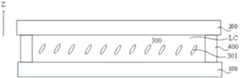
图1A为一种显示面板的截面图。如图1A所示,显示面板包括阵列基板100和对向基板200,阵列基板100和对向基板200相对设置,并通过封框胶400粘结形成液晶盒LC,液晶盒LC内设有液晶层300,液晶层300包括多个液晶分子301。像素电极和公共电极可位于阵列基板100中,以形成驱动液晶分子301旋转的平面电场。FIG. 1A is a cross-sectional view of a display panel. As shown in FIG. 1A, the display panel includes an
图1B为一种显示面板的平面图。图1B示出了显示面板包括多个子像素SP。多个子像素SP的设置方式不限于图1B所示,可根据需要而定。图1B示出了显示区R1和周边区R2,多个子像素SP位于显示区R1,图1B以周边区R2围绕显示区R1为例。周边区R2位于显示区R1的至少一侧。FIG. 1B is a plan view of a display panel. FIG. 1B shows that the display panel includes a plurality of sub-pixels SP. The arrangement of the multiple sub-pixels SP is not limited to that shown in FIG. 1B , and can be determined according to needs. FIG. 1B shows a display area R1 and a peripheral area R2, and a plurality of sub-pixels SP are located in the display area R1. FIG. 1B takes the peripheral area R2 surrounding the display area R1 as an example. The peripheral area R2 is located on at least one side of the display area R1.
在本公开的实施例的附图中,方向X、方向Y和方向Z为三个不同的方向,方向X和方向Y为平行于阵列基板100或对向基板200的主表面的方向,方向Z为垂直于方向X并垂直于方向Y的方向。例如,方向Z为阵列基板100或对向基板200的厚度方向。方向Z也可为阵列基板100指向对向基板200的方向。例如,方向X和方向Y相交。进一步例如,方向X和方向Y垂直。In the drawings of the embodiments of the present disclosure, the direction X, the direction Y and the direction Z are three different directions, the direction X and the direction Y are directions parallel to the main surface of the
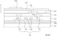
图2为本公开的实施例提供的一种显示面板中的阵列基板的布线结构图。图3为图2的沿线A1-A2的剖视图。图4为本公开的实施例提供的一种显示面板的示意图。如图2至图4所示,本公开的实施例提供的一种显示面板包括:阵列基板100和对向基板200,阵列基板100包括衬底基板101和位于衬底基板101上的多个子像素SP,每个子像素SP包括像素电极PE、公共电极CE、栅线GL、以及数据线DL,子像素SP为最小显示单元;对向基板200与阵列基板100相对设置,像素电极PE与公共电极CE不同层,公共电极CE和像素电极PE中靠近对向基板200的一个具有开口001,像素电极PE和公共电极CE被配置为形成电场,公共电极CE与像素电极PE在垂直于阵列基板100的方向上交叠以形成存储电容Cst。公共电极CE与像素电极PE在垂直于阵列基板100的方向上不交叠的部分形成电场FL。如图4所示,开口001与像素电极PE在垂直于阵列基板100的方向上交叠以形成电场FL。FIG. 2 is a wiring structure diagram of an array substrate in a display panel provided by an embodiment of the present disclosure. Fig. 3 is a cross-sectional view along line A1-A2 of Fig. 2 . FIG. 4 is a schematic diagram of a display panel provided by an embodiment of the present disclosure. As shown in FIG. 2 to FIG. 4 , a display panel provided by an embodiment of the present disclosure includes: an
例如,开口001的宽度为1μm-1.6μm,但不限于此,开口的宽度可根据需要而定。For example, the width of the
例如,数据线DL的宽度小于1.5μm。For example, the width of the data line DL is less than 1.5 μm.
例如,栅线GL和数据线DL彼此绝缘以被配置为分别输入信号。栅线GL被配置为输入扫描信号,数据线DL被配置为输入数据信号。公共电极PE被配置为输入固定电压。数据信号可通过打开的晶体管TR传输到像素电极PE上,像素电极PE和公共电极CE之间的电压差使得两者之间形成驱动液晶分子旋转的电场。For example, the gate line GL and the data line DL are insulated from each other to be configured to input signals, respectively. The gate lines GL are configured to input scan signals, and the data lines DL are configured to input data signals. The common electrode PE is configured to input a fixed voltage. The data signal can be transmitted to the pixel electrode PE through the turned-on transistor TR, and the voltage difference between the pixel electrode PE and the common electrode CE forms an electric field between the two to drive the liquid crystal molecules to rotate.
如图4所示,显示面板包括衬底基板101、缓冲层BF、绝缘层121、绝缘层122、绝缘层123、绝缘层124。As shown in FIG. 4 , the display panel includes a
例如,如图2至图4所示,显示面板还包括晶体管TR,晶体管TR包括有源层AL、以及与有源层AL相连的电极E1,像素电极PE通过过孔V1与电极E1相连。For example, as shown in FIGS. 2 to 4 , the display panel further includes a transistor TR. The transistor TR includes an active layer AL and an electrode E1 connected to the active layer AL. The pixel electrode PE is connected to the electrode E1 through a via hole V1 .
例如,如图2至图4所示,显示面板还包括数据线DL,晶体管TR还包括电极E2,数据线DL与电极E2相连。例如,电极E1可称作第一电极,电极E2可称作第二电极,但不限于此。For example, as shown in FIG. 2 to FIG. 4 , the display panel further includes a data line DL, the transistor TR further includes an electrode E2, and the data line DL is connected to the electrode E2. For example, the electrode E1 may be called a first electrode, and the electrode E2 may be called a second electrode, but not limited thereto.
例如,如图2至图4所示,电极E1和电极E2与有源层AL分别相连,电极E1通过过孔V2与有源层AL相连,并且电极E2通过过孔V3与有源层AL相连。For example, as shown in Figures 2 to 4, the electrode E1 and the electrode E2 are connected to the active layer AL respectively, the electrode E1 is connected to the active layer AL through the via hole V2, and the electrode E2 is connected to the active layer AL through the via hole V3 .
例如,如图3和图4所示,绝缘层121的厚度大于有源层AL的厚度。例如,有源层AL的厚度在30nm-60nm之间,绝缘层121的厚度为100-300nm。For example, as shown in FIGS. 3 and 4 , the thickness of the insulating
例如,如图2至图4所示,栅极GE的厚度范围为350-450nm,例如,栅线GL和栅线GE的材料包括金属,例如,金属包括钼、铝、钛、铜中的至少一种。For example, as shown in Figures 2 to 4, the thickness of the gate GE is in the range of 350-450nm, for example, the material of the grid line GL and the grid line GE includes metal, for example, the metal includes at least molybdenum, aluminum, titanium, copper A sort of.
例如,如图3和图4所示,绝缘层122的厚度范围为700-800nm。For example, as shown in FIGS. 3 and 4 , the thickness of the insulating
例如,如图2至图4所示,数据线DL、电极E2的厚度为200-350nm,材质包括金属,例如可为钼、铝、钛等金属层的至少两层结构构成,铝容易被氧化,需要设置夹层结构,确保铝层性能稳定,上层或下层金属选用氧化稳定性比铝强的金属层做界面层,例如,数据线DL、电极E2采用Ti/Al/Ti,但不限于此。For example, as shown in Figures 2 to 4, the thickness of the data line DL and the electrode E2 is 200-350nm, and the material includes metal, for example, it can be composed of at least two layers of metal layers such as molybdenum, aluminum, titanium, etc. Aluminum is easily oxidized , it is necessary to set up a sandwich structure to ensure that the performance of the aluminum layer is stable. The upper or lower metal layer uses a metal layer with stronger oxidation stability than aluminum as the interface layer. For example, the data line DL and the electrode E2 use Ti/Al/Ti, but not limited thereto.
例如,如图3和图4所示,绝缘层123的厚度范围为2000nm-3000nm。For example, as shown in FIG. 3 and FIG. 4 , the thickness of the insulating
图5A至图5G分别为图2中的单层的平面图。图6A和图6B为图2中的部分叠层的平面图。5A to 5G are plan views of the single layer in FIG. 2 , respectively. 6A and 6B are plan views of a portion of the stack in FIG. 2 .
图5A示出了有源层AL的平面图。图5A示出了有源层AL包括沟道AL0、导体区AL1、导体区AL2、以及导体区AL3。如图5A所示,导体区AL3位于两个沟道AL0之间,导体区AL1和导体区AL2之一为源极区,导体区AL1和导体区AL2之另一为漏极区。当然,本公开的实施例提供的一种显示面板中的有源层AL不限于图中所示,可根据需要而定。FIG. 5A shows a plan view of the active layer AL. FIG. 5A shows that the active layer AL includes a channel AL0 , a conductor area AL1 , a conductor area AL2 , and a conductor area AL3 . As shown in FIG. 5A , conductor region AL3 is located between two channels AL0 , one of conductor region AL1 and conductor region AL2 is a source region, and the other of conductor region AL1 and conductor region AL2 is a drain region. Of course, the active layer AL in the display panel provided by the embodiments of the present disclosure is not limited to what is shown in the figure, and can be determined according to requirements.
图5B示出了栅线GL的平面图,图5B示出了两条栅线GL。如图5B所示,栅极GE与栅线GL为一体结构。FIG. 5B shows a plan view of the gate lines GL, and FIG. 5B shows two gate lines GL. As shown in FIG. 5B , the gate GE and the gate line GL have an integral structure.
图5C示出了过孔V2和过孔V3的平面图。参考图3、图4、以及图5C,过孔V2贯穿绝缘层121和绝缘层122,过孔V3贯穿绝缘层121和绝缘层122。FIG. 5C shows a plan view of vias V2 and V3. Referring to FIG. 3 , FIG. 4 , and FIG. 5C , the via hole V2 penetrates the insulating
图5D示出了数据线DL、电极E1、电极E2。如图5D所示,电极E2和数据线DL为一体结构。FIG. 5D shows the data line DL, the electrode E1, and the electrode E2. As shown in FIG. 5D , the electrode E2 and the data line DL have an integrated structure.
图5E示出了过孔V1。参考图3、图4、以及图5E,像素电极PE通过过孔V1与电极E1相连。如图3和图4所示,过孔V1贯穿绝缘层123。FIG. 5E shows via V1. Referring to FIG. 3 , FIG. 4 , and FIG. 5E , the pixel electrode PE is connected to the electrode E1 through the via hole V1 . As shown in FIGS. 3 and 4 , the via hole V1 penetrates through the insulating
图5F示出了像素电极PE。多个像素电极PE可呈阵列排布。FIG. 5F shows the pixel electrode PE. A plurality of pixel electrodes PE may be arranged in an array.
图5G示出了公共电极CE。图5G以公共电极CE中的开口001示出该公共电极CE。Fig. 5G shows the common electrode CE. FIG. 5G shows the common electrode CE with an
参考图2至图4、图5B、以及图5D,显示面板还包括栅线GL和数据线DL,栅线GL和数据线DL交叉,晶体管TR还包括栅极GE和电极E2,数据线DL与电极E2相连,电极E2与有源层AL相连,栅线GL与栅极GE相连。Referring to FIG. 2 to FIG. 4, FIG. 5B, and FIG. 5D, the display panel further includes a gate line GL and a data line DL, the gate line GL and the data line DL intersect, the transistor TR also includes a gate GE and an electrode E2, and the data line DL and the data line DL intersect. The electrode E2 is connected, the electrode E2 is connected to the active layer AL, and the gate line GL is connected to the gate GE.
图6A示出了像素电极PE以及过孔V1的叠层图。FIG. 6A shows a stacked diagram of the pixel electrode PE and the via hole V1.
图6B示出了像素电极PE、过孔V1以及公共电极CE(以其中的开口001示出)的叠层图。FIG. 6B shows a stacked view of the pixel electrode PE, the via hole V1 and the common electrode CE (shown by the
例如,如图6B所示,开口001的宽度W8为1μm-1.6μm,相邻两列像素电极PE之间的间距W9为1.6μm。例如,开口001的宽度是指在垂直于开口001的延伸方向M上的尺寸。图中的虚线表示开口001的延伸方向M。例如,开口001的延伸方向M可以为开口的中线的延伸方向。例如,在本公开的实施例中,一个部件的延伸方向可指该部件的长度方向。For example, as shown in FIG. 6B , the width W8 of the
例如,参考图2和图6B,相邻两列像素电极PE之间在垂直于数据线DL的延伸方向上的间距W9与开口001的在垂直于数据线DL的延伸方向上的距离W7的比值为0.9-1.1。For example, referring to FIG. 2 and FIG. 6B, the ratio of the distance W9 between two adjacent columns of pixel electrodes PE in the direction perpendicular to the extension of the data line DL to the distance W7 of the
图7为本公开的实施例提供的一种显示面板中的阵列基板的布线结构图。图8为图7的沿线A3-A4的剖视图。图9为本公开的实施例提供的一种显示面板的示意图。FIG. 7 is a wiring structure diagram of an array substrate in a display panel provided by an embodiment of the present disclosure. Fig. 8 is a cross-sectional view along line A3-A4 of Fig. 7 . FIG. 9 is a schematic diagram of a display panel provided by an embodiment of the present disclosure.
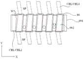
与图2所示的显示面板相比,图7所示的显示面板包括公共电极引线CEL。例如,公共电极引线CEL可采用金属制作。公共电极引线CEL可遮光。Compared with the display panel shown in FIG. 2, the display panel shown in FIG. 7 includes a common electrode lead CEL. For example, the common electrode lead CEL can be made of metal. The common electrode lead CEL can be light-shielded.
例如,如图7所示,显示面板还包括公共电极引线CEL,公共电极引线CEL与像素电极PE不同层,并且与公共电极CE不同层。For example, as shown in FIG. 7 , the display panel further includes a common electrode lead CEL, which has a different layer from the pixel electrode PE and a different layer from the common electrode CE.
例如,如图7所示,公共电极引线CEL与公共电极CE直接搭接。两个元件直接搭接是指该两个元件之间不设置绝缘层。For example, as shown in FIG. 7 , the common electrode lead CEL is directly overlapped with the common electrode CE. Two components directly overlapped means that no insulating layer is provided between the two components.
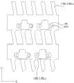
图10A为图7中的公共电极引线的平面图。图10B为图7中的数据线和公共电极引线的叠层图。图10C为图7中的数据线、栅线和公共电极引线的叠层图。FIG. 10A is a plan view of a common electrode lead in FIG. 7 . FIG. 10B is a stacked view of the data lines and common electrode leads in FIG. 7 . FIG. 10C is a stacked view of the data lines, gate lines and common electrode leads in FIG. 7 .
例如,如图6、图10A至图10C所示,公共电极引线CEL包括引线CEL1和引线CEL2,引线CEL1在衬底基板101上的正投影与数据线DL在衬底基板101上的正投影交叠,引线CEL2在衬底基板101上的正投影与栅线GL在衬底基板101上的正投影交叠,引线CEL1和引线CEL2在数据线DL和栅线GL交叉处相连。引线CEL1和引线CEL2横纵交错,可遮光,避免相邻子像素串扰,以提升显示品质。例如,在本公开的实施例中,引线CEL1可称作第一引线,引线CEL2可称作第二引线。For example, as shown in FIG. 6 and FIG. 10A to FIG. 10C, the common electrode lead CEL includes a lead CEL1 and a lead CEL2, and the orthographic projection of the lead CEL1 on the
例如,如图6、图10A至图10C所示,引线CEL1和引线CEL2为一体结构。For example, as shown in FIG. 6 , and FIG. 10A to FIG. 10C , the lead CEL1 and the lead CEL2 are integrally structured.
图11为本公开的实施例提供的一种显示面板中的阵列基板的布线结构图。例如,如图11所示,公共电极引线CEL包括引线CEL1和引线CEL2,引线CEL1在衬底基板101上的正投影与数据线DL在衬底基板101上的正投影交叠,引线CEL2在衬底基板101上的正投影与栅线GL在衬底基板101上的正投影交叠,引线CEL1的宽度小于引线CEL2的宽度。例如,如图11所示,引线CEL1和引线CEL2在数据线DL和栅线GL交叉处相连,但不限于此。FIG. 11 is a wiring structure diagram of an array substrate in a display panel provided by an embodiment of the present disclosure. For example, as shown in FIG. 11 , the common electrode lead CEL includes a lead CEL1 and a lead CEL2, the orthographic projection of the lead CEL1 on the
例如,如图11所示,引线CEL1和引线CEL2为一体结构。引线CEL1和引线CEL2由同一薄膜采用同一构图工艺形成。For example, as shown in FIG. 11 , the lead CEL1 and the lead CEL2 are integrally structured. The leads CEL1 and CEL2 are formed from the same film using the same patterning process.
例如,如图11所示,引线CEL2和栅线GL的交叠宽度W3与引线CEL1和数据线DL的交叠宽度W4的比值为1.5-2.5。For example, as shown in FIG. 11 , the ratio of the overlapping width W3 of the lead CEL2 and the gate line GL to the overlapping width W4 of the lead CEL1 and the data line DL is 1.5-2.5.
例如,如图11所示,晶体管TR包括有源层AL、以及与有源层AL相连的电极E1,像素电极PE通过过孔V1与电极E1相连,至少超过50%的子像素SP中的引线CEL2在衬底基板101上的正投影与过孔V1在衬底基板101上的正投影交叠。公共电极引线CEL不透光,且覆盖过孔V1,有效控制过孔V1对光线的弯曲散射而造成在观看侧的沿着栅线侧的漏光效应。For example, as shown in FIG. 11, the transistor TR includes an active layer AL, and an electrode E1 connected to the active layer AL. The pixel electrode PE is connected to the electrode E1 through a via hole V1. At least 50% of the leads in the sub-pixel SP The orthographic projection of CEL2 on the
例如,如图11所示,引线CEL2的宽度小于6.2μm,并且大于2.5μm。进一步例如,引线CEL2的宽度大于5μm。For example, as shown in FIG. 11 , the width of the lead CEL2 is smaller than 6.2 μm and larger than 2.5 μm. As a further example, the width of the lead CEL2 is greater than 5 μm.
过孔V1的下底面的目前的最小工艺直径为2.5μm,将引线CEL2的宽度设置的较宽,可以使得公共电极引线至少覆盖相邻两行子像素之间的过孔V1的侧面的部分,起到遮光作用,提升显示效果。The current minimum process diameter of the lower bottom of the via hole V1 is 2.5 μm, and setting the width of the lead CEL2 wider can make the common electrode lead cover at least part of the side of the via hole V1 between two adjacent rows of sub-pixels, Play a shading effect and improve the display effect.
例如,如图11所示,引线CEL1的宽度小于3.2μm。For example, as shown in FIG. 11 , the width of the lead CEL1 is smaller than 3.2 μm.
例如,如图7和图11所示,公共电极引线CEL在衬底基板101上的正投影与像素电极PE在衬底基板101上的正投影交叠。For example, as shown in FIG. 7 and FIG. 11 , the orthographic projection of the common electrode lead CEL on the
例如,如图11所示,像素电极PE在衬底基板101上的正投影与引线CEL2在衬底基板101上的正投影的交叠。For example, as shown in FIG. 11 , the orthographic projection of the pixel electrode PE on the
例如,如图11所示,像素电极PE在衬底基板101上的正投影与引线CEL1在衬底基板101上的正投影的交叠,引线CEL1遮光,提升子像素边缘处的显示效果,利于提升显示品质。For example, as shown in FIG. 11 , when the orthographic projection of the pixel electrode PE on the
例如,如图11所示,为了获得较好的显示效果,引线CEL1和数据线DL的交叠宽度为W1,像素电极PE在衬底基板101上的正投影与引线CEL1在衬底基板101上的正投影的交叠宽度为W2,W2/W1>25%。For example, as shown in FIG. 11, in order to obtain a better display effect, the overlapping width of the lead CEL1 and the data line DL is W1, and the orthographic projection of the pixel electrode PE on the
例如,交叠宽度W2的范围为1μm-1.5μm。For example, the overlapping width W2 ranges from 1 μm to 1.5 μm.
图12为本公开的实施例提供的一种显示面板中的子像素的布图面积的示意图。图13为本公开的实施例提供的一种显示面板中的子像素的布图面积的示意图。图14为本公开的实施例提供的一种显示面板中的子像素中的公共电极和像素电极的交叠面积的示意图。图15为本公开的实施例提供的一种显示面板中的子像素中的公共电极或像素电极中的开口的面积的示意图。图16为本公开的实施例提供的一种显示面板中的子像素的透光面积的示意图。图17为本公开的实施例提供的一种显示面板中的子像素的透光面积的示意图。FIG. 12 is a schematic diagram of a layout area of sub-pixels in a display panel provided by an embodiment of the present disclosure. FIG. 13 is a schematic diagram of a layout area of sub-pixels in a display panel provided by an embodiment of the present disclosure. FIG. 14 is a schematic diagram of an overlapping area of a common electrode and a pixel electrode in a sub-pixel in a display panel provided by an embodiment of the present disclosure. FIG. 15 is a schematic diagram of an area of a common electrode in a sub-pixel or an opening in a pixel electrode in a display panel provided by an embodiment of the present disclosure. FIG. 16 is a schematic diagram of a light transmission area of a sub-pixel in a display panel provided by an embodiment of the present disclosure. FIG. 17 is a schematic diagram of a light-transmitting area of a sub-pixel in a display panel provided by an embodiment of the present disclosure.
例如,在显示面板的可视区域内,子像素SP的布图面积为S,像素电极PE的布图面积为S1,在子像素SP中,公共电极CE在衬底基板101上的正投影与像素电极PE在衬底基板101上的正投影的交叠面积为S2;,在子像素SP中,开口001的面积为S3,子像素SP的透光面积为S4,则显示面板中的至少一个子像素满足:S1/S≥0.62,S2/S≥0.31,0.31≥S3/S≥0.21,0.36≤S4/S≤0.53。例如,S2/S≥0.42。例如,S4/S≥0.51。For example, in the visible area of the display panel, the layout area of the sub-pixel SP is S, and the layout area of the pixel electrode PE is S1. In the sub-pixel SP, the orthographic projection of the common electrode CE on the
本公开的实施例提供的一种显示面板,满足上述比例关系中至少之一,各面积比例值的协调性好,利于提高显示效果,利于得到高像素密度(Pixels Per Inch,PPI)、高扫描频率的平面电场显示面板。A display panel provided by an embodiment of the present disclosure satisfies at least one of the above proportional relationships, and the coordination of each area ratio is good, which is conducive to improving the display effect and obtaining high pixel density (Pixels Per Inch, PPI), high scanning frequency of the flat electric field display panel.
例如,为了进一步提升显示品质,显示面板中的至少一个子像素满足:S1/S≥0.81,S2/S≥0.59,S3/S≥0.22,S4/S≥0.46。For example, in order to further improve the display quality, at least one sub-pixel in the display panel satisfies: S1/S≥0.81, S2/S≥0.59, S3/S≥0.22, S4/S≥0.46.
图12和图13示出了每个子像素SP的布图面积S。图14示出了公共电极CE在衬底基板101上的正投影与像素电极PE在衬底基板101上的正投影的交叠面积S2。图15示出了开口001的面积S3。图16和图17示出了子像素SP的透光面积S4。子像素SP的透光面积S4是指子像素SP的透光区域的面积。12 and 13 show the layout area S of each sub-pixel SP. FIG. 14 shows the overlapping area S2 of the orthographic projection of the common electrode CE on the
例如,在一些实施例中,在一个子像素SP中,相邻的引线CEL1和相邻的引线CEL2围设的区域为透光区域,该透光区域的面积即为透光面积S4。例如,透光面积S4是阵列基板和对向基板共同约束出来的面积。For example, in some embodiments, in a sub-pixel SP, the area surrounded by the adjacent lead CEL1 and the adjacent lead CEL2 is the light-transmitting area, and the area of the light-transmitting area is the light-transmitting area S4 . For example, the light transmission area S4 is the area constrained by the array substrate and the opposite substrate.
例如,显示面板的可视区域是指显示面板的显示区R1(如图1B所示),或者是指阵列基板100的显示区,或者是指对向基板200的显示区。For example, the visible area of the display panel refers to the display area R1 of the display panel (as shown in FIG. 1B ), or refers to the display area of the
例如,如图12和图13所示,布图面积S可为多条栅线GL和多条数据线DL交叉形成的多个区域内的一个区域的面积。一个子像素SP包括一个晶体管、一个像素电极、公共电极中的至少一个开口001。一个子像素SP还可包括一条栅线GL和一条数据线DL。For example, as shown in FIG. 12 and FIG. 13 , the layout area S may be an area of a region among the regions formed by intersections of a plurality of gate lines GL and a plurality of data lines DL. A sub-pixel SP includes a transistor, a pixel electrode, and at least one
例如,如图14所示,交叠面积S2可指像素电极PE和公共电极CE在方向Z上交叠的部分的面积。For example, as shown in FIG. 14 , the overlapping area S2 may refer to an area of a portion where the pixel electrode PE and the common electrode CE overlap in the direction Z. Referring to FIG.
例如,在一些实施例中,显示面板中的至少一个子像素满足:S1/S≥0.81,S2/S≥0.59,S3/S≥0.22,S4/S≥0.46。For example, in some embodiments, at least one sub-pixel in the display panel satisfies: S1/S≥0.81, S2/S≥0.59, S3/S≥0.22, S4/S≥0.46.
图15以开口001设置在公共电极CE中为例进行说明。在其他的实施例中,开口001也可以设置在像素电极PE中。只要是将开口001设置在公共电极CE和像素电极PE中靠近对向基板200中的一个之中即可。或者也可以说,开口001设置在公共电极CE和像素电极PE中远离衬底基板101中的一个之中。FIG. 15 is illustrated by taking the
对于子像素SP的透光面积S4,如图16和图17所示,在每个子像素SP的布图面积S内,可透过光的区域的面积。对于显示面板,该透光面积S4可由阵列基板100和对向基板200共同限定,或者由阵列基板100和对向基板200之一限定。在透光面积S4由阵列基板100和对向基板200共同限定的情况下,对于一个子像素SP,阵列基板的透光部分和对向基板的透光部分的交集即为子像素SP的透光面积S4。即,透光面积S4是阵列基板的透光部分和对向基板的透光部分的交集的面积。For the light transmission area S4 of the sub-pixel SP, as shown in FIG. 16 and FIG. 17 , the area of the light-transmitting area within the layout area S of each sub-pixel SP. For a display panel, the light-transmitting area S4 can be defined jointly by the
例如,在子像素SP中,像素电极PE和公共电极CE采用透明导电材料制作,可透过光,而栅线GL、数据线DL、公共电极引线CEL均采用金属材料制作,可遮挡光。从而,例如,透明导电材料包括氧化铟锡,但不限于此。For example, in the sub-pixel SP, the pixel electrode PE and the common electrode CE are made of transparent conductive material, which can transmit light, while the gate line GL, data line DL, and common electrode lead CEL are all made of metal material, which can block light. Thus, for example, the transparent conductive material includes indium tin oxide, but is not limited thereto.
图18为本公开一实施例提供的一种显示面板中的像素电极和公共电极中的开口的叠层图。FIG. 18 is a stacked diagram of openings in a pixel electrode and a common electrode in a display panel provided by an embodiment of the present disclosure.
如图18所示,像素电极PE设置在公共电极CE的下方,公共电极CE具有开口001,像素电极PE具有中线CL0,开口001具有中线C0,如图18所示,公共电极CE的开口001的中线C0与像素电极PE的中线CL0具有走向相同的部分。As shown in Figure 18, the pixel electrode PE is arranged below the common electrode CE, the common electrode CE has an
如图18所示,开口001的中线C0与像素电极PE的中线CL0的走向相同的部分的长度与像素电极PE的中线CL0的长度的比值大于50%,开口001的中线C0与像素电极PE的中线CL0的走向相同的部分的长度与开口001的中线C0的长度的比值大于65%。As shown in FIG. 18 , the ratio of the length of the part where the center line C0 of the
例如,开口001的中线C0与像素电极PE的中线CL0的走向相同的部分的长度与像素电极PE的中线CL0的长度的比值小于90%,开口001的中线C0与像素电极PE的中线CL0的走向相同的部分的长度与开口001的中线C0的长度的比值小于95%。For example, the ratio of the length of the part where the centerline C0 of the
如图18所示,公共电极CE的开口001的中线C0与像素电极PE的中线CL0至少部分重合。As shown in FIG. 18 , the centerline C0 of the
如图18所示,中线CL0和中线C0的重合长度大于像素电极的中线CL0的长度的50%。中线CL0和中线C0的重合长度大于公共电极CE的开口001的中线C0的长度的65%。重合包括完全重合以及小于1微米的偏差。As shown in FIG. 18 , the overlapping length of the center line CL0 and the center line C0 is greater than 50% of the length of the center line CL0 of the pixel electrode. The coincident length of the centerline CLO and the centerline C0 is greater than 65% of the length of the centerline C0 of the
如图18所示,开口001的中线C0与像素电极PE的中线CL0的重合长度与像素电极PE的中线CL0的长度的比值大于50%,开口001的中线C0与像素电极PE的中线CL0的重合长度与开口001的中线C0的长度的比值大于65%。As shown in FIG. 18 , the ratio of the overlapping length of the central line C0 of the
例如,如图18所示,开口001的中线C0与像素电极PE的中线CL0的重合长度与像素电极PE的中线CL0的长度的比值小于90%,开口001的中线C0与像素电极PE的中线CL0的重合长度与开口001的中线C0的长度的比值小于95%。For example, as shown in FIG. 18, the ratio of the overlapping length of the central line C0 of the
如图18所示,开口001的靠近过孔V1的一端不超出像素电极PE,而开口001的远离过孔V1的一端超出像素电极PE。As shown in FIG. 18 , the end of the
如图18所示,开口001的边界与像素电极PE的边界在垂直于中线C0的方向上的距离d在各处不完全相等。例如,距离d的范围在0.3-9μm。该距离d不相等可以在子像素的显示区形成与像素电极边界或者公共电极的开口的边界不平行的光学渐变区域,起到多畴的显示效果。因为像素电极和公共电极为透明电极,在靠近该子像素的电极E1的边界和相邻子像素的电极E1的边界区域,像素电极和公共电极的交叠边界不平行,可以起到增加显示畴的效果。As shown in FIG. 18 , the distance d between the boundary of the
如图18所示,从靠近过孔V1的位置指向远离过孔V1的位置的方向上,在中心C0的至少一侧(图18中的左侧),开口001的边界与像素电极PE的边界在垂直于中心C0的方向上的距离d逐渐减小。As shown in FIG. 18, in the direction from the position close to the via hole V1 to the position away from the via hole V1, on at least one side of the center C0 (the left side in FIG. 18), the boundary of the
图19为本公开另一实施例提供的一种显示面板中的阵列基板的示意图。如图19所示,像素电极PE的靠近数据线DL的边缘为曲线,以形成多畴显示的效果。FIG. 19 is a schematic diagram of an array substrate in a display panel provided by another embodiment of the present disclosure. As shown in FIG. 19 , the edge of the pixel electrode PE close to the data line DL is curved to form a multi-domain display effect.
如图19所示,开口001的边界与像素电极PE的边界在垂直于数据线DL的延伸方向的方向上的距离d1在各处不完全相等。如图19所示,数据线DL沿方向Y延伸,距离d1可为开口001的边界与像素电极PE的边界在方向X上的最小距离。例如,距离d1的范围在0.3-3μm。As shown in FIG. 19 , the distance d1 between the boundary of the
图20为本公开另一实施例提供的一种显示面板中的阵列基板的示意图。如图20所示,在同一子像素SP中,像素电极PE的外边缘G1设置在公共电极CE的外边缘G2以内,并且与过孔V1的距离越远,单位长度上的交叠面积S2越小。例如,如图20所示,沿数据线DL的延伸方向,与过孔V1的距离越远,单位长度上的交叠面积S2越小。FIG. 20 is a schematic diagram of an array substrate in a display panel provided by another embodiment of the present disclosure. As shown in FIG. 20, in the same sub-pixel SP, the outer edge G1 of the pixel electrode PE is set within the outer edge G2 of the common electrode CE, and the farther the distance from the via hole V1 is, the smaller the overlapping area S2 per unit length is. Small. For example, as shown in FIG. 20 , along the extending direction of the data line DL, the farther the distance from the via hole V1 is, the smaller the overlapping area S2 per unit length is.
例如,如图20所示,像素电极PE包括依次设置的连接部CP、主体部P1、以及主体部P2,连接部CP与电极E1(如图3所示)相连,主体部P1和主体部P2分别设置在像素电极PE的中线CL1的两侧,中线CL1的延伸方向垂直于数据线DL的延伸方向。如图20所示,中线CL1为像素电极PE的除了连接部CP之外的部分的中线。如图20所示,中线CL1的延伸方向与栅线GL的延伸方向相同。For example, as shown in FIG. 20, the pixel electrode PE includes a connecting portion CP, a main body P1, and a main body P2 arranged in sequence. The connecting portion CP is connected to the electrode E1 (as shown in FIG. 3 ), and the main body P1 and the main body P2 They are respectively arranged on both sides of the center line CL1 of the pixel electrode PE, and the extension direction of the center line CL1 is perpendicular to the extension direction of the data line DL. As shown in FIG. 20 , the center line CL1 is the center line of the portion of the pixel electrode PE other than the connection portion CP. As shown in FIG. 20, the extension direction of the center line CL1 is the same as the extension direction of the gate line GL.
例如,如图20所示,为了兼顾水平电场和存储电容,主体部P1与公共电极CE形成的电容的交叠面积为SP1,主体部P2与公共电极CE形成的电容的交叠面积为SP2,SP1大于SP2。例如,SP1大于2*SP2。在本公开的实施例中,“*”表示乘号。For example, as shown in FIG. 20, in order to take into account both the horizontal electric field and the storage capacitance, the overlapping area of the capacitance formed by the main body P1 and the common electrode CE is SP1, and the overlapping area of the capacitance formed by the main body P2 and the common electrode CE is SP2, SP1 is greater than SP2. For example, SP1 is greater than 2*SP2. In an embodiment of the present disclosure, "*" represents a multiplication sign.
图20还示出了像素电极PE的沿数据线DL的延伸方向延伸的中线CL0。例如,像素电极PE可相对于中线CL0呈轴对称。FIG. 20 also shows the center line CL0 of the pixel electrode PE extending along the extending direction of the data line DL. For example, the pixel electrode PE may be axisymmetric with respect to the centerline CL0.
图21为本公开另一实施例提供的一种显示面板中的阵列基板的示意图。例如,如图21所示,子像素SP在数据线DL的延伸方向上包括多个子区域R01,每个子区域R01设置有至少两个光学子区域PR01,光学子区域PR01相对于像素电极PE的中线CL0对称分布,中线CL0的延伸方向与数据线DL的延伸方向相同。FIG. 21 is a schematic diagram of an array substrate in a display panel provided by another embodiment of the present disclosure. For example, as shown in FIG. 21, the sub-pixel SP includes a plurality of sub-regions R01 in the extending direction of the data line DL, each sub-region R01 is provided with at least two optical sub-regions PR01, and the optical sub-region PR01 is opposite to the centerline of the pixel electrode PE The distribution of CL0 is symmetrical, and the extension direction of the center line CL0 is the same as the extension direction of the data line DL.
例如,如图21所示,像素电极PE沿数据线DL的延伸方向被分为多个子区域R01,在至少一个子区域R01内,单位长度上的交叠面积S2沿数据线DL的延伸方向非线性变化。非线性变化的交叠面积S2,可以减少线性变化造成的光学衍射条纹与像素显示画面的相互干扰。For example, as shown in FIG. 21 , the pixel electrode PE is divided into a plurality of sub-regions R01 along the extending direction of the data line DL, and in at least one sub-region R01, the overlapping area S2 per unit length is different along the extending direction of the data line DL. linear change. The non-linearly changing overlapping area S2 can reduce the mutual interference between the optical diffraction fringes and the pixel display picture caused by the linear changing.
例如,如图21所示,在至少一个子区域内,从靠近像素电极PE与电极E1的连接位置(过孔V1处)到远离像素电极PE与电极E1的连接位置的方向上,即,从上至下的方向上,交叠面积S2沿数据线DL的延伸方向非线性减小。For example, as shown in FIG. 21, in at least one sub-region, from the direction close to the connection position between the pixel electrode PE and the electrode E1 (at the via hole V1) to away from the connection position between the pixel electrode PE and the electrode E1, that is, from In the direction from top to bottom, the overlapping area S2 decreases non-linearly along the extending direction of the data line DL.
例如,如图21所示,显示面板至少包含一个光学子区域PR01的长轴方向与存储电容Cst的像素电极PE的边缘的走向之间的夹角A0小于15°。For example, as shown in FIG. 21 , the display panel includes at least one optical sub-region PR01 and the angle A0 between the long axis direction of the pixel electrode PE of the storage capacitor Cst is less than 15°.
图22为本公开一实施例提供的一种显示面板的示意图。图23为本公开一实施例提供的一种显示面板的示意图。FIG. 22 is a schematic diagram of a display panel provided by an embodiment of the present disclosure. FIG. 23 is a schematic diagram of a display panel provided by an embodiment of the present disclosure.
例如,如图22和图23所示,显示面板还包括隔垫物PS,对向基板200包括衬底基板201,隔垫物PS设置在衬底基板201上,公共电极引线CEL具有镂空部002,阵列基板100在镂空部002处形成凹陷RS,隔垫物PS在衬底基板101上的正投影与凹陷RS在衬底基板101上的正投影交叠。如图22和图23所示,镂空部002为开口。例如,镂空部002的宽度为1.0μm-1.6μm,但不限于此。For example, as shown in FIG. 22 and FIG. 23 , the display panel further includes a spacer PS, the
例如,如图23所示,凹陷RS被配置为对隔垫物PS进行限位。For example, as shown in FIG. 23 , the recess RS is configured to limit the spacer PS.
图24为本公开一实施例提供的一种显示面板的示意图。例如,如图24所示,隔垫物PS与阵列基板100之间具有间隙G0,隔垫物PS被配置为被挤压时与阵列基板100接触。FIG. 24 is a schematic diagram of a display panel provided by an embodiment of the present disclosure. For example, as shown in FIG. 24 , there is a gap G0 between the spacer PS and the
例如,如图23和图24所示,隔垫物PS包括主隔垫物PS1和辅隔垫物PS2,主隔垫物PS1与阵列基板100接触,辅隔垫物PS2与阵列基板100之间具有间隙G0。For example, as shown in FIG. 23 and FIG. 24, the spacer PS includes a main spacer PS1 and an auxiliary spacer PS2, the main spacer PS1 is in contact with the
例如,如图24所示,间隙G0的高度为50-200nm。For example, as shown in FIG. 24, the height of the gap G0 is 50-200 nm.
例如,如图23和图24所示,主隔垫物PS1和辅隔垫物PS2的高度差为51nm到200nm之间。为了使得隔垫物PS与阵列基板100之间具有间隙G0,可以使得主隔垫物PS1和辅隔垫物PS2的高度不一样,即,主隔垫物PS1的高度大于辅隔垫物PS2的高度。For example, as shown in FIG. 23 and FIG. 24 , the height difference between the main spacer PS1 and the auxiliary spacer PS2 is between 51 nm and 200 nm. In order to have a gap G0 between the spacer PS and the
图25为本公开一实施例提供的一种显示面板的示意图。例如,如图25所示,为了更好的支撑主隔垫物PS1和对主隔垫物PS1进行限位,并提升显示品质,显示面板还包括遮光衬垫80,镂空部002在阵列基板100上的正投影落入遮光衬垫80在阵列基板100上的正投影内。遮光衬垫80起到遮光作用,以避免光线影响晶体管TR的有源层AL。当然,在一些实施例中,也可以不设置遮光衬垫80。FIG. 25 is a schematic diagram of a display panel provided by an embodiment of the present disclosure. For example, as shown in FIG. 25 , in order to better support and limit the main spacer PS1 and improve the display quality, the display panel further includes a light-
例如,如图24和图25所示,在主隔垫物PS1处,凹陷RS被遮光衬垫80填充,在辅隔垫物PS2处,不设置遮光衬垫80,以使得辅隔垫物PS2与阵列基板100之间具有间隙G0。例如,遮光衬垫80在衬底基板101上的正投影与辅隔垫物PS2在衬底基板101上的正投影不交叠,遮光衬垫80在衬底基板101上的正投影与主隔垫物PS1在衬底基板101上的正投影交叠。For example, as shown in FIGS. 24 and 25, at the main spacer PS1, the recess RS is filled with a light-
图23至图25还示出了缓冲层BF1,缓冲层BF1位于衬底基板101上,遮光层601位于缓冲层BF1上,缓冲层BF设置遮光层601上。当然,在另一些实施例中,也可以不设置遮光层601。23 to 25 also show the buffer layer BF1, the buffer layer BF1 is located on the
例如,如图23至图25所示,显示面板还包括遮光层601,遮光层601位于有源层AL和衬底基板101之间,有源层AL在衬底基板101上的正投影落入遮光层601在衬底基板101上的正投影内。For example, as shown in FIGS. 23 to 25 , the display panel further includes a light-
例如,为了便于制作,主隔垫物PS1的高度等于辅隔垫物PS2的高度。隔垫物PS的高度是指在隔垫物PS在方向Z上的尺寸。For example, for ease of manufacture, the height of the main spacer PS1 is equal to the height of the auxiliary spacer PS2. The height of the spacer PS refers to the dimension of the spacer PS in the direction Z.
例如,如图24和图25所示,显示面板还包括隔垫物PS和遮光衬垫80,隔垫物PS包括主隔垫物PS1和辅隔垫物PS2,主隔垫物PS1与阵列基板100接触,辅隔垫物PS2与阵列基板100之间具有间隙G0,公共电极引线CEL具有多个镂空部002,遮光衬垫80设置在多个镂空部中的部分镂空部处,阵列基板100在多个镂空部002中的另一部分镂空部处形成凹陷RS,辅隔垫物PS2在衬底基板101上的正投影与凹陷RS在衬底基板101上的正投影交叠,主隔垫物PS1在衬底基板101上的正投影与凹陷RS在衬底基板101上的正投影不交叠。即,在主隔垫物PS1处,设置遮光衬垫80,而在辅隔垫物PS2处,不设置遮光衬垫80。在液晶盒对位的时候,凹陷RS与对应位置处的辅隔垫物PS2不接触,在发生具有垂直于阵列基板(方向Z)的分压的挤压时,辅隔垫物PS2与凹陷RS接触。如图24所示,辅隔垫物PS2处的镂空部002不设置遮光衬垫80以设有凹陷RS。如图25所示,主隔垫物PS1处的镂空部002被遮光衬垫80填充。For example, as shown in FIGS. 24 and 25, the display panel further includes a spacer PS and a light-
图26为本公开的实施例提供的一种显示面板中的隔垫物的平面图。例如,如图26所示,隔垫物PS为多个,多个隔垫物PS可呈正多边形排列。FIG. 26 is a plan view of a spacer in a display panel provided by an embodiment of the present disclosure. For example, as shown in FIG. 26 , there are a plurality of spacers PS, and the plurality of spacers PS can be arranged in a regular polygon.
例如,如图26所示,多个隔垫物PS呈正方形排列,正方形的两条对角线之一的延伸方向平行于栅线GL的延伸方向,正方形的两条对角线之另一的延伸方向平行于数据线DL的延伸方向。图26示出了对角线901沿方向X延伸,对角线902沿方向Y延伸。参考图2和图26,对角线901的延伸方向平行于栅线GL的延伸方向,对角线902的延伸方向平行于数据线DL的延伸方向。例如,对角线901垂直于对角线902。For example, as shown in Figure 26, a plurality of spacers PS are arranged in a square, the extension direction of one of the two diagonals of the square is parallel to the extension direction of the grid line GL, and the extension direction of the other two diagonals of the square is The extending direction is parallel to the extending direction of the data line DL. FIG. 26 shows that the
例如,如图26所示,主隔垫物PS1的个数小于辅隔垫物PS2的个数。例如,主隔垫物PS1和辅隔垫物PS2的个数比例为0.1-0.3。For example, as shown in FIG. 26, the number of main spacers PS1 is smaller than the number of auxiliary spacers PS2. For example, the number ratio of the main spacer PS1 to the auxiliary spacer PS2 is 0.1-0.3.
图27A为本公开的实施例提供的一种显示面板中的遮光层、公共电极引线和遮光衬垫的示意图。图27B为本公开的另一实施例提供的一种显示面板中的遮光层、公共电极引线和遮光衬垫的示意图。FIG. 27A is a schematic diagram of a light-shielding layer, common electrode leads and light-shielding pads in a display panel provided by an embodiment of the present disclosure. FIG. 27B is a schematic diagram of a light-shielding layer, common electrode leads and light-shielding pads in a display panel provided by another embodiment of the present disclosure.
例如,如图27A所示,遮光衬垫80至少部分覆盖镂空部002,即,遮光衬垫80在衬底基板101上的正投影与镂空部002在衬底基板101上的正投影交叠。For example, as shown in FIG. 27A , the light-
例如,如图27A所示,遮光衬垫80在衬底基板101上的正投影与遮光层601在衬底基板101上的正投影交叠,在遮光衬垫80或引线CEL1的一侧,遮光衬垫80超出遮光层601的尺寸W5为0.2-1.5μm,即,遮光衬垫80向子像素的中心区域偏移的距离为0.2-1.5μm。参考图23,遮光层601位于有源层AL和衬底基板101之间。For example, as shown in FIG. 27A, the orthographic projection of the light-
例如,如图27A所示,遮光衬垫80的平行于栅线GL的延伸方向的边缘比遮光层601的平行于栅线GL的延伸方向的边缘更靠近相应子像素SP的中心区域。For example, as shown in FIG. 27A , the edge of the light-shielding
如图27B所示,相邻两个镂空部002共用同一个遮光衬垫80。As shown in FIG. 27B , two adjacent
例如,如图8、图9、图23至图25所示,晶体管TR包括有源层AL、以及与有源层AL相连的电极E1,像素电极PE通过过孔V1与电极E1相连,公共电极引线CEL在衬底基板101上的正投影至少覆盖过孔V1的部分斜面在衬底基板101上的正投影。例如,如图23所示,斜面Vs的被公共电极引线CEL覆盖的部分的上边缘的倾角Aa为23度-29度。For example, as shown in FIG. 8, FIG. 9, and FIG. 23 to FIG. 25, the transistor TR includes an active layer AL and an electrode E1 connected to the active layer AL, the pixel electrode PE is connected to the electrode E1 through a via hole V1, and the common electrode The orthographic projection of the lead CEL on the
图28为本公开的实施例提供的一种阵列基板的剖视图。图29为本公开的另一实施例提供的一种阵列基板的剖视图。FIG. 28 is a cross-sectional view of an array substrate provided by an embodiment of the present disclosure. FIG. 29 is a cross-sectional view of an array substrate provided by another embodiment of the present disclosure.
如图28所示,与图3所示的阵列基板相比,像素电极PE和电极E1之间没有设置绝缘层123,像素电极PE和电极E1直接搭接。即,没有设置过孔V1。As shown in FIG. 28 , compared with the array substrate shown in FIG. 3 , no insulating
图29中的截面图未示出开口001,公共电极CE中的开口001设置在图29未示出的其他位置处。The cross-sectional view in FIG. 29 does not show the
图30为本公开的另一实施例提供的一种阵列基板的剖视图。图30中的电极E1也采用透明导电材料,例如氧化铟锡来制作。在图30所示的阵列基板中,公共电极CE位于公共电极引线CEL之上。公共电极引线CEL在衬底基板101上的正投影与像素电极PE在衬底基板101上的正投影交叠。FIG. 30 is a cross-sectional view of an array substrate provided by another embodiment of the present disclosure. The electrode E1 in FIG. 30 is also made of a transparent conductive material, such as indium tin oxide. In the array substrate shown in FIG. 30, the common electrode CE is located above the common electrode lead CEL. The orthographic projection of the common electrode lead CEL on the
如图30所示,衬底基板101上设有导电图案层LYa,导电图案层LYa上设有绝缘层GI,绝缘层GI上设有半导体层LYb,半导体层LYb上设有绝缘层ILD1,绝缘层ILD1上设有半导体层LY0,半导体层LY0上设有绝缘层ILD2,绝缘层ILD2上设有导电图案层LY1,导电图案层LY1上设有绝缘层ILD3,绝缘层ILD3上设有导电图案层LY2,导电图案层LY2上设有绝缘层PVX1,绝缘层PVX1上设有导电图案层LY3,导电图案层LY3上设有绝缘层PLN,绝缘层PLN上设有像素电极PE,像素电极PE上设有绝缘层PVX2,绝缘层PVX2上设有公共电极引线CEL,公共电极引线CEL上设有公共电极CE,隔垫物PS设在公共电极CE上。As shown in FIG. 30 , the
例如,如图30所示,导电图案层LYa、导电图案层LY1导电图案层LY2、以及公共电极引线CEL均采用金属制作。导电图案层LY3、像素电极PE、公共电极CE可采用透明导电材料,例如,透明导电材料包括透明导电氧化物材料例如氧化铟锡。For example, as shown in FIG. 30, the conductive pattern layer LYa, the conductive pattern layer LY1, the conductive pattern layer LY2, and the common electrode lead CEL are all made of metal. The conductive pattern layer LY3 , the pixel electrode PE, and the common electrode CE can use transparent conductive materials, for example, the transparent conductive materials include transparent conductive oxide materials such as indium tin oxide.
如图30所示,隔垫物PS位于阵列基板中。在本公开的实施例中,隔垫物可以设置在衬底基板101上,即,位于阵列基板100中,也可以设置在衬底基板201上,即,位于对向基板200中。As shown in FIG. 30 , the spacers PS are located in the array substrate. In an embodiment of the present disclosure, the spacer may be disposed on the
如图30所示,导电图案层LYa包括栅极GE02、栅极GE1、以及导电部92a,半导体层LYb包括有源层ALT,导电图案层LY1包括电极Ea、电极Eb、栅极GE01、以及导电部921,导电图案层LY2包括导电部922和电极E2,导电图案层LY3包括电极E1。电极Ea和电极Eb之一为晶体管的源极,电极Ea和电极Eb之另一为晶体管的漏极。栅极GE02和栅极GE01构成晶体管TR的栅极GE。栅极GE02也可看做遮光层。例如,在一些实施例中,栅极GE02和栅极GE01彼此相连,但不限于此,在另一些实施例中,栅极GE02和栅极GE01可以彼此绝缘。As shown in FIG. 30, the conductive pattern layer LYa includes a gate GE02, a gate GE1, and a
例如,如图30所示,绝缘层GI可称作栅极绝缘层,绝缘层ILD1可称作层间绝缘层,绝缘层ILD2可称作层间绝缘层,绝缘层ILD3可称作层间绝缘层,绝缘层PVX1可称作钝化层,绝缘层PVX2可称作钝化层,绝缘层PLN可称作平坦层。For example, as shown in FIG. 30, the insulating layer GI may be called a gate insulating layer, the insulating layer ILD1 may be called an interlayer insulating layer, the insulating layer ILD2 may be called an interlayer insulating layer, and the insulating layer ILD3 may be called an interlayer insulating layer. layer, the insulating layer PVX1 may be called a passivation layer, the insulating layer PVX2 may be called a passivation layer, and the insulating layer PLN may be called a planarization layer.
例如,如图30所示,显示面板包括晶体管TR和晶体管TR1,晶体管TR位于显示区,晶体管TR1位于周边区,有源层AL和有源层ALT之一的材料为多晶硅,有源层AL和有源层ALT之另一的材料为氧化物半导体。在一个实施例中,有源层ALT的材料为多晶硅,有源层AL的材料为氧化物半导体。例如,多晶硅包括低温多晶硅(“Low Temperature Poly-Silicon,LTPS),氧化物半导体包括氧化铟镓锌(Indium Gallium Zinc Oxide,IGZO),但不限于此。例如,晶体管TR可称作第一晶体管,晶体管TR1可称作第二晶体管,但不限于此。For example, as shown in FIG. 30, the display panel includes a transistor TR and a transistor TR1, the transistor TR is located in the display area, the transistor TR1 is located in the peripheral area, the material of the active layer AL and one of the active layer ALT is polysilicon, and the active layer AL and Another material of the active layer ALT is an oxide semiconductor. In one embodiment, the material of the active layer ALT is polysilicon, and the material of the active layer AL is an oxide semiconductor. For example, polysilicon includes low temperature polysilicon ("Low Temperature Poly-Silicon, LTPS), and the oxide semiconductor includes Indium Gallium Zinc Oxide (Indium Gallium Zinc Oxide, IGZO), but not limited thereto. For example, the transistor TR may be called a first transistor, The transistor TR1 may be referred to as a second transistor, but is not limited thereto.
如图30所示,位于显示区的晶体管TR采用氧化物晶体管,位于周边区的晶体管采用低温多晶硅晶体管,低温多晶硅晶体管采用底栅结构,氧化物晶体管采用顶栅结构,低温多晶硅晶体管的栅极GE1与氧化物晶体管的遮光层601同层。As shown in Figure 30, the transistor TR located in the display area adopts an oxide transistor, the transistor located in the peripheral area adopts a low-temperature polysilicon transistor, the low-temperature polysilicon transistor adopts a bottom-gate structure, and the oxide transistor adopts a top-gate structure. The gate GE1 of the low-temperature polysilicon transistor It is the same layer as the light-
例如,如图30所示,导电结构92包括导电部92a、导电部921、以及导电部922,并且导电部92a、导电部921、以及导电部922并联以减小导电结构92的电阻。导电结构92可为位于周边区的信号线。For example, as shown in FIG. 30 , the conductive structure 92 includes a
如图11和图30所示,如图11和图30所示,随着像素密度(PPI)的不断增加,像素电极变小,公共电极的开口(狭缝)001的宽度已到达极限(1.67微米),狭缝不能进一步减小,造成位于同一行的两个子像素之间的电场不能形成理想的平行场,会在这一区域漏光,从而,需要增大公共电极引线CEL的宽度,以遮蔽这一区域。As shown in Figure 11 and Figure 30, as shown in Figure 11 and Figure 30, with the continuous increase of pixel density (PPI), the pixel electrode becomes smaller, and the width of the opening (slit) 001 of the common electrode has reached the limit (1.67 Micron), the slit cannot be further reduced, resulting in the electric field between the two sub-pixels in the same row cannot form an ideal parallel field, and light will leak in this area. Therefore, it is necessary to increase the width of the common electrode lead CEL to cover the this area.
如图30所示,晶体管TR1的栅极GE1与有源层ALT的间距为da,晶体管TR的栅极GE与有源层AL的间距为db,2db<da<4db,以避免晶体管充电不足或漏电,使得晶体管TR1和晶体管TR工作更协调,提升晶体管的性能,提升显示品质。As shown in FIG. 30, the distance between the gate GE1 of the transistor TR1 and the active layer ALT is da, and the distance between the gate GE of the transistor TR and the active layer AL is db, 2db<da<4db, so as to avoid insufficient charging of the transistor or The current leakage makes the operation of the transistor TR1 and the transistor TR more coordinated, improves the performance of the transistor, and improves the display quality.
如图30所示,电极Ea、电极Eb、栅极GE01位于同一层。As shown in FIG. 30, the electrode Ea, the electrode Eb, and the gate GE01 are located on the same layer.
如图30所示,电极E2和电极E1位于不同的层。电极E2位于电极E1的上方。As shown in FIG. 30, the electrode E2 and the electrode E1 are located on different layers. The electrode E2 is located above the electrode E1.
如图30所示,像素电极PE通过过孔V1与电极E1相连。如图30所示,过孔V1与栅极GE(栅极GE02)在垂直于衬底基板101的方向上交叠。即,过孔V1在衬底基板101上的正投影与栅极GE(栅极GE02)在衬底基板101上的正投影交叠。该设置可提升显示效果。例如,如图30所示,过孔V1贯穿绝缘层PLN。As shown in FIG. 30, the pixel electrode PE is connected to the electrode E1 through the via hole V1. As shown in FIG. 30 , the via hole V1 overlaps the gate GE (gate GE02 ) in a direction perpendicular to the
如图30所示,电极E1通过过孔V2与有源层AL相连。过孔V2与公共电极引线CEL在垂直于衬底基板101的方向上不交叠。即,过孔V2在衬底基板101上的正投影与公共电极引线CEL在衬底基板101上的正投影不交叠。当然,在其他的实施例中,过孔V2与公共电极引线CEL在垂直于衬底基板101的方向上也可以部分交叠。如图30所示,过孔V2贯穿绝缘层PVX1、绝缘层ILD3、以及绝缘层ILD2。As shown in FIG. 30, the electrode E1 is connected to the active layer AL through the via hole V2. The via hole V2 does not overlap with the common electrode lead CEL in a direction perpendicular to the
如图30所示,电极E2通过过孔V3与有源层AL相连。过孔V3贯穿绝缘层ILD3和绝缘层ILD2。As shown in FIG. 30, the electrode E2 is connected to the active layer AL through the via hole V3. The via hole V3 penetrates the insulating layer ILD3 and the insulating layer ILD2 .
如图30所示,数据线DL与电极E2相连,公共电极引线CEL与数据线DL在垂直于衬底基板101的方向上交叠,即,公共电极引线CEL在衬底基板101上的正投影与数据线DL在衬底基板101上的正投影交叠。如图30所示,公共电极引线CEL的宽度为Wa,数据线DL的宽度为Wb,1.5Wb<Wa<2Wb。该设置利于公共电极引线CEL遮挡数据线DL。例如,数据线DL与电极E2为一体结构。As shown in FIG. 30, the data line DL is connected to the electrode E2, and the common electrode lead CEL and the data line DL overlap in a direction perpendicular to the
图31为本公开的另一实施例提供的一种阵列基板的剖视图。如图31所示,阵列基板包括衬底基板101,栅极GE位于衬底基板101上,绝缘层GI位于栅极GE上,绝缘层ILD1位于绝缘层GI上,有源层AL位于绝缘层ILD1上,绝缘层ILD2位于有源层AL上,电极E2位于绝缘层ILD2上,绝缘层ILD3位于电极E2上,绝缘层PVX1位于绝缘层ILD3上,电极E1位于绝缘层PVX1上,电极E1通过贯穿绝缘层PVX1、绝缘层ILD3、以及绝缘层ILD2的过孔V2与有源层AL相连,绝缘层PLN位于电极E1上,像素电极PE通过贯穿绝缘层PLN的过孔V1与电极E1相连,绝缘层PVX2位于像素电极PE上。FIG. 31 is a cross-sectional view of an array substrate provided by another embodiment of the present disclosure. As shown in FIG. 31, the array substrate includes a
如图31所示,像素电极PE通过贯穿绝缘层PLN的过孔V1与电极E1相连,过孔V1在衬底基板101上的正投影落入栅极GE在衬底基板101上的正投影内。栅极GE可作为遮光层601。As shown in FIG. 31, the pixel electrode PE is connected to the electrode E1 through the via hole V1 penetrating the insulating layer PLN, and the orthographic projection of the via hole V1 on the
图32为本公开的另一实施例提供的一种阵列基板的剖视图。如图32所示,衬底基板101上设有绝缘层BR,绝缘层BR上设有遮光层601,遮光层601和栅极GE之间设有绝缘层BF。FIG. 32 is a cross-sectional view of an array substrate provided by another embodiment of the present disclosure. As shown in FIG. 32 , an insulating layer BR is disposed on the
如图32所示,像素电极PE通过贯穿绝缘层PLN的过孔V1与电极E1相连,过孔V1在衬底基板101上的正投影落入遮光层601在衬底基板101上的正投影内。如图32所示,过孔V1在衬底基板101上的正投影落入栅极GE在衬底基板101上的正投影内。As shown in FIG. 32 , the pixel electrode PE is connected to the electrode E1 through the via hole V1 penetrating the insulating layer PLN, and the orthographic projection of the via hole V1 on the
图33为本公开一实施例提供的显示面板的对向基板上的黑矩阵的平面图。图34为本公开一实施例提供的显示面板的公共电极引线和黑矩阵的平面图。如图33和图34所示,因公共电极引线CEL可起到遮光作用,从而,黑矩阵BM可不设置成网状结构,从而简化黑矩阵BM的制作。如图33所示,黑矩阵BM包括沿方向X延伸的本体部BM0,且多个本体部BM0沿方向Y排列。图34中以本体部BM0的宽度小于引线CEL2的宽度为例进行说明,但不限于此。在其他的实施例中,本体部BM0的宽度可以等于或大于引线CEL2的宽度。当然,在其他的实施例中,也可以采用将黑矩阵BM的本体部BM0设置为沿方向Y延伸,多个本体部BM0沿方向X排列。在该情况下,本体部BM0的宽度可以小于、等于或大于引线CEL1的宽度。在另一些实施例中,在对向基板上也可以不设置黑矩阵。FIG. 33 is a plan view of a black matrix on an opposite substrate of a display panel provided by an embodiment of the present disclosure. FIG. 34 is a plan view of a common electrode lead and a black matrix of a display panel provided by an embodiment of the present disclosure. As shown in FIG. 33 and FIG. 34 , since the common electrode leads CEL can play a light-shielding function, the black matrix BM does not need to be arranged in a mesh structure, thereby simplifying the manufacture of the black matrix BM. As shown in FIG. 33 , the black matrix BM includes a body portion BM0 extending along the direction X, and a plurality of body portions BM0 are arranged along the direction Y. In FIG. 34 , it is described as an example that the width of the body portion BM0 is smaller than the width of the lead CEL2 , but it is not limited thereto. In other embodiments, the width of the body portion BMO may be equal to or greater than the width of the lead CEL2. Certainly, in other embodiments, the body portion BM0 of the black matrix BM may also be arranged to extend along the direction Y, and a plurality of body portions BM0 are arranged along the direction X. In this case, the width of the body portion BM0 may be smaller than, equal to, or larger than the width of the lead CEL1. In other embodiments, no black matrix may be provided on the opposite substrate.
参考图2至图25,本公开的实施例还提供一种显示面板,包括:阵列基板100和对向基板200,阵列基板100包括衬底基板101和位于衬底基板101上的多个子像素SP,每个子像素SP包括像素电极PE、公共电极CE、以及公共电极引线CEL,子像素SP为最小显示单元;对向基板200与阵列基板100相对设置,公共电极引线CEL与公共电极CE相连,像素电极PE与公共电极CE不同层,公共电极CE和像素电极PE中靠近对向基板200的一个具有开口001,像素电极PE和公共电极CE被配置为形成电场,公共电极CE与像素电极PE在垂直于阵列基板100的方向上交叠以形成存储电容,在显示面板的可视区域内,在子像素中,子像素SP的布图面积为S,像素电极PE的布图面积为S1,在每个子像素SP中,公共电极CE在衬底基板101上的正投影与像素电极PE在衬底基板101上的正投影的交叠面积为S2,子像素SP的开口001的面积为S3,子像素SP的透光面积为S4,显示面板中的至少一个子像素满足:S1/S≥0.62,S2/S≥0.31,0.31≥S3/S≥0.21,0.36≤S4/S≤0.53。例如,S2/S≥0.42。例如,为了进一步提升显示效果,S1/S≥0.81,S2/S≥0.59,S3/S≥0.22,S4/S≥0.46。Referring to FIGS. 2 to 25 , embodiments of the present disclosure further provide a display panel, including: an
参考图2至图25,本公开的实施例还提供一种阵列基板100,包括:衬底基板101和位于衬底基板101上的多个子像素SP,每个子像素SP包括像素电极PE、公共电极CE、栅线GL、以及数据线DL,子像素SP为最小显示单元;像素电极PE与公共电极CE不同层,公共电极CE和像素电极PE中的一个具有开口001,例如,公共电极CE和像素电极PE中靠近对向基板200的一个具有开口001,像素电极PE和公共电极CE被配置为形成电场,公共电极CE与像素电极PE在垂直于阵列基板100的方向上交叠以形成存储电容,在可视区域内,在子像素中,子像素SP的布图面积为S,像素电极PE的布图面积为S1,公共电极CE在衬底基板101上的正投影与像素电极PE在衬底基板101上的正投影的交叠面积为S2,在每个子像素SP中,开口001的面积为S3,子像素SP的透光面积为S4,阵列基板100中的至少一个子像素满足:S1/S≥0.62,S2/S≥0.31,0.31≥S3/S≥0.21,0.36≤S4/S≤0.53。例如,S2/S≥0.42。例如,S4/S≥0.51。例如,为了进一步提升显示效果,S1/S≥0.81,S2/S≥0.59,S3/S≥0.22,S4/S≥0.46。Referring to FIG. 2 to FIG. 25 , an embodiment of the present disclosure further provides an
本公开的实施例提供的阵列基板或者显示面板,满足上述比例关系中至少之一,各面积比例值的协调性好,利于提高显示效果,利于得到高像素密度(Pixels Per Inch,PPI)、高扫描频率的平面电场显示面板。The array substrate or display panel provided by the embodiments of the present disclosure satisfies at least one of the above-mentioned proportional relationships, and the coordination of each area ratio is good, which is conducive to improving the display effect and obtaining high pixel density (Pixels Per Inch, PPI), high Scanning frequency planar electric field display panel.
例如,显示面板或阵列基板中的超过百分之五十的子像素满足:S1/S≥0.62,S2/S≥0.31,0.31≥S3/S≥0.21,以及0.36≤S4/S≤0.53。For example, more than fifty percent of the sub-pixels in the display panel or the array substrate satisfy: S1/S≥0.62, S2/S≥0.31, 0.31≥S3/S≥0.21, and 0.36≤S4/S≤0.53.
进一步例如,显示面板或阵列基板中的超过百分之五十的子像素满足:S1/S≥0.81,S2/S≥0.59,S3/S≥0.22,以及S4/S≥0.46。For example, more than fifty percent of the sub-pixels in the display panel or the array substrate satisfy: S1/S≥0.81, S2/S≥0.59, S3/S≥0.22, and S4/S≥0.46.
例如,显示面板或阵列基板中的超过百分之八十的子像素满足:S1/S≥0.62,S2/S≥0.31,0.31≥S3/S≥0.21,以及0.36≤S4/S≤0.53。For example, more than 80% of the sub-pixels in the display panel or array substrate satisfy: S1/S≥0.62, S2/S≥0.31, 0.31≥S3/S≥0.21, and 0.36≤S4/S≤0.53.
进一步例如,显示面板或阵列基板中的超过百分之八十的子像素满足:S1/S≥0.81,S2/S≥0.59,S3/S≥0.22,以及S4/S≥0.46。For example, more than 80% of the sub-pixels in the display panel or the array substrate satisfy: S1/S≥0.81, S2/S≥0.59, S3/S≥0.22, and S4/S≥0.46.
在本公开的实施例中,阵列基板可称作显示基板,对向基板可称作显示基板。对向基板上可设置彩膜层,对向基板也可称作彩膜基板。In the embodiments of the present disclosure, the array substrate may be called a display substrate, and the opposite substrate may be called a display substrate. A color filter layer may be disposed on the opposite substrate, and the opposite substrate may also be referred to as a color filter substrate.
该显示面板为平面电场显示面板,在显示面板中,像素电极与公共电极设在同一基板上,均设置在阵列基板中。The display panel is a flat electric field display panel. In the display panel, the pixel electrodes and the common electrodes are arranged on the same substrate, and both are arranged in the array substrate.
在本公开的实施例中,绝缘层可采用绝缘材料制作,例如,绝缘材料包括无机绝缘材料和有机绝缘材料。例如,无机绝缘材料包括氧化硅、氮化硅或氮氧化硅,有机绝缘材料包括树脂,但不限于此。In the embodiments of the present disclosure, the insulating layer may be made of insulating materials, for example, the insulating materials include inorganic insulating materials and organic insulating materials. For example, inorganic insulating materials include silicon oxide, silicon nitride, or silicon oxynitride, and organic insulating materials include resins, but are not limited thereto.
本公开的实施例还提供一种显示装置,包括上述任一显示面板。An embodiment of the present disclosure also provides a display device, including any one of the above display panels.
例如,该显示面板为透射式显示面板,外界光线从显示面板的远离各子像素的表面射入。即,外界光线可从对向基板射入显示面板。从而,使用者可同时看到显示面板的画面显示和环境,形成增强现实显示装置。For example, the display panel is a transmissive display panel, and external light enters from a surface of the display panel away from each sub-pixel. That is, external light can enter the display panel from the opposite substrate. Therefore, the user can see the screen display of the display panel and the environment at the same time, forming an augmented reality display device.
例如,显示装置包括液晶显示屏或包括液晶显示屏的产品。例如,显示装置包括含有上述显示面板的眼镜、电视、数码相机、手机、手表、平板电脑、笔记本电脑、导航仪等任何具有显示功能的产品或者部件。For example, the display device includes a liquid crystal display or a product including a liquid crystal display. For example, the display device includes any product or component with a display function, such as glasses, televisions, digital cameras, mobile phones, watches, tablet computers, notebook computers, navigators, etc. that include the above-mentioned display panels.
需要说明的是,为了清晰起见,在用于描述本公开的实施例的附图中,层或区域的厚度被放大。可以理解,当诸如层、膜、区域或基板之类的元件被称作位于另一元件“上”或“下”时,该元件可以“直接”位于另一元件“上”或“下”,或者可以存在中间元件。It should be noted that, for the sake of clarity, in the drawings used to describe the embodiments of the present disclosure, the thicknesses of layers or regions are exaggerated. It will be understood that when an element such as a layer, film, region, or substrate is referred to as being "on" or "under" another element, it can be "directly on" or "under" the other element, Or intervening elements may be present.
并且,在不冲突的情况下,本公开的同一实施例及不同实施例中的特征可以相互组合。Moreover, features in the same embodiment and different embodiments of the present disclosure can be combined with each other under the condition of no conflict.
以上所述,仅为本公开的具体实施方式,但本公开的保护范围并不局限于此,任何熟悉本技术领域的技术人员在本公开揭露的技术范围内,可轻易想到变化或替换,都应涵盖在本公开的保护范围之内。因此,本公开的保护范围应以所述权利要求的保护范围为准。The above is only a specific implementation of the present disclosure, but the scope of protection of the present disclosure is not limited thereto. Anyone skilled in the art can easily think of changes or substitutions within the technical scope of the present disclosure. should fall within the protection scope of the present disclosure. Therefore, the protection scope of the present disclosure should be determined by the protection scope of the claims.
Claims (55)
Priority Applications (1)
| Application Number | Priority Date | Filing Date | Title |
|---|---|---|---|
| CN202211545695.2ACN115561938B (en) | 2022-12-05 | 2022-12-05 | Array substrate, display panel and display device |
Applications Claiming Priority (1)
| Application Number | Priority Date | Filing Date | Title |
|---|---|---|---|
| CN202211545695.2ACN115561938B (en) | 2022-12-05 | 2022-12-05 | Array substrate, display panel and display device |
Publications (2)
| Publication Number | Publication Date |
|---|---|
| CN115561938A CN115561938A (en) | 2023-01-03 |
| CN115561938Btrue CN115561938B (en) | 2023-04-11 |
Family
ID=84770358
Family Applications (1)
| Application Number | Title | Priority Date | Filing Date |
|---|---|---|---|
| CN202211545695.2AActiveCN115561938B (en) | 2022-12-05 | 2022-12-05 | Array substrate, display panel and display device |
Country Status (1)
| Country | Link |
|---|---|
| CN (1) | CN115561938B (en) |
Families Citing this family (5)
| Publication number | Priority date | Publication date | Assignee | Title |
|---|---|---|---|---|
| CN119012793A (en)* | 2023-05-19 | 2024-11-22 | 北京京东方技术开发有限公司 | Display panel |
| CN119065163A (en)* | 2023-05-30 | 2024-12-03 | 北京京东方显示技术有限公司 | Array substrate, display panel and display device |
| CN119072156A (en)* | 2023-06-02 | 2024-12-03 | 京东方科技集团股份有限公司 | Display panel, display device, and method for manufacturing display panel |
| CN119446010A (en)* | 2023-07-28 | 2025-02-14 | 北京京东方显示技术有限公司 | Array substrate, driving method and display device |
| CN120660035A (en)* | 2024-01-15 | 2025-09-16 | 京东方科技集团股份有限公司 | Display substrate and display device |
Citations (5)
| Publication number | Priority date | Publication date | Assignee | Title |
|---|---|---|---|---|
| CN1521517A (en)* | 2003-01-24 | 2004-08-18 | ������������ʽ���� | Active Matrix Substrate and Electromagnetic Wave Detector |
| CN101339337A (en)* | 2008-08-11 | 2009-01-07 | 上海广电光电子有限公司 | Liquid crystal display device of multi-domain vertical alignment mode |
| CN103676359A (en)* | 2013-12-19 | 2014-03-26 | 京东方科技集团股份有限公司 | Liquid crystal display panel and display device |
| JP2015114415A (en)* | 2013-12-10 | 2015-06-22 | 株式会社ジャパンディスプレイ | Liquid crystal display device |
| CN106783893A (en)* | 2017-02-17 | 2017-05-31 | 京东方科技集团股份有限公司 | Display base plate and preparation method thereof, display device |
Family Cites Families (1)
| Publication number | Priority date | Publication date | Assignee | Title |
|---|---|---|---|---|
| KR100565148B1 (en)* | 2003-12-16 | 2006-03-30 | 엘지.필립스 엘시디 주식회사 | LCD and its manufacturing method |
- 2022
- 2022-12-05CNCN202211545695.2Apatent/CN115561938B/enactiveActive
Patent Citations (5)
| Publication number | Priority date | Publication date | Assignee | Title |
|---|---|---|---|---|
| CN1521517A (en)* | 2003-01-24 | 2004-08-18 | ������������ʽ���� | Active Matrix Substrate and Electromagnetic Wave Detector |
| CN101339337A (en)* | 2008-08-11 | 2009-01-07 | 上海广电光电子有限公司 | Liquid crystal display device of multi-domain vertical alignment mode |
| JP2015114415A (en)* | 2013-12-10 | 2015-06-22 | 株式会社ジャパンディスプレイ | Liquid crystal display device |
| CN103676359A (en)* | 2013-12-19 | 2014-03-26 | 京东方科技集团股份有限公司 | Liquid crystal display panel and display device |
| CN106783893A (en)* | 2017-02-17 | 2017-05-31 | 京东方科技集团股份有限公司 | Display base plate and preparation method thereof, display device |
Also Published As
| Publication number | Publication date |
|---|---|
| CN115561938A (en) | 2023-01-03 |
Similar Documents
| Publication | Publication Date | Title |
|---|---|---|
| CN115561938B (en) | Array substrate, display panel and display device | |
| US11199750B2 (en) | Display panel having black matrix comprising extension portions | |
| US10288955B2 (en) | Liquid crystal display device | |
| US11088177B2 (en) | Array substrate and manufacturing method thereof | |
| US20140009711A1 (en) | Liquid crystal display device | |
| CN113075825B (en) | Array substrate and display panel | |
| US11467455B2 (en) | Display device | |
| TWI518382B (en) | Pixel structure and display panel having the same | |
| TW201300916A (en) | Pixel structure and driving method thereof | |
| JP2022503264A (en) | Array board and display device | |
| US10884533B2 (en) | Touch display device | |
| CN107315292A (en) | Display panel and method for manufacturing the same | |
| KR20250043382A (en) | Liquid Crystal Display Device | |
| JP6279248B2 (en) | Liquid crystal display | |
| WO2022246859A1 (en) | Display panel and display device | |
| CN116964521A (en) | Array substrate, manufacturing method, display panel and display device | |
| WO2022246794A1 (en) | Array substrate and manufacturing method therefor, and display apparatus | |
| CN108490705A (en) | array substrate, liquid crystal display panel and display device | |
| CN101344697A (en) | Pixel structure and liquid crystal display panel | |
| CN115598889B (en) | Liquid crystal display panel, liquid crystal display device and manufacturing method | |
| WO2025097511A1 (en) | Display panel and display apparatus | |
| CN110646988A (en) | Display device | |
| JP2023168830A (en) | Liquid crystal display panel | |
| JP2019003127A (en) | Liquid crystal display | |
| JP7744417B2 (en) | Pixel electrode, array substrate and display device |
Legal Events
| Date | Code | Title | Description |
|---|---|---|---|
| PB01 | Publication | ||
| PB01 | Publication | ||
| SE01 | Entry into force of request for substantive examination | ||
| SE01 | Entry into force of request for substantive examination | ||
| GR01 | Patent grant | ||
| GR01 | Patent grant |